

Colour Television Chassis
LC13E
AA
Contents Page Contents Page
1 Technical Specifications, Connections,
and Chassis Overview 2
2 Safety Instructions, Warnings, and Notes 5
3 Directions for Use 6
4 Mechanical Instructions 11
5 Service Modes, Error messages,
and Repair Tips 15
6 Block Diagrams, Testpoint Overviews,
and Waveforms
Wiring Diagram 13 & 15 Inch 23
Wiring Diagram 20 Inch 24
Block Diagram (Tuner-IF-Video) 25
Block Diagram (TV Control and Inverter Panel) 26
Testpoint Overview TV Board 27
Block Diagram (Scaler Board) 28
Testpoint Overview Scaler Board 29
I2C-IC’s and Error Codes Overview 30
Powerlines Overview 31
7 Electrical Diagrams and PWB lay-outs Diagram PWB
TV Board: U_Cont (Diagram A1) 32 43-62
TV Board: Mem for 100-pg Txt (Diagram A2) 33 43-62
TV Board: Tuner Function (Diagram A3) 34 43-62
TV Board: IF Video Sync Chr. (Diagram A4) 35 43-62
TV Board: SAW Filter (Diagram A5) 36 43-62
TV Board: Analog Comb Filter (Diagram A6) 37 43-62
TV Board: Audio Delay Line (Diagram A7) 38 43-62
TV Board: Audio Processing (Diagram A8) 39 43-62
TV Board: Audio Ampl. (Diagram A9) 40 43-62
TV Board: Local Supply (Diagram A10) 41 43-62
TV Board: SCART I/O (Diagram A11) 42 43-62
Scaler Board: Power (Diagram C1) 63 68-69
Scaler Board: I/O & Interface (Diagram C2) 64 68-69
Scaler Board: Video Decoder (Diagram C3) 65 68-69
Scaler Board: Output (LVDS) (Diagram C4) 66 68-69
©
Copyright 2004 Philips Consumer Electronics B.V. Eindhoven, The Netherlands.
All rights reserved. No part of this publication may be reproduced, stored in a
retrieval system or transmitted, in any form or by any means, electronic,
mechanical, photocopying, or otherwise without the prior permission of Philips.
Scaler Board: Video Converter (Diagram C5) 67 68-69
Top Control (Diagram E) 70 71
Inverter Panel (13”) (Diagram IN1) 72 73
Inverter Panel (15”) (Diagram IN1) 74 76
Inverter Panel (15”) (Diagram IN2) 75 76
Inverter Panel (20”) (Diagram IN1) 77 79
Inverter Panel (20”) (Diagram IN2) 78 79
Front LED Panel (Diagram J) 80 80
8 Alignments 81
9 Circuit Descriptions 85
Abbreviation List 97
IC Data Sheets 99
10 Spare Parts List 100
11 Revision List 105
Published by RB 0461 Service PaCE Printed in the Netherlands Subject to modification EN 3122 785 14031
EN 2 LC13E1.
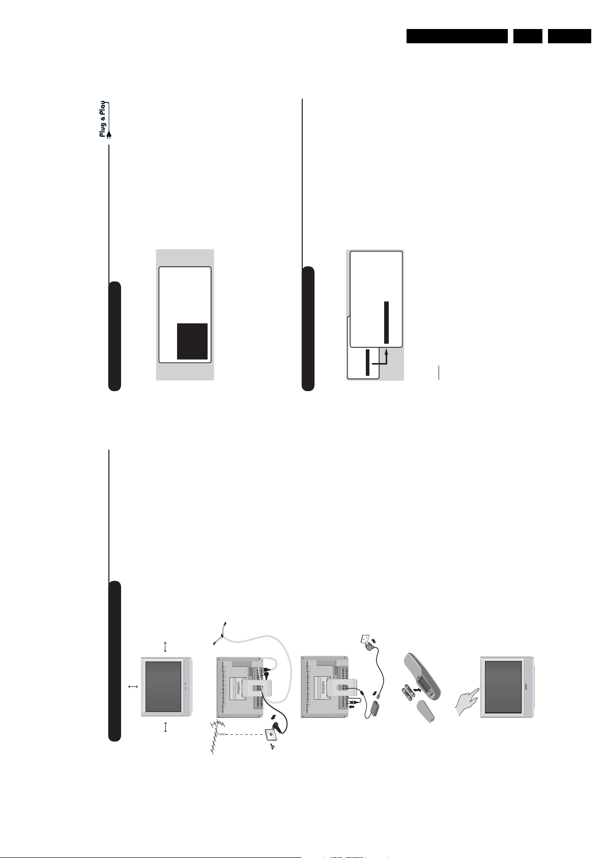
Technical Specifications, Connections, and Chassis Overview
1. Technical Specifications, Connections, and Chassis Overview
1.1 Technical Specifications
1.1.1 Reception
Tuning system : PLL
Colour systems : PAL B/G,
: PAL D/K,
: SECAM B/G,
: SECAM D/K
: SECAM L,
: SECAM L1
:
Sound system : 2CS BG,
: NICAM B/G,
: NICAM D/K,
: NICAM I,
: NICAM L,
Built-in radio type : FM
Speakers : Full range
: 13”: 2 x 3 W_rms
: 15”: 2 x 3 W_rms
: 20”: 2 x 5 W_rms
Frequency bands : UVSH
IF Freq. : 38.9 MHz
Channel selections : 100 channels
: Full cable, UVSH
Aerial input : 75 ohm
: Coax IEC-type
Pixel format : 13”: 640 x 480 (VGA)
: 15”: 1024 x 768 (XGA)
: 20”: 640 x 480 (VGA)
Viewing angle : 13”: 120 x 90 degrees
: 15”: 176 x 170
degrees
: 17”: 176 x 170
degrees
1.1.2 Miscellaneous
Mains voltage 13”/15” : External power
Supply
: Input: 100-240 Vac,
: 1.5 A
: Output: 12V dc,
: +/- 0.6 V, 60 W
Mains voltage 20” : External power
Supply
: Input: 100-240 V ac,
: 1.5 A
: Output: 24V dc,
: +/- 1.2 V, 120 W
Mains frequency : 50/60 Hz
Operating temperature : + 5 to + 35 deg. C
Storage temp. : -20 to 60 deg. C.
Maximum humidity : 90% R.H. max
(< 40(ºC)
Power dissipation : 13”: 35 W
: 15”: 50 W
: 20”: 60 W
Standby Power dissipation : 1 W
Weight : 13”: 4.5 kg
: 15”: 5.0 kg
: 20”: 8.5 kg
Dim. 13” model (WxHxD) : 344x322x65 mm
Dim. 15” model (WxHxD) : 377x361x70 mm
Dim. 20” model (WxHxD) : 477x435x81 mm
1.2 Controls
1.2.1 Front + Top Controls
TOP CONTROLS
+
-
FRONT CONTROLS
LED IR
CL 36532073_040.eps
<
<
011203
Figure 1-1 Front + Top Controls.
1.3 Connections
1.3.1 Left side Connections A/V
LEFT SIDE CONNECTIONS
HEADPHONE
S
Video
Video
in
L
Audio
in
R
CL 36532073_108.eps
Figure 1-2 Left side connections.
Audio - Out
- Headphone,
stereo 32 - 600 ohm/10 mW o
S-VHS - In (Hosiden)
1 - Y Ground H
2 - C Ground H
3 - Y 1 Vpp/75 ohm j
4 - C 0.3 Vpp/75 ohm j
Video - In (Cinch)
- CVBS 1 Vpp/75 ohm jq
Audio - In (Cinch)
- Audio - L 0.5 Vrms/10 kohm jq
- Audio - R 0.5 Vrms/10 kohm jq
1.3.2 Bottom Connections
BOTTOM CONNECTIONS
DC in
CL 36532073_044.eps
Figure 1-3 Bottom Connections
060104
FM ANT
291003

Technical Specifications, Connections, and Chassis Overview
DC - In
- 13”/15”: 12 V_dc/5A/60 W
20”: 24V_dc/5A/60 W jr
Aerial - In (IEC)
- IEC type 75 ohm, coax D
FM Ant (IEC)
- IEC type 75 ohm, coax D
1.3.3 Rear Connections
SCART EXT1 - In/Out (RGB/YUV and CVBS)
121
EN 3LC13E 1.
CL96532137_056.eps
Figure 1-4 Rear connections
1 - Audio - R 0.5 Vrms/1 kohm k
2 - Audio - R 0.5 Vrms/10 kohm j
3 - Audio - L 0.5 Vrms/1 kohm k
4 - Audio Ground H
5 - Blue Ground H
6 - Audio - L 0.5 Vrms/10 kohm j
7 - Blue 0.7 Vpp/75 ohm j
8 - CVBS-status 0 - 1.3 V: INT
4.5 - 7 V: EXT 16:9
9.5 - 12 V: EXT 4:3 j
9 - Green Ground H
10 - N.C.
11 - Green 0.7 Vpp/75 ohm j
12 - N.C.
13 - Red Ground H
14 - Blanking Ground H
15 - Red 0.7 Vpp/75 ohm j
16 - RGB-status/
FBL 0 - 0.4 V: INT
1 - 3 V: EXT/75 ohm j
17 - Video in/out Ground H
18 - RGB sw. ctrl Ground H
19 - CVBS-out 1 Vpp/75 ohm k
20 - CVBS-in 1 Vpp/75 ohm j
21 - Common Ground H
202
171199
EN 4 LC13E1.
1.4 Chassis Overview
1.4.1 13”/15” model
TOP CONTROL PANEL
E
Technical Specifications, Connections, and Chassis Overview
LCD PANEL
TO LCD PANEL
INVERTER
IN
PANEL
SCALER
C
BOARD
FRONT LED
J
1.4.2 20” model
PANEL
Right
Speaker
1402_8P
ComPair
Figure 1-5 Chassis Overview 13”/15” model
Left
Speaker
TV
BOARD
CL 36532073_054.eps
A
191103
TOP CONTROL PANEL
E
INVERTER
IN
PANEL
SCALER
C
BOARD
FRONT LED
J
PANEL
Right
Speaker
LCD PANEL
TO LCD PANEL
ComPair
Left
Speaker
TV BOARD
CL 36532073_055.eps
A
191103
Figure 1-6 Chassis Overview 20” model

Safety Instructions, Warnings, and Notes
2. Safety Instructions, Warnings, and Notes
EN 5LC13E 2.
2.1 Safety Instructions
Safety regulations require that during a repair:
• Always connect the set to the mains via an isolation
transformer (≥ 800 VA).
• Replace safety components, indicated by the symbol h,
only by components identical to the original ones.
Safety regulations require that after a repair, the set must be
returned in its original condition. Pay, in particular, attention to
the following points:
• Route the wire trees and HT cables correctly and fix them
with the mounted cable clamps.
• Check the insulation of the mains lead for external
damage.
• Check the cabinet for defects, to avoid touching of any
inner parts by the customer.
2.2 Warnings
• All ICs and many other semiconductors are susceptible to
electrostatic discharges (ESD w). Careless handling
during repair can reduce life drastically. Make sure that,
during repair, you are connected with the same potential as
the mass of the set by a wristband with resistance. Keep
components and tools also at this same potential.
Available ESD protection equipment:
– Complete kit ESD3 (small tablemat, wristband,
connection box, extension cable and earth cable) 4822
310 10671.
– Wristband tester 4822 344 13999.
• Be careful during measurements in the high voltage
section (on the inverter panel).
• Never replace modules or other components while the unit
is switched 'on'.
• When you align the set, use plastic rather than metal tools.
This will prevent any short circuits and the danger of a
circuit becoming unstable.
2.3 Notes
2.3.1 General
• Clean the LCD display with a slightly humid cloth.
• Measure the direct voltages and oscillograms with regard
to the chassis ground (H), or hot ground (I) as this is
called.
• The direct voltages and oscillograms shown in the
diagrams are indicative. Measure them in the Service
Default Mode (see section “Service Modes”).
• Where necessary, measure the voltages in the power
supply section both in normal operation (G) and in standby
(F). These values are indicated by means of the
appropriate symbols.
• The semiconductors indicated in the circuit diagram and in
the parts lists, are interchangeable per position with the
semiconductors in the unit, irrespective of the type
indication on these semiconductors.
• Capacitor values may also use the value multiplier as the
decimal point indication (e.g. 2p2 indicates 2.2 pF).
• An 'asterisk' (*) indicates component usage varies. Refer to
the diversity tables for the correct values.
• The correct component values are listed in the Electrical
Replacement Parts List. Therefore, always check this list
when there is any doubt.
2.3.3 Rework on BGA ICs
General
Although (LF)BGA assembly yields are very high, there may
still be a requirement for component rework. By rework, we
mean the process of removing the component from the PWB
and replacing it with a new component. If an (LF)BGA is
removed from a PWB, the solder balls of the component are
deformed drastically so the removed (LF) BGA has to be
discarded.
Device Removal
As is the case with any component, it is essential when
removing an (LF) BGA that the board, tracks, solder lands, or
surrounding components are not damaged. To remove an
(LF)BGA, the board must be uniformly heated to a temperature
close to the reflow soldering temperature. A uniform
temperature reduces the chance of warping the PWB.
To do this, we recommend that the board is heated until it is
certain that all the joints are molten. Then carefully pull the
component off the board with a vacuum nozzle. For the
appropriate temperature profiles, see the IC data sheet.
Area Preparation
When the component has been removed, the vacant IC area
must be cleaned before replacing the (LF)BGA.
Removing an IC often leaves varying amounts of solder on the
mounting lands. This excessive solder can be removed with
either a solder sucker or solder wick. The remaining flux can be
removed with a brush and cleaning agent.
After the board is properly cleaned and inspected, apply flux on
the solder lands and on the connection balls of the (LF) BGA.
Note: Do not apply solder paste, as this has shown to result in
problems during re-soldering.
Device Replacement
The last step in the repair process is to solder the new
component on the board. Ideally, the (LF)BGA should be
aligned under a microscope or magnifying glass. If this is not
possible, try to align the (LF)BGA with any board markers.
To reflow the solder, apply a temperature profile according to
the IC data sheet. So as not to damage neighbouring
components, it may be necessary to reduce some
temperatures and times
2.3.2 Schematic Notes
• All resistor values are in ohms and the value multiplier is
often used to indicate the decimal point location (e.g. 2K2
indicates 2.2 kohm).
• Resistor values with no multiplier may be indicated with
either an 'E' or an 'R' (e.g. 220E or 220R indicates 220
ohm).
• All Capacitor values are expressed in Micro-Farads (µ=
-6
x10
), Nano-Farads (n= x10-9), or Pico-Farads (p= x10
-12
).
EN 6 LC13E3.
3
12
MENU
”
P
564
879
0
3
--
++
.
[
Ÿ
Á
-
ª
`
ù
SMART
SMART RADIO
Ë
¤
ı
Y
Ó
Remote control keys
ı
List of programmes
To display/ clear the list of programmes.
Use the keys
îÏ
to select a
programme and the key
¬
to display it.
The symbol
+
is displayed alongside
all programmes which are locked (p.9) or
?
if they are not locked.
Screen information
To display / remove the programme
number,the name (if it exists), the
time, the sound mode and the time
remaining on the timer. Hold down
for 5 seconds to permanently
display the programme number on
the screen.The volume level and the
smart control adjustments are then
displayed each time they are used.
Menu
To call up or exit the menus.
Sleeptimer
To select the length of time before
the set automatically switches to
standby (from 0 to 240 minutes).
Cursor / Format 16:9
These 4 keys are used to navigate
through the menus.The
Ȭ
keys are used to enlarge or
compress the picture vertically.
Volume
To adjust the sound level.
Mute
To mute or restore the sound.
Select peripherals (p.11)
Press several times to select the
required EXT connector.
Numerical keys
For direct access to programmes.
For a 2 digit programme number,
the 2
nd
digit must be entered
before the dash disappears.
Standby
To set the TV to standby mode.
To switch the TV set on again,
press
b
,P
@#
or
09
.
Radio / TV mode
To switch the TV set to radio or
TV mode .
Teletext (p. 10)
Teletext keys (p.10)
Smart picture and sound
Used to access a series of
predefined
picture and sound
settings.
The PERSONAL position relates to
settings selected from the menus.
Selecting TV programmes
To move up or down a programme.
The number,(the name) and the
sound
mode are displayed for a few
seconds.
For some TV programmes the title of
the programme appears at the
bottom of the screen.
Previous programme
To access the previously viewed
programme.
Sound mode
Used to force programmes in STEREO
and
NICAM STEREO
to
MONO
or,
for bilingual programmes, to choose
between
DUAL I
or
DUAL II
.
When the sound mode is switched to
MONO, the indication is displayed in red.
2
Presentation of the LCD Television
Television keys:
• .: to switch the TV on or off.
• - + : to adjust sound level.
• <> : to select programmes.
• MENU: to access or close menus, simultaneously
press the - and + keys. The <> keys can be used to
select an adjustment and the - + keys to make that
adjustment.
Note
: when the CHILD LOCK function is activated the
- + and <> keys are unavailable (refer to FEATURES
menu on page 9).
On-light and infrared sensors.
Rear of set :
The main connections are made at the bottom of the television.
For more details on connections see page 12.
EXT1 socket
Side connections
Adjustable stand.
The stand can be removed and replaced with a
wall mounting kit available as an option (ask your
dealer).
TV and radio aerial sockets
DC supply socket
3. Directions for Use
Directions for Use
<
<
.
+
-
S
*
Video
L
R
in
in
Video
Audio
EXT1
FM ANT
:
DC in
Directions for Use
5
Quick installation
Sorting programmes
The first time you switch on the television, a
menu appears on the screen.This menu asks
you to choose the language of the menus :
If the menu does not appear, hold down the - and +
keys on the set for 8 seconds to bring it up.
& Use the
îÏ
keys on the remote control to
choose your language then confirm with
¬
.
é Then select your country using the
îÏ
keys and confirm with
¬
.
If your country does not appear in the list, select “.. .”
“ Tuning starts automatically.
The operation takes several minutes.
A display shows the search status and the
number of programmes found.When it has
finished the menu disappears.
To exit or interrupt the search, press the
H
key.
If no programmes are found, refer to the chapter
entitled Tips on p. 12.
‘ If the transmitter or the cable network
broadcasts the automatic sort signal, the
programmes will be correctly numbered.
( If not, the programmes found will be numbered
in descending order starting at 99, 98,97, etc.
Use the SORT menu to renumber them.
Some transmitters or cable networks broadcast
their own sort parameters (region, language, etc.).
Where this is the case, make your choice using the
îÏ
keys and confirm with
¬
.
& Press the
H
key.The main menu is displayed.
é Select INSTALL (
Ï
), then press
¬
.
The INSTALL menu appears.
“ Using the
Ï
key, select SORT then press
¬
.The SORT menu appears.The FROM
option is activated.
Note:
this menu works as follows:
• Change "FROM" (enter the current programme
number),
• "TO" (enter the new number),
• EXCHANGE numbers" (the operation is carried out).
‘ Select the programme you wish to renumber
using
Ȭ
keys or
0
to
9
.
Example: to renumber programme 78 as
2 press
78
.
( Select TO (using
Ï
key) and enter the new
number with
Ȭ
keys or
0
to
9
(for the example given, enter
2
).
§ Select EXCHANGE (
Ï
key) and press
¬
.
The message EXCHANGED appears, the
exchange takes place. In our example,
programme 78 is renumbered as 2
(and programme 2 as 78).
è Select the option FROM (
î
key) and repeat
stages ‘ to § as many times as there are
programmes to renumber.
! To exit from the menus, press
d
.
• PICTURE
• SOUND
• FEATURES
• INSTALL
INSTALL
• LANGUAGE
• COUNTRY
• AUTO STORE
• MANUAL STORE
• SORT
• NAME
FROMTOEXCHANGE
SELECT LANGUAGE
LANGUAGE
•
ENGLISH
DANSK
NEDERLANDS
FINNISH
FRANCAIS
COUNTRY
AUSTRIA
BELGIUM
SWITZERLAND
GERMANY
DENMARK
4
& Positioning the television set
Place your TV on a solid stable surface. To avoid
danger do not expose the TV to water, or a heat
source (e.g. lamp, candle, radiator). Do not obstruct
the ventilation grid at the rear.
é
Connecting the aerials
• Connect the
:
socket situated at the bottom
of the TV to your aerial socket.
• Insert the radio aerial lead supplied into the FM
ANT socket located at the bottom of the TV.
• Arrange the leads by passing them through the
television stand.
“
Power supply connections
The TV works with a DC supply (the voltage is
indicated on the label). Only use the AC-DC
adaptor supplied with the TV.
• Connect the DC plug of the adaptor to the TV DC
socket. Leave a space round the adaptor for
ventilation.
• Insert the adaptor power lead and insert the mains
plug into the wall socket.
For connecting other appliances see page p.12.
‘
Remote control
Insert the two R6-type batteries supplied, making
sure they are the right way round.
The batteries supplied with the appliance do not
contain mercury or nickel cadmium so as to protect
the environment. Please do not discard your used
batteries, but use the recycling methods available
(consult your distributor).
(
Switching on
To switch on the set, press the on/off key.
A green indicator comes on and the screen lights
up. Go straight to the Quick Installation chapter on
page 5. If the TV remains in standby mode (red
indicator), press the P
#
key on the remote
control.
The indicator will flash when you use the remote control.
Installing your television set
EN 7LC13E 3.
5 cm
5 cm
5 cm
FM ANT.
EN 8 LC13E3.
7
Manual tuning
This menu allows you to store the
programmes one by one.
& Press
H
.
é Select INSTALL (
Ï
), then press
¬
.
The INSTALL menu appears.
“ Select MANUAL STORE (
Ï
) then press
¬
.
The menu appears :
‘ Press
¬
to go to the SYSTEM menu.
Use
îÏ
to choose EUROPE (automatic
detection*) or manual detection with WEST
EUR (standard BG reception), EAST EUR
(standard DK reception), UK (standard I
reception) or FRANCE (standard LL').
Then press
È
to exit from the menu.
* Except for France (standard LL'): select the
option FRANCE.
( Select SEARCH and press
¬
.
The search begins.As soon as a programme is
found, the search will stop. If you know the
frequency of the programme required,enter
its number directly using the
09
keys and
go to step è.
If no programme is found, refer to the Tips chapter
on page 12).
§ If reception is un-satisfactory,select FINE
TUNE and hold down
È
or
¬
key.
è Select PROG.NO (programme number) and
use the
Ȭ
or
0
to
9
keys to enter
the desired number.
! Select STORE and press
¬
.The message
STORED appears.The programme is stored.
ç Repeat steps ( to ! for each programme to
be stored.
To exit: press the
d
key.
• PICTURE
• SOUND
• FEATURES
• INSTALL
INSTALL
MANUAL STORE
• SYSTEM
• SEARCH
• PROG. NO.
• FINE TUNE
• STORE
EUROPE
WEST EUR
EAST EURUKFRANCE
Using the radio
Choosing radio mode
Press the
Â
key on the remote control to
switch the TV to radio mode.
In radio mode the number and name of the
station (if available), its frequency and the
sound mode are indicated on the screen.
To enter the name of the stations use the NAME
menu. (p.7)
Selecting programmes
Use the
09
or
@
P
#
keys to select the
FM stations (from 1 to 40).
List of radio stations
Press the
ı
key to display / hide the list of
radio stations.Then use the cursor to select a
station.
Using the radio menus
Use the
H
key to access the specific radio
settings.
Searching radio stations
If you have used the quick installation all the
available FM stations will be stored.To start a
new search use the INSTALL menu :
AUTO STORE (for a complete search) or
MANUAL STORE (for a station by station
search).
The SORT and NAME menus let you classify
or name the radio stations.These menus work
in exactly the same way as the TV menus.
Screen saver
In the FEATURES menu you can activate /
close the screen saver.The time, the frequency
of the station and its name (if available) move
across the screen.
6
Programme name
You may,if you wish, give a name to the first
40 programmes (from 1 to 40).
& Press
H
.
é Select INSTALL (
Ï
), then press
¬
.
The INSTALL menu appears.
“ Press
Ï
5 times to select NAME (concealed
at the bottom of the screen), then press
¬
.
The menu appears :
‘ Select the programme you wish to name using
the keys
09
or
@
P
#
.
Note:
at the time of installation, the programmes
are automatically named when the identification
signal is transmitted.
( Use the keys
Ȭ
to move within the
name display area (5 characters).
§ Use keys
îÏ
to choose the characters.
è Press
H
when the name has been entered.
The programme name is stored.
! Repeat steps ‘ to è for each programme to
be named.
ç To exit from the menus, press
d
.
INSTALL
• LANGUAGE
• COUNTRY
• AUTO STORE
• MANUAL STORE
• SORT
•
NAME
BBC_1
Choosing a language and country
Automatic tuning
& Press the
H
key to display the main menu.
é Select INSTALL (
Ï
), then press
¬
.
The INSTALL menu appears.
The LANGUAGE option is activated.
“ Press
¬
to go into the LANGUAGE menu.
‘ Select your language with the
îÏ
keys.
The menus will appear in the chosen language.
( Press
È
to exit the LANGUAGE menu.
§ Select the option COUNTRY and press
¬
.
è Select your country with
îÏ
keys.
If your country does not appear in the list, select
OTHER.
! Press
È
to exit the COUNTRY menu.
ç To exit from the menus, press
d
.
This menu allows you to automatically search
for all the programmes available in your region
(or on your cable network).
& First carry out operations & to ! above,then:
é Press
Ï
once to select AUTO STORE then
press
¬
.The search begins.
After several minutes, the INSTALL menu
reappears automatically.
“ If the transmitter or the cable network
broadcasts the automatic sort signal, the
programmes will be correctly numbered.
‘ If not, the programmes found will be
numbered in descending order starting at 99,
98, 97,etc.
Use the SORT menu to renumber them.
Some transmitters or cable networks broadcast
their own sort parameters (region, language, etc.).
Where this is the case, make your choice using the
îÏ
keys and confirm with
¬
.
To exit or interrupt the search, press the
H
key.
If no picture is found, refer to the chapter entitled
Tips on p. 12.
( To exit from the menus, press
d
.
• PICTURE
• SOUND
• FEATURES
• INSTALL
INSTALL
• LANGUAGE
• COUNTRY
• AUTO STORE
• MANUAL STORE
• SORT
•
NAME
ENGLISH
DANSK
NEDERLANDS
INSTALL
• LANGUAGE
• COUNTRY
• AUTO STORE
• MANUAL STORE
• SORT
•
NAME
SEARCHING
PLEASE WAIT
PROG. NO. 2
215.18 MHZ
Directions for Use
Directions for Use
9
Timer function
Locking the set
This menu allows you to use your TV as an
alarm clock.
& Press
H
.
é Select
FEATURES
(
Ï
) and press
¬
twice.
The
TIMER
menu appears :
“ Press
¬
to enter and exit the sub-menus
and use keys
îÏ
to adjust:
‘
TIME
: enter current time.
Note:
the time is updated automatically each time
the set is switched on using teletext information
taken from programme 1. If programme 1 does
not have teletext, the update will not take place.
(
START TIME
: enter the start time.
§
STOP TIME
: enter the stop time.
è
PROG.NO.
: enter the number of the
programme for the wake-up alarm.For models
equipped with a radio, you can select an FM
station by using the
Ȭ
keys (the
09
keys are only used to select TV programs).
!
ACTIVATE
: you can set the alarm to be
activated:
•
ONCE ONLY
for a one-off alarm,
•
DAILY
for a daily alarm or
• OFF to cancel.
ç Press
b
to set the TV to standby. It will
automatically switch on at the time
programmed. If you leave the TV switched on,
it will only change programme at the time
indicated.
The combination of the CHILD LOCK and TIMER
functions may be used to limit the length of time
your television is in use, for example, by your
children.
You can bar access to certain programmes or
completely lock the set by locking the keys.
Locking programmes
& Press
H
.
é Select (
Ï
) and press
¬
.
“ Select
PARENTAL. CONT.
(
Ï
) and press
¬
.
‘ Enter your confidential access code.The first
time, enter the code 0711 then confirm by
re-entering 0711.The menu appears.
( Press
¬
to go into the menu.
§ Use keys
îÏ
to select the required
programme and confirm with
¬
.The symbol
+
is displayed alongside the programmes or
sockets that have been locked.
è Press
d
to exit.
To watch a programme which has been locked
you will now need to enter the confidential
code; otherwise the screen will remain blank.
The INSTALL menu access is also locked.
Caution:
in the case of encrypted programmes
which use an external decoder, it is necessar y to
lock the corresponding EXT socket.
To unlock all programmes
Repeat stages & to ‘ above, then select
CLEAR ALL
and press
¬
.
To change the confidential code
Repeat stages & to ‘ above, then:
( Select
CHANGE CODE
and enter your own
4-digit number.
§ Confirm by entering it again.
Your new code will be stored.
è Press
d
to exit from the menus.
If you have forgotten your confidential code, enter
the universal code 0711 twice.
Locking the keys
& Press
H
, select
FEATURES
(
Ï
) and press
¬
.
é Select
CHILD LOCK
(
Ï
) and press
¬
to set
the lock to
ON
.
“ Switch off the set and put the remote control
out of sight.The set cannot be used (it can only
be switched on using the remote control).
‘ To cancel: switch
CHILD LOCK
to
OFF
.
• PICTURE
• SOUND
• FEATURES
• INSTALL
FEATURES
TIMER
• TIME
• START TIME
• STOP TIME
• PROG; NO;
• ACTIVATE
10:56
• PICTURE
• SOUND
• FEATURES
• INSTALL
FEATURES
• TIMER
• MODE SELECT
• CHILD LOCK
• PARENTAL CONT
ACCES CODE
- - - -
8
Adjusting the picture
Adjusting the sound
& Press
H
then
¬
.
The
PICTURE
menu appears :
é Use
îÏ
keys to select a setting and
Ȭ
keys to adjust.
Note:
the menu is a scroll-down menu.
Keep the key
Ï
held down to access the
settings hidden at the bottom of the screen.
“ Once the necessary adjustments have been
made, select the option
STORE
and press
¬
to store them.
‘ To exit from the menus, press
d
.
Description of the settings:
•
BRIGHTNESS
: alters the brightness of the
image.
•
COLOUR
: alters the colour intensity.
•
CONTRAST
: alters the variation between
light and dark tones.
•
SHARPNESS: alters the crispness of the image.•STORE
: stores the picture settings.
• NR: attenuates picture noise (snow) in
difficult reception conditions.
•
CONTRAST +
:To activate / de-activate the
automatic contrast adjustment system
(the dark areas are made darker whilst
maintaining the detail).
& Press
H
, select the
SOUND
option (
Ï
) and
press
¬
.The
SOUND
menu appears :
é Use
îÏ
keys to select a setting and keys
Ȭ
to adjust.
“ Once the necessary adjustments have been
made, select the option
STORE
and press
¬
to store them.
‘ To exit from the menus, press
d
.
Description of the settings:
•
EQUALIZER
: to adjust the sound tone (from
bass: 120 Hz to treble: 10 kHz).
•
BALANCE
: to balance the sound between the
left and right speakers.
•
DELTA VOLUME
(volume difference):allows you
to compensate for the volume differences
between the different programmes or the
EXT sockets.This setting is available for
programmes 1 - 40 and the EXT sockets.
Use the
@
P
#
keys to compare the level
of different programmes.
•
STORE
: stores the sound settings.
•
AVL
: automatic volume control used to avoid
sudden increases in volume, particularly when
changing programmes or during advertisements.
•
INCR. SURROUND
:To activate / deactivate the
surround sound effect. In stereo, this gives the
impression that the speakers are further apart.
In mono, a stereo spatial effect is simulated.
• PICTURE
• SOUND
• FEATURES
• INSTALL
PICTURE
• BRIGHTNESS
• COLOUR
• CONTRAST
• SHARPNESS
• STORE
• NR
• CONTRAST+
--I------ 39
• PICTURE
• SOUND
• FEATURES
• INSTALL
SOUND
• EQUALIZER
•
BALANCE
• DELTA VOLUME
• STORE
• AVL
• INCR. SURROUND
120 HZ
500 HZ
1500 HZ
5 KHZ
10 KHZ
Feature settings
& Press
H
, select
FEATURES
(
Ï
) and press
¬
.You can adjust:
é
TIMER
,
PARENTAL. CONT.
and
CHILD LOCK
:
see next page
“
MODE SELECT.
: to switch the TV in radio or
TV.
‘ To quit the menus, press
d
.
EN 9LC13E 3.
EN 10 LC13E3.
11
MODE
VCR
DVD
·¢Ê Æ
∫
Ó
ı
Ω∆
.
Z
¤
Make the connections as shown opposite.With the
n
key,
select
EXT3
.
For a monophonic device, connect the audio signal to the AUDIO L
input.The sound automatically comes out of the left and right
speakers of the set.
Headphones
When headphones are connected, the sound on the TV set will
be cut.The
@
P
#
keys are used to adjust the volume level.
The headphone impedance must be between 32 and 600 Ohms.
Side connections
L
R
Audio
in
*
Video
in
S
Video
Connecting peripheral equipment
The EXT1 socket has audio, CVBS/RGB inputs and audio, CVBS outputs.
Video recorder (or DVD recorder)
Carry out the connections shown opposite, using a good
quality euroconnector cable.
If your video recorder does not have a euroconnector socket, the
only connection possible is via the aerial cable.You will therefore
need to tune in your video recorder's test signal and assign it
programme number 0 (refer to manual store, p. 7).
To reproduce the video recorder picture,press
0
.
Video recorder with decoder
Connect the decoder to the second euroconnector socket of
the video recorder.You will then be able to record scrambled
transmissions.
Video recorder
Satellite receiver, decoder, DVD,games, etc.
Make the connections as shown opposite.
To select connected equipment
Press the
n
key to select
EXT1
and
EXT3
.
Most equipment (decoder, video recorder) carries out the switching
itself.
Other equipment
FM ANT
:
EXT1
VCR
EXT1
10
Teletext
Press :
You will obtain:
Teletext is an information system broadcast by certain channels which can be consulted like a
newspaper. It also offers access to subtitles for viewers with hearing problems or who are not familiar
with the transmission language (cable networks, satellite channels, etc.).
Teletext
on/off
Selecting
a page
This is used to call teletext, change to transparent mode and
then exit.The summary appears with a list of items that can be
accessed. Each item has a corresponding 3 digit page number.
If the channel selected does not broadcast teletext, the indication
100 will be displayed and the screen will remain blank (in this
case, exit teletext and select another channel).
Enter the number of the page required using the
0
to
9
or
@ P #
keys. Example: page 120,enter
120
.The
number is displayed top left,the counter turns and then the
page is displayed.Repeat this operation to view another page .
If the counter continues to search, this means that the page is not
transmitted. Select another number.
Contents
Direct
access to
the items
This returns you to the contents page (usually page 100).
Coloured areas are displayed at the bottom of the screen.
The 4 coloured keys are used to access the items or
corresponding pages.
The coloured areas flash when the item or the page is not yet
available.
Enlarge
a page
This allows you to display the top or bottom part of the
page and then return to normal size.
Stop sub-page
acquisition
Hidden
information
Certain pages contain sub-pages which are automatically
displayed successively.This key is used to stop or resume
sub-page acquisition.The indication
_
appears top left.
To display or hide the concealed information (games
solutions).
Favourite
pages
Instead of the standard coloured areas displayed at the
bottom of the screen, you can store 4 favourite pages on the
first 40 channels which can then be accessed using the
coloured keys (red, green,yellow, blue).Once set, these
favourite pages will become the default every time tetetext is
selected.
&
Press the
H
key to change to favourite pages mode.
é
Display the teletext page that you want to store.“Press
d
then the coloured key of your choice.
The page is stored.
‘
Repeat steps
é
and
“
for the other coloured keys.
(
Now when you consult teletext, your favourite pages
will appear in colour at the bottom of the screen.
To temporaly retrieve the standard items, press
H
.
To clear everything, and return the standard items as the
default, press
d
for 5 seconds.
Directions for Use
¤
.
9
0
ŸÓù
¤
ª-
SMART RADIO SMART
Ë
MENU
P
P
+
-
[
-
123
+
”
56
4
Ë
Á
0
Ø
789
Ó
Ÿ
MENU
Ë
4. Mechanical Instructions
Index of this chapter:
1. Service Position
2. Rear Cover Removal
3. I/O Cover Removal
4. LED/Remote Control Board Removal
5. TV Board Removal
6. Scaler Board Removal
7. Inverter Board Removal
8. Top Control Assy Removal
9. LCD Panel Removal
10. Re-assembly
Note: Figures below can deviate from the actual situation, due
to different set executions and screen sizes.
4.1 Service Position
First, put the TV in its service position. Therefore, place it
upside down on a tabletop, use a protection sheet or a foam
cushion. Take care that this is flat and free from obstacles like
screws, to prevent damaging the fragile LCD screen. ESD
protective service buffers, as shown below, can be used
(3122 785 90580).
Mechanical Instructions
EN 11LC13E 4.
CL 36532073_058.eps
011203
CL 36532073_057.eps
Figure 4-1 Service position with ESD protective service buffers
261103
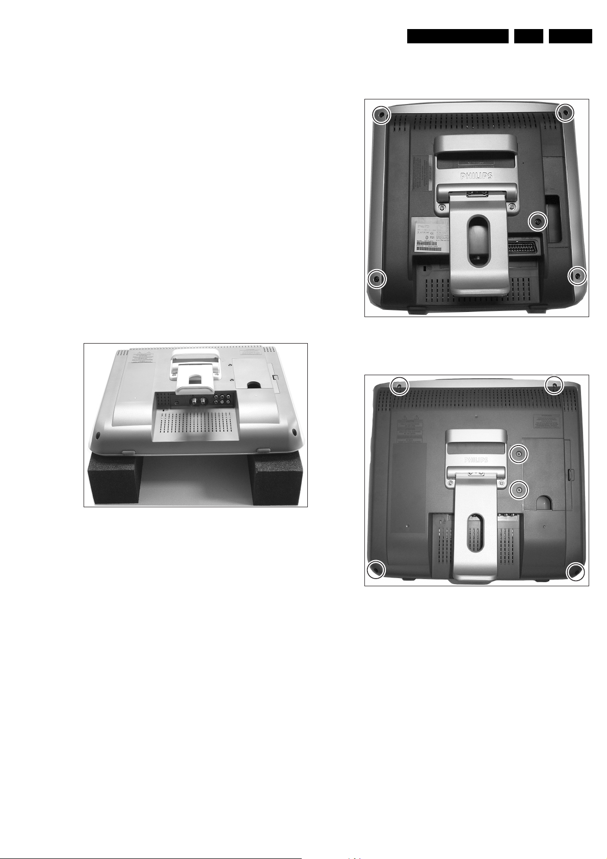
4.2 Rear Cover Removal
1. Use a Torx (T10) screwdriver to remove the rear cover by
unscrewing and removing the screws as indicated by the
figures: Rear cover removal 13-inch and 20-inch.
2. Make sure all power-, audio-, video-, coax-, cinch- and
SCART cables are unplugged.
3. The number of Torx screws to be removed are: six for the
13- and 15-inch version and seven for the 20-inch.
4. Carefully remove the rear cover and store it on a safe
place.
Figure 4-2 Rear cover removal 13- and 15-inch
CL 36532073_059.eps
Figure 4-3 Rear cover removal 20-inch
271103
EN 12 LC13E4.
Mechanical Instructions
CL 36532073_060.eps
Figure 4-4 Rear cover removal hidden screw EU version
CL 36532073_061.eps
Figure 4-5 Rear cover removal hidden screws US version
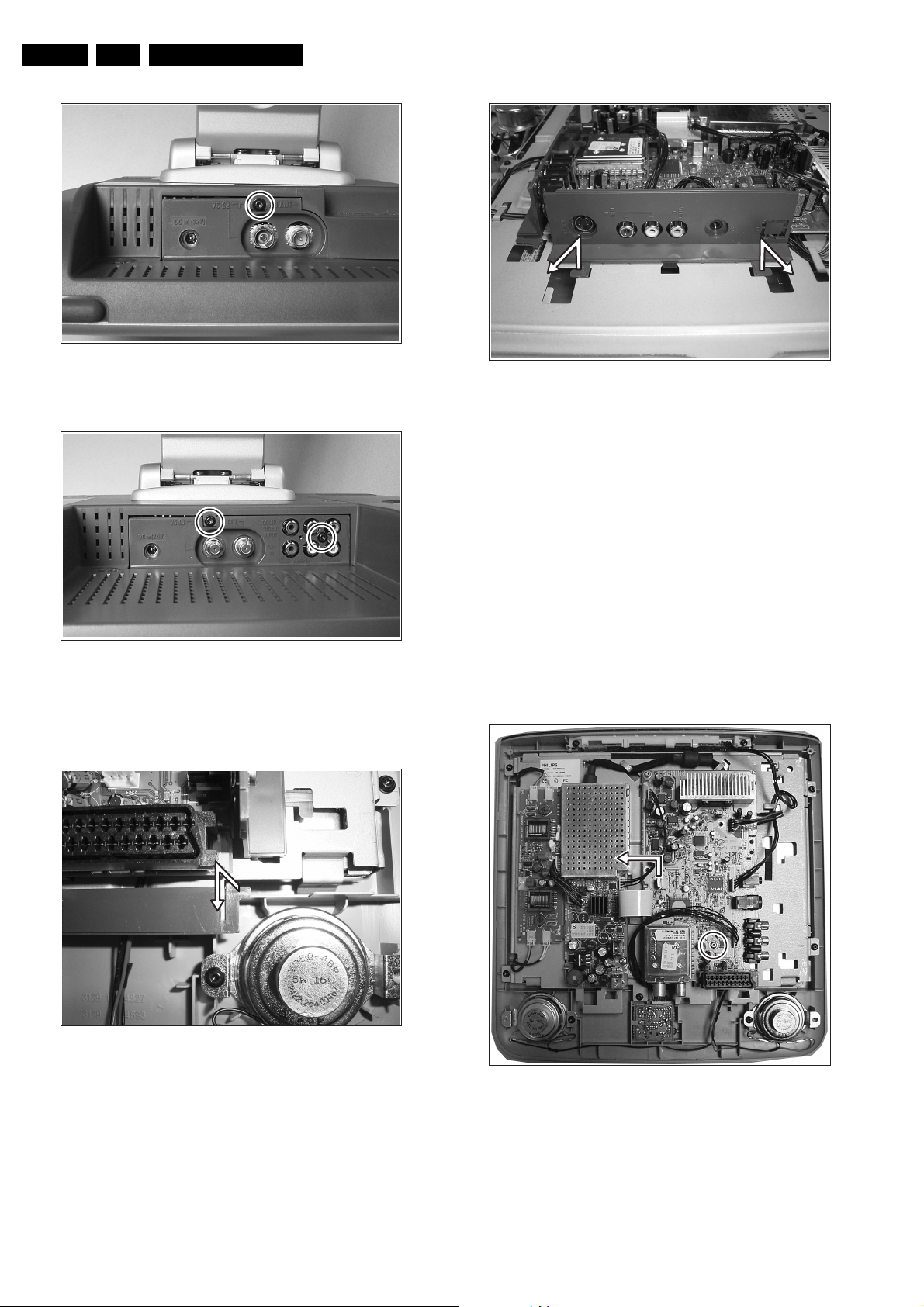
4.3 I/O Cover Removal
261103
261103
CL 36532073_063.eps
Figure 4-7 IO cover side
1. Lift up both tags (securing clips) and at the same time pull
it away from the TV board.
4.4 LED/Remote Control Board Removal
1. Unlock the securing clip, which holds the PWB in place,
and take out the LED/Remote control PWB.
4.5 TV Board Removal
1. Disconnect all four PWB connectors out of the regarding
sockets 1231, 1234, 1732 and 1902.
2. Pull the thin flat cable out of its special shaped connector,
1010.
3. Unscrew and remove the two PWB mounting screws.
4. Take out the TV board in the indicated direction.
271103
CL 36532073_062.eps
261103
Figure 4-6 IO cover bottom
1. Lift up the tag (securing clip) at the right side of the IO cover
and at the same time pull it away from the TV board.
CL 36532073_064.eps
271103
Figure 4-8 TV board
Note: Sometimes it is necessary to place the Scaler board in a
service position. In this case, it is necessary to use the specific
“Repair kit scaler board” including two extra long cables (order
nr. 3122 785 90490).
Mechanical Instructions
EN 13LC13E 4.
LVDS CABLE
Figure 4-9 Service position TV board
4.6 Scaler Board Removal
4.6.1 13 and 20 inch versions
1. Carefully remove the shielding covering the top part of the
Scaler board.
2. Carefully disconnect the TTL cable connector in the centre
of the board (1501). Take care not to damage the fragile
cables.
3. Disconnect the cable connectors at the edge of the board
(1342 and 1003).
4. Pull the thin flat cable out of its special shaped connector
(1681).
5. Unscrew and remove both PWB mounting screws.
6. Take out the Scaler PWB.
TTL CABLE
CL 36532073_065.eps
271103
CL 36532073_067.eps
271103
Figure 4-11 Scaler PWB
Note: Sometimes it is necessary to place the Scaler board in a
service position. In this case, it is necessary to use the specific
“Repair kit scaler board” including two extra long cables (order
nr. 3122 785 90490).
CL 36532073_068.eps
271103
Figure 4-10 Scaler PWB
4.6.2 15 inch version
1. Carefully disconnect the LVSD cable connector at the top
of the board (1506). Take care not to damage the fragile
cables.
2. Disconnect the cable connectors at the edge of the board
(1342 and 1003).
3. Pull the thin flat cable out of its special shaped connector
(1681).
4. Unscrew and remove both PWB mounting screws.
5. Take out the Scaler PWB.
CL 36532073_066.eps
271103
Figure 4-12 Service position Scaler Board
Important: Video converter chip heat sink.
Figure 4-13 Heat sink removal
CL 36532073_069.eps
181203
EN 14 LC13E4.
Mechanical Instructions
1. Use a pair of pliers to take off the heat sink by means of a
twist- and pull movement (see figure), before you de-solder
the video converter chip SAA7118 from the board. Store
the heat sink on a safe place, adhesive side up!
2. Place the self-adhesive heat sink back in place after the
chip exchange action has been finished.
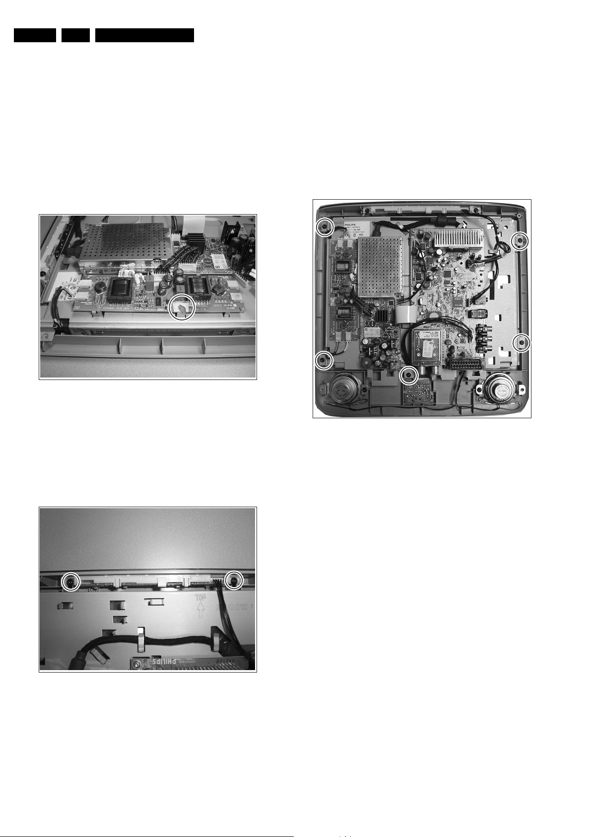
4.7 Inverter Panel Removal
1. Disconnect the 8-pole cable from the PWB.
2. Disconnect at top and bottom side all cable connectors.
3. Use a pair of pliers to bend the metal securing clamp in
such a way that the PWB can be taken out.
4. Remove the Inverter PWB and store it on a safe place.
4.9 LCD Panel Removal
In order to remove the LCD panel make sure that the TV board
is removed. See previous paragraph(s).
1. Carefully disconnect the LVDS or TTL cable connector,
which is revealed now, from LCD panel (CN1). Take care
not to damage the fragile cables.
2. Unscrew and remove all five screws of the panel frame,
which secure the frame to the monitor front.
3. Take care that the tape securing the speaker cable assy is
removed, or loosened.
4. Remove the LCD panel metal cover frame, the LCD panel
can be removed now.
Figure 4-14 Inverter PWB
4.8 Top Control Assy Removal
1. Remove the cable from the Top control assy (1500).
2. Remove both mounting screws that secure the unit to the
monitor frame.
3. Take out the Top control assy.
CL 36532073_070.eps
271103
Figure 4-16 LCD panel frame screws
4.10 Re-Assembly
To re-assemble the whole set, do all processes in reverse
order.
Notes:
• Take extra care when reconnecting the inverter PWB
backlight connectors (black/white/pink). Connect them
properly to avoid “high voltage sparking”.
CL 36532073_072.eps
271103
Figure 4-15 Top control assy
CL 36532073_071.eps
271103

Service Modes, Error Messages, and Repair Tips
5. Service Modes, Error Messages, and Repair Tips
EN 15LC13E 5.
Index of this chapter:
1. Test Points
2. Service Modes
3. Errors
4. The “Blinking LED” Procedure
5. ComPair
6. Trouble Shooting Tips
5.1 Test Points
This chassis is equipped with test points in the service printing.
In the schematics test points are identified with a rectangle box
around Fxxx or Ixxx. On the PCB, test points are specifically
mentioned in the service manual as “half moons” with a dot in
the centre.
Measurements are performed under the following conditions:
• Video: colour bar signal.
• Audio: 3kHz left, 1kHz right.
5.2 Service Modes
5.2.1 Limited DST Support
This chassis does still have some limited Dealer Service Tool
(DST) support. The set can be put in two service modes via the
DST (RC7150, this remote is not available anymore). These
are the Service Default Mode (SDM) and the Service Alignment
Mode (SAM).
Installation Features Dealer
For easy installation and diagnosis, the DTS can be used.
When there is no picture (to access the error code buffer via the
OSD), DST can enable the functionality of displaying the
contents of the entire error code buffer via the blinking LED
procedure.
The dealer can use the RC7150 for programming the TV-set
with presets. Ten different program tables can be programmed
into the DST via a GFL or MG TV-set (downloading from the
GFL or MG to the DST; see GFL or MG service manuals) or by
the DST-I. For explanation of the installation features of the
DST, the directions for use of the DST are recommended.
5.2.2 Service Default Mode (SDM)
Purpose of SDM:
• To provide a situation with predefined settings to get the
same measurements as in this manual.
• To start the “Blinking LED” procedure.
• To have the possibility to override the 5V protection
Activating SDM:
• By transmitting the "DEFAULT" command with the RC7150
Dealer Service Tool (this works both while the set is in
normal operation mode or in the SAM).
• Standard RC sequence 0-6-2-5-9-6 followed by pressing
the “MENU”-button (this works both while the set is in
normal operation mode or in the SAM).
• By shorting pins 5 and 6 of connector 1170 of LED/RC
panel. Then apply DC supply from the AC-DC adaptor (not
required to remove the metal shielding).
Note: By temporarily shorting pins 5 and 6 of connector 1170
and then applying DC supply from the AC-DC adaptor, the 5V
protection is disabled.
Caution: Overriding the 5V protection should only be used for
a short period of time. In case of S/W protections (error 4) the
set will shutdown after 15 sec.
For recognition, “SDM” is displayed at the upper right corner of
the screen.
SDM Menu
SDM
CL 36532073_083.eps
Figure 5-1 SDM Menu
Deactivating SDM:
• Press the “EXIT”-button on the DST, or
• Press 0-0 on the standard RC, or
• Switch the set to Standby (the error buffer is NOT cleared).
Note: When the mains power is switched off while the set is in
SDM, the set will switch to SDM immediately when the mains
is switched on again.
The SDM sets the following pre-defined conditions:
• PAL/SECAM sets: tuning at 475.25 MHz PAL.
• Volume level is set to 25% (of the maximum volume level).
Other picture and sound settings are set to 50%.
The following functions are switched off in SDM (and after
leaving SDM):
• Timer.
• Sleep timer.
The following functions are disabled during SDM (and enabled
after leaving SDM)
• Parental lock.
• Blue mute.
• Hospitality Mode.
• No-ident Timer (normally the set is automatically switched
off when no video signal (IDENT) was received for 15
minutes).
All other controls operate normally.
Special Functions SDM
Access to normal user menu
Pressing the “MENU” button on the remote control switches
between the SDM and the normal user menus (with the SDM
mode still active in the background).
Channel search
Pressing the “P+” button of the remote control will select the
next available channel in the preset list.
Type nr, Error buffer, etc
Pressing the “OSD” or “info+” button of the remote control
shows/hides the type nr, error buffer, SW ID, Hours and option
codes. OSD can be hidden to prevent interference with
waveform measurements.
021203

EN 16 LC13E5.
Service Modes, Error Messages, and Repair Tips
Access to SAM
By pressing 0-6-2-5-9-6 “info+” (or OSD) in sequence on the
standard RC will switch from SDM to SAM.
5.2.3 Service Alignment Mode (SAM)
Purpose of SAM:
• To do alignments.
• To change option settings.
• To display/clear the error code buffer values.
• To store data in NVM
Note: to store the data in SAM mode main menu.
Activating SAM:
• By transmitting the "ALIGN" command with the RC7150
Dealer Service Tool (this works both while the set is in
normal operation mode or in the SDM).
• Standard RC sequence 0-6-2-5-9-6 followed by pressing
the “info+”-button (this works both while the set is in normal
operation mode or in the SDM).
Deactivating SAM:
• Press the “EXIT”-button on the DST, or
• Press 0-0 on the standard RC, or
• Switch the set to Standby (the error buffer is NOT cleared).
Note: When the AC-DC adaptor power is switched off while the
set is in SAM, the set will go back to normal mode of operation
when the AC-DC adaptor is switched on again.
In SAM the following information is displayed on the screen:
SAM Menu
TYPE: 17PF9945/012 HRS:0029
SWID: LC03E21-1.11
ERR : 0 0 0 0 0 0 0
OPT : 79 254 14 56 128 000
CLEAR ERRORS
OPTIONS
TUNER
WHITE TONE
Figure 5-2 SAM Menu
• Operation hours timer (hexadecimal).
• Software identification of the main micro controller of TV-
board (LC03BBC-X.YY).
– LC13 is the chassis name for 4 x 3 format LCD-TV.
– BBC is 1 letter and 2-digit combination to indicate the
regional software type and the supported languages.
– X = main version number.
– YY= subversion number.
• Error buffer (7 errors possible).
• Option bytes (8 codes possible), summary of options are
explained below.
• Sub menus are listed in a scroll-menu.
SAM
CL 36532073_084.eps
021203
Menu items can be selected with the cursor UP/DOWN key.
The selected item will be highlighted. When not all menu items
fit on the screen, moving the cursor UP/DOWN will display the
next/previous menu items.
With the cursor LEFT “<” / RIGHT “>” keys, it is possible to:
• Activate the selected menu item (e.g. GEOMETRY).
• Change the value of the selected menu item (e.g.
HOR.SHIFT).
• Activate the selected submenu (e.g. ASBY ON/OFF).
• To return to the main menu / previous menu, press “MENU”
keys on the remote control
Access to Normal User Menu
Pressing the “MENU” button on the remote control switches
between the SAM and the normal user menus (with the SAM
mode still active in the background). Pressing the “MENU” key
in a submenu will go to the previous menu.
Menus and Submenus
CLEAR ERRORS: Erasing the contents of the error buffer.
Select the CLEAR ERRORS menu item and press the MENU
RIGHT key. The content of the error buffer is cleared.
The functionality of the OPTIONS and ALIGNMENTS (TUNER,
WHITE TONE, GEOMETRY, SOUND and SMART SETTING)
sub menus are described in chapter 8.
5.2.4 Customer Service Mode (CSM)
This chassis is equipped with the “Customer Service Mode”.
CSM is a special service mode that can be activated and
deactivated by the customer, upon request of the service
technician/dealer during a telephone conversation in order to
identify the status of the set. This CSM is a 'read only' mode
therefore modifications in this mode are not possible.
Activating Customer Service Mode.
The Customer Service Mode can be switched on:
• By pressing RC button is sequence “1-2-3-6-5-4” or,
• By pressing simultaneously the MUTE button on the
remote control and any key on the TV control buttons (P+,
P-, VOL +, VOL -) for at least 4 seconds.
When the CSM is activated:
• Picture and sound settings are set to nominal levels.
• Modes that interfere with the behaviour of the set are
switched off (sleep timer, auto standby, etc.).
• Pressing cursor DOWN “v” on the RC will switch to CSM2
screen if it is in CSM1 screen. Likewise pressing cursor UP
“^” will switch to previous CSM1 screen.
• Pressing “P+” or “P-“ on RC will select next available
channel to be displayed.
• Pressing channel numeric keys on RC will select the
desired channel to be displayed.
Deactivating Customer Service Mode.
The Customer Service Mode will be switched off after:
– Pressing any key on the remote control handset (except
numeric keys, “P+”, “P-” and cursor up/down)
– Switching off the TV set with the mains switch.
All settings that were changed during activation of CSM are
restored to the initial values.
SAM Menu Control
All Menu items are:
• CLEAR ERRORS
• OPTIONS
• TUNER
• WHITE TONE
• GEOMETRY
• SOUND
• SMART SETTING
Customer Service Mode Information Screen
After activating the Customer Service Mode the following
screen will appear.

Service Modes, Error Messages, and Repair Tips
EN 17LC13E 5.
1 TYPE: 17PF9945/012 HRS:0029 CSM1
2 SWID: LC03E21-1.11
3 ERR : 0 0 0 0 0 0 0
4 OPT : 79 254 14 56 128 000
5
6 SYSTEM: WEST EUR
7 NO SIGNAL
8
9
10
11 SOURCE : 5
12 SOUND : MONO
13 VOLUME : 26
14 BALANCE: 1
15 COLOUR : 50
CL 36532073_085.eps
021203
Figure 5-3 CSM 1
The Customer Service Menu (CSM1) shows the following
information:
• Line 1: “TYPE: 99XX9999/99XHRS: nnnn”. TYPE: type-
version/model of the set (i.e. 17PF9945/12). HRS:
Hexadecimal counter of operating hours. (Standby hours
are counted as operating hours).
• Line 2: “SWID: AAAABBC-X.YY”: (Software
identification of the main micro controller on TV-Board) See
paragraph “Service Alignment Mode (SAM)”. Details on
available software versions can be found in the chapter
“Software Survey” of the publication “Product Survey Colour Television”.
• Line 3: “CODES: xx xx xx xx xx xx xx ”. Error code
buffer (see paragraph “Errors”). Displays the last 7 errors
of the error code buffer.
• Line 4: “OPT xxx xxx xxx xxx xxx xxx xxx xxx”. Option
bytes. Option bits control the software and hardware
functionality of the chassis. An option byte or option
number represents 8 of those bits. Each option number is
displayed as a decimal number between 0 and 255. The
set may not work correctly when an incorrect option code
is set. See chapter 8 for more information on correct option
settings
• Line 6: “SYSTEM: EUROPE/WEST EUR/EAST EUR/UK/
FRANCE”. Indicates which colour and sound system is
installed for this preset as defined in the Manual INSTALL
menu:
– PAL BG
– PAL I
– PAL DK
– SECAM BG
– SECAM DK
– SECAM LL’
• Line 7: “NO SIGNAL”. Indicates that the set is not
receiving an “ident” signal on the selected source.
– No or bad antenna signal; connect a proper antenna
signal
– Antenna not connected; connect the antenna
– No channel / preset is stored at this program number;
go to the INSTALL menu and store a proper channel at
this program number
– The tuner is faulty (in this case the CODES line will
contain number 13); check the tuner and replace/repair
if necessary
Note: On some models, BLUE MUTE is displayed (if the BM
option is ON) when no signal is received.
• Line 11: “SOURCE”. Indicates which SOURCE is
installed for this preset: EXT1, SVHS2, EXT2, or Tuner.
• Line 12: "SOUND": Indicates which sound mode is
installed for this preset: Mono, NICAM, Stereo, L1, L2,
SAP, Virtual, or Digital.
• Line 13: "VOLUME”: Value indicates level at entry CSM.
• Line 14: "BALANCE": Value indicates level at entry CSM.
• Line 15: "COLOUR”: Value indicates level at entry CSM.
1 TYPE: 17PF9945/012 HRS:0029 CSM2
2 SWID: LC03E21-1.11
3 ERR : 0 0 0 0 0 0 0
4 OPT : 79 254 14 56 128 000
5
6 BRIGHTNESS: 50
7 CONTRAST : 56
8 HUE : 50
9
10
11
12
13
14
15
Figure 5-4 CSM 2
The next Customer Service Menu (CSM2) shows the following
information:
• Line 6: "BRIGHTNESS": Value indicates level at entry
CSM.
• Line 7: "CONTRAST”: Value indicates level at entry CSM.
• Line 8: "HUE”: Value indicates level at entry CSM.
5.3 Errors
5.3.1 Error code buffer
The error code buffer contains all errors detected since the last
time the buffer was erased. The buffer is written from left to
right. When an error occurs that is not yet in the error code
buffer, the error is written at the left side and all other errors
shift one position to the right.
The error code buffer will be cleared in the following cases:
– By activating the CLEAR ERRORS function in SAM menu.
– By transmitting 0-6-2-5-9-9 with the normal RC.
– By transmitting the commands “DIAGNOSE 99 OK” with
the DST (RC7150) or with ComPair.
– Automatically reset if its contents has not changed for 50
hours.
By leaving SDM or SAM with the mains switch, the error buffer
is not reset.
Examples:
ERROR: 0 0 0 0 0 0 0 : No errors detected
ERROR: 6 0 0 0 0 0 0 : Error code 6 is the last and only
detected error
ERROR: 9 6 0 0 0 0 0 : Error code 6 was first detected and error
code 9 is the last detected (newest) error
The contents of the error buffer can also be made visible
through the “blinking LED” procedure. This is especially useful
when there is no picture. See paragraph 5.4 “The blinking LED
procedure “.
5.3.2 Error codes
In case of non-intermittent faults, clear the error buffer before
starting the repair, to prevent that “old” error codes are present
(it is wise to write down the content of the error buffer before
you clear it). If possible check the entire content of the error
buffers. In some situations an error code is only the result of
another error code (and not the actual cause).
Note: a fault in the protection detection circuitry can also lead
to a protection.
CL 36532073_086.eps
021203
EN 18 LC13E5.
Table 5-1 Error Codes
Error
code
0 No error detected - ---1 Reserved
2 Reserved
3 Reserved
4 5V protection active IC7620 & 1100 I2C devices(MSP34XX & Tuner) A3, A8, A10
5 Reserved
6 General I2C bus error I2C bus s/c or o/c
7 Reserved
8 BOCMA I2C error IC 7301 (IF Video TDA888XX) A4
9 BOCMA 8V supply failure IC 7910 or IC7301(MC34063A or TDA888XX) A4, A10
10 NVM I2C error IC 7066 (NVM M24CXX) A1
11 NVM identification failure IC 7066 (NVM M24CXX) A1
12 uProcessor internal RAM test failure IC 7064 (uP SAA56XX) A1
13 Tuner I2C error 1100 - UR13XX (Tuner) A3
14 Sound processor I2C error IC 7620 (MSP34XX) A8
15 SRAM error IC 7070 (RAM 128 x 8) A2
16 Video Formatter/Scaler I2C error IC 7351 (Farouja_s2300)(Video Converter) C5
17 Multi-Video Decoder I2C error IC 7302 (Video Decoder SAA7118) C3
18* Reserved
19* Reserved
20* Reserved
21 SDRAM protection active IC 7352 (SDRAM 2M x 32) C5
*= Not application
Service Modes, Error Messages, and Repair Tips
Error description Possible defective components Diagram
TV-Board
Errors
• Error 0 = No error
• Error 4 = +5V protection. 5V protection active; set is
switched to protection; error code 4 is placed in the error
buffer; the LED will blink 4 times (repeatedly). A 5V failure
can be caused by a drop in the 5V supply output, resulting
in an undefined behaviour of the set. Therefore, all I2C
devices connected to the 5V supply are constantly
monitored. When none of these devices responds to the
micro controller for a prolonged time, the micro controller
assumes that there is a failure in the 5V supply. By starting
up the set with the service jumpers shorted, the 5V
protection is disabled and it is easier to determine the
cause. +5V protection will be activated when these I2C
devices fail (no I2C communication):
– Main Tuner 1100 (diagram A3)
– ITT sound processor MSP34xx IC-7620 (diagram A8)
Service tips: To isolate the problem area after
overriding the +5V protection, determine whether:
1. The +5V source is working properly IC7930
(diagram A10)
2. ITT sound processor circuit is loading the +5V;
isolate coil 5620 (diagram A8)
3. The audio delay IC 7601 - IC7605 is loading the
+5V source; isolate coil 5601 (diagram A7)
4. Main tuner circuit is loading the +5V source; isolate
coil 5122 (diagram A3)
Caution: Overriding the 5V protection when there
is a 5V failure can increase the temperature in the
set and may cause permanent damage to
components. Do not override the 5V protection for
a prolonged time.
• Error 6 = General I2C error. This will occur in the following
cases:
– SCL or SDA is shorted to ground
– SCL is shorted to SDA
– SDA or SCL connection at the micro controller is open
circuit.
• Error 8 = BOCMA IC TDA888xx (diagram A4) I2C
communication failure. BOCMA (IC7301 on TV board) is
corrupted or the I2C line to the BOCMA is low or no supply
voltage present at pin 14 (3V3) or no supply voltage at pin
23.
• Error 9 = BOCMA IC TDA888xx 8V failure (SUP bit). No
supply voltage at pin 53. Check coil 5302.
• Error 10 = NVM I2C error (diagram A1). NVM (EEPROM -
IC7066) does not respond to the micro controller.
• Error 11 = Micro controller / NV Memory identification
error. During the last start-up the NVM and the micro
controller did not recognize each other (e.g. one of them
was replaced or the NVM memory has been changed/
adapted or lost), therefore the NVM was loaded with
default values.
• Error 12 = Microprocessor (Painter - IC 7064) internal
RAM test failure.
• Error 13 =Main Tuner I2C failure UR13xx. Tuner (item
1100, diagram A3) is corrupted or the I2C line to the tuner
is low or no supply voltage at pin 3, pin 6 or 7 of the tuner.
• Error 14 =Sound processor I2C error IC7620 (MSP34xx,
diagram A8). Sound controller does not respond to the
micro controller.
• Error 15 =SRAM IC CY7C1019 test failure (IC7070,
diagram A2).
Note: Only for Europe and AP-PAL execution.
Scaler Board
When the TV detects critical errors from the Scaler board, it will
shutdown into protection mode. After a short period of time, the
LED will blink according to the respective error codes.
Protection errors:
• Error 16 = Video formatter/converter I2C error IC7351
(GENESIS FLI2300, diagram C5).
• Error 17 = Video decoder I2C error IC7302 (Philips
SAA7118E, diagram C3).
Note: BGA IC fixed with a heat sink (see chapter 4 how to
remove).

Service Modes, Error Messages, and Repair Tips
EN 19LC13E 5.
5.4 The “Blinking LED” procedure
The contents of the error buffer can also be made visible
through the “Blinking LED” procedure. This is especially useful
when there is no picture.
When the SDM is entered, the LED will blink the contents of the
error-buffer. Error-codes ≥ 10 are shown by a long blink of
750msec, which is an indication of the decimal digit, followed
by a pause of 1500msec. followed by n short blinks. When all
the error-codes are displayed, the sequence is finished with a
LED display of 3 seconds. The sequence starts again.
Example:
Error code position 1 2 3 4 5
Error buffer: 12 9 6 0 0
This gives after activating SDM: 1 long blink of 750msec +
pause of 1500msec + 2 short blinks - pause of 3 s - 9 short
blinks - pause of 3 s - 6 short blinks - pause of 3 s - long blink
of 3 s - etc.
Note: If errors 1, 2 or 4 occur, the LED always blinks the last
occurred error, even if the set is not in service mode.
Another method of reading out a single error code is to use a
standard RC or a DST.
• Standard RC - Press “0-6-2-5-0-x” in sequence, to read
(blinking LED) out a respective error code in the error
buffer, where x = 1, 2, 3, 4, 5, 6, or 7.
• DST: Press “Diagnose” “x” “OK” to read (blinking LED) out
a respective error code in the error buffer, where x = 1, 2,
3, 4, 5, 6, or 7.
• Manually (by asking questions to you): Automatic
diagnosis is only possible if the micro controller of the
television is working correctly and only to a certain extend.
When this is not the case, ComPair will guide you through
the faultfinding tree by asking you questions (e.g. Does the
screen give a picture? Click on the correct answer: YES /
NO) and showing you examples (e.g. Measure test-point I7
and click on the correct waveform you see on the
oscilloscope). You can answer by clicking on a link (e.g.
text or a waveform picture) that will bring you to the next
step in the faultfinding process.
By a combination of automatic diagnostics and an interactive
question / answer procedure, ComPair will enable you to find
most problems in a fast and effective way.
Beside fault finding, ComPair provides some additional
features like:
• Up- or downloading of pre-sets.
• Managing of pre-set lists.
• Emulation of the Dealer Service Tool (DST).
• If both ComPair and SearchMan (Electronic Service
Manual) are installed, all the schematics and the PWBs of
the set are available by clicking on the appropriate
hyperlink.
Example: Measure the DC-voltage on capacitor C2568
(Schematic/Panel) at the Mono-carrier.
– Click on the 'Panel' hyperlink to automatically show the
PWB with a highlighted capacitor C2568.
– Click on the 'Schematic' hyperlink to automatically
show the position of the highlighted capacitor.
5.5.3 How To Connect
5.5 ComPair
5.5.1 Introduction
ComPair (Computer Aided Repair) is a service tool for Philips
Consumer Electronics products. ComPair is a further
development on the European DST (service remote control),
which allows faster and more accurate diagnostics. ComPair
has three big advantages:
ComPair helps you to quickly get an understanding on how to
repair the chassis in a short time by guiding you systematically
through the repair procedures.
ComPair allows very detailed diagnostics (on I2C level) and is
therefore capable of accurately indicating problem areas. You
do not have to know anything about I2C commands yourself
because ComPair takes care of this.
ComPair speeds up the repair time since it can automatically
communicate with the chassis (when the microprocessor is
working) and all repair information is directly available. When
ComPair is installed together with the SearchMan electronic
manual of the defective chassis, schematics and PWBs are
only a mouse click away.
5.5.2 Specifications
ComPair consists of a Windows based faultfinding program
and an interface box between PC and the (defective) product.
The ComPair interface box is connected to the PC via a serial
or RS232 cable.
The ComPair faultfinding program is able to determine the
problem of the defective television. ComPair can gather
diagnostic information in two ways:
• Automatic (by communication with the television):
ComPair can automatically read out the contents of the
entire error buffer. Diagnosis is done on I2C level. ComPair
can access the I2C bus of the television. ComPair can
send and receive I2C commands to the micro controller of
the television. In this way, it is possible for ComPair to
communicate (read and write) to devices on the I2C
busses of the TV-set.
1. First, install the ComPair Browser software (see the Quick
Reference Card for installation instructions).
2. Connect the RS232 interface cable between a free serial
(COM) port of your PC and the PC connector (marked with
'PC') of the ComPair interface.
3. Connect the mains adapter to the supply connector
(marked with 'POWER 9V DC') of the ComPair interface.
4. Switch the ComPair interface “off”.
5. Switch the television set “off” with the mains switch.
6. Connect the ComPair interface cable between the
connector on the rear side of the ComPair interface
(marked with 'I2C') and the ComPair connector at the rear
side of the TV (situated just below the tuner input, see also
chapter 4).
7. Plug the mains adapter in a mains outlet, and switch the
interface “on”. The green and red LEDs light up together.
The red LED extinguishes after approx. 1 second while the
green LED remains lit.
8. Start the ComPair program and read the 'Introduction'
chapter.
EXTERNAL 2
L
R
AUDIO EXTERNAL 1
SERVICE
CONNECTOR
PC VCR I2CPower
9V DC
CL96532156_029.eps
190600
Figure 5-5 ComPair Interface connection

EN 20 LC13E5.
Service Modes, Error Messages, and Repair Tips
5.5.4 How To Order
ComPair order codes (EU/AP/LATAM):
• Starter kit ComPair32/SearchMan32 software and
ComPair interface (excl. transformer): 3122 785 90450.
• ComPair interface (excluding transformer): 4822 727
21631.
• Starter kit ComPair32 software (registration version): 3122
785 60040.
• Starter kit SearchMan32 software: 3122 785 60050.
• ComPair32 CD (update): 3122 785 60070 (year 2002,
3122 785 60110 (year 2003).
• SearchMan32 CD (update): 3122 785 60080 (year 2002),
3122 785 60120 (year 2003).
• ComPair interface cable: 3122 785 90004.
• ComPair firmware upgrade IC: 3122 785 90510 (only for
sets with software upgrade facilities).
• Transformer (non-UK): 4822 727 21632.
• Transformer UK: 4822 727 21633.
Note: If you encounter any problems, contact your local
support desk.
5.6 Trouble Shooting Tips
5.6.1 Scaler/TV Board Power Supply Problems
In this paragraph some troubleshooting steps for checking the
power supply of the Scaler-board and TV-board circuitry are
described.
• Measure across pin-1 and pin-4 of connector 1003
(diagram C1). +12V (13” and 15”) or +24V (20”) should be
present. If the voltage is not present, probably is caused
by:
– AC to DC adaptor is defect.
– Short circuit in TV-board (can be isolated by connector
1003).
– Fuse 1002 is open circuit.
• Measure across C2923 (diagram A10). +3V3 should be
present. If not present, probably this is caused by:
– IC7920 is defective.
– R3925 is defective.
– The power supply circuit (diagram C1) is defective (see
Scaler-board circuit trouble shooting tips).
• Measure across C2913/C2933 (diagram A10). +8V3/+5V4
should be present respectively. If not present, probably this
is caused by:
– IC 7910/7930 regulator is defective.
– Fuse 1903 is defective.
– Switching FET 7900 is defective.
– Transistor T7901 is defective.
• Measure across C2007 (diagram C1). +5V should be
present. If not present, probably this is caused by:
– +5V grounded by the load.
– Regulator IC 7001 is defective.
– Control transistor T7003/7002 is defective.
– Scaler power control signal line (POW-CON-SCALER
coming from TV-board) is defective.
• Measure pin-4 or pin-5 of connector 1341 (diagram C5).
Pin-4 should be high (+4V7) and pin-5 also should be high
(+3V4). If one/both of the voltage is not present, probably
this is caused by:
– IC 7351 (Farouja_s2300) is defective.
– Inverter board is defective.
5.6.2 General Problems
TV switched “off” or changed channel without any user action
Set switches off after “TV SWITCHING OFF” was displayed.
“Auto Standby” switched the set “off” because:
• There was no ident signal for more than 15 minutes.
• There was no remote control signal received or local key
pressed for > 2 hours.
See chapter 8 for a description on the options to enable/disable
“Auto Standby”.
5.6.3 Picture problems
Picture too dark or too bright
• Press “Smart Picture” button on the remote control. In case
the picture improves, increase / decrease the brightness
value or increase / decrease the contrast value. The new
“Personal Preference” value is automatically stored after 3
minutes.
• After switching on the Customer Service Mode the picture
is OK. Increase / decrease the brightness value or increase
/ decrease the contrast value. The new “Personal
Preference” value is automatically stored after 3 minutes.
Snowy picture
Check the “NOT TUNED” section of the Customer Service
Mode screen.
Snowy picture and/or unstable picture
A scrambled or decoded signal is received.
Black and white picture
• Press “Smart Picture” button on the remote control. In case
picture improves, increase the colour value. The new
“Personal Preference” value is automatically stored after 3
minutes.
• After switching on the Customer Service Mode the picture
is OK. Increase the colour value. The new “Personal
Preference” value is automatically stored after 3 minutes.
Menu text not sharp enough
• Press “Smart Picture” button on the remote control. In case
the picture improves, decrease the contrast value. The new
“Personal Preference” value is automatically stored after 3
minutes.
• After switching on the Customer Service Mode the picture
is OK. Decrease the contrast value. The new “Personal
Preference” value is automatically stored after 3 minutes.
5.6.4 Sound problems
No sound or sound too loud (after channel change / switching on)
After switching on the Customer Service Mode the volume is
OK. Increase / decrease the volume level. The new “Personal
Preference” value is automatically stored after 3 minutes.
5.6.5 Extra information/tips:
• Complaints that may be caused by an incorrect system
setting:
– No colours
– Colours not correct
– Unstable picture
– Noise in picture To change the system setting of a
preset:
1. Press the “MENU” button on the remote control
2. Select the INSTALL sub menu
3. Select the MANUAL STORE sub menu
4. Select and change the SYSTEM setting until
picture and sound are correct
5. Select the STORE menu item
• The Scaler is the driving engine of the LCD panel. When
there is no display and OSD on screen, check whether
sound is producible on TV channel. If sound is audible,
most likely the defective lies in Scaler board or inverter
board.

Service Modes, Error Messages, and Repair Tips
• To know fast whether inverter is functioning, visually check
if the backlights are “on” by looking at the back of the LCD
panel. Some bright spots can be seen on the side. Other
way to tell whether the backlight is working is to switch the
set to AV mode. The front of the screen had some kind of
“fogged” effect.
Note: when one of the backlight connectors has loosened,
the inverter circuit will be shut down.
• If the supply to the LCD panel is OK (likewise for backlight
supply), but no data signals (example: signals on
connector 1506) supplied from Scaler to LCD panel, you
will notice that the LCD screen will shown full screen in
sequential of BLUE, GREEN, RED, BLANK, dark-GREY,
light-GREY and WHITE repeatedly. It means LCD panel is
in good condition. The fault lies in the Scaler board
EN 21LC13E 5.

EN 22 LC13E5.
Personal Notes:
Service Modes, Error Messages, and Repair Tips
Block Diagrams, Testpoint Overviews, and Waveforms
6. Block Diagrams, Testpoint Overviews, and Waveforms
Wiring Diagram (13”/15”)
23LC13E 6.
Wiring Diagram 13" / 15"
CN2_3P CN3_3P
TO
BACK
LIGHTS
IN
Inverter
Panel
C
1402_8P
CN1_8P
Top Control Panel
E
Scaler Board
C
LCD PANEL
TO LCD PANEL
LVDS CONNECTOR
A
1506_40P
1902_4P
1500_4P
TV Board
1732_4P
TO
BACK
LIGHTS
CN4_3P CN5_3P
1341_8P
1003_4P
1681_22P
J
1234_4P
1010_22P
1231_7P
1111_3P
ComPair
1170_7P
Right
Speaker
Front LED
Panel
Left
Speaker
CL 36532073_052.eps
111103
Block Diagrams, Testpoint Overviews, and Waveforms
Wiring Diagram 20”
24LC13E 6.
Wiring Diagram 20"
TO
BACK
LIGHTS
IN
Inverter
Panel
CN2_2P CN3_5P
Top Control Panel
E
C
Scaler Board
1501_40P
1500_4P
LCD PANEL
TO LCD PANEL
LVDS CONNECTOR
TV Board
A
1902_4P
1732_4P
TO
BACK
LIGHTS
CN4_2P CN5_5P
CN1_8P
1341_8P
1003_4P
1681_22P
1234_4P
1010_22P
1231_7P
1111_3P
ComPair
Right
Speaker
J
Front LED
Panel
1170_7P
Left
Speaker
CL 36532073_053.eps
111103
Block Diagrams, Testpoint Overviews, and Waveforms
Block Diagram (Tuner-IF-Video)
25LC13E 6.
A3
1100
TV
FM
SDA-0
A1
SCL-0
A1
F107
SIF-FM
A8
SEL-IF-LL_M-TRAP
A1
A11
TER-Out
9
7
R-In
G-In
6
B-In
5
L-Out
2
R-Out
1
SVHS
VIDEO
TUNER
+5V4
SCART IO
Y
L
R
6101
-/33
6,7,3
TV + RADIO
FM TUNER
ERR
4
7130//7131
SCART 1
21
20
19
16
15
11
8
7
6
3
2
1
C
13
51
F108
CVBS-In
FBL-In
Status
L-In
R-In
3241
TO/FROM
1003 OF
SCALER
BOARD
7120
9
C1
+5V4
11
10
10
7452
10
9
7
6
5
2
1
VIDEO & QSS IF
A5
1452
F104
1454
7224
EF
L
R
STATUS2-SVHS-RR-DET
A10
12-24DC-SUP_1
1902
4
3
2
1
VIF1
8
VIF2
7
AGC
VSIF1
7
VSIF2
8
CVBS-SC1_AV1-IN
CVBS_TER_OUT
FBL-SC1-IN
R-SC1-IN_V-IN
G-SC1-IN_Y-IN
B-SC1-IN_U-IN
LR-SC1_AV1-IN
STATUS1
LR-SC1_AV-OUT
C-SC2-SVHS-IN
Y-CVBS-SC2-AV2-IN
LR-SC2-AV2-IN
LOCAL SUPPLY
STANDBY
A1
3904
7903
1
2
7
8
9
VDP - COLOUR PROCESSING
A4
7301-A
A5
Y-CVBS-SC2_AV2-IN
A11
A1
N.C.
A11
N.C.
A1
A4
A1
A4
A4
A4
A4
A8
A1
A1
A8
A1
A1
A1
A5
A1
A5
A8
7900
3900
7901
7904
ERR
8
QSS Mixer
AM Demod.
EXT. VIDEO SELECT
SEL-MAIN-R1R2
Y-CVBS-FRONT-IN
C-SC2_SVHS-IN
C-FRONT-IN
SEL-MAIN-FRNT-RR
KEYBOARD
PC-TV-LED
STBY-LED
RC5
LIGHT-SENSOR_SDM
391x
1903
3901
POWER-DOWN
A1 A9
3925
12
13
5
3
7401-A
7910
8
7
393x
3921
+8V3A
23
Sound
Traps
11
7401-C
+8V3
VCC
8
7
8
7
9
11
6
7930
VCC
7920
VCC
7401-B
2
4
1
14
1234
2
1231
1
3
4
6
5
SDM
77
Q
S
R
OSC
REF
5
S
R
OSC
5
6
S
R
OSC
5
6
1500
Q
Q
REF
REF
10
1
1170
2
3
4
15
2
1
3
4
6
5
F906
1
F907
1
F908
16
27
3308
7412-B
7412-A
TOP CONTROL
E
5x
FRONT
J
INTERFACE
N.C.
+8V3
2911
2
3
4
2
3
4
- POWER
- CH +
- CH -
- VOL +
- VOL -
IR
REC.
6177
5911
2913
2931
2921
EF
EF
7302
7303
+3V5 +3V5
6175
RED GREEN
6910
+8V3
6930
5931
+5V4
2933
6920
5921
+3V5
EF
EF
7175
A8
N.C.
N.C.
N.C.
(SCART)
CVBS_TER_OUT
F622
MAIN-CBVS-EXT-IN
MAIN-C-EXT-IN
A4
A3
A11
A1
SIF-TV
HISTOGRAM (OPTIONAL)
A5
14
19
18
A1
7173
AUDIO PROCESSING
SIF-TV 50
SIF-FM 52
LR-SC1_AV1-IN
LR-SC2_AV2-IN
LR-CL_VL-OUT
LR-SC2-OUT
SEL-MAIN-R1R2
LR-SC1_AV-OUT
F622
N.C.
PC-HDAUDIO-LR
A1
A11
A8
N.C.
A11
A11
A11
A11
7403
HISTOGRAM
16
+8V3A
A7
7601/2 7603
A4
MAIN-CBVS-EXT-IN
MAIN-C-EXT-IN
CVBS-SC2_MON-OUT
FBL-SC1-IN
R-SC1-IN_V-IN
G-SC1-IN_Y-IN
B-SC1-IN_U-IN
F470
F472
7
2
3
5
F471
SC
R-TXT-OSD
G-TXT-OSD
B-TXT-OSD
FBL-TXT-OSD
AUDIO DELAY (80ms)
8-BIT COUNTERS
11,13
7620
DEMODULATOR
44,45
41,42
38,39
36,35
VDP - COLOUR PROCESSING
7301-B
+
7330
EF
Y-MAIN
U-MAIN
V-MAIN
Y-HISTOGRAM
U-HISTOGRAM
V-HISTOGRAM
A0
32KX8
STATIC
RAM
A13
27
SCL-0
I2C
INTERF
IDENT
D/A
+
26
44
41
42
43
40
45
MATRIX
46
INTER-
39
47
48
35
36
37
38
F603
SDA-0
I2S_CLOCK
I2S_DATA_OUT
3
21
DSP
ERR
14
INPUT SWITCH
7680
14,15
RGB/
YUV
RGB/
YUV
YUV
FACE
SAT.
CTRL
RGB
INPUT
5
INT
A0----A7
7604
D-LATCH
2
1,11
I2S_DATA_IN
6
D/A
D/A
D/A
2,12
1,13
10,11
F350
COLOUR
DECOD-
MATRIX
OUTPUT
ING
RGB/
YUV
I2C
BUS
CTRL
CAT.
CALIB.
RGB
2924
7605
23
21
20
17
18
28,29
25,26
7678/9
54
21
20
49
52
51
17
18
33
32
31
4614
D-LATCH
1,11
COMB-ON
AUD_SW
AUDIO-L
AUDIO-R
A6
7427
Y-IN
C-IN
1330
SCL
SDA
7350
7353
7356
F602
7674/5
ANALOG COMB FILTER
EF
+5V
SYS1
SYS2
CVBS-TXT-CC
CLOCK12MHZ
F352
EF
R-DRIVE
F355
EF
G-DRIVE
F358
EF
B-DRIVE
A9a
A1
SOUND_ENABLE
POWER-DOWN
A10
STAND-BY
A1
OUT_MUTE
A5
SANDCASTLE1
12
7405
14
16
5,6
11 10
7428
A1
AUDIO AMP 2x3W
(13" & 15")
A1
HP-SIDE-DET
12-24DC-SUP_1
F735
COMB
FILTER
EF
7
C-SYNC
H-SYNC
7301-C
V-SYNC
F740
1
2
9
10
12
13
A5
1
9
+8V3
G
50/60Hz
7390~1 7383~5
53
TV
A9b
FOR ITEM 7731 AN5277 IS USED
2750
3750
2751
7731
6
1
8
7732
+
-
VCC
-
+
VOLSTB
59
+3V5
14
3
8
3743
2746
11
C-SYNC GENERATOR
7380~1 7382
2380
LINEDRIVE1
G
15625
TV
AUDIO AMP 2x5W
(20")
2
4
10
12
2752
7744
56
57
64
F738
2753
3752
F736
CL 36532073_035.eps
1733
1731
1732
4
3
1
2
F385
EF
SC
A5
(HISTOGRAM)
EXT. SW
HP
LEFT
16 OHM / 3 W
RIGHT
171103
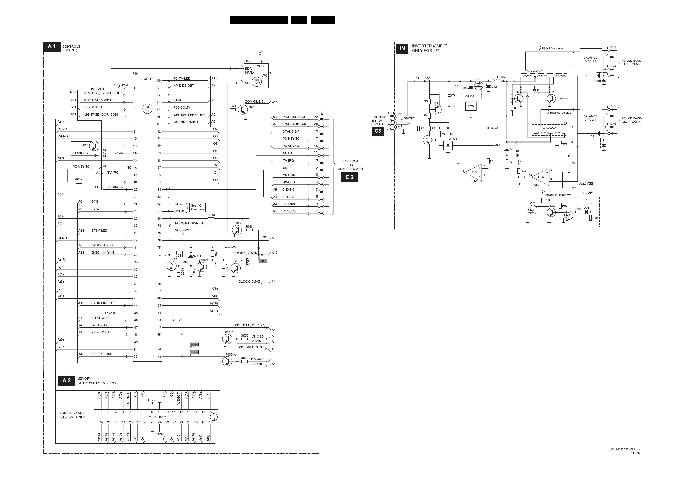
Block Diagrams, Testpoint Overviews, and Waveforms
Block Diagram (TV Control and Inverter Panel)
26LC13E 6.
A1
!
&
''
!"%
")
!"
!
$
%""
"
$
%$
$
#!$
'
'
" "
IN
11
11
! # 0
#
*##
-./
)
1
))
)
1)
)
! -
1
,
)
!
"
!
'
&
"
"
"
"
"
"
"
"
&&
!"#!!
!"
!(
!"
#
"!
"
")
!
"
%"
"
*#
#
!
C5
*#
#
!
C2
"##
!"#
!
88 ""
48.4/8>
!
&&"'
!
#
#
1
)
/23 4567,28
)
/23 4567,28
.57897/5: 9/.9;/7
)
!
""
!
""
1
1
)
!
!"% '
!
!"% '
A2
# + !
# %
!$ !
"
"
"
"
&
"
"
"
"
ERR
15
! '8<=
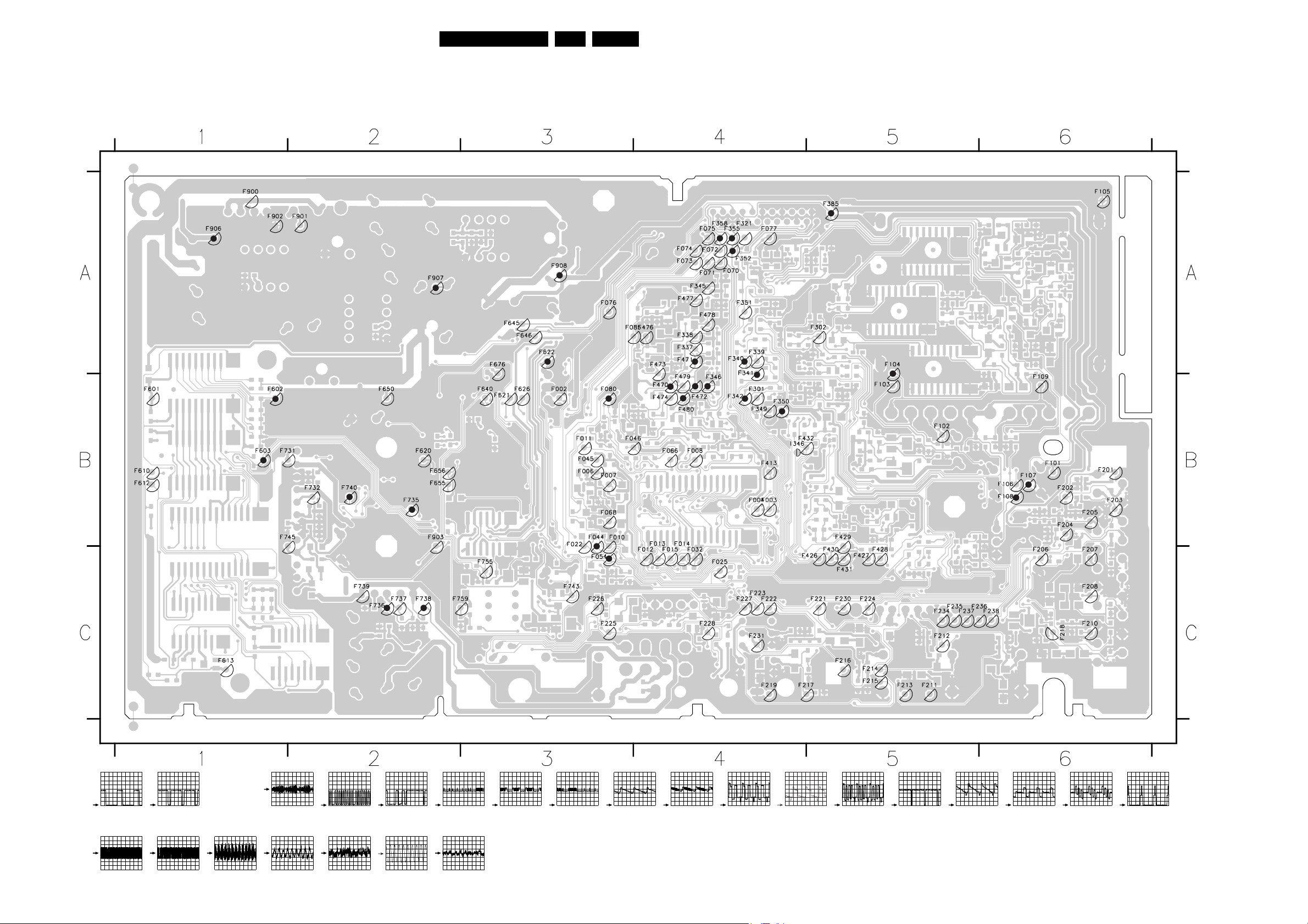
Block Diagrams, Testpoint Overviews, and Waveforms
Testpoint Overview TV Board
F002 B3
F003 B4
F004 B4
F006 B3
F007 B3
F008 B4
F010 B3
F011 B3
F012 C4
F013 B4
F014 B4
F015 C4
F022 B3
F025 C4
F032 C4
F044 B3
F045 B3
F046 B3
F054 C3
F066 B4
F068 B3
F070 A4
F071 A4
F072 A4
F073 A4
F074 A4
F075 A4
F076 A3
F077 A4
F080 B3
F085 A3
F101 B6
F102 B5
F103 B5
F104 A5
F105 A6
F106 B6
F107 B6
F108 B6
F109 B6
F201 B6
F202 B6
F203 B6
F204 B6
F205 B6
F206 C6
F207 C6
F208 C6
F210 C6
F211 C5
F212 C5
F213 C5
F214 C5
F215 C5
F216 C5
F217 C4
F218 C6
F219 C4
F221 C5
F222 C4
F223 C4
F224 C5
F225 C3
F226 C3
F227 C4
F228 C4
F230 C5
F231 C4
F234 C5
F235 C5
F236 C6
F237 C5
27LC13E 6.
F238 C6
F301 B4
F302 A5
F321 A4
F337 A4
F338 A4
F339 A4
F340 A4
F341 A4
F342 B4
F345 A4
F346 B4
F349 B4
F350 B4
F351 A4
F352 A4
F355 A4
F358 A4
F385 A5
F413 B4
F426 C5
F427 C5
F428 C5
F429 B5
F430 C5
F431 C5
F432 B4
F470 B4
F471 A4
F472 B4
F473 A4
F474 B4
F476 A4
F477 A4
F478 A4
F479 B4
F480 B4
F601 B1
F602 B1
F603 B1
F610 B1
F612 B1
F613 C1
F620 B2
F621 B3
F622 A3
F626 B3
F640 B3
F645 A3
F646 A3
F650 B2
F655 B2
F656 B2
F676 A3
F731 B1
F732 B2
F735 B2
F736 C2
F737 C2
F738 C2
F739 C2
F740 B2
F743 C3
F745 B1
F755 C3
F759 C2
F900 A1
F901 A2
F902 A1
F903 B2
F906 A1
F907 A2
F908 A3
I346 B4
F044
1V / div DC
5ms / div
F602
2V / div AC
2ms / div
F054
1V / div DC
20µs / div
F603
2V / div AC
2ms / div
F080 = 2V3 DC
F622
100mV / div AC
5µs / div
F104
500mV / div DC
20µs / div
F735
20mV / div AC
1ms / div
F107
1V / div AC
20µs / div
F736
20mV / div AC
1ms / div
F108
1V / div DC
20µs / div
F738
200mV / div DC
20µs / div
F340
1V / div DC
20µs / div
F740
20mV / div AC
1ms / div
F341
1V / div DC
20µs / div
F906 = 8V3 DC
F907 = 5V4 DC
F908 = 3V5 DC
F342
1V / div DC
20µs / div
F346
1V / div DC
20µs / div
F350
1V / div DC
20µs / div
F352
200mV / div DC
20µs / div
F355
10mV / div AC
1ms / div
F358
200mV / div DC
20µs / div
F385
200mV / div DC
20µs / div
F470
500mV / div DC
20µs / div
F471
500mV / div DC
20µs / div
F472
500mV / div DC
20µs / div
F480
1V / div DC
20µs / div
CL 36532073_009.eps
031203
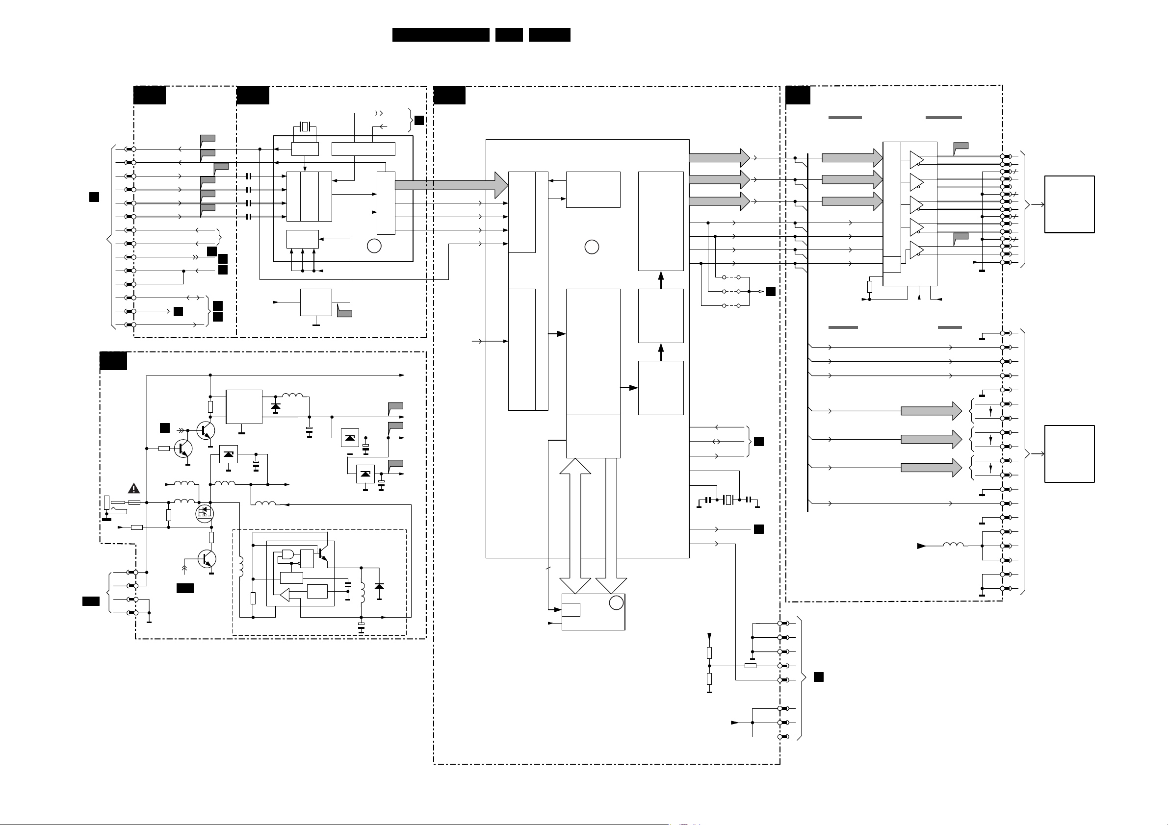
Block Diagrams, Testpoint Overviews, and Waveforms
Block Diagram (Scaler Board)
28LC13E 6.
A1
TO/FROM 1010 TV BOARD
12/24V
DC-IN
TO/FROM
1902 OF TV
BOARD
A10
C1
+5V
10
22
20
19
17
16
14
13
12
POWER
1002
3014
(1)
1003
1
C2
9
7
5
3
1
4
3
2
I/O & INTERFACE
VS-OSD
HS-OSD
AV-CVBS
B-Pb
G-Y
R-Pr
PC-HDAUDIO-L
PC-HDAUDIO-R
STAND-BY
PC-VSYNC
PC-HSYNC
SDA-1
RESET
C5
SCL-1
C2
STAND-BY
3001
5010
+5V
5011
(2)
3015
(1) = FOR 13"/15" ONLY
(2) = FOR 20 " ONLY
PANEL-PWR-CTL
C5
F689
F690
(C-SYNC)
F692
F693
F694
PC-SYNC
3005
7002
(1)
(2)
F691
N.C.
C1
C3
C5
C3
C5
7001
1
VIN
5
ON|OFF
7003
7011(OPTIONAL)
1
(1)
5013
7005
3016
7004
2305
2308
23
C3
2315
OUT
3
5015
(2)
3009/10
FB
2029
5014
8
7
7302
N10
C7
K1
F2
G3
D2
+5
2
4
(2)
7010
VCC
VIDEO DECODER
1301
A3
Sync
AI12
AI32
AI22
AI42
VXDD
Analog Input
Power
Ctrl
VDDE
Video Proc
VDDI
7301
3 2,4
IN
ADJ
5001
6002
2007
(supply for LCD panel)
PAN-VCC
12V
Q
S
R
OSC
REF
6
5
B4
Decoder O/P
+3V3
OUT
1
1
P10 N9
IIC Reg Map
YCBCR
S
VDDA
F304
7009
3
2
3
4
ERR
17
2
2015
1
7006
1
ONLY FOR 20"
2025
5025
2026
SDA-1
SCL-1
XPDO
XPD7
X-PORT
XCLK
12-24DC-SUP
F012
F009
F013
23
2006
6025
12V
XRV
XRH
:
+5
+3V3
+1V8
C2
VIDEO CONVERTER
C5
DA-DATA 0....7
DA-FID
DA-HSYNC
DA-CLK
DA-VSYNC
N.C.
7351
FAROUJA-S2300
PORT
206
208
195
2
8 BIT
YCrCb
INPUT
207
INPUT PROC
AUTO SYNC
AUTO ADJ
PORT
1
24 BIT
YCrCb
INPUT
+3V3
OUTPUT (LVDS)
C4
LVDS-OUT (15")
7501
TXOUT0-
47
TXOUT0+
46
TXOUT1-
45
TXOUT1+
42
TXOUT2-
41
TXOUT2+
38
TXOUT3-
37
TXOUT3+
TTL PARALLEL-TO-LVDS
TXCLKOUT-
TXCLKOUT+
VCC
PLLVCC
40
39
LVDSVCC
F535
PAN-VCC
34 44
+3LVDS+3V3
+3PLL
FSHFCLK
FHSYNC
FVSYNC
R-V-OUT (0-7)
G-Y-OUT (0-7)
B-U-OUT (0-7)
PDE
CLK GEN
PLLs
ERR
16
NR
De-interlace
FRC
SDRAM
Interface
O/P Proc
Sync Gen
DACs
Horizontal
and
Vertical
Enhancers
Horizontal
and
Vertical
Scalers
B-U-OUT (0-7)
(NOT USED)
SOFT-RESET
47
46
45
191
192
2358 2356
SDA-1
SCL-1
FHSYNC
FVSYNC
FDE
FSHFCLK
4391
4392
4393
1351
PC-SYNC
C2
C2
7
4
5
1
2
3
5
1
2
3
4
5
6
7
R-V-OUT (0-7)R-V-OUT (0-7)
G-Y-OUT (0-7)G-Y-OUT (0-7)
B-U-OUT (0-7)
FHSYNC
FVSYNC
FDE
FSHFCLK
3511
TTL-OUT (13" & 20")
27
28
30
31
32
PLL
PWRDWN
1,9,26
F529
48
13M5
DATA 0...31
ADDR 0...10
PANEL-PWR-CTL
BACK-LIGHT-EN
C1
PAN_VCC
5504
9
7352
CLK & CONTROL
TIMING
REG
VDD/VDDQ
SDRAM
2M x 32
ERR
21
+5V
3342
3344
3343
1341
1
2
3
4
5
TO CN1
IN
INVERTER
PANEL
6
12-24DC-SUP
7
8
1506
2
4
10
12
18
20
26
28
LCD
PANEL 15"
34
36
40
1501
1
2
4
5
6
7
15
16
25
26
LCD
PANEL 13" & 20"
35
36
37
38
39
40
41
42
43
CL 36532073_036.eps
111103
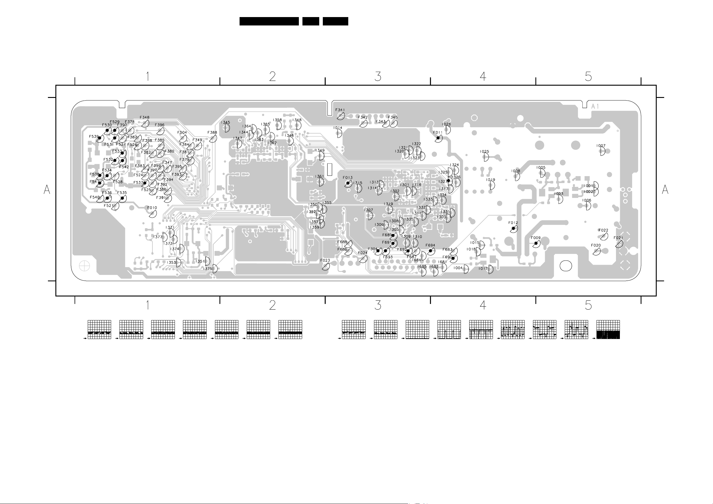
Block Diagrams, Testpoint Overviews, and Waveforms
Testpoint Overview Scaler Board
F009 A4
F010 A1
F011 A4
F012 A4
F013 A3
F020 A5
F021 A5
F022 A5
F023 A2
F024 A3
F304 A3
F341 A3
F342 A3
F343 A3
F345 A3
F347 A1
F348 A1
F349 A1
F378 A1
F379 A1
F380 A1
F381 A1
F382 A1
F383 A1
F384 A1
F385 A1
F386 A1
F387 A1
F388 A1
F390 A1
F391 A1
F392 A1
F393 A1
F394 A1
F395 A1
F396 A1
F397 A1
F398 A1
F399 A1
F504 A1
F521 A1
F524 A1
F525 A1
F526 A1
F527 A1
F528 A1
F529 A1
F530 A1
F531 A1
F532 A1
F533 A1
F534 A1
F535 A1
F536 A1
F537 A1
F538 A1
F539 A1
F540 A1
F541 A1
F542 A1
F683 A4
F686 A3
F687 A3
F688 A3
F689 A3
F690 A4
29LC13E 6.
F691 A3
F692 A3
F693 A3
F694 A3
I001 A5
I002 A5
I003 A5
I004 A4
I005 A5
I006 A5
I007 A5
I008 A4
I014 A3
I015 A4
I017 A4
I018 A4
I019 A4
I025 A4
I026 A4
I301 A3
I302 A3
I303 A4
I305 A3
I306 A3
I307 A3
I308 A3
I309 A3
I310 A3
I311 A3
I313 A3
I314 A3
I315 A3
I316 A3
I317 A4
I319 A3
I320 A3
I321 A3
I322 A3
I323 A3
I324 A4
I325 A4
I326 A4
I327 A4
I331 A4
I332 A3
I333 A3
I334 A4
I335 A3
I344 A2
I345 A2
I346 A2
I347 A2
I348 A2
I349 A2
I350 A2
I351 A1
I352 A2
I353 A1
I355 A3
I357 A2
I358 A2
I359 A2
I361 A2
I362 A2
I363 A2
I364 A2
I365 A2
I371 A1
I373 A1
I374 A1
I375 A1
I377 A1
I681 A4
I682 A4
I684 A3
I685 A3
3139 123 5694.1
F009 = 3V3 DC
F011 = 12V DC
F012 = 5V DC
F013 = 1V8 DC
F304 = 3V3 DC
F529
500mV / div DC
10µs / div
F530
500mV / div DC
10µs / div
F531
F532 F533
500mV / div DC
500mV / div DC
10µs / div
10µs / div
500mV / div DC
10µs / div
F534
500mV / div DC
10µs / div
F535
500mV / div DC
10µs / div
F536
500mV / div DC
10µs / div
F537 = 3V3 DC
F538 = 3V2 DC
F539 = 3V DC
F541
500mV / div DC
10µs / div
F542
500mV / div DC
10µs / div
F689
1V / div DC
5ms / div
F690
1V / div DC
20µs / div
F691
200mV / div DC
20µs / div
F692
200mV / div DC
10µs / div
F693
200mV / div DC
10µs / div
F694
200mV / div DC
10µs / div
I327
1V / div DC
2µs / div
CL 36532073_025.eps
171103
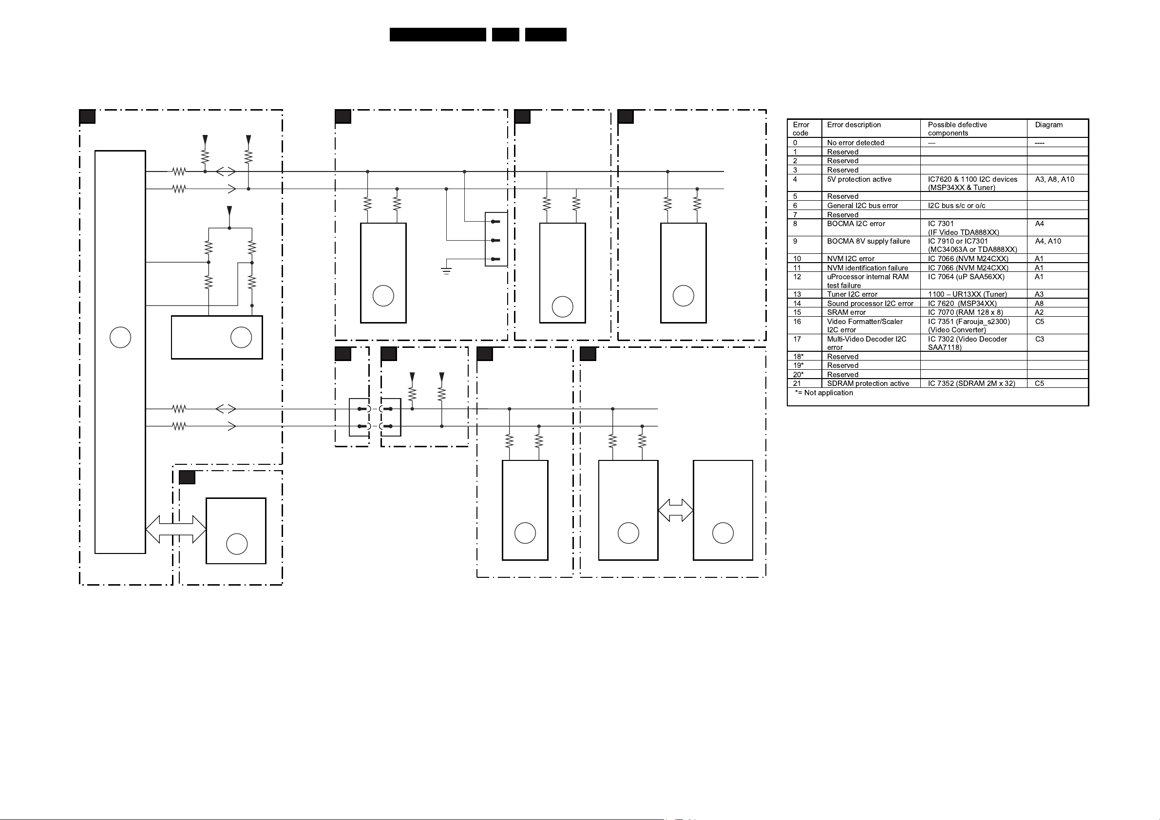
Block Diagrams, Testpoint Overviews, and Waveforms
I2C-IC’s and Error Codes Overview
IIC
A1
7064
SAA5667
U-CONT
ERR
12
82
81
1
78
84
83
+3V5
3085
3017
SDA-NVM
SCL-NVM
7066
M24C32
(NVM)
EEPROM
3018
3019
+3V5
3048
+3V5
3064 3065
3086 3084
56
ERR
10,11
3047
SDA-0
SCL-0
SDA-1
SCL-1
A3
A1
TUNER
3101
54
1100
TUNER
UR1316
ERR
13
C2
1010
14
12
1681
14
12
3100
+5
CONNECTOR
FOR SERVICE
(REACHABLE VIA
HOLE IN REAR
+5
3682
3681
1111
COMPAIR
COVER)
VIDEO
C3
DECODER
30LC13E 6.
IF-VIDEO
A4
3332
1
2
3
18
TDA8885
BOCMA
VIDEO
PROC.
7301
ERR
8
3331
17
C5
VIDEO
CONVERTER
AUDIO
A8
PROCESSING
3620
3621
21
7620
MSP34xx
AUDIO
DECODER
ERR
14
Error codes
Error
code
0 No error detected ----
1 Reserved
2 Reserved
3 Reserved
4 5V protection active IC7620 & 1100 I2C devices
5 Reserved
6 General I2C bus error I2C bus s/c or o/c
7 Reserved
8 BOCMA I2C error IC 7301
9 BOCMA 8V supply failure IC 7910 or IC7301
10 NVM I2C error IC 7066 (NVM M24CXX) A1
11 NVM identification failure IC 7066 (NVM M24CXX) A1
12 uProcessor internal RAM
13 Tuner I2C error 1100 UR13XX (Tuner) A3
14 Sound processor I2C error IC 7620 (MSP34XX) A8
15 SRAM error IC 7070 (RAM 128 x 8) A2
16 Video Formatter/Scaler
17 Multi-Video Decoder I2C
18* Reserved
19* Reserved
20* Reserved
21 SDRAM protection active IC 7352 (SDRAM 2M x 32) C5
*= Not application
Error description Possible defective
test failure
I2C error
error
components
(MSP34XX & Tuner)
(IF Video TDA888XX)
(MC34063A or TDA888XX)
IC 7064 (uP SAA56XX) A1
IC 7351 (Farouja_s2300)
(Video Converter)
IC 7302 (Video Decoder
SAA7118)
Diagram
A3, A8, A10
A4
A4, A10
C5
C3
SRAM
A2
(NOT FOR NAFTA)
CY7C1019CV33
7070
SRAM
ERR
15
3327
P10 N9
7302
SAA7118E
VIDEO
DECODER
ERR
17
3328
3356
46 45
7351
FAROUJAS2300
VIDEO
CONVERTER
ERR
16
3354
7352
K4S643232E
-TC50
SDRAM
2M x 32
ERR
21
CL 36532073_039.eps
171103

Block Diagrams, Testpoint Overviews, and Waveforms
Powerlines Overview
31LC13E 6.
SUPPLY
UNIT
12V 13" 15"
24V 20"
C1
1001-1 1
12_24DC_SUP
POWER
2
STAND-BY
+5
+5
C5
C2
5003
13" 15" (12V) ONLY
5010
20" (24V) ONLY
5011
13" 15" (12V) ONLY
5013
7011 (OPTIONAL)
20" (24V) ONLY
5015
1002
7000mA
7001
50015009
21
7002
7003
CONTROL
7009
23
7006
23
PANEL_PWR_CTR
23
7010
MC34063A
CONTROL
62
+
STABILIZER
5002
CONTROL
5025
4
C5
12_24DC_SUP
7005
5014
5026
12_24DC_SUP
+5V
+3V3
+1V8
PAN_VCC
+12V
1003
+3V3
+1V8
LOCAL SUPPLY
A10
1902
1341
4
3
2
1
7901
CONTROL
STANDBY
8
7
6
5
4
3
2
1
1
2
3
4
1x
3x
+5V
3x
1x
I/O
C2
+5
VIDEO DECODER
C3
7301
+5
+3V3
OUTPUTS (LVDS)
C4
PAN_VCC
+3V3
5517
VIDEO CONVERTOR
C5
+3V3
+1V8
+5V
12-24DC_SUP
5521
5504
3517
3516
3342
3344
+5
5304
23
4301
5354
5351
5352
5353
5357
K4-7302
+3V3
LCD 15"
PANEL
1506
39
LVDS
INPUT
40
LCD 13".20"
1501
PANEL
39
TTL
40
INPUT
41
+3V3
+3 LVDS
+3 PLL
+3V3
DAC_3V3
VDD_IO_3V3
+1V8
DAC_1V8
PLL_1V8
VDD_CORE_1V8
+3V
+5
121-7351
3343
BACK-LIGHT_EN
12_24DC_SUP
1903
11V9
3
2
1600mA
7900
1
INVERTER (FOR 13" ONLY)
IN
CN1
8
Vcc
7
6
ON/OFF
5
OR
4
3
2
1
INVERTER (FOR 15" ONLY)
IN1 IN2
CN1
8
Vin
7
6
ON/OFF
5
OR
4
3
2
1
INVERTER (FOR 20" ONLY)
IN1
CN1
8
Vin
7
6
ON/OFF
5
OR
4
3
2
1
Vbri
Vbri
Vbri
5930
33u
F1
F3A
F1
F3A
F1
F3A
5900
5901
3925
3904
3915
3930
12V
R1Q1R5
12V
R43
R44
7920
6925
CONTROL
AND
STABILIZER
7903,7904
POWER
DOWN
CIRCUIT
7910
CONTROL
AND
STABILIZER
7930
CONTROL
AND
STABILIZER
C3
R3
Q2
R4
R7
R6
D1,Q3
Vin1
R50
Q8
5V 5V
R49
D15
R26
Q11
R25
R50
Q8
R49
Q3
D15
5921
26
5911
27
5931
27
R8 C4,5
Q4-Q6
CONTROL
Va
5V
Vin1
Vin1Vin1
5V
5V
250mA
A1 A9
POWER_DOWN
300mA/400mA
320mA
Q8
D3,8
Vin1
5V
IN2
Vin1
5V
12_24DC_SUP
12_24DC_SUP-1
L2
L1
Vb
1x
1x
5x
+3V5+3V5
4x
+8V3+8V3
7x
+5V4+5V4
U_CONT
A1
+3V5
+5V4
MEMORY
A2
+3V5
TUNER
A3
+5V4
6120, 7120
CONVERTER
IF VIDEO
A4
+3V5
+5V4
+8V3
4303
VIDEO
A5
+5V4
+8V3
COMB
A6
FILTER
+5V4
AUDIO DELAY LINE
A7
+5V4
DC/DC
5301
5601
+3V5
+5V4
+3V5
6101
BZX384-C33
+3V5
+5V4
+8V3
+8V3A
+8V3A
+5V4
+8V3
+8V3A
+5V4
+5VD
+5V4
9-1100
TUNING VOLTAGE
AUDIO PROC.
A8
+5V4
+8V3
AUDIO AMPLIFIER
A9
12_24DC_SUP_1
+3V5
SCART I/O
A11
12_24DC_SUP
+3V5
+8V3
+5V4
FRONT LED
J
1170
2
7
1201
5620
+3V5
+8V3
+5V4
+5V4A
+8V3
+12_24DC_SUP_1
+3V5
12_24DC_SUP
(FOR ITV ONLY)
+3V5
+8V3
+5V4
+8V3
CL 36532073_038.eps
+3V5
4203
1231
2
7
171103

Circuit Diagrams and PWB Layouts
7. Circuit Diagrams and PWB Layouts
TV Board: U_Cont
U_CONT
32LC13E 7.
A
B
C
D
E
F
(COMMON)
1 2 3 4 5 6 7 8 9
PC-HSYNC
A1
KEYBOARD
A11
LIGHT-SENSOR_SDM
A11
OENOT
A2
WENOT
A2
TV-IRQ
A1
STATUS2_SVHS-RR-DET
A11
HIS-OFF
A5
SOUND-ENABLE
A9
A9,A10
HP-SIDE-DET
A9
POWER-DOWN-INT
A1
POWER-DOWN
A10
COMM-LINE
A11
(SCART)
1010
C2
TO 1681 OF SCALER S23 CL BOARD
PC-HDAUDIO-L
22
0V
21
PC-HDAUDIO-R
20
0V
19
STAND-BY
2V9
18
PC-HSYNC
17
0V
PC-VSYNC
16
0V
15
14
4V8
13
5V
12
4V8
11
VS-OSD
10
0V
HS-OSD
9
0V5
8
7
0V6
6
5
0V6
4
3
0V6
2
1
0V6
SDA-1
TV-IRQ
SCL-1
C-SYNC
B-DRIVE
G-DRIVE
R-DRIVE
STAND-BY
A8
A8
F070
F071
A1
F077
F073
A1
F074
A1
F072
A1
A5
A4
A4
A4
3034
A4
A5
100R3021
F080
V-SYNC
H-SYNC
3022
2K2
10K
+3V5
3068
3072
100K
3037
10K
3038
0V6
10K
7008
BFS20
3006
10K
47K
7068
BC847BW
0V
BC847BW
7067
BC847BW
3053
10K
3052
10K
4008
RES
2V9
0V6
4036
RES
7036
0V
3008
10K
+3V5
3036
10K
FOR DIVERSITY TABLE SEE DIAGRAM A2
+3V5
SDA-NVM
3063
2K2
2057
4u7
+3V5
7062
BC847BW
+5V4
0V
3V5
0V
F075
5
SDA
3V5
0V
3014
8K2
+3V5
3069
15K
3070
27K
3071
100K
7069
BC847BW
3V3
F076
VSS
4
+3V5
+5V4
3V5
8
VCC
7066
M24C32
NVM
+3V5
3015
10K
3046
4K7
BZX284-C2V4
F068
3083
470R
7022
BC847BW
3062
47K
6031
3082
10K
+3V5
0V
E0
E1
E2
SCL
WC_
3023
8K2
1SS355
STBY
+3V5
3029
10K
6020
1
2
3
6
3V5
7
WC-NVM
3V5
F085
3081
7063
BC847BW
0V7
2043
4u7
P50-COMM
+3V5
2049
220n
SCL-NVM
F066
+3V5
3099
FOR
SERVICE
3094
10K
4K7
NOT FOR
NTSC &
LATAM
0V
2053
10u
F045
3045
12K
+3V5
2012
RES
3032
10K
3028
47K
+3V5
+3V5
3065
4K7
3084
100R
2045
18p
2010
820p
F003
F002
IO(0)
3055
10K
+3V5
3056
47K
4K7
3064
3V5
3V5
NC
A(14)
3V5
3V5
5V1
NC
0V5
0V
2V7
3V5
5V3
0V2
0V
F046
3V5
7064
5
7
8
10
11
12
13
14
18
17
19
2
95
96
97
99
93
85
98
BC847BS
2018 2n2
18p
3086 100R
2046
(1)
P3.2/ADC2
P3.3/ADC3
A15_LN
A14
_RD
_WR
VSSC
VSSP
P0.5
_EA
P0.2/INT2
P0.1/TX
_PSEN
P3.0/ADC0
P2.3/PWM2
P2.4/PWM3
P2.5/PWM4
VSSC
P2.1/PWM0
AD0
P2.6/PWM5
7053-B
3060
10K
3057
RES
2019
RES
F004
NC
3
1
A17_LN
P0.0/RX
MOVX_WR
P2.7/PWM6
F006
+3V5
3V5
2052
RES
3024
1K
IO(2)
AD2
ROMBK.0
NC
+3V5
+5V4
0V
5V3
94
4
P3.1/ADC1
P2.2/PWM1
I2C-bus,
general I/O
ROM
(128 K/
192 K
BYTES)
ROMBK.1
ROMBK.2
F044
F054
3054
10K
3003
10K
7053-A
BC847BS
F022
RES
3012
A(7)
1516
A7
+5V4
8K2
A(8)
6768
A8
DISPLAY
VSYNC
3V5
+5V4
3013
8K2
3042
150R
F008
NC
0V
3V5
A(12)
47 48
37 38
G
A12
P1.1/T0
P3
0 - 7
P0
0 - 7
P2
0 - 7
MOVX_RD
RESET
_RESET
0V
F007
3044
10K
2055
RES
3V5
0V2
+3V5
3009
0V
A(3)
100
P2.0/TPWM
TV CONTROL
INTERFACE
PROCESSOR
INTERFACE
P3.5/INT5
HSYNC
4V8
3V5
3061
470R
3030
1K
+3V5
+3V5
3066
5042
4u7
8K2
100n2044
100p
IO(1)
IO(7)
0V
3V5
80 81828384
8687 88899909192
R
A3
AD1
AD7
P1.3/TI
AND
MICRO-
3V5
3V5
75 767778 79
VDDP
A16_LN
P1.0/INT1
NC
2V6
P1.1/T0
IO
A0 - A16
MEMORY
VDS
0V1
3058
470R
DATA
CAPTURE
RAMBK.0
5152535455565758 59660616263646566
A(16)
2056
RES
A9
A(9)
5041
4u7
A10
A(10)
+3V5
A11
A(11)
VDDC
VSSC
3V5
F010
3004
8K2
2051
100n
DRAM
(14 KBYTES)
VSSP
_INTD
NC
+5V4
2050
IO(6)
AD6
P3.6
0V
IO(5)
AD5
F025
IO(4)
AD4
3059
150R
IO(3)
AD3
P0.6
28
3V5
2020
RES
F011
3V
4V8
2V8
4V8
P1.4/SCL1
P1.6/SCL0
P1.7/SDA0
P1.5/SDA1
P3.4/PWM7/T2EX
P1
0 - 7
SYNC_FILTER
XTALIN
XTALOUT
OSCGND
70717273 74
69
+3V5
3010
2K2
3088
3050
3018 100R
*
3019
*
3017 100R
(1)
EU & AP-PAL
NTSC-AP
NTSC & LATAM
46
B
45
VDDC
44
43
_COR
42
VPE
41
FRAME
40
A1
39
A2
RAMBK.1
50
NC
49
A0
A(13)
36
A13
35
IREF
34
A(15)
33
A15_BK
32
CVBS1
31
CVBS0
30
VSSA
29
P0.7/T2
27
A4
26
A5
25
P3.7
24
P0.4/INT4
23
A6
22
P0.3/INT3
21
VPE
20
ALE
NC
1057
RES
2042
RES
0V
3V5
3V5
A(1)
A(2)
A(0)
1V3
0V7
A(4)
A(5)
A(6)
100R
100R
100R
100R3085
NC
F012
NC
0V
1V
5V
0V
2041
RES
POWER-DOWN-INT
SDA-1
SCL-1
SAA5667
SAA5645
SAA5647
F015
F014
F013
P50-INT
F032
A1
A1
A1
5040 4u7
2017
3016 1K0
3051 24K
+3V5
F044
1V / div DC
5ms / div
+3V5
+3V5
100n
100n2016
1u02015
1u02014
3035
470R
3049
10K
3007 8K2
4057
3048
+3V5
F054
1V / div DC
+3V5
20µs / div
SEL-MAIN-FRNT-RR
3047
2K22K2
RESRES
20472048
3043
150R
3033
10K
2054
3092 100R
3031
2013
3093
RES
+5V4
8K23002
CLOCK12MHZ
SEL-IF-LL_M-TRAP
FBL-TXT-OSD
SEL-MAIN-R1R2
G-TXT-OSD
(SCART)
STATUS1
PC-TV-LED
R-TXT-OSD
RC5
IO(0:7)
A3,A4,A6,A8
SDA-0
SCL-0
A3,A4,A6,A8
B-TXT-OSD
RES
2021
SVHS-SIDE-DET
A(0:16)
G-SC1-IN_Y-IN
RES
CVBS-TXT-CC
470R
RES
1%
CENOT
SYS2
SYS1
F080 = 2V3 DC
STBY-LED
CL 36532023_004.eps
021203
A5,A8
A4
A5
A11
A11
A4
A11
A2
A4
A11
A2
A11
A6
A2
A6
A6
A4
A11
A5
A4
A
B
C
D
E
F
1010 C1
1057 E7
2010 B4
2012 E3
2013 D9
2014 D8
2015 C8
2016 C8
2017 C8
2018 F4
2019 A4
2020 A7
2021 C9
2041 F8
2042 F7
2043 E3
2044 A6
2045 B4
2046 A4
2047 B9
2048 B9
2049 A3
2050 A6
2051 F6
2052 F5
2053 A3
2054 C9
2055 F5
2056 F6
2057 E2
3002 E8
3003 F5
3004 F6
3006 A2
3007 E9
3008 A2
3009 A5
3010 F7
3012 A5
3013 A5
3014 C2
3015 C2
3016 C8
3017 B7
3018 B7
3019 B7
3021 A1
3022 A1
3023 D3
3024 A5
3028 F4
3029 F3
3030 F5
3031 D9
3032 F4
3033 C9
3034 A1
3035 D9
3036 D2
3037 D2
3038 E2
3042 A5
3043 C9
3044 E5
3045 B3
3046 D3
3047 B9
3048 B9
3049 D8
3050 A7
3051 C8
3052 F2
3053 F2
3054 F5
3055 F4
3056 F4
3057 F4
3058 F6
3059 A7
3060 F4
3061 F6
3062 C3
3063 B2
3064 A4
3065 A4
3066 A6
3068 D1
3069 D2
3070 E2
3071 E2
3072 E1
3081 E3
3082 E3
3083 E3
3084 A4
3085 B7
3086 A4
3088 A7
3092 C9
3093 D9
3094 D3
3099 C3
4008 A2
4036 E2
4057 E9
5040 C8
5041 F6
5042 A6
6020 F3
6031 E3
7008 A2
7022 F3
7036 E2
7053-A F5
7053-B E4
7062 C2
7063 E3
7064 B4
7066 A3
7067 F2
7068 D2
7069 E2
F002 D4
F003 D4
F004 B5
F006 E5
F007 E5
F008 B5
F010 E6
F011 A7
F012 C8
F013 D8
F014 D8
F015 D8
F022 F5
F025 E7
F032 E8
F044 E5
F045 A3
F046 A4
F054 E5
F066 B3
F068 E3
F070 D1
F071 D1
F072 E1
F073 E1
F074 E1
F075 F2
F076 F2
F077 E1
F080 C1
F085 D3
1 2 3 4 5 6 7 8 9

Circuit Diagrams and PWB Layouts
(
(
(
(
(
TV Board: Memory for 100-pg Teletext
1 2
33LC13E 7.
Personal Notes:
A
B
C
MEMORY FOR 100-PG TELETEXT
(COMMON FOR EUROPE & AP-PAL)
A(0)
A(1)
A(2)
A(3)
A(4)
A(5)
A(6)
A(7)
A(8)
A(9)
A(10)
A(11)
A(12)
A(13)
A(14)
A(15)
A(16)
A1
A1
A1
OENOT
WENOT
CENOT
DIVERSITY TABLE DIAGRAM A1 AND A2
3V3
3V3
3V3
3V3
3V3
0V
3V5
0V
0V
3V5
3V4
0V
0V
0V
0V
0V
0V
3V3
3V3
3V3
1
2
3
4
13
14
15
16
17
18
19
20
21
29
30
31
32
28
12
5
2060
100n
0
1
2
3
4
5
6
7
8
9
10
11
12
13
14
15
16
OE
WE
CE
+3V5
5050
4u7
3V5
8
24
VCC
RAM
128Kx8
0
A
128K-1
VSS
9
25
0
DQ
7
2061
100n
7070
CY7C1019CV33
6
7
10
11
22
23
26
27
3V3
0V
0V
0V
0V
0V
0V
0V
2060 A1
2061 A2
5050 A2
7070 A2
A
B
IO(0)
IO(1)
IO(2)
IO(3)
IO(4)
IO(5)
IO(6)
IO(7)
C
NAFTA
AP -/69
V
Latam
AP-NTSC -/61
V
V
Component type
COL) R
COL) R
PHSE) Y
PHSE) Y
PHSE) Y
Europe -/58
Europe -/12
Item#
VV V
2060 -- -- -- CER2 0603 X7R 16V 100N COL
VV V
2061 -- -- -- CER2 0603 X7R 16V 100N COL
VV V
3028 -- -- -- RST SM 0603 47K PM5 COL
VV V
3029 -- -- -- RST SM 0603 10K PM5 COL
VV V
3032 -- -- -- RST SM 0603 10K PM5 COL
VV V
3049 -- -- -- RST SM 0603 10K PM5 COL
VV V
3094 -- -- -- RST SM 0603 10K PM5 COL
VV V
5050 -- -- -- FXDIND SM 0805 4U7 PM10 COL R
VV V
6020 -- -- -- DIO SIG SM BAS316
VV V
7022 -- -- -- TRA SIG SM BC847BW
VV V
7064 -- -- -- IC SM SAA5667HL/M1/
7064 -- -- -- -- -- IC SM SAA5645HL/M1
7064 -- -- -- -- IC SM SAA5647HL/M1
7070 -- -- -- IC SM CY7C1019CV33-15ZC(CYPR)R
VV
V
1 2
CL 36532023_005.eps
150403

Circuit Diagrams and PWB Layouts
TV Board: Tuner Function
TUNER FUNCTION
(13"/15"/20" SCART)
34LC13E 7.
A
B
C
D
E
1 2 3 4 5 6 7 8 9
AP -/61 & Latam
Item#
1100 -- -- TUNER UR1316/A I H-3
1100 -- -- TUNER UR1336/A F S H-3
2108 -- -- -- ELCAP 6V3 S 470U PM20 COL A
2108 -- ELCAP 25V S 100U PM20 COL A
2109 -- -- FIL CER 39MHZ75 MKTGA* BS A
3102 -- -- RST SM 0603 10K PM5 COL
3102 -- -- RST SM 0603 JUMP. 0R05 COL
3103 -- -- RST SM 0603 1K5 PM5 COL
3103 -- -- RST SM 0603 2K2 PM5 COL
3136 -- -- RST SM 0603 100R PM5 COL
6102 -- -- DIO SIG SM BAS316 (COL) R
Europe -/12 & -/58
VV
VV
V
VV
VV
VV
VV
VV
VV
VV
VV
COMPAIR
1111
A1
A1
A8
NAFTA
1
2
3
AP -/69
V
SCL-0
SDA-0
SIF-FM
Component type
3130
1K2
2V7
7130
BFS20
1V8
3131
270R
F105
F107
F108
2V5
PAL / SECAM
NTSC / LATAM
1100
*
12
13
MT
14
15
AS SCL SDA +5V ADC
3100
0R
3101
0R
3132
100K
2130
1n0
7131
BFS20
1n0
(PENDING FOR 12NC)
# LOCALLIB
TUNER
34
5V3
2V6
2101
3133
820R
1V3
0V9
31352131
560R
1100
*
UR1316
UR1336
NC
5678
2V6
5V3
2102
22p22p
+5V4
21323134
100K
1V7
100n
F109
2133
1n0
1
2
NC
9
10
11
1V7
5V3
7V1
F103
0V
0V
F101
F102
(NA used 2142)
2104
47n
F104
4101
RES
(NA used 6148)
BZX384-C33
10u
F104
500mV / div DC
20µs / div
6101
2103
50V
2108
10V470u
F107
1V / div AC
20µs / div
470u
BAS316
2106
6102
6103
RES
3102
10K
+5V4
10V
F108
1V / div DC
5122
12u
2107
100n
20µs / div
3103
1K0
2120
2121
4n7
5120
1m
4n7
7120
BC847BW
DC/DC CONVERTER
4V4
3120
47R
2122
100p
5121
1m
3122
100K
0V4
2125
220p
2126
4n7
For Nafta, different item nos. are used for this circuit:
EU/AP/LT used NA used
2120
2121
2122
2123
2124
2125
2126
3120
3121
3122
5120
5121
6120
7120
F106
AGC
IF-TER
2124
33n
2123
33n
7V4
2144
2143
2145
2146
2147
2148
2149
3144
3146
3145
5149
5148
6149
7149
12V6
A4
A5
3121
27K
6120
BAV99
A
B
C
D
E
1100 B2
1111 C1
2101 D3
2102 D3
2103 C5
2104 C4
2106 C5
2107 C6
2108 D5
2120 A7
2121 A7
2122 A8
2123 A8
2124 A8
2125 B8
2126 B8
2130 E2
2131 E2
2132 E3
2133 E4
3100 C2
3101 D2
3102 D5
3103 B6
3120 A7
3121 A9
3122 B8
3130 D2
3131 E2
3132 E2
3133 E3
3134 E3
3135 E3
4101 E4
5120 A7
5121 A8
5122 B6
6101 B5
6102 C5
6103 C5
6120 B9
7120 B7
7130 E2
7131 E3
F101 B4
F102 C4
F103 C4
F104 C4
F105 B2
F106 C8
F107 C2
F108 D2
F109 C4
CL 36532023_006.eps
1 2 3 4 5 6 7 8 9
021203

Circuit Diagrams and PWB Layouts
35LC13E 7.
TV Board: IF Video Sync Chroma
IF-VIDEO -SYNC-CHROMA
(13"/15"/20" SCART & CINCH EXCEPT CINCH3L)
1
4303
3301
+8V3
RES
A
A5
A5
A3
RES
3305
3325
2301 100n
VIF1
VIF2
AGC
SCART
CINCH AP
3302
4302
*
3304
3303
390R
*3304
100R
220R
B
NAFTA ONLY
2305
2306
VSIF1
A5
C
VSIF2
A5
A8
A8
PIP-AUDIO
SIF-TV
D
CVBS-SC2_MON-OUT
A11
A6
A5
A6
E
A6
A1
A6
A5
A5
A11
F
A11
A11
A11
A5
A5
CVBSOUTA
MAIN-CVBS-EXT-IN
Y-IN
C-IN
CLOCK12MHZ
COMB-ON
Y-HISTOGRAM
Y-MAIN
R-SC1_V-IN
G-SC1-IN_Y-IN
B-SC1-IN_U-IN
(SCART)
FBL-SC1-IN
U-MAIN
V-MAIN
F346
1 2345678
RES
RES
3349
100R
F302
330p
4n7
2349
1V9
1V9
1V7
2302
22n
3346
1K0
2V4
2351
I346
15
1u0
5301
+8V3A
6u8
7301-A
*
PLLIF
1 IFIN1
IFIN22
7 AGCOUT
3306
3K9
2307
4n7
+8V3
8V5
2V
1u0
1u02348
10n2347
2346
10n
PLL VIDEO DEMOD
10u
2
PAL / SECAM
NAFTA
AP-NTSC / LATAM
IF AMPLIFIER
AFC
CALIBRATION
AGC
AGC + NARROW
BAND AUDIO FM
PLL DEMODULATOR
DE-EMPHASIS
10
2308
4u7
35V
EU ONLY
2V6
HC-49/U
4301
3347
100R
F351
F350
F349
1330
12MHZ
F345
SIF19SIF2
SIFAGC
2V4
2310
16V
3348
10R
7330
BC847BW
2344
33p
8
1V9
1V9
2V6
26 CVBS2OUT
54 CVBS1OUT
2V5
24 CVBSINT
3V8
29 CVBS|Y2
3V4
3V6
20 C3
1V4
2345
33p
7301
*
TDA8885
TDA8887
TDA8889
SWITCHABLE
SOUND TRAPS
4.5 / 5.5 / 6 / 6.5
SECPLL
2V3
2309
220n
7301-B
CVBS|Y321
7V8
23
VP1
MHZ
3308
100R
EU ONLY
QSSO|AMOUT
1128
2V6
2311
220n
3307
RES
CVBS
SWITCH
VIDEO
IDENT
3
DECDIG6GND
50
2321
100n
57
IREF
5
3V9
2V8
2V5
17
SCL
SDA
IIC BUS
RGB
OUTPUT
CALIBRATION
BLKIN
3V2
2336
2337
F352
200mV / div DC
F321
VCS
4
3V8
18
2335
820p
CONTROL
DECBG
55
5V
2312
VIDEO
AMPLIFIER
MUTE
OUTPUT
+
VOLUME
4V
RES
2313
100n
IFVO
IFVO|AUDOUT
16
2V9
12VIDEO|SIF
27
3V
3311
1K0
F340
1V / div DC
20µs / div
F341
1V / div DC
20µs / div
54
5326
2u7
4324
7V8
2V
6327
7V8
2V2
2326
220p
+8V3A
2327
120p
3309
10R
2314
1u0
3313
10R
2315
1u0
2316
BAS316
1u0
+8V3A
3315
470R
680R3316
4V9
22
SWO160SWO2
+8V3A
3310
100R
3314
1K0
3326
4325
2304
10u 16V
2V9
75R
NAFTA
ONLY
3312
1K0
2V6
BC847BW
3327
1K0
3328
1K5
7302
BC847BW
7303
+3V5
2303
100n
NC
F342
1V / div DC
20µs / div
678 9
3317
2319
7301-C
PH1LF59
EHTO3
15K
3319
10K
NC
2318
3V9
2V2
+8V3A
4n7
3318
27K
100n
F346
2317
1u0 50V
SYNC
SEPARATOR
VERTICAL
SYNC
SEPARATOR
GND1 GND2
25
F301
1V / div DC
20µs / div
2320
2n2
SW OUT
CD
MATRIX
SATURATION
CONTROL
MATRIX
WHITE /
BLACK
STRETCH
LUM-
DELAY
PEAKING
CORING
Y
RGB-2
INPUT
RGB / YUV
MATRIX
Y
U
V
INPUT
U
V
2V1
YIN40YOUT
3V4
R|2
470n
2341
2V6
2V6
G|2
41
470n
2342
0V
2V6
BL|2
B|2
43
470n
2343
100R
3345
10p
2340
+3V5
10K
3344
42
UI|BI
UO|BL3
VO|YI|GI
47
45 48
46
2V4
2V3
3343
VI|RI
2V4
2V4
2339
100n
8K2
NAFTA ONLY
WHSTR
1939
3V5
F342
R|1
35
3V4
F341
FSCOUT
49
U
V
BASE
BAND
DELAY
LINE
CHROMA
BAND-
PASS CATHODE
+TRAP
PAL / NTSC /
SECAM
DEMODULATOR
OSCIN52OSCOUT
1V6
51
1V6
4V1
HALFT
RGB
+
RGB1
+
TINT
G|1
36
3V4
CONTROL
61
13
B|1
37
3V4
F340
3342
F350
1V / div DC
20µs / div
2V1
58
PH2LF
VCO
BL|1
3844
0V3
F339
0V8
FBISO
+
3324
39K
CONTROL
R
G
B
30
100R3340
100R3341
100R
20µs / div
8V2
53
VP2
HORIZONTAL
3329
270K
22n
22n
22n2338
5302
6u8
2325
16V10u
3V5
14
LPST-UP
OUTPUT
VERTICAL
OUTPUT
E / W
OUTPUT
3V3
3V3
3V3
BCLIN
F355
200mV / div DC
20µs / div
3320
3323
H-DRIVE 56
EW-DRIVE 62
+8V3
3350
10R
3333
150R
R
33
32G
B
31
34
3V3
F338
F337
4320
4323
DR+ 63
DR- 64
2350
1u0
+5V4
3336
RES
F358
200mV / div DC
20µs / div
RES
RES
BC847BW
3V3
2330
15p
BC847BW
3V3
2331
15p
BC847BW
3334 150R
3V3
150R
3335
BC847BW
0R
3360
RES
3338
100R3339
0V1
3331
7350
2332
15p
7360
2361
+8V3
2V2
7353
7356
16V100u
2322
100n
8V
+3V5
3337
RES
3322
3K3
2V7
2V7
2V7
2324
100p
2360
U-HISTOGRAM
1n
CVBS_TER_OUT
1K03330
100R
100R3332
V-HISTOGRAM
9
SC
5303
6u8
+8V3
3321
3K3
LINEDRIVE1
V-SYNC
+8V3
(SCART)
OUTSEL
SCL-0
SDA-0
R-DRIVE
F352
3352
150R
3351 470R
G-DRIVE
F355
3355
150R
3354
470R
B-DRIVE
F358
470R
3358
150R
3357
10K
BAS316
2K4 1%
6360
3361
3362
FBL-TXT-OSD
B-TXT-OSD
G-TXT-OSD
R-TXT-OSD
CL 36532073_001.eps
BAS316
6361
RES
021203
A5
A5
A1
A11
A6
A1
A1
A1
A1
A1
BAS316
6362
A1
A1
A1
A1
A5
A5
A
B
C
D
E
F
1330 E2
2301 A1
2302 B1
2303 A5
2304 A5
2305 C1
2306 C1
2307 C1
2308 C2
2309 C2
2310 C2
2311 C3
2312 C3
2313 C4
2314 A5
2315 B5
2316 C5
2317 A7
2318 A6
2319 C6
2320 A7
2321 A7
2322 A9
2324 A9
2325 A8
2326 B5
2327 C5
2330 D9
2331 D9
2332 E9
2335 F8
2336 F8
2337 F8
2338 F8
2339 F6
2340 F6
2341 F5
2342 F5
2343 F5
2344 E2
2345 E2
2346 E1
2347 E1
2348 E1
2349 E1
2350 C9
2351 D1
2360 E9
2361 F9
3301 A1
3302 A1
3303 A1
3304 A1
3305 B1
3306 C1
3307 C3
3308 C3
3309 A5
3310 A5
3311 A5
3312 B5
3313 B5
3314 C5
3315 B6
3316 C6
3317 A6
3318 C6
3319 C6
3320 A8
3321 A9
3322 B9
3323 A8
3324 C7
3325 A1
3326 A5
3327 C5
3328 C5
3329 C8
3330 C9
3331 C9
3332 C9
3333 D8
3334 D9
3335 E9
3336 E8
3337 B9
3338 F8
3339 F8
3340 F7
3341 F7
3342 F7
3343 F6
3344 F6
3345 F6
3346 D1
3347 D2
3348 D2
3349 E1
3350 C9
3351 C9
3352 C9
3354 D9
3355 D9
3357 E9
3358 E9
3360 F9
3361 E9
3362 F9
4301 C2
4302 A1
4303 A1
4320 A9
4323 A9
4324 A5
4325 A5
5301 A1
5302 A8
5303 A9
5326 A5
6327 C5
6360 E9
6361 E9
6362 E9
7301-A A1
7301-B D2
7301-C A6
7302 A5
7303 B5
7330 D2
7350 C9
7353 D9
7356 D9
7360 E9
F301 C7
F302 A1
F321 A8
F337 F8
F338 F8
F339 F7
F340 F7
F341 F7
F342 F7
F345 F2
F346 F1
F349 D2
F350 D2
F351 D2
F352 C9
F355 D9
F358 D9
I346 D1

Circuit Diagrams and PWB Layouts
(
TV Board: SAW Filter, Ext. Video Select, Histogram, & C-Sync Generator
SAW FILTER, EXT. VIDEO SELECT, HISTROGRAM & C-SYNC GEN
(13"/15"/20" EUROPE & AP-PAL)
1 2 3 4 5 6 7 8 9
EXT. VIDEO SELECT
A
B
C-SC2_SVHS-IN
A11
C-FRONT-IN
A11
Y-CVBS-FRONT-IN
A11
CVBS-SC1_AV1-IN
A11
Y-CVBS-SC2_AV2-IN
A11
A1
A1
C
"401" ~ "425"
+8V3A
IF-TER
A3
D
5452
390n
SEL-IF-LL_M-TRAP
A1
E
F
VIDEO & QSS IF
"451" ~ "470"
+8V3
7401
74HC4053
16
SWITCH
8V2
6
VCC
G3
14
3V8
2408
100n
MUXDX
12
1y0
13
1y1
2
1
5
3
15
2y0
2y1
4
3y0
3y1
GND
VEE
8
7
4451
4452
4453
4454
4455
3404
3405
3403
3401
0R
3402
SEL-MAIN-FRNT-RR
SEL-MAIN-R1R2
5451
6u8
2453
10n
3456
2K2
3457
7452
27K
BC847BW
0V
3458
18K
0V
0R
0R
0R
0R
1SS356
4V9
RES
3410
RES
3409
6451
3455
6K8
2404 22n
2403 1u0
2401 1u0
3461
2K2
22n2405
1u02402
1SS356
3459
22K
7451
BC847BW
3465
47K
2452
10n
3460
2K2
6452
RES
4456
4457
4458
4459
4460
EUROPE & AP
PAL-MUTLI
ONLY
1 2 3 4 5 6 7 8 9
+8V3 +8V3
5V3
11
+8V3
5V3
10
9
5V3
2407
100n
2
I
3
ISWI
1
4
5
6
9
GND
10
13
14
15
18
2
I
3
ISWI
1
4
5
6
9
10
GND
13
14
15
18
2
I
3
ISWI
1
4
5
6
9
10
GND
13
14
15
18
3411
1K5
10u 16V
3412
220n
1K5
7412-A
BC847BS
3414
1K5
2415
3415
220n
1K5
7412-B
BC847BS
1452
OFWK9656L
40M4
1453
OFWK9656L
40M4
1454
OFWK9656L
40M4
2417
3V6
3V6
NC
NC
NC
BAS316
BAS316
O1
O2
O1
O2
O1
O2
64122412
3413
6415
1K0
8V5
11
12
16
17
11
12
16
17
11
12
16
17
2V9
2V9
7
8
7
8
RES
5453
820n
7
8
5454
RES
8V2
3417
10R
F413
3416
1K0
3418
10R
2419
1u0
4462
2418
1u0
4461
C-SYNC GENERATOR
"380" ~ "399"
HISTOGRAM PROCESSING
2470
100n
F474
36LC13E 7.
3380
22K
+8V3
0V5
RES
SATURATION
COMPENSATION
NON-LINEAR
AMPLIFIER
HISTOGRAM
PROCESSOR
7V7
0V5
6380
BAS316
2390
2n2
3473
3476
15K
F476
3390
4K7
3472
0R
20
BLM
STRETCH
AMPSEL
VCC16VEE
NLC
4
+8V3+8V3
3393
3394
1V2
27K
7390
BC847CW
2471
2472
10n
10n
F472F470 F471
AMPSEL
UIN2 UOUT 19
1V6
VIN3 VOUT 18
1V6
INPUT
YIN7
1V8
0V6
+8V3A
SC5
7403
TDA9171
5470
AMP
TIMING
AND
CTRL
6u8
3392
220K
4K7
0V5
6390
BAS316
3470
10K
220K3471
F473
5V 1V7
61
TAUHM
AMPSEL
HISTOGRAM
MEASUREMENT
HM19HM210HM311HM412HM5
10n
2474
2475 10n
2391
330p
8
2476 10n
3391
10K
3V3
7391
BC847CW
2473 220n
13
10n2477
10n
2478
F385
200mV / div DC
3389
560R
RES
3475
0V5
BLUE
OUTPUT
AMP
SUPPLY
AND
BIASING
15
17
10u
2479
20µs / div
0V6
2380
470p
0V2
0V5
BLG
VREF
5V
2480
10u
F413
1V / div DC
20µs / div
+5V4+5V4 +5V4
3381
5K6
3382
0V2 0V
10K
7380
BC847CW
+5V4 +5V4
10K 2K7
0V5
7383
BC847CW
3474
0R
2V4
2V4
YOUT 14
2481
100n
2V1
F477
3477
18K
6472
BAS316
6470
RES
F478
F479
6471
RES
F470
500mV / div DC
20µs / div
2V3
7381
BC847CW
0V
7384
BC847CW
+8V3A
7V8
BC847BW
0V6
3478
10K
3479
47K
BC847BW
RES
33883387
7471
3383
4K7
3482
3480
47K
RES
7472
10K
0V8
F471
500mV / div DC
3384
4K7
2382
220n
BC847BW
20µs / div
7382
BC847CW
7385
BC847CW
7473
0V
F472
500mV / div DC
20µs / div
MAIN-C-EXT-IN
MAIN-CVBS-EXT-IN
H-SYNC
+5V4
5V3
3385
1V7
3386
560R
LINEDRIVE1
4470
4471
4472
F480
SANDCASTLE1
3481
4K7
3484
2482
100p
10K
3483
10K
0V6
"471" ~ "499"
2381
1u0
C-SYNC
470R
F385
Y-MAIN
V-MAIN
U-MAIN
U-HISTOGRAM
V-HISTOGRAM
Y-HISTOGRAM
SC
+5V4
3485
10K
HIS-OFF
VIF2
VIF1
VSIF1
VSIF2
F480
1V / div DC
20µs / div
A6
A4,A6
A1
A1
3395
270R
A4
A4
A4
A4
A4
A4
A4
A4
A6
A1
A4
A4
A4
A4
CL 36532023_008.eps
A
B
C
D
E
F
021203
1452 D3
1453 E3
1454 F3
2380 B7
2381 A9
2382 C8
2390 C6
2391 B5
2401 B1
2402 B1
2403 A1
2404 A1
2405 A1
2407 C3
2408 C2
2412 A3
2415 B3
2417 A3
2418 A4
2419 B4
2452 D2
2453 D1
2470 D4
2471 D4
2472 D5
2473 D6
2474 F5
2475 F5
2476 F5
2477 F6
2478 F6
2479 F6
2480 F7
2481 F7
2482 F9
3380 A6
3381 A7
3382 A7
3383 A8
3384 A8
3385 A9
3386 A9
3387 B7
3388 B8
3389 C7
3390 B6
3391 B6
3392 B5
3393 B5
3394 B5
3395 A9
3401 B1
3402 B1
3403 A1
3404 A1
3405 A1
3409 B1
3410 B1
3411 A3
3412 A3
3413 B3
3414 B3
3415 B3
3416 C4
3417 A4
3418 B4
3455 D1
3456 D1
3457 E1
3458 E1
3459 E2
3460 D2
3461 D1
3465 E2
3470 D5
3471 D5
3472 D6
3473 D6
3474 D7
3475 D7
3476 F6
3477 F7
3478 E8
3479 E8
3480 E8
3481 E9
3482 F8
3483 F9
3484 E9
3485 E9
4451 C2
4452 D2
4453 D2
4454 D2
4455 D2
4456 F2
4457 F2
4458 F2
4459 F2
4460 F2
4461 D4
4462 D4
4470 D9
4471 D9
4472 E9
5451 C1
5452 D1
5453 E4
5454 F4
5470 F5
6380 B6
6390 C5
6412 A3
6415 B3
6451 D1
6452 D2
6470 E7
6471 E7
6472 F7
7380 A7
7381 A8
7382 A8
7383 C7
7384 C8
7385 C8
7390 C5
7391 C6
7401 A2
7403 F5
7412-A B3
7412-B C3
7451 E2
7452 E1
7471 D8
7472 F8
7473 E8
F385 A9
F413 B4
F470 D4
F471 D4
F472 D5
F473 D5
F474 E4
F476 F6
F477 E7
F478 E7
F479 E8
F480 E9
NAFTA
Europe
AP-PAL
V
AP-NTSC/Latam
V
V
V
V
V
VV
V
V
V
V
V
VV
V
V
V
V
V
V
V
V
V
Component type
RHM0) R
Item#
V
1452 -- -- -- FIL SAW SM 38MHZ9 OFWK3953L R
1452 -- -- FIL SAW SM 45MHZ75 OFWM1967L R
1452 -- -- -- FIL SAW SM 38MHZ9 OFWK7265L R
1454 -- -- -- FIL SAW SM 38MHZ9 OFWK9656L R
V
1454 -- -- -- FIL SAW SM 38MHZ9 OFWK9361L R
VV
2452 -- CER2 0603 X7R 50V 10N COL
2453 -- CER2 0603 X7R 50V 10N COL
V
3455 -- -- RST SM 0603 6K8 PM5 COL
V
3456 -- -- RST SM 0603 2K2 PM5 COL
V
3457 -- -- RST SM 0603 27K PM5 COL
V
3458 -- -- RST SM 0603 18K PM5 COL
V
3461 -- -- RST SM 0603 2K2 PM5 COL
V
4451 -- RST SM 0603 JUMP. 0R05 COL
4453 -- -- -- RST SM 0603 JUMP. 0R05 COL
V
4455 -- -- RST SM 0603 JUMP. 0R05 COL
V
4457 -- -- RST SM 0603 JUMP. 0R05 COL
V
4458 -- -- -- RST SM 0603 JUMP. 0R05 COL
4460 -- -- -- RST SM 0603 JUMP. 0R05 COL
V
5451 -- -- FXDIND SM 1008 6U8 PM5 COL R
V
5452 -- -- FXDIND SM 0805 0U39 PM10 COL R
5452 -- -- FXDIND SM 0805 0U82 PM10 COL R
V
6451 -- -- DIO SIG SM 1SS356
V
7452 -- -- TRA SIG SM BC847BW (COL) R

Circuit Diagrams and PWB Layouts
TV Board: Analog Comb Filter
ANALOG COMB FILTER
(13"/15"/20" SCART & CINCH EXCEPT CINCH3L)
37LC13E 7.
Personal Notes:
A
B
C
MAIN-CVBS-EXT-IN
A5
+5V4
5426
6u8
2426
16V10u
+5V4
5427
6u8
1
234
+8V3A
2424 C1
2426 B1
2428 B1
2429 C1
2430 D2
A
2431 A2
2432 A2
2433 D3
2434 E3
2435 E3
3426 B1
3427 C2
3428 A2
3429 A2
3430 A3
3428
1K0
2431
RES
3429
10R
2432
1u0
7V8
2V
3431
1K0
2V7
7427
BC847BW
3430
100R
CVBSOUTA
CVBS-TXT-CC
A4
A1
3431 A2
3432 C4
3433 D4
3434 D4
B
C
3436 E4
3437 E4
4426 B3
4427 B3
5426 B1
5427 C1
7405 B2
7427 A3
7428 E4
F403 E1
F407 E1
F408 E1
F409 D3
F410 D3
F411 D3
F412 D4
3426
1K0
2428
1u0
1V7
12 Y|CVBS1
0V9
0V7
7405
TDA9181
2 INPSEL
3 Y|CVBS2
1CIN
7SC
CLAMP
CLAMP
SAND-
CASTLE
4426
RES
5V3
FILTER
TUNING
4427
RES
5V3
6
VCC
2H/4H DELAY
ADAPTIVE
COMB FILTER
CLOCK
VDD
GEN
Y-IN
A4
5
Y|CVBSO
14
1V4
C-IN
1V4
16COUT
RES
3432
A4
D
E
2424
16V
10u
MAIN-C-EXT-IN
A5
2429
47n
3427
1K0
AGND
DGND
13
49
0V
2430
100n
2
F429
FSC8FSCSEL
0V8
F430
34
SYS110SYS2
11
0V
F431
2435
47n
5V
2433
100p
2434
100p
OUTSEL
15
F432
+8V3A
7V9
3V5
3436
1K0
0V
3433
100R
3434
100R
7428
BC847BW
4V1
SANDCASTLE1
OUTSEL
SYS2
SYS1
COMB-ON
3437
100R
CL 36532073_002.eps
A4
D
A1
A1
A4
E
A5
031203

Circuit Diagrams and PWB Layouts
TV Board: Audio Delay Line
AUDIO DELAY LINE
(COMMON)
38LC13E 7.
B
C
D
E
F
+5V4
GNDDIGITAL
2V3
GNDDIGITAL
2V3
+5VD
5V3
GNDDIGITAL
5V3
2V3
+5VD
5V3
7601
TC74HC590AF
14
EN3
13
12
11
10
CT=0
7602
14
EN3
13
12
11
10
CT=0
TC74HC590AF
123
5601
F601
16
5V3
8
GNDDIGITAL
9
4
5V3
15
1
2
3
4
5
6
7
16
5V3
8
GNDDIGITAL
9
4
15
1
2
3
4
5
6
7
+5VD
+5VD
2601
100n
GNDDIGITAL
2V6
2V6
2V6
2V6
2V6
2V6
2V6
+5VD
GNDDIGITAL
4601
4602
4603
7603
CY62256
+5VD
5V3
2603
100n
GNDDIGITAL
2602
100n
2V6
2V6
2V6
2V6
2V6
2V6
(1)
2V6
GNDDIGITAL
2V5
11
I|O0
28
VCC
A021A1
(1)
4605
4604
GNDDIGITAL
2V5
2V5
2V5
2V5
2V5
2V5
I|O112I|O213I|O315I|O416I|O517I|O618I|O7
A224A325A426A51A62A73A84A9
23
(1) NOT USED
(1)
4606
GNDDIGITAL
GNDDIGITAL
2V5
19
1u0
COUNTER
C2
G1
CTR8
(CT=255)Z4
1+
C2
G1
CTR8
(CT=255)Z4
1+
COUNTER
VCC
GND
2D 3
VCC
GND
2D 3
GNDDIGITAL
20
CE_
A10
6
5
GNDHOT
4
2V3
22
27
OE_
WE_
A117A128A139A14
GND
10
14
GNDDIGITAL
56789
1
11
2
3
4
5
6
7
8
9
+5VD
20
5V3
EN
C1
1D
10
GNDDIGITAL
F603
2605
100n
GNDDIGITAL
19
18
17
16
15
14
13
12
(1) NOT USED
2V / div AC
2ms / div
4610
4611
4612
4613
4614
4615
4616
4617
(1)
(1)
(1)
(1)
(1)
(1)
F602
(1)
2V6
GNDDIGITAL
F603
GNDDIGITAL
I2S_DATA_IN
2612
330p
I2S_DATA_OUT
2613
470p
I2S_CLOCK
F610
A8
A8
A8
F612
2V3
+5VD
3610
470R
7610
BC847BW
0V2
2611
82p
F613
3611
47K
1
11
2V6
2
3
4
5
6
7
8
9
+5VD
20
5V3
EN
C1
1D
10
GNDDIGITAL
2604
100n
GNDDIGITAL
19
18
17
16
15
14
13
12
2V3
D-LATCH D-LATCH
7604
74HCT573D
2V3
2610
82p
7605
74HCT573D
GNDDIGITAL
F602
2V / div AC
2ms / div
AA
B
C
D
E
F
2601 B2
2602 D2
2603 B2
2604 B7
2605 B8
2610 F6
2611 F6
2612 D9
2613 D9
3610 F5
3611 F6
4601 E2
4602 E2
4603 F2
4604 F2
4605 F2
4606 F2
4610 C9
4611 C9
4612 C9
4613 C9
4614 C9
4615 C9
4616 C9
4617 C9
5601 A1
7601 A1
7602 D1
7603 A2
7604 B7
7605 B8
7610 F6
F601 A1
F602 C9
F603 D9
F610 F9
F612 F5
F613 F6
GNDDIGITAL
1
2
3
456789
GNDDIGITAL
CL 36532023_010.eps
021203

TV Board: Audio Processing
(
(
(
(
(
(
AUDIO PROCESSING
(COMMON)
3691
330R
2624
15p
12p
2647
2640
2633
2635
2636 1u0
4647
4646
4648
4649
2637
2638
1K03645
2689
2690 1u0
F622
100mV / div AC
5µs / div
2633 B2
2634 B2
2635 C2
2636 C2
2637 C2
1u0
1u0
2634
1u0
RES
A
B
C
D
E
1620 E7
1691 A1
2620 A10
2621 A2
2622 A1
2691
22n
A3
A1
A1
A4
A4
A11
A11
A11
A11
A11
A11
A1
A1
2623 B1
2624 A1
2625 B1
2626 B2
2627 B2
1691
TPS
SIF-FM
SCL-0
SDA-0
2622
27p
F622
SIF-TV
2625
180p
PIP-AUDIO
R-SC1_AV1-IN
L-SC1_AV1-IN
R-SC2_AV2-IN
L-SC2_AV2-IN
R-FRONT-IN
L-FRONT-IN
PC-HDAUDIO-R
PC-HDAUDIO-L
AUD_SW
2628 C2
2629 C2
2630 C2
2631 D2
2632 D2
1 2 3 4 5 6 7 8 9 10
1O3
I
G
2
4691
5621
15u
56p2623
3622 2K2
3640 1K0
3633
1K0
3634 1K0
1K03635
3636 1K0
1K03637
3638 1K0
F645
3646 1K0
F646
Circuit Diagrams and PWB Layouts
2638 D2
2639 B2
2640 B2
2645 B7
2646 B7
100R3620
3621 100R
+5V4A
3623
RES
7622
RES RES
4620
3624
RES
F640
2639
2627
220p
4n7
1u0
2629 2630
4n7
1u0
1u0
2631 2632
4n7
1u0
2684
1n0
1V5
1
2
2V5
0V
50
51
1V5
2V8
2652 C8
2653 C8
2654 A7
2655 A8
2656 E5
RES
3626
7620
*
MSP3410G
I2C-CL
I2C-DA
ANA-IN2+52
ANA-IN1+
ANA-IN-
MONO
MONO-IN47
SC1-IN-R45
SC1-IN-L44
SCART 1
SC2-IN-R42
SC2-IN-L41
2621
3625
RES
2628
4n7
7621
F626
RES
2647 B1
2648 A8
2649 B8
2650 C7
2651 E6
2626
47p
3V8
3V8
3V8
3V8
3V8
F621
SCART 2
4n7
3V8
SC3-IN-R39
3V8
SC3-IN-L38
SCART 3
4n7
3V8
3V8
2677
4n7 4n7
SC4-IN-R36
SC4-IN-L35
SCART 4
2678
5859642213
DIVERSITY FOR SOUND IC 7620
MSP-3410G NICAM VERSION W/O VIRTUAL DOLBY
MSP-3420G NTSC VERSION W/O VIRTUAL DOLBY
MSP-3411G NICAM VERSION WITH VIRTUAL DOLBY
MSP-3421G NTSC VERSION WITH VIRTUAL DOLBY
*
2657 B7
2658 B7
2661 C8
2662 C7
2663 D8
NC
NC
9
7
ADR-DA
ADR
ADR-CL
interface
8
ADR-WS
DEMODULATOR
IDENT
A/D
A/D
NC
141524
NC
2664 D8
2665 D8
2666 E8
2667 E8
2668 E7
NC
57
NC
60
AUD-CL-OUT
2688
2669 E7
2670 C8
2671 C8
2672 D9
2673 D9
0V
61
D-CTR-IO1
FM1
FM2
NICAM A
NICAM B
IDENT
SCART-L
SCART-R
2u2
NC
D-CTR-IO0
S1...4
SCART
DACM-SUB
23
0V4
F656
2674 E9
2675 E9
2676 B8
2677 D2
2678 D3
I2SL/R
DSP
Switching Facilities
TESTEN
ADR-SEL
53
62
2656
1n0
2679 B7
2680 E6
2681 E6
2682 E6
2683 E7
5
NC
12
I2S-DA-O1
I2S-DA-IN2
I2S
I2SL/R
LOUDSPEAKER R
LOUDSPEAKER L
HEADPHONE R
HEADPHONE L
SCART-R
SCART-L
ASG043ASG140ASG2
AVSS
48
2V6
37
2684 A3
2688 E4
2689 D2
2690 D2
2691 A1
6
2V6
I2S-DA-IN1
interface
AHVSS
33
+5V4A
3
I2S-CL
2680
2681
2V5
39LC13E 7.
3620 A2
3621 A2
3622 B1
3623 A2
3624 B2
4
NC
I2S-WS
D/A
D/A
D/A
D/A
D/A
D/A
TP56VREF127VREF2
19
NC
470p
100n
3625 B2
3626 A3
3633 B1
3634 B1
3635 C1
31
8V5
AHVSUP
LOUDSPEAKER
HEADPHONE
STANDBYQ
DVSS11DVSUP
63
10
0V
5V3
+5V4A
2651
100n
2682
3p3
RESETQ
DACM-R
DACM-L 21
VREFTOP
AGNDC
CAPL-M
CAPL-A
DACA-R 17
DACA-L 18
SC1-OUT-R 28
SC1-OUT-L 29
SCART 1
SCART 2
SC2-OUT-R 25
SC2-OUT-L 26
XTAL-IN54XTAL-OUT
AVSUP
49
2V5
1620
DSX840
18M432
3636 C1
3637 C1
3638 D1
3640 B1
3645 D1
55
2V5
3V8
3V8
3V8
3V8
16
20
0V4
0V4
46
2V6
34
3V8
32
7V
30
2683
3p3
5V2
2668
1n0
F676
100n
2657
3646 D1
3650 A7
3651 C9
3652 C9
3653 D10
6650
BAS316
F655
2654
220n
1n02645
2646
1n0
2658
10u
16V
NC
10u
+5V4A
2650
3650
22K
2655
10u 16V
2679
100n
16V
2662
1n0
4650
RES
4651
RES
2669
1n0
3654 D10
3655 E9
3656 E9
3691 A1
4620 A2
2648
1u0
2649
1u0
2676
10u
16V
2652
100n
F650
4646 C1
4647 C1
4648 C1
4649 C1
4650 D7
2653
16V
22u
2661
1n0
100n
2664
1u0
2665
1u0
2666
1u0
2667
1u0
2670 1u0
2671
2663
NC
5650
1u0
3V8
3V8
3V8
3V8
16
VCC
MUXDX
1y0
1y1
2y0
2y1
3y0
3y1
5680 C9
6650 A7
7620 A3
7621 A2
7622 A2
1u0
7674 7675
PDTC124ET PDTC124ET
100R
3651
0V4
100R3652
+8V3
5680
4u7
SWITCH
7680
74HC4053
6
G3
14
3V8
11
15
3V8
5V3
10
4
9
GND
8
4651 D7
4691 A1
5620 A9
5621 A1
5650 A8
FOR SCART ONLY
8V5
12
13
2
1
5
3
VEE
7
NC
2674
1u0
2675
1u0
+5V4
7674 B9
7675 B10
7676 C10
7677 D10
7678 E9
+8V3
5620
1u0
0V
2672
1u0
2673
1u0
7678
PDTC124ET
3655
100R
3656
100R
0V4
7676
PDTC124ET
0V3
3653
100R
3654
100R
0V3
7679 E10
7680 D9
F620 A10
F621 A3
F622 A1
I2S_DATA_OUT
I2S_DATA_IN
F620
2620
10u
16V
PDTC124ET
0V3
SEL-MAIN-R1R2
PDTC124ET
0V3
L-CL_VL-OUT
R-CL_VL-OUT
I2S_CLOCK
+5V4A
AUDIO-R
AUDIO-L
R-SC1_AV-OUT
L-SC1_AV-OUT
7677
7679
F626 A2
F640 B2
F645 D1
F646 D1
F650 A8
OUT_MUTE
L-SC2-OUT
R-SC2-OUT
A7
A7
A7
A9
A9
A9
A11
A11
A11
A11
A1
A11
A11
F655 A7
F656 E5
F676 B7
A
B
C
D
AP-PAL Non-VD 15"/20"
NAFTA/AP-NTSC/Latam 15"/20"
Europe Non-VD 13"/15"/20"
Item#
2663 -- -- -- CER2 0603 X7R 16V 100N COL
2664 -- -- -- CER2 0603 Y5V 10V 1U COL
2665 -- -- -- CER2 0603 Y5V 10V 1U COL
2666 -- -- -- CER2 0603 Y5V 10V 1U COL
2667 -- -- -- CER2 0603 Y5V 10V 1U COL
2672 -- -- -- CER2 0603 Y5V 10V 1U COL
2673 -- -- -- CER2 0603 Y5V 10V 1U COL
V
2674 -- -- CER2 0603 Y5V 10V 1U COL
V
2675 -- -- CER2 0603 Y5V 10V 1U COL
3653 -- -- -- RST SM 0603 100R PM5 COL
3654 -- -- -- RST SM 0603 100R PM5 COL
V
3655 -- -- RST SM 0603 100R PM5 COL
E
V
3656 -- -- RST SM 0603 100R PM5 COL
5680 -- -- -- FXDIND SM 1008 4U7 PM5 COL R
V
7620 -- -- IC SM MSP3420G-QI-B8-V3
VV
7620 -- IC SM MSP3410G-QI-C12
7676 -- -- -- TRA SIG SM PDTC124ET
7677 -- -- -- TRA SIG SM PDTC124ET
V
7678 -- -- TRA SIG SM PDTC124ET
V
7679 -- -- TRA SIG SM PDTC124ET
7680 -- -- -- IC SM 74HC4053PW (PHSE) R
Component type
MIAS)Y
MIAS) Y
COL) R
COL) R
COL) R
COL) R
1 2 3 4 5 6 7 8 9 10
CL 36532023_011.eps
140104

Circuit Diagrams and PWB Layouts
TV Board: Audio Amplifier
AUDIO AMPLIFIER
40LC13E 7.
A
B
C
D
E
F
A11
A11
A11
A11
A11
A8
A8
A8
A1
A10
A1
LED_IN
IR_IN
STBY-LED
STATUS
IR_OUT
AUD_SW
AUDIO-L
AUDIO-R
SOUND-ENABLE
POWER-DOWN
STAND-BY
1
FOR ITV
1232
1
2
3
4
5
6
HMLINK
1702
1
25
36
SPPH4
4
F735
20mV / div AC
1ms / div
F740
20mV / div AC
1ms / div
2735
1n0
3735
F735
F740
5V3
2V3
3V3
2V9
3V3
2V9
27K
2740
1n0
3740
27K
7732-A
74LCV08AD
1
2
7732-B
74LCV08AD
4
F755
5
3V5
7732-C
74LCV08AD
9
10
7732-D
74LCV08AD
12
13
QUAD 2-INPUT AND GATE
+3V5
32
1730
3732
220K
2736
1u0
3736
6K8
2741
1u0
3741
6K8
3746
5K6
3V5
14
3
3V5
7
14
6
7
14
8
3V5
7
14
11
7
3V5
3743
1K0
4567
1733
YKC21-3416
3
2752 10u
4740
*
2757
1n5
6755
0V
BAS316
10u2750
50
1750
*
3752
50
1752
*
4738
*
4737
*
4739
*
3759
1K0
3733
RES
2737
4n7
2742
4n7
3745
3K3
F743
2
6731
BZX284-C6V8
6732
BZX284-C6V8
2732
50V10u
2745
50V100u
0V7
2746
50V1u0
1
F732
AN7522N
F745
2785
1n0
GNDEARTH
GNDEARTH
+3V5
7744
BC847BW
1V4
1V4
2V7
4K7
7731
6 CH1-IN
8 CH2-IN
9VOL
2731
33n
3744
0V
12-24DC-SUP_1
5
2V9
STB
GNDCH111GNDCH2
GNDINP
3
7
GNDHOT
1
5733
22u
F731
VCC
11V8
2733
220n
CH1-
3755
100R
2734
10CH2-
12CH2+
16V1m0
2CH1+
4
3756
RES
6V2
6V1
6V1
6V1
2755
1u0
2754
1n5
3757
10K
2758
1n5
+3V5
3V5
3758
4K7
2756
1n5
7756
BC847B
120R3750
470R
8
2789
10n
3760
4K7
F759
3761
2K2
HP-SIDE-DET
OUT_MUTE
2751
470p
2788
10n
2753
470p
2787
10n
A1
A8
2784
4n7
9
2783
4n7
F738
4
F737
3
F736
F739
2786
10n
F736
20mV / div AC
F738
50mV / div AC
17316
5
4
2
3
7
8
9
1
HEADPHONE
1732
2
1
1ms / div
1ms / div
CL 36532073_003.eps
021203
A
B
C
16 OHMS / 3 W
D
E
F
1232 A1
1702 A1
1730 A4
1731 A9
1732 B9
1733 A4
1750 A7
1752 B7
2731 D5
2732 B4
2733 B5
2734 B6
2735 B3
2736 B3
2737 C4
2740 C3
2741 C3
2742 C4
2745 D4
2746 F4
2750 A7
2751 B8
2752 A7
2753 B8
2754 C6
2755 E6
2756 C7
2757 C7
2758 C6
2783 A9
2784 A9
2785 D4
2786 C9
2787 C9
2788 C8
2789 C8
3732 B3
3733 B4
3735 B3
3736 C3
3740 C3
3741 C3
3743 F4
3744 F5
3745 D4
3746 D3
3750 A7
3752 A7
3755 E6
3756 E6
3757 E6
3758 E7
3759 E7
3760 E8
3761 E8
4737 C7
4738 B7
4739 C7
4740 C7
5733 A5
6731 A4
6732 A4
6755 E7
7731 B5
7732-A D3
7732-B E3
7732-C E3
7732-D F3
7744 F4
7756 F7
F731 B5
F732 B4
F735 C2
F736 C9
F737 C9
F738 C9
F739 C9
F740 C2
F743 F4
F745 C4
F755 E3
F759 E8
1
32
4
5
6
7
98

TV Board: Local Supply
Circuit Diagrams and PWB Layouts
41LC13E 7.
A
B
C
D
E
F
1
12-24DC-SUP
1904
1
1902
4
3
2
1
EH-B
FROM 1003 OF SCALER 23 CL BD
A9
F900
11V9
F902
12-24DC-SUP_1
5900
12u
STAND-BY
2
3456
LOCAL SUPPLY
(COMMON)
F901
5901
100MHz 220R
2900
100n
F903
11V9
7900
SI2301DS-T1
3900
1K
2V9
3904
220K
3903
15K
3
2
1
6V
3901
1K
0V
7901
PDTC114ET
2903
10n
0V5
11V9
1903
1600mA F
3925
10R
0V
7903
BC847B
3905
220K
5930
33u
+3V5
6925
SS14
3906
22K
2V3
7904
BC847B
3915
1R0
3920
RES
3910
RES
3930
1R0
3921
1R0
2920
470u 25V
3911
1R0
2910
470u
25V
3931
1R0
3922
RES
3912
1R0
1K
2912
RES
1K
2932
1K
2922
RES
3913
1%
3932
1%
RES
3923
1%
11V7
11V8
11V7
11V8
11V
11V1
1V2
1V2
1V3
7910
MC34063A
DCOL8
IS7
6
VCC
CIN-5
5K6
2914 4n7
7930
MC34063A
DCOL8
IS7
6
VCC
CIN-5
2934
7920
MC34063A
DCOL8
IS7
6
VCC
CIN-5
1K8
2924 4n7
3K3
3914
3933
3924
IPK
OSC
1%
IPK
OSC
1%
IPK
OSC
1%
4n7
QRS
REFERENCE
REGULATOR
QRS
REFERENCE
REGULATOR
QRS
REFERENCE
REGULATOR
SWC 1
SWE
TIMC 3
SWC 1
SWE 2
TIMC 3
GND 4
SWC 1
SWE 2
TIMC 3
GND 4
2
4GND
11V7
11V7
11V
8V4
0V7
5V5
0V7
3V6
0V7
78
1902 C1
1903 C3
1904 C1
2900 C2
2903 F3
2910 B4
2911 A7
2912 B5
2913 B7
A
2914 B5
2920 E4
2921 E7
2922 E5
@
2911
470p
5911
220u
6910
SS14
2923 E7
2924 E5
2931 C7
2932 C5
F906
+8V3
@
@
2913
470u
16V
2999
1m0 16V
,300mA / 430mA
B
2933 D7
2934 D5
2998 D7
2999 B7
3900 C2
3901 D3
3903 F2
3904 E2
F906 = 8V3 DC
F907 = 5V4 DC
F908 = 3V5 DC
3905 E3
3906 E4
3910 A4
3911 A4
3912 A5
3913 B5
3914 B5
3915 A4
3920 E4
3921 E4
3922 E4
2931
470p
5931
220u
6930
SS14
C
3923 E5
3924 E5
3925 E3
3930 C4
3931 C4
3932 C5
3933 C5
2933
470u
10V
F907
+5V4
@@
2998
1m0
16V
,320mA
5900 C2
D
5901 C2
5911 A7
5921 E7
5930 C4
5931 C7
6910 A7
6920 E7
6925 E4
6930 C7
2921
470p
5921
220u
2923
1m0
6.3V
6920
SS14
F908
+3V5
E
,250mA
7900 C2
7901 D3
7903 F3
7904 F4
7910 A5
7920 D5
7930 B5
F900 C1
F901 C2
F902 C1
POWER-DOWN
A1,A9
F903 D2
F906 B7
F907 C7
F908 E7
F
1
2
3
4
CL 36532073_004.eps
567
200104
8

TV Board: SCART I/O
Circuit Diagrams and PWB Layouts
42LC13E 7.
A
B
C
D
E
F
A8
A8
A8
A8
A4
A1
A1,A4
A4
A4
+8V3
A4
A5
1231
TO 1170 OF
FRONT CONTROL
1234
TO 1500 OF
TOP CONTROL
1234
R-SC1_AV-OUT
R-SC1_AV1-IN
L-SC1_AV-OUT
L-SC1_AV1-IN
B-SC1-IN_U-IN
STATUS1
G-SC1-IN_Y-IN
R-SC1_V-IN
FBL-SC1-IN
3225 10R
CVBS_TER_OUT
F221
1
2
F222
3
4
5
6
F224
7
1
2
F223
3
4
BC847B
3228
100R
CVBS-SC1_AV1-IN
PC-TV-LED
0V
4203
*
LIGHT-SENSOR_SDM
3V5
8V2
KEYBOARD
3V5
NC
VOLVOL+
CHCH+
7224
1V9
SCART IO
BZX384-C12
3219
BZX384-C12
8V5
A1
+3V5
A1
+8V3
A1
2V4
2V
1V4
1V
6218
47u 25V
1V3
2224
A1
STBY-LED
A1
RC5
RES
2218
RES
2222
6211
3222
100R
RES
2225
1201
100R
3218
75R
3221
75R
1
3202
220K
3204
47K
3207
220K
3209
47K
RES
2211
3214
6K8
RES
2217
3224
1K0
3255
270R
6250
BZX384-C5V1
7260
BC847BW
4201
2201
330p
2203
330p
2206
330p
2208
330p
2214
330p
3223
68R
FOR ITV
3260
270R
2250
4u7
3261
4K7
3262
5K6
4202
150R3201
3203
150R
3206
150R
3208
150R
3212
100R
3211
75R
3213
22K
3217
100R
3216
75R
1211
4
7261
74HCT1G86
6284
2254
100n
1204
RES
RES
6285
3
1202
1203
1205
1206
1207
1208
RES
2227
3263
5K6
5
2
1
EX-OR
1209
RES
6290
RES
6291
3227
100R
6283
3226
75R
RES
3257
RES
6292
RES
RES
6288
RES
6289
6286
6287
1212
6257
F201
F202
F203
F204
F205
F206
1223
F207
1224
F208
F210
F218
1210
F225
F226
100R3256
F227
+8V3
3258
BZX384-C3V3
3K9
3259
5K6
F230
6281
6282
STBY-LED
6227
6228
F228
1
2
3
4
5
6
7
8
9
10
11
12
13
14
15
16
17
18
19
20
21
RES
RES
LED_IN
IR_IN
IR_OUT
SCART_1
1260
A9
A9
A9
BZX284-C6V8
STATUS
A9
BZX284-C6V8
A9
56
F217
RES
6243
1218
RES
6244
SVHS
1267-A
YKF51-5347
LOCALLIB (242202604926 PI=2)
1269
LPR6520-P210G
TESTLANDS USED IN LC03
F211
F213
F234
TO 1232 (RJ 12) OF SHT A9
F235
8
3
7
2
1
6
5
4
3
2
1
F216
F236
1221
F237
4
9
4299
6
5
1267-B
YKF51-5347
10
11
F219
F238
1220
F231
6207
6208
F215
1217
F212
1214
F214
1216
78
3244
3243
75R
3248
75R
RES
6253
RES
6254
RES
6238
RES
6239
100R
3249
100R
3241
22K
3233
150R
3238
150R
2244
RES
2249
RES
2242
330p
2233
330p
2238
330p
C-SC2_SVHS-IN
Y-CVBS-SC2_AV2-IN
+5V4
3242
10K
STATUS2_SVHS-RR-DET
4242
R-SC2_AV2-IN
3234
47K
L-SC2_AV2-IN
3239
47K
CL 36532073_005.eps
A5
A5
A1
A8
A8
011203
A
B
C
D
E
F
1201 E2
1202 A3
1203 A3
1204 B3
1205 B3
1206 B3
1207 C3
1208 C3
1209 D3
1210 D4
1211 D3
1212 E4
1214 E7
1216 F7
1217 D7
1218 B6
1220 C6
1221 C6
1223 B4
1224 B4
1231 E1
1234 F1
1260 D5
1267-A C5
1267-B C6
1268-1 F5
1268-2 E5
1269 C5
2201 A3
2203 A3
2206 B3
2208 B3
2211 B2
2214 C3
2217 C2
2218 C2
2222 D2
2224 D2
2225 D2
2227 E3
2233 E8
2238 F8
2242 D8
2244 B8
2249 C8
2250 E3
2254 E3
3201 A3
3202 A2
3203 A3
3204 A2
3206 A3
3207 B2
3208 B3
3209 B2
3211 B3
3212 B3
3213 C3
3214 C2
3216 C3
3217 C3
3218 C2
3219 C2
3221 D2
3222 D2
3223 D3
3224 D2
3225 D1
3226 E4
3227 E3
3228 D1
3233 E7
3234 E8
3238 E7
3239 F8
3241 D7
3242 D8
3243 B7
3244 A7
3248 C7
3249 C7
3255 E2
3256 E4
3257 F3
3258 F4
3259 F4
3260 E2
3261 E3
3262 F3
3263 E3
4201 F2
4202 F2
4203 E1
4242 D8
4299 B6
6207 C7
6208 D7
6211 B2
6218 C2
6227 F4
6228 F4
6238 F7
6239 F7
6243 B7
6244 B7
6250 E2
6253 E7
6254 E7
6257 F4
6281 D4
6282 E4
6283 B4
6284 D3
6285 D3
6286 D4
6287 D4
6288 C4
6289 C4
6290 B3
6291 B3
6292 B4
7224 D1
7260 F2
7261 F3
F201 A4
F202 A4
F203 A4
F204 A4
F205 A4
F206 B4
F207 B4
F208 C4
F210 C4
F212 E7
F214 E7
F215 D7
F217 A7
F218 C4
F221 E1
F222 E1
F223 F1
F224 F1
F225 E4
F226 E4
F227 F4
F228 F4
F230 F4
F231 C7
1234
5678

Circuit Diagrams and PWB Layouts
43LC13E 7.
Layout TV Board (13”/15”) (Overview Top Side)
1010 A3
1057 B4
1100 A1
1111 B1
1201 C2
1206 B1
1208 C1
1231 C2
1232 C4
1234 C3
1260 C1
1267 C3
1269 C2
1330 A3
1620 B4
1691 B4
1702 C4
1730 C4
1731 C3
1732 C5
1733 C4
1750 C5
1752 C5
1902 A6
1903 A5
1904 A5
2010 B3
2016 C3
2017 C3
2018 C4
2019 C4
2020 C4
2021 C3
2041 B4
2042 B4
2043 B4
2044 B4
2045 B4
2046 B3
2049 B4
2052 C4
2053 B4
2055 C4
2057 B4
2103 B2
2104 B2
2106 B1
2108 B1
2120 B2
2121 B2
2122 B2
2123 B2
2124 B2
2125 B2
2126 B2
2211 B1
2217 C1
2218 C1
2224 C1
2250 C3
2303 B3
2304 B2
2308 A2
2310 B2
2312 A3
2315 B3
2317 A2
2319 A2
2321 A3
2325 A3
2326 B2
2330 B3
2331 B3
2332 B3
2351 B3
2360 B3
2361 B3
2412 C2
2415 C2
2417 B2
2418 B2
2419 C2
2424 B3
2426 B2
2429 B3
2430 B2
2433 B2
2434 B2
2435 C2
2448 B2
2449 B2
2473 A4
2474 A4
2475 A4
2476 A4
2477 A4
2478 A4
2479 A3
2480 A3
2481 A3
2620 B4
2621 B4
2622 A4
2623 A4
2624 A4
2625 A4
2627 B4
2628 A4
2629 B5
2630 A5
2631 A5
2632 B5
2633 B4
2634 A4
2635 B5
2636 A4
2637 A5
2638 B5
2639 B4
2640 B4
Part 1
CL 36532073_07a.eps
2645 B5
2646 B5
2647 B4
2648 B5
2649 B5
2650 B5
2652 B5
2653 B5
2654 B5
2655 B5
2656 B5
2657 B5
2658 B5
2661 B5
2662 B5
2664 C4
2665 C4
2666 C4
2667 C4
2668 B5
2669 B5
2670 B5
2671 B5
2672 C4
2673 C4
2674 B5
2675 B5
2676 A4
2677 B5
2678 B5
2679 B4
2680 B4
2681 B4
2682 B4
2683 B4
2684 B4
2689 B5
2690 A5
2691 B4
2732 B5
2733 B5
2734 A5
2735 B5
2740 B5
2741 B5
2742 B5
2745 C5
2746 C4
2750 C5
2752 C5
2753 C5
2756 C5
2757 C5
2900 A5
2903 A5
2910 A5
2912 A6
2913 A6
2914 A6
2920 A4
2923 A4
2932 A5
2933 A5
2934 A5
2998 A5
2999 A6
3002 C3
3006 B3
3007 C3
3008 B3
3010 B3
3014 B3
3015 B3
3016 C3
3018 B4
3019 B3
3021 B3
3022 B3
3023 B4
3029 B3
3033 C3
3034 B3
3042 C3
3043 C3
3044 C4
3045 B3
3046 B3
3049 B3
3051 C3
3052 A3
3053 A3
3055 A3
3056 A3
3057 C4
3059 C4
3060 C4
3062 B3
3063 B3
3064 B3
3065 B3
3070 B4
3071 B4
3084 B4
3086 B3
3099 C3
3102 B1
3120 B2
3121 B2
3122 B2
3211 B1
3212 B1
3216 C1
3217 C1
3218 C1
3219 C1
3225 C1
3228 C1
3255 C2
3260 C2
3301 A4
3307 B3
3312 B3
3313 B3
3314 B3
3318 A2
3319 A2
3325 A4
3326 B2
3329 A2
3333 B3
3334 B3
3335 B3
3336 A3
3337 A3
3338 B3
3346 B3
3347 B3
3348 B2
3360 B3
3361 B3
3362 B3
3411 C2
3412 C2
3413 B2
3414 B2
3415 C2
3416 C2
3417 B2
3418 C2
3432 C3
3433 B2
3434 B2
3436 C2
3437 B2
3620 B4
3621 B4
3622 A4
3623 B4
3624 B4
3625 A4
3626 B4
3633 B4
3634 A4
3635 B5
3636 A4
3637 A4
3638 B5
3640 B4
3645 A4
3646 A4
3650 B4
3651 B5
3652 B5
3653 C4
3654 C4
3655 B5
3656 B5
3691 B4
3732 B5
3733 B5
3735 B5
3736 B5
3740 B5
3741 B5
3752 C5
3900 A5
3901 A5
3903 A5
3904 A5
3905 A5
3906 A4
3910 A6
3911 A6
3912 A5
3913 A6
3914 A6
3915 A6
3920 A4
3921 A4
3922 A4
3925 A5
3930 A5
3931 A5
3932 A5
3933 A5
4008 B3
4057 B4
4302 A4
4303 A4
4324 B2
4325 B2
4449 B2
4463 C2
4464 B2
4465 C2
4466 B2
4620 B4
4646 A4
4647 A4
4648 A4
4649 A4
4691 B4
4738 C5
5042 B4
5120 B2
5121 B2
5122 B2
5301 A4
5302 A3
5303 A2
5326 B2
5426 B2
5427 B2
5451 B1
5470 A4
5620 B4
5621 A4
5650 B5
5733 A5
5900 A5
5901 A5
5911 A6
5921 A4
5930 A5
5931 A5
6101 B2
6102 B1
6103 B1
6120 B2
6211 B1
6218 C1
6284 C1
6285 C1
6288 C1
6289 C1
Part 2
CL 36532073_07b.eps
6290 B1
6291 B1
6360 B3
6361 B3
6362 B3
6412 C2
6415 C2
6650 B5
6731 C4
6732 C4
6910 A6
6920 A4
6925 A4
6930 A5
7008 B3
7022 B3
7053 C4
7062 B3
7064 B3
7066 B4
7120 B2
7261 C4
7301 A3
7303 B3
7330 B3
7360 B3
7401 C2
7403 A3
7405 B2
7412 C2
7428 B2
7620 B4
7621 B4
7622 A4
7674 B5
7675 B5
7676 C4
7678 B5
7679 B5
7680 C4
7731 B5
7900 A5
7901 A5
7903 A5
7904 A5
7910 A6
7920 A4
7930 A5
3139 123 5712.2
Part 3
CL 36532073_07c.eps
Part 4
CL 36532073_07d.eps
CL 36532073_007.eps
111103

Circuit Diagrams and PWB Layouts
Layout TV Board (13”/15”) (Part 1 Top Side)
44LC13E 7.
Part 1 of
3139 123 5712.2
CL 36532073_07a.eps
141003

Circuit Diagrams and PWB Layouts
Layout TV Board (13”/15”) (Part 2 Top Side)
45LC13E 7.
Part 2 of
3139 123 5712.2
CL 36532073_07b.eps
141003

Circuit Diagrams and PWB Layouts
Layout TV Board (13”/15”) (Part 3 Top Side)
46LC13E 7.
Part 3 of
3139 123 5712.2
CL 36532073_07c.eps
141003

Circuit Diagrams and PWB Layouts
Layout TV Board (13”/15”) (Part 4 Top Side)
47LC13E 7.
Part 4 of
3139 123 5712.2
CL 36532073_07d.eps
141003

Circuit Diagrams and PWB Layouts
Layout TV Board (13”/15”) (Overview Bottom Side)
48LC13E 7.
Part 1
CL 36532073_08a.eps
Part 2
CL 36532073_08b.eps
3139 123 5712.2
Part 3
CL CL 36532073_08c.eps
Part 4
CL 36532073_08d.eps
CL 36532073_008.eps
281103

Circuit Diagrams and PWB Layouts
Layout TV Board (13”/15”) (Part 1 Bottom Side)
49LC13E 7.
Part 1 of
3139 123 5712.2
CL 36532073_08a.eps
141003

Circuit Diagrams and PWB Layouts
Layout TV Board (13”/15”) (Part 2 Bottom Side)
50LC13E 7.
Part 2 of
3139 123 5712.2
CL 36532073_08b.eps
141003

Circuit Diagrams and PWB Layouts
Layout TV Board (13”/15”) (Part 3 Bottom Side)
51LC13E 7.
Part 3 of
3139 123 5712.2
CL 36532073_08c.eps
141003

Circuit Diagrams and PWB Layouts
Layout TV Board (13”/15”) (Part 4 Bottom Side)
52LC13E 7.
Part 4 of
3139 123 5712.2
CL 36532073_08d.eps
141003

Circuit Diagrams and PWB Layouts
Layout TV Board (20”) (Overview Top Side)
1010 A3
1057 B4
1100 A1
1111 B1
1201 C2
1206 B1
1208 C1
1231 C2
1232 C4
1234 C3
1260 C1
1267 C3
1269 C2
1330 A3
1620 B4
1691 B4
1702 C4
1730 C4
1731 C3
1732 C5
1733 C4
1734 C5
1750 C5
1752 C5
1902 A6
1903 A5
1904 A5
2010 B3
2016 C3
2017 C3
2018 C4
2019 C4
2020 C4
2021 C3
2041 B4
2042 B4
2043 B4
2044 B4
2045 B4
2046 B3
2049 B4
2052 C4
2053 B4
2055 C4
2057 B4
2103 B2
2104 B2
2106 B1
2108 B1
2120 B2
2121 B2
2122 B2
2123 B2
2124 B2
2125 B2
2126 B2
2211 B1
2217 C1
2218 C1
2224 C1
2250 C3
2303 B3
2304 B2
2308 A2
2310 B2
2312 A3
2315 B3
2317 A2
2319 A2
2321 A3
2325 A3
2326 B2
2330 B3
2331 B3
2332 B3
2351 B3
2360 B3
2361 B3
2412 C2
2415 C2
2417 B2
2418 B2
2419 C2
2424 B3
2426 B2
2429 B3
2430 B2
2433 B2
2434 B2
2435 C2
2448 B2
2449 B2
2473 A4
2474 A4
2475 A4
2476 A4
2477 A4
2478 A4
2479 A3
2480 A3
2481 A3
2620 B4
2621 B4
2622 A4
2623 A4
2624 A4
2625 A4
2627 B4
2628 A4
2629 B5
2630 A5
2631 A5
2632 B5
2633 B4
2634 A4
2635 B5
2636 A5
2637 A5
2638 B5
2639 B4
2640 B4
2645 B5
2646 B5
2647 B4
2648 B5
2649 B5
2650 B5
2652 B5
2653 B5
2654 B5
2655 B5
2656 B5
2657 B5
2658 B5
2661 B5
2662 B5
2664 C4
2665 C4
2666 C4
2667 C4
2668 B5
2669 B5
2670 B5
2671 B5
2672 C4
2673 C4
2674 B5
2675 B5
2676 A4
2677 B5
2678 B5
2679 B4
2680 B4
2681 B4
2682 B4
2683 B4
2684 B4
2689 B5
2690 A5
2691 B4
2732 B5
2734 B5
2735 B5
2738 C5
2739 C5
2740 C5
2741 C5
2742 B5
2743 C5
2744 C5
2745 B5
2746 C4
2799 B5
2900 A5
2903 A5
2910 A5
2912 A6
2913 A6
2914 A6
2920 A4
2923 A4
2932 A5
2933 A5
2934 A5
2998 A5
2999 A6
3002 C3
3006 B3
3007 C3
3008 B3
3010 B3
3014 B3
3015 B3
3016 C3
3018 B4
3019 B3
3021 B3
3022 B3
53LC13E 7.
3023 B4
3029 B3
3033 C3
3034 B3
3042 C3
3043 C3
3044 C4
3045 B3
3046 B3
3049 B3
3051 C3
3052 A3
3053 A3
3055 A3
3056 A3
3057 C4
3059 C4
3060 C4
3062 B3
3063 B3
3064 B3
3065 B3
3070 B4
3071 B4
3084 B4
3086 B3
3099 C3
3102 B1
3120 B2
3121 B2
3122 B2
3211 B1
3212 B1
3216 C1
3217 C1
3218 C1
3219 C1
3225 C1
3228 C1
3255 C2
3260 C2
3301 A4
3307 B3
3312 B3
3313 B3
3314 B3
3318 A2
3319 A2
3325 A4
3326 B2
3329 A2
3333 B3
3334 B3
3335 B3
3336 A3
3337 A3
3338 B3
3346 B3
3347 B3
3348 B2
3360 B3
3361 B3
3362 B3
3411 C2
3412 C2
3413 B2
3414 B2
3415 C2
3416 C2
3417 B2
3418 C2
3432 C3
3433 B2
3434 B2
3436 C2
3437 B2
3620 B4
3621 B4
3622 A4
3623 B4
3624 B4
3625 A4
3626 B4
3633 B4
3634 A4
3635 B5
3636 A4
3637 A4
3638 B5
3640 B4
3645 A4
3646 A4
3650 B4
3651 B5
3652 B5
3653 C4
3654 C4
3655 B5
3656 B5
3691 B4
3733 B5
3735 B5
3736 B5
3739 C5
3740 C5
3741 B5
3747 C5
3748 C5
3900 A5
3901 A5
3903 A5
3904 A5
3905 A5
3906 A4
3910 A6
3911 A6
3912 A5
3913 A6
3914 A6
3915 A6
3920 A4
3921 A4
3922 A4
3925 A5
3930 A5
3931 A5
3932 A5
3933 A5
4008 B3
4057 B4
4302 A4
4303 A4
4324 B2
4325 B2
4449 B2
4463 C2
4464 B2
4465 C2
4466 B2
4620 B4
4646 A4
4647 A4
4648 A4
4649 A4
4691 B4
4738 C5
5042 B4
5120 B2
5121 B2
5122 B2
5301 A4
5302 A3
5303 A2
5326 B2
5426 B2
5427 B2
5451 B1
5470 A4
5620 B4
5621 A4
5650 B5
5733 A5
5900 A5
5901 A5
5911 A6
5921 A4
5930 A5
5931 A5
6101 B2
6102 B1
6103 B1
6120 B2
6211 B1
6218 C1
6284 C1
6285 C1
6288 C1
6289 C1
6290 B1
6291 B1
6360 B3
6361 B3
6362 B3
6412 C2
6415 C2
6650 B5
6731 C4
6732 C4
6910 A6
6920 A4
6925 A4
6930 A5
7008 B3
7022 B3
7053 C4
7062 B3
7064 B3
7066 B4
7120 B2
7261 C4
7301 A3
7303 B3
7330 B3
7360 B3
7401 C2
7403 A3
7405 B2
7412 C2
7428 B2
7620 B4
7621 B4
7622 A4
7674 B5
7675 B5
7676 C4
7678 B5
7679 B5
7680 C4
7731 B5
7739 C5
7900 A5
7901 A5
7903 A5
7904 A5
7910 A6
7920 A4
7930 A5
Part 1
CL 36532073_10a.eps
Part 2
CL 36532073_10b.eps
Part 3
CL 36532073_10c.eps
Part 4
CL 36532073_10d.eps
3139 123 5723.2
CL 36532073_010.eps
111103

Circuit Diagrams and PWB Layouts
Layout TV Board (20”) (Part 1 Top Side)
54LC13E 7.
Part 1 of
3139 123 5723.2
CL 36532073_10a.eps
141003

Circuit Diagrams and PWB Layouts
Layout TV Board (20”) (Part 2 Top Side)
55LC13E 7.
Part 2 of
3139 123 5723.2
CL 36532073_10b.eps
141003

Circuit Diagrams and PWB Layouts
Layout TV Board (20”) (Part 3 Top Side)
56LC13E 7.
Part 3 of
3139 123 5723.2
CL 36532073_10c.eps
141003

Circuit Diagrams and PWB Layouts
Layout TV Board (20”) (Part 4 Top Side)
57LC13E 7.
Part 4 of
3139 123 5723.2
CL 36532073_10d.eps
141003

Circuit Diagrams and PWB Layouts
Layout TV Board (20”) (Overview Bottom Side)
58LC13E 7.
Part 1
CL 36532073_11a.eps
Part 3
CL 36532073_11c.eps
Part 2
CL 36532073_11b.eps
3139 123 5723.2
Part 4
CL 36532073_11d.eps
CL 36532073_011.eps
281103

Circuit Diagrams and PWB Layouts
Layout TV Board (20”) (Part 1 Bottom Side)
59LC13E 7.
Part 1 of
3139 123 5723.2
CL 36532073_11a.eps
141003

Circuit Diagrams and PWB Layouts
Layout TV Board (20”) (Part 2 Bottom Side)
60LC13E 7.
Part 2 of
3139 123 5723.2
CL 36532073_11b.eps
141003

Circuit Diagrams and PWB Layouts
Layout TV Board (20”) (Part 3 Bottom Side)
61LC13E 7.
Part 3 of
3139 123 5723.2
CL 36532073_11c.eps
141003

Circuit Diagrams and PWB Layouts
Layout TV Board (20”) (Part 4 Bottom Side)
62LC13E 7.
Part 4 of
3139 123 5723.2
CL 36532073_11d.eps
141003

Scaler Board: Power
1 2345678 9
Circuit Diagrams and PWB Layouts
63LC13E 7.
POWER
12-24DC-SUP
I018
F023
F024
2031
1n0
3018
22K
(0V)
0V6
1003
4
3
2
1
EH-B
+5
@
5010
I015
I017
@
12-24DC-SUP
5009
10u
3005
10K
I005
5
0V
(8V5)
3006
22K
TO 1902 OF LCD-TV BOARD
12-24DC-SUP
@
5011
RES
123
5678
@
100n
7001
0121
2024
2002
2009
GND
3
35V470u
25V
470u25V
OUTVIN
24V
7005
SI9433DY
4
12V
2021
I006
FB
HEATSINK
24V
3016
1R0
7004
BC847B
LM2596T-5.0
ON_|OFF
12
FOR 20" OR 23" ONLY
A
7010
W =3.5 mm
12V
PAN-VCC
@
5014
I004
50V10n
@
5013
5015
33u
470u
2010
35V
3009
1R0
@
1K4
3010
1R0
3019
2019
RES
1%
24V
24V
24V
I019
8 DCOL
7IS
6
5 CIN-
1V3
12K
MC34063A
VCC
@
3020
2020
4n7
IPK
OSC
QRS
REFERENCE
REGULATOR
1SWC
24V
2025
470p
I026
I025
5025
220u
470u 25V
2026
10u5026
6025
SS14
F011
(0.4A)1%
2027
470u 25V
12V
B
/3.3V(13")
2SWE
12V
3TIMC
0V7
4GND
C
25V470u
F009 = 3V3 DC
F011 = 12V DC
F012 = 5V DC
F013 = 1V8 DC
+3V3
I014
5003
100n
2005
7006
LD1086D2T18
32
OUTIN
COM
16V
1
+1V8
1V8
F013
2006
16V
47u
CL 36532073_018.eps
021203
E
F
7011
LD1117DT33
32
OUTIN
COM
2028
100n
I007
6002
SS34
5001
68u
21
4V6
4V9
4
16V
W > 4mm
1
I008
5V
2007
25V470u
5002
10u
F010
2029
470u 25V
+5
F012
2008
470u 25V
+5
7009
LD1086V33
32
OUTIN
COM
100n
2016
16V
1
3V3
+3V3
F009
2015
0122
HEATSINK
12
2032
1n0
1002
SSQ
W > 4mm
F7000mA
2001
100n
25V
1n0
20332030
10n
MAIN_GND
A
1001-1
3
1001-2
EARTH_1
4
1001-3
EARTH_2
1. Trace (except pin 5) both 7003 should be thick and short .
2. Keep loop area around IC very small .
3. All devices should be placed as close as possible to the IC .
1
2
F021
F020
F022
MAIN_GND
B
+5
12-24DC-SUP
@
@
3014
10K
3015
RES
C
PANEL-PWR-CTL
C5
@
DIVERSITY
13"
REF
10K
3014
3016
1R 10K
3020
5010 Yes Yes
D D
5011
5013 -5014
6001 BZX384-C15
7005 SI9433DY
15"/17"
--
--
-- --
-- --
-BZX384-C15
SI9433DY
10K3015
Yes
--
--
--
20"/23"
-10K
10K
1K4,1%3019
12K,1%
--
Yes
--
Yes
BZX384-C27
SI4431DY
3017
47K
E
7003
C2
F
12-24DC-SUP
3139 123 5694.1
STAND-BY
@
BZX384-C15
6001
I001
3003
47K
3001
10K
I002
(0V)
0V
3002
4K7
7002
BC847B
I003
0V
(0V6)
3004
22K
BC847B
0121 F3
0122 F7
1001-1 A1
1001-2 A1
1001-3 A1
1002 A2
1003 A3
2001 A2
2002 E3
2004 D5
2005 F8
2006 E9
2007 E5
2008 E5
2009 E3
2010 B5
2015 F7
2016 F6
2019 C5
2020 C6
2021 C4
2024 D3
2025 B7
2026 C7
2027 C8
2028 D4
2030 A2
2031 B3
2032 A1
2033 A2
3001 F1
3002 F2
3003 F1
3004 F2
3005 E3
3006 F3
3009 B5
3010 B5
3014 B2
3015 C2
3016 C3
3017 C2
3018 C3
3019 B5
3020 C6
5001 E4
5002 E5
5003 E8
5009 E3
5010 B3
5011 B3
5013 B4
5014 B5
5015 B4
5025 B7
5026 C8
6001 F1
6002 E4
6025 B8
7001 E3
7002 F2
7003 E3
7004 C3
7005 B4
7006 E9
7009 E7
7010 A6
7011 D5
F009 E7
F010 D5
F011 C8
F012 E5
F013 E9
F020 A1
F021 A1
F022 A1
F023 A3
F024 A3
I001 F1
I002 F2
I003 F2
I004 B4
I005 E3
I006 D4
I007 E4
I008 E5
I014 E8
I015 B3
I017 B3
I018 C3
I019 B5
I025 B7
I026 C7
1 2345678 9

Circuit Diagrams and PWB Layouts
Scaler Board: I/O & Interface
64LC13E 7.
Personal Notes:
A
B
C
D
1
C1
C5
C3
C3
C3
C3
C3
C3
C3
C3
C3
2
I/O & INTERFACE
I681
I682
STAND-BY
PC-SYNC
+5
SDA-1
RESET
SCL-1
+5
VS-OSD
HS-OSD
AV-CVBS
B-Pb
G-Y
R-Pr
4684
4685
3682
3K3
3681
3K3
PC-VSYNC
PC-HSYNC
F683
I684
I685
F686
F687
F688
F689
F690
F691
F692
F693
F694
22
21
20
19
18
17
16
15
14
13
12
11
10
3
1681
A
1681 A3
3681 C2
3682 B2
4684 B2
4685 B2
F683 A3
F686 B3
F687 B3
F688 B3
F689 C3
F690 C3
F691 C3
F692 C3
F693 D3
F694 D3
I681 A3
I682 A3
I684 B3
I685 B3
B
9
8
C
7
6
5
4
3
2
1
TO 1010 OF LCD-TV BOARD
D
3139 123 5694.1
ANALOG_GND
CL 36532073_019.eps
21
3
141003

Circuit Diagrams and PWB Layouts
Scaler Board: Video Decoder
65LC13E 7.
A
B
C
D
E
F
3139 123 5694.1
123456789
+3V3
VIDEO DECODER
4301
5303
5302
5301
2321
10u
1301 E4
2301 F8
2302 F8
2303 F8
2304 C2
2305 C2
2306 F8
2307 F8
A
B
C
D
E
F
2308 C2
2309 F9
2310 F9
2311 F9
2315 D2
2316 D3
2317 D3
2318 D2
2319 D2
2321 A8
2323 A8
2324 A7
2325 B6
2326 B6
2327 B7
2328 A8
2329 A7
2331 A6
2332 A6
2333 A7
2334 E4
2335 E5
2336 E9
3304 D1
3305 D1
3306 D2
3307 E2
3308 E2
3311 D9
3312 E7
3313 D9
3314 A4
3315 E7
3316 E7
3320 B2
3321 E7
3322 E7
3323 E7
3324-1 F7
3324-2 F7
3324-3 F7
3324-4 F7
3325-1 F7
3325-2 F7
3325-3 F7
3325-4 F7
3326 E7
3327 A9
3328 B9
3329 C9
4301 A6
5301 A8
5302 A7
5303 A6
5304 A6
7301 A5
7302 B3
F304 A6
I301 A7
I302 A7
I303 A6
I305 A6
I306 D3
I307 B2
I308 C3
I309 C3
I310 D3
I311 D3
I313 D8
2331
I303
D13
C14
TEST1
TEST2
Y
CB
CR
RAW
CB
CR
XTAL
XTAL
XTALIA2XTOUT
A3
B4
1V6
1V5
+5
7301
LD1117DT33
32
OUTIN
COM
1
P3
A13
B12
A12
B2
B13
B14
RES1
RES2
TEST3
Y
S
2335
15p
TEST4
TEST5
XRDY
A6
XPD0B8XPD1A9XPD2B9XPD3
A8
RES3C3RES4
EXMCLR
S
YCBCR
YCBCR
DECODER OUTPUT CONTROL
XPD4
XPD5
XPD6
A10
B10
A11
F304 = 3V3 DC
F304
3V3
2325
10V
10u
ANALOG_GNDANALOG_GND
C12
C13
RES6
RES7N1RES8N2RES9
N3
RES10
C4
RES5
IIC REGISTER MAP
FIR-PREFILTER
RAW
YCBCRS
CBCR
XCLKB7XDQ
XPD7
XRHD8XRV
XTRI
A7
C7
1V7
0V5
B11
1V6
C11
5304
3V3
ANALOG_GND
B3
N13
N14
VXDD
RES11
RES12P2RES13
PRESCALER
BCS-SCALER
H-PORTX-PORT
HPD3
HPD0
HPD1
HPD2
E12
E11
E13
D14
100n
2332
100n
I305
2326
10u
3V3
J1
L1
E2
M3
G2
VDDA4A
VDDA1A
VDDA2A
VDDA3A
LINE FIFO BUFFER
CBCR
HPD4
HPD5
HPD6
HPD7
F13
F14
E14
G13
VDDA VDDE VDDI
+3V3
3314
3K3
I307
C2
RESET
C5
C2
AV-CVBS
C2
G-Y
C2
B-Pb
C2
R-Pr
3304
150R
ANALOG_GND
ANALOG_GND
C2
VS-OSD
3320
2304 47n
3306
3305
150R
150R
ANALOG_GND ANALOG_GND
3307 100R
12
RES
47n2308
47n2305
47n2315
2318
47n
ANALOG_GND
(R)
3308
2319
47n
ANALOG_GND
R
G
B
C
Y
S
VIDEO
CLK
LLCN5LLC2
P4
1V7
3V3
N4
P5
CE
RESON
FAST
SWITCH
DELAY
COMP
PROC
CHROM
PROC
COMB
FIL
LUM
PROC
S
SYNC
GPO
RST0
RST1
RTCO
L10
N10
M10
0V
1301
AT-51CD2
24M576
2334
15p
P13
TEST0
CONTROL
0V7
I308
1V
0V9
I309
1V
0V8
I310
1V
0V9
I311
2317
47n
ANALOG_GND
7302
SAA7118E
M13 FSW
J2 A|11
NC
K1 A|12
K2 A|13
NC
L3 A|14
NC
K3 A|1D
G4 A|21
NC
G3 A|22
NC
H2 A|23
NC
J3 A|24
NC
H1 A|2D
E3 A|31
NC
F2
NC
F3 A|33
NC
G1 A|34
NC
F1 A|3D
B1 A|41
NC
D2 A|42
NC
D1 A|43
NC
E1 A|44
NC
D3 A|4D
I306
M1 AOUT
2316
47n
ANALOG_GND
N6
N8
ADP0P8ADP1M7ADP2L7ADP3P7ADP4N7ADP5L6ADP6M6ADP7P6ADP8
CLKEXT
AD-PORT
+ ADC1
ANALOG1
+ ADC1
ANALOG1
A|32
+ ADC1
ANALOG1
ANALOG INPUT CONTROL
+ ADC1
ANALOG1
VSSA VSSE VSSI
AGNDL2AGNDA
VXSS
J4
A4
C2
H3E4C1
M2
ANALOG_GND
ANALOG_GND
3456789
I302
2324
100n
2333
C5C9D12
100n
3V3
H12M4M8
M11C8C10
2329
100n
2327
100n
ANALOG_GND
D4
K4
H4
F4
1ST TASK IIC REG MAP SCALER
2ST TASK IIC REG MAP SCALER
SCALER EVENT CONTROLLER
HORIZONTAL FINE-
(PHASE-) SCALING
VERTICAL SCALING
VBI DATA
SLICER
BOUNDARY
SCAN
TMS
TRSTN
TCK
TDIA5TDO
B6
B5
D6
C6
I331
I332
I335
I334
I333
3312
0V
3326 47R
3315 47R
3322
3321
3323
3324-4 47R
3324-3 47R36
3324-2 47R27
3324-1
3325-1 1 8
VIDEO/TEXT
ARBITER
L4
D5
D9
D11
G11
0R05
47R3316
100R
47R
RES
45
45
VIDEO FIFO
L8
L11
47R18
47R3325-4
47R363325-3
47R3325-2 2 7
47R
I301
F12
D7
3V3
J12M5M9
TEXT
FIFO
F11
D10
2301
100p
J11
2323
100n
2328
100n
2V1
P10
SDA
L5
100p
2V5
P9
N9
SCL
INT_A
IGP1 K13
L14IGP0
K14IGPV
K12IGPH
G14IDP0
G12IDP1
H11IDP2
H14IDP3
H13IDP4
J14IDP5
J13IDP6
K11IDP7
M14ICLK
L13IDQ
N12ITRDY
OUTPUT FORMATTER I-PORT
L12ITRI
ASCLK N11
ALRCLK
CLK
AUDIO
L9
2302 2303
100p 100p
2306
P12
P11AMCLK
M12AMXCLK
I313
I314
100p
2307
3327
100R
3328
100R
3329
RES
4K7
3313
3311
RES
2309 2310
100p
I315
I316
I317
100p
I319
2336 68p
I320
I321
I322
I323
I324
I325
I326
I327
2311
100p
SDA-1
SCL-1
I327
1V / div DC
2µs / div
DA-VSYNC
DA-FID
DA-HSYNC
HS-OSD
DA-CLK
DA-DATA(7)
DA-DATA(6)
DA-DATA(5)
DA-DATA(4)
DA-DATA(3)
DA-DATA(2)
DA-DATA(1)
DA-DATA(0)
CL 36532073_020.eps
C2
C5
C2
C5
C5
C5
C5
C2
C5
C5
DA-DAT
190401
I314 D8
I315 E9
I316 E9
I317 E9
I319 E9
I320 F9
I321 F9
I322 F9
I323 F9
I324 F9
I325 F9
I326 F9
I327 F9
I331 E6
I332 E6
I333 E7
I334 E7
I335 E7

Circuit Diagrams and PWB Layouts
Scaler Board: Output (LVDS)
66LC13E 7.
A
B
TTL-OUT LVDS-OUT
C
D
E
F
3139 123 5694.1
OUTPUT (LVDS)
1501
1
FSHFCLK
2
3
FHSYNC
4
5
FVSYNC
6
7
R-V-OUT0
8
R-V-OUT1
9
R-V-OUT2
10
R-V-OUT3
11
R-V-OUT4
12
13
R-V-OUT5
14
R-V-OUT6
15
R-V-OUT7
16
G-Y-OUT0
17
18
G-Y-OUT1
19
G-Y-OUT2
20
G-Y-OUT3
21
G-Y-OUT4
22
G-Y-OUT5 B-U-OUT7
23
24
G-Y-OUT6
25
G-Y-OUT7
26
43
DF9
27
28
29
30
31
32
33
34
35
36
37
38
39
40
41
B-U-OUT0
B-U-OUT1
B-U-OUT2
B-U-OUT3
B-U-OUT4
B-U-OUT5
B-U-OUT6
B-U-OUT7
FDE
2504
220n
5504
F529
500mV / div DC
10µs / div
TO LCD MONITOR (13", 20")
42
PAN-VCCF504
F530
500mV / div DC
10µs / div
C5
F531
F532 F533
500mV / div DC
500mV / div DC
10µs / div
10µs / div
500mV / div DC
10µs / div
C5
C5
C5
C5
+3V3
F534
500mV / div DC
10µs / div
R-V-OUT0
R-V-OUT1
R-V-OUT2
R-V-OUT3
R-V-OUT4
R-V-OUT7
R-V-OUT5
G-Y-OUT0
G-Y-OUT1
G-Y-OUT2
G-Y-OUT6
G-Y-OUT7
G-Y-OUT3
G-Y-OUT4
G-Y-OUT5
B-U-OUT0
B-U-OUT6
B-U-OUT1
B-U-OUT2
B-U-OUT3
B-U-OUT4
B-U-OUT5
FHSYNC
FVSYNC
FDE
R-V-OUT6
FSHFCLK
3507
10K
3511
10K
F524
F525
F526
F527
F528
0V
3V3
LVDS
7501
DS90C385MTDX
TXIN051
TXIN1
52
TXIN254
TXIN355
TXIN456
TXIN52
TXIN63
TXIN74
TXIN86
TXIN97
TXIN108
TXIN1110
TXIN1211
TXIN1312
TXIN1414
TXIN1515
TXIN1616
18
TXIN17
TXIN1819
TXIN1920
TXIN2022
TXIN2123
TXIN2224
TXIN2325
27
TXIN24
TXIN2528
TXIN2630
TXIN2750
TXCLKIN31
PWRDWN_32
586471
1
VCC
TTL PARALLEL-TO-LVDS TTL PARALLEL-TO-LVDS
PLL
GND
5
13
21
29
932
1501 B1
1506 B9
2501 A7
3516
10R
+3PLL
2518
10n
5501
F537
+3V3
5512
F538
+3PLL
5513
F539
+3LVDS
2512
25132501
9
26
34
44
4506
RES
220n
220n
220n
+3LVDS
10n
3517
10R
+3V3
5517
25172516
10n
A
2504 F1
2512 A7
2513 A7
2516 A9
2517 A9
2521 E8
3507 E4
3511 F4
3516 A9
3517 A9
4506 A6
4509 B7
4512 F7
PLLVCC
LVDSVCC
R-FB
17
4509
4513 F7
5501 A7
5504 F1
5512 A7
TXOUT0- 48
TXOUT0+ 47
B
5513 A7
5517 A9
5521 E8
7501 A5
F504 F1
F521 E8
1506
F529
F530
TXOUT1- 46
TXOUT1+ 45
TXOUT2- 42
TXOUT2+ 41
TXOUT3- 38
TXOUT3+ 37
TXCLKOUT- 40
TXCLKOUT+ 39
PLL
GND
53
35
LSVD
GND
33
36
43
49
4513
4512
F535
500mV / div DC
10µs / div
PAN-VCC
F536
500mV / div DC
10µs / div
F531
F532
F533
F534
F541
F542
F535
F536
F537 = 3V3 DC
F538 = 3V2 DC
F539 = 3V DC
5521
1V3
1V1
1V3
1V1
1V2
1V2
1V3
1V1
1V2
1V2
4V8
F521
2521
220n
F541
500mV / div DC
10µs / div
F540
0-
0+
1-
1+
2-
2+
3-
3+
CLK-
CLK+
CON_STND_MAL_N40_M2
F542
500mV / div DC
10µs / div
1
2
3
4
5
6
7
8
9
10
11
12
13
14
15
16
17
18
19
20
21
22
23
24
25
TO LCD MONITOR (15")
26
27
28
29
30
31
32
33
34
35
36
37
38
39
40
42
41
1453230
CL 36532073_021.eps
021203
C
D
E
F
F524 E4
F525 E4
F526 E4
F527 F4
F528 F4
F529 C8
F530 C8
F531 C8
F532 C8
F533 D8
F534 D8
F535 E8
F536 E8
F537 A8
F538 A8
F539 A8
F540 B9
F541 D8
F542 D8
1
2345678 9

Circuit Diagrams and PWB Layouts
Scaler Board: Video Converter
67LC13E 7.
A
B
C
D
C3
C3
C2
E
C3
C3
C3
F
G
C3
+3V3
H
2351
+1V8
I
2017
3139 123 5694.1
VIDEO CONVERTER
VDD-IO-3V3
VDD-IO-3V3
3358
3353
RES
RES
I350I352
3350
0R05
470R3354
470R
2360
33p
{DA-DATA(0:7)}
DA-DATA(0)
DA-DATA(1)
DA-DATA(2)
DA-DATA(3)
DA-DATA(4)
DA-DATA(5)
DA-DATA(6)
DA-DATA(7)
3363
10K
2358
33p
10u
10u
100n
2355
2364
100n
2357
2365
10u
100n
2359
2371
23456789
SCL-1
SDA-1
RESET
DA-HSYNC
DA-VSYNC
DA-FID
I358
1351
I348
DA-CLK
5351
10u
5357
47u
1
13M5
2352
2361
3396
4K7
10K
3364
I349
10u
VDD-CORE-1V8
I361
10u
+5
3361
470K
2356
VDD-IO-3V3
2353
2362
3352
0R05
3356 470R
3357
3362
10K
33p
2354
100n
2363
100n
3369
10K
100n
100n
2366
2372
I355
I357
I359
1
HSYNC1_PORT1
2
VSYNC1_PORT1
3
FIELD_ID1_PORT1
4
IN_CLK1_PORT1
5
HSYNC2_PORT1
6
VSYNC2_PORT1
7
FIELD_ID2_PORT1
10
IN_CLK2_PORT1
11
B_Cb_D1_0
12
B_Cb_D1_1
13
B_Cb_D1_2
14
B_Cb_D1_3
15
B_Cb_D1_4
B_Cb_D1_5
19
B_Cb_D1_6
20
B_Cb_D1_7
21
G_Y_Y_0
22
G_Y_Y_1
23
G_Y_Y_2
24
G_Y_Y_3
25
G_Y_Y_4
26
G_Y_Y_5
27
G_Y_Y_6
28
G_Y_Y_7
29
R_Cr_CrCb_0
32
R_Cr_CrCb_1
33
R_Cr_CrCb_2
34
R_Cr_CrCb_3
35
R_Cr_CrCb_4
38
R_Cr_CrCb_5
39
R_Cr_CrCb_6
40
R_Cr_CrCb_7
41
IN_SEL
42
FILM_CYNC_IN
43
DEV_ADDR1
44
DEV_ADDR0
45
SCLK
46
SDATA
47
RESET_N
188
TEST0
189
TEST1
190
TEST2
115
TEST3
90
TEST_IN
196
D1_IN0
199
D1_IN1
200
D1_IN2
201
D1_IN3
202
D1_IN4
203
D1_IN5
204
D1_IN6
205
D1_IN7
208
HSYNC_PORT2
207
VSYNC_PORT2
206
FIELD_ID_PORT2
191
XTAL_IN
192
XTAL_OUT
195
CLK_PORT2
100n
2367
2373
100n
VDD-IO-3V3
8
9
2368
100n
2374
100n
VDD1
VSS0
9 1011121314
2348
10u
12-24DC-SUP
2011
10n
F341
F342
F343
F345
2349
100n
INVERTER_GND
ADDR(0)
ADDR(1)
ADDR(2)
ADDR(3)
ADDR(4)
ADDR(5)
ADDR(6)
ADDR(7)
ADDR(8)
ADDR(9)
ADDR(10)
I377
1341
8
7
6
5
4
3
TO INVERTER
2
1
I373
100n
2394
I371
3381 22R
+3V3
I375
3372-1
18
47R
27 3372-2
3372-336
3372-445
3373-1
18
47R
47R
47R
47R
47R
3373-227
3373-336
3373-445
3374-1
18
3374-227
36 3374-3
45
3374-4
18
3375-1
3375-227
3375-336
45 3375-4
18 3376-1
27
3376-2
6
3376-33
45
3376-4
3377-1
18
3377-2
27
3377-3
36
3377-4
45
10 11
100n
7352
K4S643232E-TC50
I374
F378
F379
F380
F381
F382
F383
F384
F385
F386
F387
F388
F390
F391
F392
F393
F394
F395
F396
F397
F398
F399
F347
F348
F349
2393
4K73382
100n
B-U-OUT0
B-U-OUT1
B-U-OUT2
B-U-OUT3
B-U-OUT4
B-U-OUT5
B-U-OUT6
B-U-OUT7
R-V-OUT0
R-V-OUT1
R-V-OUT2
R-V-OUT3
R-V-OUT4
R-V-OUT5
R-V-OUT6
R-V-OUT7
G-Y-OUT0
G-Y-OUT1
G-Y-OUT2
G-Y-OUT3
G-Y-OUT4
G-Y-OUT5
G-Y-OUT6
G-Y-OUT7
+3V3
5356
I353
10u
2391
2392
1152943393541495575
25
0
26
1
27
2
60
3
61
4
0
62
A
5
2k-1
63
6
64
7
65
8
66
9
24
10
22
0
BA
23
1
16
0
71
1
DQM
28
2
59
3
68
CLK
67
CKE
20
CS
17
WE
18
CAS
19
RAS
14
21
30
57
NC
69
70
73
445872
3378
RES
100n
VDD
SDRAM
2M x 32
VSS VSSQ
866123238
C4
12 13 14
2389
+1V8
+3V3
100n
+3V3
5355
I351
2388
VDDQ
5352
5353
5354
46
PLL-1V8+1V8
2395
DAC-3V3
2341
100n
527884
DAC-1V8
2396
10u
10u
100n
2386
2387
100n
81
2
0
4
1
5
2
7
3
8
4
10
5
11
6
13
7
74
8
76
9
77
10
79
11
80
12
82
13
83
14
85
15
31
D
16
33
17
34
18
36
19
37
20
39
21
40
22
42
23
45
24
47
25
48
26
50
27
51
28
53
29
54
30
56
31
I344
100n
I345
2397
100n
2345
I346
2346
100n
2342
100n
100n
2385
2347
2343
100n
100n
100n
2384
2338
100n
100n
2383
2339
100n
100n
2382
10u
DATA(0)
DATA(1)
DATA(2)
DATA(3)
DATA(4)
DATA(5)
DATA(6)
DATA(7)
DATA(8)
DATA(9)
DATA(10)
DATA(11)
DATA(12)
DATA(13)
DATA(14)
DATA(15)
DATA(16)
DATA(17)
DATA(18)
DATA(19)
DATA(20)
DATA(21)
DATA(22)
DATA(23)
DATA(24)
DATA(25)
DATA(26)
DATA(27)
DATA(28)
DATA(29)
DATA(30)
DATA(31)
CL 36532073_022.eps
2381
021203
DAC-3V3
183
186
187
DAC_AVDD
DAC_PVDD
DAC_AVDDR
DAC_GR_AVDD
DAC_AVSSR
DAC_AVSS
DAC_GR_AVSS
184
185
10u
100n2375
I364
3388
75R
I365
116
117
TEST_OUT0
TEST_OUT1
DAC_BOUT
DAC_GOUT
170
173
176
I363
3389
75R
62 7831
120
118
119
CTLOUT0
CTLOUT1
DAC_ROUT
DAC_COMP
DAC_RSET
17918180
181
I362
3391
75R
4
3394-4
36
3394-3
3394-2 2 7
121
122
SDRAM_DATA_0
SDRAM_DATA_1
CTLOUT2
CTLOUT3
CTLOUT4
SDRAM_DATA_2
SDRAM_DATA_3
SDRAM_DATA_4
SDRAM_DATA_5
SDRAM_DATA_6
SDRAM_DATA_7
SDRAM_DATA_8
SDRAM_DATA_9
SDRAM_DATA_10
SDRAM_DATA_11
SDRAM_DATA_12
SDRAM_DATA_13
SDRAM_DATA_14
SDRAM_DATA_15
SDRAM_DATA_16
SDRAM_DATA_17
SDRAM_DATA_18
SDRAM_DATA_19
SDRAM_DATA_20
SDRAM_DATA_21
SDRAM_DATA_22
SDRAM_DATA_23
SDRAM_DATA_24
SDRAM_DATA_25
SDRAM_DATA_26
SDRAM_DATA_27
SDRAM_DATA_28
SDRAM_DATA_29
SDRAM_DATA_30
SDRAM_DATA_31
SDRAM_ADDR10
SDRAM_ADDR9
SDRAM_ADDR8
SDRAM_ADDR7
SDRAM_ADDR6
SDRAM_ADDR5
SDRAM_ADDR4
SDRAM_ADDR3
SDRAM_ADDR2
SDRAM_ADDR1
SDRAM_ADDR0
SDRAM_CLKOUT
B_U_Pb_C_OUT_0
B_U_Pb_C_OUT_1
B_U_Pb_C_OUT_2
B_U_Pb_C_OUT_3
B_U_Pb_C_OUT_4
B_U_Pb_C_OUT_5
B_U_Pb_C_OUT_6
B_U_Pb_C_OUT_7
G_Y_Y_Y_OUT_0
G_Y_Y_Y_OUT_1
G_Y_Y_Y_OUT_2
G_Y_Y_Y_OUT_3
G_Y_Y_Y_OUT_4
G_Y_Y_Y_OUT_5
G_Y_Y_Y_OUT_6
G_Y_Y_Y_OUT_7
DAC_VREFOUT
DAC_VREFIN
182
2379
2377
100n
10u
3365
180R
3366
0R05
5
22R3394-1 1 8
22R3395
SDRAM_WEN
SDRAM_RASN
SDRAM_CASN
SDRAM_BA1
SDRAM_BA0
SDRAM_CSN
SDRAM_DQM
SDRAM_CLKIN
CLKOUT
R_V_Pr_OUT_0
R_V_Pr_OUT_1
R_V_Pr_OUT_2
R_V_Pr_OUT_3
R_V_Pr_OUT_4
R_V_Pr_OUT_5
R_V_Pr_OUT_6
R_V_Pr_OUT_7
2378
100n
4391
4392
PANEL-PWR-CTL
BACK_LIGHT_EN
50
3359-4
51
3359-3
52
3359-2
53
3359-1
54
3355-4
55
3355-3
56
3355-2
57
3355-1
58
3386-4
59
3386-3
60
3386-2
61
3386-1
64
3387-4
65
3387-3
66
3387-2
67
3387-1
70
3351-4
71
3351-3
72
3351-2
73
3351-1
74
3349-4
75
3349-3
76
3349-2
77
3349-1
78
3348-4
79
3348-3
82
3348-2
83
3348-1
84
3347-4
85
3347-3
86
3347-2
87
3347-1
91
3346-4
92
3385 22R
93
94
3383 22R
95
98
3379 22R
99
100
3360 22R
101
3346-3
102
3346-2
103
3346-1
104
105
106
107
108
109
110
111
114
125
126
127
130
131
132
133
134
135
136
137
140
141
142
143
144
145
148
149
150
151
152
153
154
155
156
OE
I347
PC-SYNC
FHSYNC
FVSYNC
FDE
45
27
18
36
27
18
45
36
27
36
18
45
27
3
27
18
45
36
27
18
36
27
18
45
27
18
3371
22R
3368
4K7
3367
RES
22R
22R3
6
22R
22R
22R45
22R
22R
22R
22R
22R
22R
22R18
22R45
22R
22R27
22R
22R
6
22R3
22R
22R1
8
5
22R4
6
22R
22R
22R
22R
22R
22R
22R
22R45
22R
22R
22R
22R
22R3384
22R3380
22R3370
22R36
22R
22R
C2
C4
C4
C1
C4
DATA(0)
DATA(1)
DATA(2)
DATA(3)
DATA(4)
DATA(5)
DATA(6)
DATA(7)
DATA(8)
DATA(9)
DATA(10)
DATA(11)
DATA(12)
DATA(13)
DATA(14)
DATA(15)
DATA(16)
DATA(17)
DATA(18)
DATA(19)
DATA(20)
DATA(21)
DATA(22)
DATA(23)
DATA(24)
DATA(25)
DATA(26)
DATA(27)
DATA(28)
DATA(29)
DATA(30)
DATA(31)
ADDR(10)
ADDR(9)
ADDR(8)
ADDR(7)
ADDR(6)
ADDR(5)
ADDR(4)
ADDR(3)
ADDR(2)
ADDR(1)
ADDR(0)
4393
DAC-3V3
PC-SYNC
FSHFCLK
+5
3342
10K
3343
470R
3344
18K
{DATA(0:31)}
{ADDR(0:10)}
C2
C4
123
138
VDDcore5
VDDcore6
VSS14
VSS15
194
198
PLL-1V8
197
VDDcore7
VDDcore8
VSS16
158
5
157
160
161
PLL_VDD
AVDD_PLL_BE1
AVDD_PLL_BE2
7351
Farouja_s2300
PLL_PVSS
AVSS_PLL_BE1
AVSS_PLL_BE2
AVSSPLL_SDI
159
162
163
DAC-3V3
DAC-3V3
DAC-1V8
164
165
168
DAC_VDD
AVDDPLL_FE
AVDDPLL_SDI
AVSSPLL_FE
DAC_PVSS
DAC_VSS
166
167
169
174
177
171
DAC_AVDDB
DAC_AVDDG
DAC_AVSSB
DAC_AVSSG
172
175
178
2376
4
VDD-CORE-1V8
193
146
128
112
16
80
VSS7
89
VDD9
VSS8
VSS9
97
68
36
VDDcore1
VDDcore2
VSS10
VSS11
124
113
96
VDDcore3
VDDcore4
VSS12
VSS13
139
129
147
88
62
48
30
VDD2
VDD3
VDD4
VDD5
VDD6
VDD7
VDD8
VSS1
VSS2
VSS3
VSS4
VSS5
VSS6
63
49
17
81
69
37
31
2369
100n
100n
100n
1341 A10
1351 G1
2338 I14
2339 I14
2340 A9
2341 I13
2342 I13
2343 I13
2344 I1
2345 H13
2346 I13
2347 H13
2348 A9
A
2349 A9
2351 H1
2352 H1
2353 H1
2354 H2
2355 H2
2356 G2
2357 H2
2358 G2
2359 H3
2360 E2
2361 I1
2362 I1
2363 I2
2364 I2
B
2365 I2
2366 H3
2367 H3
2368 H3
2369 H4
2371 I3
2372 I3
2373 I3
2374 I3
2375 H5
2376 H5
2377 H6
C
2378 I7
2379 H6
2381 A14
2382 A14
2383 A14
2384 A14
2385 A13
2386 A13
2387 A13
2388 A12
2389 A12
2391 A11
2392 A11
D
2393 A11
2394 A10
2395 H13
2396 G13
2397 H13
3342 A8
3343 A9
3344 A8
3346-1 D7
3346-2 D7
3346-3 D7
3346-4 D7
3347-1 C7
E
3347-2 C7
3347-3 C7
3347-4 C7
3348-1 C7
3348-2 C7
3348-3 C7
3348-4 C7
3349-1 C7
3349-2 C7
3349-3 C7
3349-4 C7
3350 D2
F
3351-1 C7
3351-2 C7
3351-3 B7
3351-4 B7
3352 D2
3353 C2
3354 D2
3355-1 B7
3355-2 B7
3355-3 B7
3355-4 B7
3356 D2
3357 D2
G
3358 C2
3359-1 A7
3359-2 A7
3359-3 A7
3359-4 A7
3360 D7
3361 F1
3362 F2
3363 F2
3364 G1
3365 H6
3366 I6
3367 H7
H
3368 H8
3369 G3
3370 D7
3371 E7
3372-1 E11
3372-2 E11
3372-3 F11
3372-4 F11
3373-1 F11
3373-2 F11
3373-3 F11
3373-4 F11
3374-1 G11
3374-2 G11
I
3374-3 G11
3374-4 G11
3375-1 H11
3375-2 H11
3375-3 H11
3375-4 H11
3376-1 H11
3376-2 H11
3376-3 I11
3376-4 I11
3377-1 I11
3377-2 I11
3377-3 I11
3377-4 I11
3378 E11
3379 D7
3380 D7
3381 C10
3382 D10
3383 D7
3384 D7
3385 D7
3386-1 B7
3386-2 B7
3386-3 B7
3386-4 B7
3387-1 B7
3387-2 B7
3387-3 B7
3387-4 B7
3388 I6
3389 I6
3391 I6
3394-1 A6
3394-2 A6
3394-3 A6
3394-4 A6
3395 A6
3396 D1
4391 A7
4392 A7
4393 E8
5351 H1
5352 F12
5353 H12
5354 I12
5355 A13
5356 A11
5357 I1
7351 C5
7352 B11
F341 A10
F342 A10
F343 A10
F345 A10
F347 I11
F348 I11
F349 I11
F378 E11
F379 E11
F380 F11
F381 F11
F382 F11
F383 F11
F384 F11
F385 F11
F386 G11
F387 G11
F388 G11
F390 G11
F391 H11
F392 H11
F393 H11
F394 H11
F395 H11
F396 I11
F397 I11
F398 I11
F399 I11
I344 F13
I345 G13
I346 I13
I347 H7
I348 G1
I349 H1
I350 D2
I351 A12
I352 D2
I353 A12
I355 D3
I357 D3
I358 F1
I359 D3
I361 I1
I362 I6
I363 I6
I364 I6
I365 I6
I371 C10
I373 D10
I374 D11
I375 D10
I377 C10

Circuit Diagrams and PWB Layouts
Layout Scaler Board (Top Side)
0121 A1
0122 A2
1001 A1
1002 A1
1003 A3
1301 A2
1341 A3
1351 A4
1501 A5
1506 A5
1681 A3
2001 A1
2005 A3
2006 A3
2007 A2
2008 A2
2009 A1
2010 A2
2015 A1
2017 A3
2019 A2
2020 A2
2021 A2
2024 A1
2026 A2
2027 A2
2028 A5
2029 A5
2032 A1
2304 A3
2305 A3
2308 A3
2315 A3
2317 A3
2319 A3
2321 A3
2325 A3
2326 A3
2327 A3
2329 A3
2333 A3
2336 A2
2338 A4
2341 A4
2345 A4
2347 A4
2348 A3
2349 A3
2351 A3
2352 A3
2360 A3
2375 A4
2376 A4
2377 A4
2391 A5
2395 A4
2397 A4
2501 A5
2504 A5
2521 A5
3009 A2
3010 A2
3014 A2
3015 A2
3016 A2
3019 A2
3020 A2
3304 A3
3305 A3
3306 A3
3307 A3
3308 A3
3314 A3
3315 A2
3320 A3
3321 A2
3322 A2
68LC13E 7.
3324 A3
3325 A2
3326 A3
3327 A3
3328 A3
3342 A3
3343 A3
3344 A3
3346 A5
3347 A4
3348 A4
3349 A4
3350 A3
3351 A4
3352 A3
3354 A3
3355 A4
3356 A3
3357 A3
3359 A4
3361 A4
3362 A4
3363 A4
3371 A5
3372 A5
3373 A5
3374 A5
3375 A5
3376 A5
3377 A5
3381 A5
3382 A5
3386 A4
3387 A4
3394 A5
3395 A5
3396 A3
3511 A5
4391 A5
4392 A5
4393 A5
4512 A5
4513 A5
4684 A3
4685 A3
5001 A1
5002 A2
5003 A3
5009 A1
5010 A2
5011 A2
5013 A2
5014 A2
5015 A2
5025 A2
5026 A2
5301 A3
5302 A3
5304 A3
5351 A3
5352 A4
5353 A4
5354 A4
5356 A4
5357 A3
5504 A5
5521 A5
6002 A1
6025 A2
7001 A1
7005 A2
7006 A3
7009 A2
7010 A2
7011 A5
7301 A3
7302 A3
7351 A4
7352 A5
7501 A5
3139 123 5694.1
CL 36532073_023.eps
181203

Circuit Diagrams and PWB Layouts
Layout Scaler Board (Bottom Side)
69LC13E 7.
3139 123 5694.1
CL 36532073_024.eps
281103

Circuit Diagrams and PWB Layouts
70LC13E 7.
Top Control
A
B
C
1500
LCD-TV BD
TO 1234 OF
1
23
TOP CONTROL
F500
1
F501
2
3
NC
4
NC
KEYBOARD
6500
BZX384-C12
3500
100R
I501
1501
POWER
3501
I502
SKQNABSKQNAB
I503
560R390R
CH+
I504
3505
1K5
3504
3K3
1504
SKQNABSKQNAB
6504
BAT254
35033502
270R
15031502
CH- VOL+
I505
I506
1505
SKQNAB
VOL-
A
B
C
Personal Notes:
1500 B1
1501 B2
1502 B2
1503 B3
1504 B3
1505 C3
3500 B2
3501 B2
3502 B2
3503 B3
3504 B3
3505 C3
6500 B1
6504 B3
F500 B1
F501 B1
I501 B2
I502 B2
I503 B3
I504 B3
I505 C3
I506 C3
3139 123 5732.1/2
12 3
CL 36532073_026.eps
181203

Circuit Diagrams and PWB Layouts
Layout Top Control (Top Side)
71LC13E 7.
3139 123 5732.1/2
Layout Top Control (Bottom Side)
3139 123 5732.1/2
CL 36532073_027.eps
CL 36532073_028.eps
181203
181203

Inverter Panel (13”)
Circuit Diagrams and PWB Layouts
72LC13E 7.
7654321
8
INVERTER PANEL (13")
IN
T1
N18
C12
C/103K
12
2
R63
R/1M
12
R/2K
N41
1 2
T/EFD20
R11
CP3
*
243
C10
C/0.15uF
C11
3
C/0.15uF
Q9
Q/2SD1804T
1
FB
N34
R64
R/10K
1 2
12
C19
C/C105K
5
6
N15N 16
12
VcVd
12
3
Q10
Q/2SD1804T
1
1
10
2
D34
12
D/1N4148
Vcom
7
N17
12
R20
R/390/DIP
T2
T/EFD20
N33
D
C
B
A
CN1
8
7
6
5
4
3
2
1
C/B8B-PH-SM3-TB
R0
1 2
R/0
1 2
VCC
ON/OFF
Vbri
F1
F/4A/1206
12
R1
R/33K
N7
12
R2
R/33K
2
12
C1
C/105Z/0805
12
R3
R/33K
2
N1
R4
R/33K
1 2
N3
R5
R/3K
1 2
N4 N5
3
Q1
Q/3904
1
12V
1
Q2
Q/3906
3
12
R6
R/10K
2
D1
D/5.6V
1 2
12
C3
C/104K
2
12
R7
R/510/1206
N6
3
Q3
Q/3904
1
12
C52
C/105Z/0805
N45
R8
R/1K/0805
1 2
N8
13
Q4
Q/0610
N9
Va
5
4
2
2
13
5V
U1B
U/LM339A
3
Q5
Q/3904
N10
1
1
Q6
Q/3906
3
N11
R9
R/10 ohm
1 2
U1D
U/LM339A
R26
R/R0
C/220uF
R10
1 2
R/3.74K
11
10
2
N38
2
12
12
+C4
22k
22k
Q8
Q/SI4425
3
2
1
12
+C 5
C/220uF
N35
1 2
N36
12
R
R/NC
N37
3
Q7
Q/DTC124EKA /NC
12
1
312
7
6
4
D2
D/1N4148
C6
C/682K
U1A
U/LM339A
12
12
R12
R/34K
12
C7
C/104K
1
Q/2N7002
8
7
6
5
N12
C9
C/NC
D/F1AJ3/D-64
1 2
Q50
1 2
D3
1 2
U1C
14
U/LM339A
N14
12
R13
R/2K
3
1
L1
L/33uF
D8
D/F1AJ3/D-64
5V
3
2
1
L2
1 2
L/33uF
Vbri
12
R15
R/33.2K
R/21K
9
N39
8
R17
R/100K
1 2
Q51
2
Q/2N7002
C/105Z/0805
N13
12
R14
12
R16
R/120K
N41
1 2
12
R60
R/2M
N48
12
CP2
*
C55
CP1
*
1 2
N40
12
R25
R/182K
12
3
Q/3904
1
D4
D/18V
1 2
N42
12
D5
D/1N4148
C8
C/104K
Q53
R40
R/200/DIP
12
R21
R/1K
N47
2
12
R61
R/14K
Vb
Va
12
12
R/NC
R62
R/10K
12
12
R22
R/10K
R23
3
Q/2N7002
1
12
R19
R/390/DIP
C2
C/104Z/0805
12
12
R24
R/210
12
Q14
2
C30
1 2
C/270J/DIP
C31
1 2
C/270J/DIP
243
Vc Vd
Vb
D/BZM55B75
D/BZM55B75
R38
R/1K/1206
L30
L/350mH
5
6
N30
1 2
N31
1 2
12
N32
12
12
R31
1 2
R/100K/1206
12
R32
R/100K/1206
R30
1 2
R/100K/1206
R33
1 2
R/100K/1206
1
10
Vcom
D32
D33
12
D6D/BZM55B75
R37
R/1M/1206
D7D/BZM55B75
N19
N21
12
N22
N23
FB
C32
7
1 2
C/270J/DIP
N24
L/350mH
C33
1 2
C/270J/DIP
CN2
1
3
C/SM02B-BHSS-1-TB
N20
CN3
1
3
C/SM02B-BHSS-1-TB
3
21
D30
D/BAV99
N25
R34
1 2
R/100K/1206
12
1 2
L31
R35
R/100K/1206
R39
R/100K/1206
R36
1 2
R/100K/1206
FB
N29
Note:
(1)R55,R56,R57 100K oh m
N27
N28
12
N26
3
D31
D/BAV99
CN4
1
3
C/SM02B-BHSS-1-TB
CN5
1
3
C/SM02B-BHSS-1-TB
21
D
C
B
A
T50I034.02
1 2 3 4 5 6 78
CL 36532073_088.eps
031203

Layout Inverter Panel (13”)
INVERTER PANEL (13")
Circuit Diagrams and PWB Layouts
73LC13E 7.
CL 36532073_093.eps
031203

Inverter Panel (15”)
Circuit Diagrams and PWB Layouts
74LC13E 7.
D
B8B-PH-SM3-TB
C
B
IN1
CN1
8
7
6
5
4
3
2
1
INVERTER PANEL (15")
VIN-1
12
F1
1 2
VIN
F/429003
ON/OFF
VBRI
GND
12
R0
R/0
12
N37
12
ON/OFF
1 2
1 2
12
+
C32
C/220uF
R49
R/10K/0805
C3
C/104Z
1 2
R43
R/22K
R44
R/22K
23Q8
D15
D/RLZ5.6C
N1
23Q3
12
C25
C/105Z
12
R50
R/220/1206
N23
Q/3904
1
12
C4
C/105Z
N78
Q/3904
1
FBK
12
CP11
C/CP
N33
12
R63
R/5.49K
5V
R2
R/10K
N6 N7
12
C5
C/473K
PDR-A
R25
1 2
R/10K
12
N14
R17
R/1.3K
1 2
CP1
C/CP
12
R16
R/105
D4
D/RLZ5.1B
1 2
1 2
R26
1 2
N17
R5
R/0
R/10K
2
12
R23
R/105
PDR-C
1
Q11
Q/3906
3
R28
1 2
N28
R/10K
C/104K
FB
R12
12
R/51.1K
12
R4
R/10K
12
C1
12
C15
C/NC
C35
C/473K
5V
1 2
R36
R/100k
ENA
12
12
1 2
RT
C12
C/103K
D5
D/RLZ5.1B
1 2
R11
1 2
R/0
R29
R/33
C23
1 2
C/105K/0805
1 2
C22
C/474K
R13
R/NC
12
12
C21
C/152K
12
C24
C/105Z
CTIM
OVP
SST
VDDA
VREF
RT1
CMP
C13
C/NC
12
12
12
U1
1
CTIMR
2
OVP
3
ENA
4
SST
5
VDDA
6
AGND
7
REF
8
RT1
9
FB
10
CMP
U/OZ960\SSOP20
N8
NDR-B
C45
C/333K/0805
N9
NDR-D
C44
C/333K/0805
1 2
1 2
R24
R/NC
1 2
VIN-1
NDR-D
R64
R/0
R76
R/NC
NDR_B
PDR_A
PGND
LPWM
PDR_C
NDR_D
N9
CT
RT
LCT
DIM
FBT1
D29
D/BAV99
8
1
2
3
BHR-03VS-1
1
2
3
CN2
D
C
CN3
PHR-3
B
7654321
8
7
N21
SST
N11
C33
C/39p
C34
C/39p
C27
C/39p
12
C/0 ohm/0805
12
C/0 ohm/0805
12
N38N40N 41
C/0 ohm/0805
OVP
12
C11
C/105K
C42
C43
C49
12
12
12
12
12
12
R6
R/1M
L1
L/350m
L2
L/350m
D/BAV99
D1
2 1
N70
12
N73
12
R9
R/100K/1206
N74
12
N71
12
N75
12
R40
R/100K/1206
N76
12
N72
1 2
3
N22
C30
C/472K/0805
1 2
R8
R/100K/1206
R10
R/100K/1206
R39
R/100K/1206
R41
R/100K/1206
C53
C/5pF
C28
C/472K/0805
1 2
12
R45
12
L3
L/350m
FBK FBK
D26
D/BAV99
R/100K/1206
N81
12
R46
R/100K/1206
N82
12
R54
R/100K/1206
CT1
2 3
FBT1 FBT2
3
1 4
N49
2 1
EE0803
N50
3
2 1
T1
N18
12
T/EEL19 20:1500
5
4
2
1
VREF
R35
R/35.7K
C7
U2
4
3
2
1
4
3
2
1
4
3
2
1
G2
S2
G1
S1
U/4600
U3
G2
S2
G1
S1
U/4600
U6
G2
S2
G1
S1
U/4600
D2
D2
D1
D1
D2
D2
D1
D1
D2
D2
D1
D1
R1
R/NC
Vbri
C/225K/1206
1 2
5
A
6
7
8
5
6
7
8
5
6
7
8
12
B
C6
1 2
C/225K/1206
1 2
C16
C/225K/1206
CP10
C/CP
N48
N59
1 2
12
CP12
C/CP
N56
12
R27
R/887K
1 2
3
1
R22
R/28K
1 2
Q1
2
Q/BSS138
R38
C14
1 2
C/221G
12
C10
C/682J
R/348K
N15
20
NDR-B
19
PDR-A
CT
18
RT
17
16
LCT
15
14
LPWM
13
12
PDR-C
11
NDR-D
A
T50I040.00
A
RA
1 2
R
RB
1 2
R
1 2 3 4 5 6 78
CL 36532073_089.eps
031203

Inverter Panel (15”)
Circuit Diagrams and PWB Layouts
75LC13E 7.
D
C
B
IN2
1 2
VIN
INVERTER PANEL (15")
U8
F2
F/429003
12
+
C48
C/220uF
VIN-2
12
12
C37
C/333K/0805
C39
C/333K/0805
NDR-D
NDR-D
NDR-B
N9
VIN-2
N9
N8
4
3
2
1
4
3
2
1
4
3
2
1
G2
S2
G1
S1
U/4600
U4
G2
S2
G1
S1
U/4600
U5
G2
S2
G1
S1
U/4600
D2
D2
D1
D1
D2
D2
D1
D1
D2
D2
D1
D1
7654321
5
6
7
8
FB
3
1
C
D
Q22
Q/2N7002
2
12
C56
C/103K
R30
1 2
R/10K
R7
R/1M
1 2
5
6
7
8
5
6
7
8
C9
C/225K/1206
1 2
C8
1 2
C/225K/1206
1 2
C20
C/225K/1206
3
N77N79
OVP
N47
21
D9
D/BAV99
N67
12
R37
R/100K
T2
T/EEL19 20:1500
5
4
2
1
N68
8
7
D30
D/BZM55B75
N45
1 2
D6
R/0
N25
1 2
12
D7
R/0
N26
12
D31
D/BZM55B75
12
R75
R/470/1206
C29
N91N 92
N21
12
R73
R/1.37M/1206
C/39pF
C40
C/39pF
C47
C/47pF
12
N39N 42 N43
C/0 ohm/0805
12
C/0 ohm/0805
12
C/0 ohm/0805
C50
C51
C52
12
12
L/350m
12
12
L5
L/350m
12
L4
OVP
D/BAV99
D16
2 1
R56
R58
R66
R68
12
R/100K/1206
N95
12
R57
R/100K/1206
N96
12
R/100K/1206
N93
12
R/100K/1206
N97
12
R67
R/100K/1206
N98
12
R/100K/1206
N94
C55
C/5pF
1 2
3
N5
C17
1 2
C/472K/0805
C19
C/472K/0805
1 2
12
L6
L/350m
R70
12
R/100K/1206
N44
12
R71
R/100K/1206
N46
12
R72
R/100K/1206
FBT2
CN4
1
2
3
BHR-03VS-1
CN5
1
2
3
PHR-3
8
D
C
B
VREF
VBRI
A
T50I040.00
CP2
N52
12
R32
12
R/9.09K
CP3
CP
R14
1 2
N51
1 2
R/30.1K
R20
1 2
R/402K
1 2 3 4 5 67 8
12
CP
R31
R15
R/340K
N57
R/100K
5
1 2
6
R21
1 2
N54N 55
R/100K
U7B
LM392
R3
1 2
7
R/100K
FB
D2
D/RLZ3.9B
VIN-1
1 2
N53
1 2
R19
R/10K
5V
R33
R/76.8K
1 2
N58
R34
R/1M/1%
1 2
5V
84
U7A
3
2
LM392
VIN-1
12
R18
R/10K
1
N60
NDR-D
3
Q2
2
Q/2N7002
1
NDR-B
3
Q4
2
Q/2N7002
1
CL 36532073_090.eps
031203
A

Layout Inverter Panel (15”)
INVERTER PANEL (15")
Circuit Diagrams and PWB Layouts
76LC13E 7.
CL 36532073_094.eps
031203

Inverter Panel (20”)
Circuit Diagrams and PWB Layouts
77LC13E 7.
IN1
D
CN1
C/B8B-PH-SM3-TB
C
ON/OFF
B
8
7
6
5
4
3
2
1
R43
R/22K
1 2
R44
R/22K
1 2
3
2 1
D29
D/BAV99
INVERTER PANEL (20")
Vin
F1
1 2
F/429003
ON/OFF
Vbri
R0
12
R/0
N1
12
C25
C/105Z/0805
FBT1FBT2
CT5
23
14
T/EE0803
2 1
1 2
1 2
23Q3
1
3
D26
D/BAV99
VIN-1
R26
R/10K
N17
2
R25
R/10K
N78
Q/3904
C/104Z
12
+
C32
C/220uF/35V
1
Q11
Q/3906
3
12
R49
R/4.7K/0805
N37
12
C3
12
CP11
C/CP
N33
12
R63
R/4.7K
5V
12
+
C48
C/220uF/35V
N28
12
R50
R/220/1206
N23
23Q8
Q/3904
1
D15
D/RLZ5.6C
1 2
FBK
12
CP1
C/CP
N14
R17
R/1K
1 2
12
R2
R/10K
N6 N7
12
C5
C/473K/0805
PDR-A
12
C4
C/105Z
R12
R/51.1K
12
12
R23
R16
R/110
R/105
D4
D/RLZ5.1B
1 2
R5
1 2
R/22
12
R42
R/5.1K/1%
FB
12
12
C15
C/NC
12
12
PDR-C
5V
1 2
12
R28
R/10K
12
C1
C/104K/0805
1 2
RT
C12
C/103K
R24
1 2
R/22.1K
R4
R/10K
C35
C/473K/0805
R29
R/33
C23
1 2
C/105K/1206
ENA
1 2
C22
C/474K
R13
R/NC
12
12
C/152K
C13
C/104K
D5
D/RLZ5.1B
1 2
R11
1 2
R/22
C/333K/0805/50V
C24
C/104K/0805
CTIM
OVP
SST
VDDA
VREF
RT1
CMP
C21
12
C44
12
U1
1
CTIMR
2
OVP
3
ENA
4
SST
5
VDDA
6
AGND
7
REF
8
RT1
9
FB
10
CMP
U/OZ960\SSOP20
12
NDR-B
C45
C/333K/0805/50V
12
NDR-D
1 2
1 2
1 2
1 2
R64
R/0
R19
R/NC
R76
R/NC
C31
R/NC
NDR_B
PDR_A
LPWM
PDR_C
NDR_D
PGND
LCT
DIM
CT
RT
N8
R15
R/22
N9
R3
R/22
R1
R/NC
CP2
1 2
N24
C/CP
20
NDR-B
19
PDR-A
CT
18
17
RT
16
15
LCT
14
LPWM
13
12
PDR-C
11
NDR-D
4
3
12
2
1
4
3
2
12
1
Vbri
U2
G2
S2
G1
S1
U/4600
U3
G2
S2
G1
S1
U/4600
12
N15
1 2
1 2
12
C/NC
D2
D2
D1
D1
D2
D2
D1
D1
CP9
C/CP
N10
1 2
R20
R/NC
1 2
CP13
C/CP
C14
C/221G
C10
12
12
C/NC
CP14
*
C2
C/225K/1206
5
A
1 2
6
1 2
7
C/225K/1206
1 2
8
C/225K/1206
B
5
6
7
8
C36
1 2
N16
C/NC
12
CP15
*
12
C38
C/NC
C7
C6
C16
12
12
C/NC
CP10
C/CP
R/590K
CP16
*
C41
R38
12
12
N18
CP17
*
C46
C/NC
T1
T/31:1500 126mH
1
2
3
4
5
VREF
12
R35
R/35.7K
1 2
1 2
3
1
R22
R/30.1K
1 2
7
106
N21
Q1
2
Q/2N7002
12
12
R27
R/887K
N11
SST
CP12
C/CP
C/68pF
C33
C34
C/68pF
C27
C/68pF
12
R/0/0805
N3
CP3
C/CP
CP4
C/CP
N12
12
C/821K/250V
CP5
C/CP
N13
12
R/0/0805
C42
C43
C49
OVP
12
C11
C/105K
12
12
12
12
12
12
12
12
R8
L1
L/350m
R10
R39
L2
L/350m
R41
12
R6
R/1M
N70
12
R/100K/1206
R14
N73
R/100K/1206
R9
N74
12
R/100K/1206
R/100K/1206
N71
12
R/100K/1206
R18
N75
R/100K/1206
R40
N76
12
R/100K/1206
R/100K/1206
N72
D/BAV99
D1
2 1
C53
C/12pF
N65
1 2
C26
C/12pF
1 2
3
N22
C30
1 2
C/103J/0805
12
N62
12
12
12
N63
12
C28
C/122J/0805
1 2
L3
L/350m
FBT1
CT3
T/EE0803
CN2
8
CN3
1
2
3
4
5
C/SM04(9-E2)B-BHS-1
23
FBT1
14
D
C
B
7654321
FBT1
12
R45
R/100K/1206
R54
N81
N82
12
R/100K/1206
R21
R/100K/1206
R46
R/100K/1206
12
N61
12
1
3
C/SM02B-BHSS-1-TB
A
T50I044.00
A
CL 36532073_091.eps
1 2 3 4 5 6 77
031203

Inverter Panel (20”)
Circuit Diagrams and PWB Layouts
78LC13E 7.
D
C
B
IN2
VREF
CP19
C/CP
1 2
1 2
Vbri
R47
R/6.8K/0805
12
C54
C/103K
INVERTER PANEL (20")
U4
4
G2
3
S2
2
12
G1
1
S1
U/4600
U5
4
G2
3
S2
12
2
G1
1
S1
U/4600
R61
1 2
R/100K/1%
Vin-1
12
R48
R/15K
2
R65
R/9.09K/1%
R51
R/NC
R59
1 2
R/392K/1%
Vin-1 5V
12
D2
1 2
D/RLZ4.3B
12
R55
R/NC
12
12
R53
R/5.1K/1%
12
R52
R/100K/1%
VIN-1
12
C37
C/333K/0805/50V
12
C39
C/333K/0805/50V
CP18
C/CP
ref-1
ref-2
NDR-D
NDR-B
12
R62
R/100K/1%
5
1 2
6
R60
1 2
R/100K/1%
R69
R/NC
1 2
Vin-1
84
3
2
R31
R/22
R36
R/22
U6B
U/LM392
U6A
U/LM392
N9
N8
7
1
NDR-B
Q2
Q/2N7002
1 3
NDR-D
7654321
C9
C/225K/1206
R30
R/10K
1 2
C8
1 2
C/225K/1206
1 2
C20
C/225K/1206
N77N79
3
OVP
21
N67
12
FB
3
1
Q22
Q/2N7002
2
C
D
1 2
12
R7
C56
R/1M
C/103K
1 2
5
D2
6
D2
7
D1
8
D1
5
D2
6
D2
7
D1
8
D1
FB
T/31:1500 126mH
N47
1
2
3
4
5
D31
D/BZM55B75
N68
D9
D/BAV99
R37
R/100K
T2
R75
7
106
D30
D/BZM55B75
N45
1 2
D6
D/BZM55B75
N25
1 2
12
D7
D/BZM55B75
N26
R73
12
12
R/470/1206
N91N 92
N21
12
R/1.37M/1206
OVP
D/BAV99
D16
2 1
C/68pF
C55
C/12pF
N64
1 2
C18
C/12pF
1 2
3
N5
C17
1 2
C/103J/0805
C29
12
C40
C/68pF
12
C47
C/68pF
12
C19
C/122J/0805
1 2
R/0/0805
N57
CP6
C/CP
CP7
N56
C/CP
C/821K/250V
CP8
C/CP
N49
R/0/0805
C50
C51
C52
12
12
12
12
12
12
12
12
R56
L4
L/350m
R58
R66
L5
L/350m
R68
12
12
12
12
N95
N96
N93
N97
N98
N94
R/100K/1206
R/100K/1206
R/100K/1206
R/100K/1206
R32
R/100K/1206
R57
R/100K/1206
R33
R/100K/1206
R67
R/100K/1206
CN5
1
2
3
4
5
FBT2
CT4
T/EE0803
C/SM04(9-E2)B-BHS-1
23
FBT2
14
12
N58
12
12
R70
12
R/100K/1206
N44
N46
R72
R/100K/1206
R34
R/100K/1206
R71
R/100K/1206
12
12
L6
L/350m
12
FBT2
12
N60N59
12
CN4
1
3
C/SM02B-BHSS-1-TB
8
D
C
B
A
T50I044.00
Q4
2
Q/2N7002
1 3
CL 36532073_092.eps
1 2 3 4 5 6 78
031203
A

Layout Inverter Panel (20”)
INVERTER PANEL (20")
Circuit Diagrams and PWB Layouts
79LC13E 7.
CL 36532073_095.eps
031203

Circuit Diagrams and PWB Layouts
80LC13E 7.
Front LED Panel
A
B
C
12
FRONT LED
3173
10K
7173
3V5
BC857B
3174
390R
4176
RES
GREEN
1170
2V7
2K23171
RES
1
2
3
4
5
6
7
PC-TV-LED
+3V5
STBY-LED
RC5
LIGHT-SENSOR-SDM
+8V3
3178
3179
3172
RES
2K2
3
+3V5
3V5
BC857B
6176
LTL-816GE
RES
32
6175-2
SPR-325MVW
7175
0V1
3176
390R
12
RED
2177
3V5
100u16V
3175
10K
+3V5
220R
3V5
3V5
4
3177
3
1
2
6177
VS
OUT
GND
TSOP1836LL3V
A
B
C
1170 B1
2177 C4
2180 D3
2181 D2
3171 B2
3172 C2
3173 A2
3174 B3
3175 A4
3176 B3
3177 B4
3178 B2
3179 B2
3180 D3
3181 D2
3182 E3
3183 E2
3184 E3
3185 E3
3186 D4
3187 E4
4176 B3
6175 B3
6176 B3
6177 C4
7173 A3
7175 A3
7178 E1
7180-A D2
7180-B D3
Layout Front LED Panel (Top Side)
1170 A2 2177 A2 2180 A1 6175 A2 6176 A2 6177 A1 7178 A1
3139 123 5622.1
CL 36532023_027.eps
160503
TO 1231 LCD-TV BD
D
E
3139 123 5622.1
1
2181
220n
3181
330K
+8V3
3
2
7178
BPW34
USE ONLY WITH LIGHT SENSOR MODELS
3183
330K
8
4
7180-A
LM358D
1
2
3182
3K3
3180
18K
3184
1K0
Layout Front LED Panel (Bottom Side)
+8V3
2180
16V
100u
3
3185
2K4
8
4
7180-B
LM358D
7
3186
4K7
3187
3K3
CL 36532023_063.eps
061003
4
5
6
D
E
2181 A2
3171 A1
3172 A2
3173 A1
3174 A1
3175 A2
3176 A1
3177 A1
3178 A1
3179 A1
3180 A2
3181 A2
3182 A2
3183 A2
3184 A2
3185 A2
3186 A2
3187 A2
4176 A1
7173 A1
7175 A2
7180 A2
3139 123 5622.1
CL 36532023_028.eps
160503

8. Alignments
Alignments
EN 81LC13E 8.
The Service Default Mode (SDM) and Service Alignment Mode
(SAM) are described in chapter 5. Menu navigation is done with
the CURSOR UP, DOWN, LEFT or RIGHT keys of the remote
control transmitter.
8.1 General Alignment Conditions
Perform all electrical adjustments under the following
conditions:
Mains voltage and frequency: 100-240 V / 50/60 Hz.
Allow the set to warm up for approximately 10 minutes.
Test probe: Ri > 10 M ohm; Ci < 2.5 pF.
8.3.1 SAM Menu
SAM Menu
PICTURE BRIGHTNESS
SOUND COLOURNESS
FEATURES CONTRAST
INSTALL SHARPNESS
1
TYPE: 17PF9945/012 HRS:0029
SWID: LC03E21-1.11 S317 1.03
ERR : 0 0 0 0 0 0 0
OPT : 79 254 14 56 128 000
CLEAR ERRORS
OPTIONS
TUNER
WHITE TONE
GEOMETRY
SOUND
SMART SETTING
STORE
MENU
SAM
2 3 4
8.2 Hardware Alignments
There are no hardware alignments foreseen for the LCD-TV.
8.3 Software Alignments
With the software alignments of the Service Alignment Mode
(SAM) the geometry, white tone and tuner (IF) can be aligned.
To store the data: Use the RC button MENU to switch to the
main menu and select the STORE item, by pressing the right/
left button on the RC to store the data.
ASBY
MENU
SAM
MENU
SBNP
C169
E149
AV2
TUNER
IF-PLL OFFSET
AGC
MENU
NORMAL RED
SAM
SAM
SAM
5
SDM
TYPE: 17PF9945/012 HRS:0029
SWID: LC03E21-1.11 S317 1.03
ERR : 0 0 0 0 0 0 0
OPT : 79 254 14 56 128 000
Figure 8-1 SAM menu
MENU
MENU
MENU
HOR.SHIFT
SOUND
NIC-FMAM
2CS-FM
PS-FM
PS-NIC-BGDK
PS-NIC-I
PERSONAL
RICH BGT
RICH COL
RICH CON
RICH SHP
RICH HUE
SAM
SAM
SAM
CL 36532023_059.eps
160403

EN 82 LC13E8.
Alignments
8.3.2 Tuner Adjustment
AGC (RF AGC Take Over Point)
Set pattern generator (e.g. PM5418) with colour bar pattern
and connect to aerial input with RF signal amplitude - 10 mV
and set frequency for PAL/SECAM to 475.25 MHz. For France
select the L’-signal.
• Activate the SAM-menu. Go to the sub-menu TUNER,
select the sub-menu option AFC WINDOW and adjust the
value to 100kHz.
• Select the AGC sub-menu.
• Connect a DC multi-meter to pin 1 of the tuner (item 1100).
• Adjust the AGC until the voltage at pin 1 of the tuner is 1.0V
+/- 0.1V.
• The value can be incremented or decremented by pressing
the right/left MENU-button on the RC.
• Switch the set to main menu and select the STORE item,
by pressing the right/left button on the RC to store the data.
IF PLL OFFSET
No adjustments needed for these alignments.
The default values for these options are:
• IF PLL OFFSET: 31 (default).
• AGC WINDOW: 24 (default).
8.3.3 White Tone
In the WHITE TONE sub menu the color values for the colour
value for RED can be changed.
In this way the colour temperature mode (NORMAL) is
adjusted. Range: 0-63, 33 represent the middle of the value (no
offset difference).
Note: the alignment values are non-linear. The range is: -50 to
+50, 0 represents the middle value, (no offset difference).
• Input signal strength: >=10 mV rms (80 dBuV) teminal
voltage.
• Input injection point: Aerial input.
Align Method
Initial Set-up
• 12 minutes soaking time before carrying out Colour Temp
alignment.
• Incredible Picture/Contrast+ and Active Control (Blue
stretch off) must be switched OFF for proper tracking.
• The alignment is done for NORMAL only.
8.3.4 Geometry
The geometry alignments menu contains 1 item to align correct
picture geometry. The geometry alignments is :
• HOR SHIFT; align the horizontal center of the picture to the
horizontal center of the display.
8.3.5 Sound
No adjustments needed for sound.
The default values for the audio alignments are:
• NIC-FMAM: 250 (NICAM error rate threshold, the
higher the more tolerance).
• 2CS-FM: 40.
• PS-FM: 38 (Pre-scale for FM).
• PS-NIC BG/DK: 82 (Pre-scale for NICAM in BG/DK
system).
• PS-NIC I: 127 (Pre-scale for NICAM in I system).
• PS-NIC L: 82 (Pre-scale for NICAM in L system).
• DEVIATION: on/off.
8.4 Options
8.4.1 Options
Options are used to control the presence / absence of certain
features and hardware. There are two ways to change the
option settings, see figure 1: “Service Alignments Mode
screens and structure”.
Changing a single option
An option can be selected with the MENU UP/DOWN keys and
its setting can be changed with the MENU LEFT/RIGHT keys.
Changing multiple options by changing option byte values
Option bytes make it possible to set very fast all options. An
option byte represents a number of different options. All options
of the chassis are controlled via 8 option bytes. Select the
option byte (OB1, OB2, OB3, OB4, OB5, OB6, OB7, OB8) and
key in the new value.
Method of alignments
1. Place the colour sensor of the meter at the centre of the
screen.
2. Set the meter in (T, delta UV, Y) mode.
3. Set brightness and colour to nominal (factory mode).
4. Set contrast to make the light output Y on the meter 250 nit
+/-10%.
5. Adjust GREEN to bring delta UV to the value as in the
table.
Expected Results
Measured parameters: Refer to table.
Specifications: Refer to table.
Units of measurement: Kelvin.
Table 8-1 Colour Temperatures
Colour
temperature
EUROPE 8,500 -0.003 9,500 -0.003 9,000 -0.003
AP 8,500 -0.003 9,500 -0.003 9,000 -0.003
USA 8,500 -0.003 9,500 -0.003 9,000 -0.003
LATAM 8,500 -0.003 9,500 -0.003 9,000 -0.003
Tolerance +/-10% +/-0.003 +/-10% +/-0.003 +/-10% +/-0.003
13" VGA
(NORMAL)
T (K) ∆UV T (K) ∆UV T (K) ∆UV
15" XGA
(NORMAL)
20" VGA
(NORMAL)

8.4.2 List of options
Unless otherwise stated:
• Y(es) means present (or ON),
• N(o) means not present (or OFF).
Table 8-2 List of options
Alignments
EN 83LC13E 8.
Features Abbreviations LC13 Description
Auto Standby (after 2 hours) ASBY
Auto Standby No Picture SBNP
Picture setting for Compress 16:9 C169
Picture setting for Expand 14:9 E149
SCART2 AV Source AV2
Auto Standby with timer AUSB
Wide Screen WSCR
Comb Filter CBFL
Incredible Picture IPIX
Incredible Picture via Menu IPMU
Virtual Dolby VDBY
Philips Tuner PITN
Automatic Channel Installation ACI
Automatic Tuning System ATS
Program List PLST
Virgin Mode VMOD
Smart OSD (Picture and sound) SOSD
Favorite Page FAPG
UK Plug and Play UKPNP
Dynamic noise reduction DNRM
Video Mute VMUT
Automatic Volume Leveller AAVL
Sound Board MSP3451 SNIC
Time Window TMWIN
Max No. of Programs NPRG
Wide Screen Signal Bit WSSB
Internal Comb Filter INCF
NVM data protection NVM
HML HML
FM radio ON FMON
Lip synchronisation LSYN
Panel size PASI
System SYSTEM
Option Byte 1 OB1 8 bits, 7-1 (used)
Option Byte 2 OB2 8 bits, 7-1 (used)
Option Byte 3 OB3 8 bits, 7-1 (used)
Option Byte 4 OB4 8 bits, 7-1 (used)
Option Byte 5 OB5 8 bits, 7-1 (not used)
Option Byte 6 OB6 8 bits, 7-1 (not used)
Option Byte 7 OB7 8 bits, 7-1 (not used)
Option Byte 8 OB8 8 bits, 7-1 (used)
OFF=Disabled auto standby.
ON=Enabled auto standby after 2 hours.
OFF=Disabled, no automatic switch to standby.
ON=Enabled, switches to standby after 10 minutes when no ident.
OFF=Disabled, 16:9 COMPRESS setting is not available in FORMAT menu.
ON=Enabled 16:9 COMPRESS setting is available in FORMAT menu item.
OFF=Disabled, 14:9 EXPAND setting is not available in FORMAT menu.
ON=Enabled 14:9 EXPAND setting is available in FORMAT menu item.
OFF=Disabled, AV2 not available.
ON=Enabled, AV2 available.
OFF=Disabled.
ON=Enabled.
OFF=Disabled, wide screen is displayed by FORMAT.
ON=Enabled, FORMAT is replaced by WIDESCREEN.
OFF=Disabled, no comb filter on the SSB.
ON=Enabled, comb filter on the SSB.
OFF=Disabled, INCR, PICT is replaced by CONTRAST+
ON=Enabled, CONTRAST+ is replaced by INCR, PICT.
OFF=Disabled, menu item INCR. PICT not available.
ON=Enabled, menu item INCR. PICT available.
OFF=Disabled, menu item DOLBY VIRTUAL not available.
ON=Enabled, menu item DOLBY VIRTUAL available.
OFF=Disabled, ALPS compatible tuner is used.
ON=Enabled, Philips compatible tuner is used.
OFF=Disabled, Automatic Channel Installation.
ON=Enabled Automatic Channel Installation.
OFF=Disabled, automatic tuning system is ignored.
ON=Enabled Automatic tuning system, sort the program in an ascending order starting from Program 1.
OFF=Disabled, the access to program List Command is ignored.
ON=Enabled the access to program List Command is processed.
OFF= Virgin mode disabled.
ON= Virgin mode enabled.
OFF=Disabled, full display of OSD not available.
ON=Enabled, full display of OSD available.
OFF=Disabled favorite page in Teletext mode.
ON=Enabled favorite page in Teletext mode.
OFF=Disabled, cannot access 'Plug and Play'.
ON=Enabled, can access 'Plug and Play'.
OFF= Dynamic noise reduction
ON= Dynamic noise reduction
OFF=Disabled, no video blanking during channel/source change.
ON=Enabled, video blanking during channel/source change.
OFF=Disable, menu item AVL not available.
ON=to enable, menu item AVL available.
OFF=Disabled, Sound IC MSP3451 is not present.
ON=Enabled, Sound IC MSP3451 is present.
OFF=Disabled, Time Window is set to 2 secs.
ON=Enabled, Time Window is set to 5 secs.
OFF=Disabled, maximum no. of program 100.
ON=Enabled maximum no. of program 80.
OFF=disable the detection of off-air transmission wide screen signal bit.
ON=to enable the detection.
OFF=disable the BOCMA internal comb filter (for demo purpose).
ON=to enable.
OFF=Disabled.
ON=Enabled.
OFF
ON
OFF=Disable FM radio.
ON=Enable FM radio.
OFF= Lip synchronisation
ON= Lip synchronisation
OFF for 20"
ON for 13"
EW - Select West. Europe's colour and sound system.
EE - Select East. Europe's colour and sound system.
EM - Select Central Europe's colour and sound system.

EN 84 LC13E8.
8.4.3 Option bits/bytes (Default values)
Table 8-3 Option bytes default values
13PF7835/58
15PF7835/58
OB1 124 124 125 124 124 125
OB2 223 223 223 222 222 222
OB3 95 95 95 94 94 94
OB4 52 52 52 52 52 52
OB5 000000
OB6 000000
OB7 000000
OB8 111000
Note: Set all “Not used” Option bytes to 0
20PF7835/58
Alignments
13PF7835/12
15PF7835/12
20PF7835/12

Circuit Descriptions, Abbreviation List, and IC Data Sheets
9. Circuit Descriptions, Abbreviation List, and IC Data Sheets
Index of this chapter
1. Introduction
2. Block Diagram
3. Power Supply
4. Input/Output
5. Tuner and IF
6. Video: TV board
7. Video: Scaler Board
8. Audio Processing
9. Control
10. Inverter
11. LCD Display
12. Abbreviation List
13. IC Data Sheets
9.1 Introduction
The LC13 LCD TV is based on the A10 Small Signal Board,
with additional I/O's, Tuner, Scaler Board, and Audio Amplifier.
The Scaler board is added, for scaling all input signals to the
preferred LCD resolution.
EN 85LC13E 9.
9.2 Block Diagram
HD IN
(EXT 3)
TUNER
EXT
I/O
TOP
CONTROL
KEYBRD
IR
RECEIVER
SUPPLY
MANAGEMENT
RGB/YPbPr
+5V
+3V3
+1V8
+3V3
ONLY FOR NAFTA, AP, & LATAM
EXECUTION
VIF
IF
FILTER
VSIF
SIF L/R
R/L
BOCMA
PAINTER
µP
MSP
SDTVVIDEO
I2C
RGB-TXT-OSD
HV
ADC
VIDEO
DECODER
NVM
FLASH
FLI2300
L/R
LVDS
INVERTER
LCD-
PANEL
STBY
SWI
100 /
230V
5
12
12V
dc
ONLY FOR 13" & 15"
20" USES 24Vdc
ac
HP
HP
CL 36532073_078.eps
011203
Figure 9-1 Block diagram LCD TV

EN 86 LC13E9.
s
3
Circuit Descriptions, Abbreviation List, and IC Data Sheets
The PLL tuner UR1316 (with FM radio) delivers the IF-signal,
via audio & video SAW-filters, to the multi-system TV processor
TDA888x (item 7301, also called BOCMA). This IC has the
following functions:
• Multi-system decoder.
• Video source- and record select.
• Colour decoder.
• RGB output.
• Sound demodulator.
• Geometry control.
• Picture improvement.
• Synchronisation.
The BOCMA has one input for the internal CVBS signal and
two inputs for external CVBS or Y signals. It has only one
chroma input so that it is not possible to apply two separate Y/
C inputs. The selection is made via the I2C-bus.
It has two independently switch able CVBS outputs for e.g.
TXT, Comb-filter, CVBS-monitor, or PIP (optional).
Two SCART-connectors are used: SCART1 is fully equipped
and SCART2 is meant for VCR. Pin 10 of SCART2 is used for
Easylink (P50) and there is a possibility for Y/C in. The CVBSout on pin 19 can be used for WYSIWYR (What You See Is
What You Record).
Internal video processing is done with YUV-signals. It also
handles the video control, geometry part, and the insertion of
the TXT/OSD RGB-signals. The video part delivers the RGB
signals to the Scaler panel.
The Scaler board can receive two video input signals: SDTV
(from BOCMA) or HD (from external HD source like DVD).
The SDTV and HD signals are first digitalised, after which they
enter the Fli2300. This component does de-interlacing, scaling,
and video processing.
After the video processing, the digital data is send via a Low
Voltage Differential Signalling bus to the LCD panel. LVDS is
used to improve data speed and to reduce EMI significantly.
The microprocessor, called Painter (SAA55XX, IC7064), takes
care of the set control, error generation and analogue TXT/
OSD input- and output processing.
The Painter, ROM, and RAM are supplied with 3.3 V, which is
also present during STANDBY.
The NVM (Non Volatile Memory) is used to store the settings,
the flash-RAM contains the set software and the DRAM
(located inside the microprocessor) is capable for storing 10
Teletext pages.
The sound part is built up around the MSP34xx (Multi-channel
Sound Processor) for IF sound detection, sound control and
source selection. Dolby decoding is also done by the MSP.
Amplification is done via an integrated power amplifier IC
(AN7522 for 13” and 15” models, AN5277 for 20” models).
Power supply input is a DC voltage coming from an external
power adapter.
9.3 Power Supply
7005
SW2
Inverter
12V
12V
Adapter
5V
7001
lm2596
SX-5.0
SW1
Controlled
by Standby
From A10
+5
12V
Figure 9-2 Block diagram power distribution.
9.3.1 External Power Adapter
The power source for the LC13 is an external AC/DC adapter
(not repairable). The type and power of this adapter depends
on the screen size of the LCD panel and the rated audio output
power. For the 13” and 15” versions, the same 12 V_dc adapter
is used. However, the 20” model uses an adapter with 24 V_dc
output.
Specifications for 13” and 15” models:
Power : 12 V / 5 A
Type number : SA165A-1250V-3
Supplier : Sino American
Ordering code : 3139 128 76811
Specifications for 20” models:
Power : 24 V / 5 A
Type number : AD3591
Supplier : PI Electronic
Ordering code : 3139 128 76771
9.3.2 Internal Power Distribution
For the internal power distribution, the following regulators are
used:
• Low power supply regulator LM2596T-5: working
frequency 150 kHz, switch current 3 A, max. input voltage
40 V, max. output voltage 5 V.
• Low power supply regulator MC34063A: working
frequency 24 - 42 kHz, switch current 1.5 A, max. input
voltage 40 V.
The supply voltages for the TV board are derived via three
MC34063A voltage regulators.
Standby: The STANDBY line (active “low”) comes from the
microprocessor and pulls the gate of FET 7900 to ground when
activated. This will block the FET. Directly after this FET, a fuse
(1903) is located.
Power down: When the DC voltage from the external adapter
drops below a certain value, the POWER_DOWN line will
inform this to the microprocessor (active "low").
Controlled
by JagASM
+3V3
7009
LD1086
V33
+1V8
7006
LM317S
3V3
7301
LM1117MP
X-3.3
Panel Power
7752 Main NVM
7206 Reset IC
7118 Digital
SDRAM
S2300 DAC/IO
7501 LVDS
S2300 Digital
Core, PLL
7118 Analog
CL 36532073_079.ep
28110

Circuit Descriptions, Abbreviation List, and IC Data Sheets
EN 87LC13E 9.
9.4 Input/Output
The I/O is divided over two parts: Rear I/O and Side I/O. The
rear has two SCART inputs, and a HD (YPbPr) input. The side
has a CVBS and Y/C (SVHS) input.
EXT1: The input of SCART1 is CVBS + RGB + L/R and the
output is the video (+ sound) signal from the tuner
(CVBS_TER_OUT).
EXT2: The input of SCART2 is Y/C + CVBS + L/R. The output
signal is CVBS_SC2_MON_OUT (+ sound).
SCART2 is meant for VCR and has therefore some additional
signals in relation to EXT1 but no RGB: it has the possibility for
Y/C_in and Easylink-Plus (P50): Y_in on pin 20 and Chroma_in
on pin 15.
Easylink is handled via pin 10 of the SCART2 (this is a bidirectional communication with the microprocessor) and
supports the next features:
• Signal quality and aspect ratio matching
• One touch play & text
• PIP
• Pre-set download
• WYSIWYR
• Automatic Standby
• Country and language installation
• System Standby
• Intelligent set top box features
• NexTView download
• Timer record control
• VCR control feature
The selection of the external I/O's is controlled by the Painter
microprocessor (pins 16 & 55) and handled via IC7401:
• SEL-MAIN-R1R2 is the selection between SCART1 (R1)
and SCART2 (R2).
• SEL-FRNT-RR selection is made between Side and Rear
I/O.
The status signals (on SCART pin 8) and Front detection are
fed to the Painter (pins 2, 4 and 6).
HD (YPbPr) in: This input is directly going to the Scaler board.
See paragraph “Video: Scaler Board”.
An (alignment free) PLL carrier regenerator with an internal
VCO demodulates the video signal. This VCO is calibrated by
means of a digital control circuit, which uses the clock
frequency of the microprocessor as a reference. The frequency
setting for the various standards is realised via the I2C-bus.
The AFC output is generated by the digital control circuit of the
IF-PLL demodulator and can be read via the I2C-bus.
The video identification circuit is used to identify the selected
CBVS or Y/C signal. The IC contains a "group delay correction"
circuit, which can be switched between the BG and a flat group
delay response characteristic. This has the advantage that in
multi-standard receivers no compromise has to be made for the
choice of the SAW filter. Also, the sound trap is integrated. The
centre frequency of the trap can be switched via the I2C-bus.
The signal is available on pin 27.
QSS sound circuit
The single reference QSS mixer is realised by a multiplier. In
this multiplier, the SIF signal is converted to the intercarrier
frequency by mixing it with the regenerated picture carrier from
the VCO. The mixer output signal is supplied to the output via
a high-pass filter for attenuation of the residual video signals.
With this system, a high performance hi-fi stereo sound
processing can be achieved.
The AM sound demodulator is realised by a multiplier. The
modulated sound IF signal is multiplied in phase with the
limited SIF signal. The demodulator output signal is supplied to
the output via a low-pass filter for attenuation of the carrier
harmonics. The AM signal is supplied to the output (pin 27) via
the volume control.
9.5 Tuner and IF
9.5.1 Tuner (diagram A3, A4, and A5)
A Philips UR13xx Tuner with second input (for FM Radio) is
used in the TV board. The SIF FM signal is decoded by the
Micronas IC.
The tuner is I2C controlled, and is capable of receiving off-air,
S- (cable) and Hyperband channels.
Tuning is done via I2C. The reference voltage on pin 9 is 7.1 V.
This voltage is derived from the +5 V via a DC/DC converter.
Video IF amplifier
The IF-filter is integrated in a SAW (Surface Acoustic Wave)
filter. One for filtering IF-video (1452, or 1453 in case of system
L/L') and one for IF-audio (1454). The type of these filters is
depending of the standard(s) that has to be received.
The output of the tuner is controlled via an IF-amplifier with
AGC-control. This is a voltage feedback from pin 7 of the
BOCMA to pin 1 of the tuner. The AGC-detector operates on
top sync and top white level. AGC take-over point is adjusted
via the service alignment mode ’Tuner' - 'AGC’. If there is too
much noise in the picture, then it could be that the AGC setting
is wrong. The AGC-setting could also be mis-aligned if the
picture deforms with perfect signal; the IF-amplifier amplifies
too much.

EN 88 LC13E9.
Circuit Descriptions, Abbreviation List, and IC Data Sheets
9.6 Video: TV-board (diagrams A4 and A5)
1100
TUNER
SC1
1
2
STATUS1_PIP-
AFT_PIP-50-60Hz
FBL-SC1-IN
CVBS-SC1-AV1-IN
SEL-SVHS-RR_
STATUS2
Y-CVBS-SC2-
AV2-IN
V
SVHS
YC
H
V
SIDE VO
B-SC1-V-IN
G-SC1-Y-IN
R-SC1-U-IN
7401
5
3
SC2
1
2
C-SC2-SVHS-IN
SEL_SVHS_RR_STATUS2
255 16 31
7064
53
55
6
4
2
4
1
12
13
SEL_MAIN_RIR2
PAINTER
SIF1
7401
15
CVBS-SC2-MON-OUT
MAIN-CVBS-EXT-IN
7405
TDA9181
14
CVBS_TXT_CC
SEL_MAIN_FRONT_RR
48
47
46
52
CVBS_TER_OUT CVBS2OUT
CVBS2OUT
SND
TRAP
14
Y-IN
COMB
C-IN
(OPT.)
16
9
R-TXT-OSD
G-TXT-OSD
B-TXT-OSD
FBL-TXT-OSD
1454
1452
7301
TDA888X-B
27
16
26
CVBS1OUT
54
CVBSINT
24
29
CVBSY2
21
CVBSY3
C3
20
SAW
SAW
VSIF
VIF
IF AMPL.
CVBS
SWITCH
VIDEO
INDENT
1,2 8,9
LUM-
DELAY
PEAKING
CORING
CHROMA
BAND
PASS
+TRAP
2327
DEMODULATOR
DSX840
1327 1281
22P 22P
PAL/NTSC
SECAM
OSCIN
OSCOUT
51 52 49
2328
R-SC1-V-IN
G-SC1-Y-IN
B-SC1-U-IN
FBL-SC1-IN
UVU
FSCOUT
COMB-ON
BASE
BAND
DELAY
LINE
YIN
50
22
SWO1
SWO2
SW OUT
RGB-2
INPUT
RGB/YUV
MATRIX
RI2
GI2
41 42 43
Y
U
CD
CD
MATRIX
MATRIX
V
SATURATION
SATURATION
CONTROL
CONTROL
BLI2
BI2
UO1BL3
VO(Y1)GI
TDA9171
7403
HISTO
(OPT.)
45 46 47
U1B1
44
Y
V
YOUT
39
40
V1R1
13
HALFT
RGB
MATRIX
WHITE/
BLACK
STRETCH
+
RGB1
INPUT
+
TINT
RI1
GI1
WHSTR
BI1
48
35 36 37
19
17
SCL
IIC BUS
CONTROL
R
G
OUTPUT
B
CATHODE
CALIBRAT.
BLI130BLKINCUTOFF
38
18
SDA
33
RGB
35
31
34
CL 36532023_068.eps
R-CRT
G-CRT
B-CRT
EHT-INF
140403
Figure 9-3 Block diagram video processing
The video processing is completely handled by a one-chip
video processor: the TDA888x. This IC is called BOCMA
(Bimos One Chip Mid-end Architecture) and contains:
• IF demodulator.
• Chrominance decoder
• Sync separator.
• Horizontal & vertical drive.
• RGB processing.
• CVBS and SVHS source select.
It has also build in features like:
• CTI.
• Black stretch.
• Blue stretch.
• White stretch.
• Slow start up.
• Dynamic skin tone correction etc.
Further, it also incorporates sound IF traps and filters, and
requires only one crystal for all systems.
9.6.1 Source selection
The BOCMA has an input for the internal CVBS signal and two
inputs for external CVBS or Y signals. The circuit has only one
chroma input so that it is not possible to apply two separate Y/
C inputs.
The selection of the various sources is made via the I2C-bus.
The used IC version has two independently switch able
outputs:
• The CVBS1 output (pin 54) is identical to the selected
signal that is supplied to the internal video processing
circuit and is used as source signal for the teletext decoder
(Painter). Both CVBS outputs have an amplitude of 2.0
V_pp.
• The CVBS2 output (pin 26) is fed to pin 19 of SCART2 for
WYSIWYR (What You See Is What You Record).
If the Y3/C3 signal is selected for one of the outputs, the
luminance and chrominance signals are added so that a CVBS
signal is obtained again.
9.6.2 Analogue Comb filter
After the selection of the external signals (EXT1, EXT2 or Side
I/O) is made, the Y/CVBS signal is fed to the TDA888x (pin 29)
along with the Front-end signal (pin 24). The selection between
the two is made in the BOCMA and the output (pin 26) is fed to
the (optional) 2-line comb filter (to separate the luminance from
the chroma). The comb filter output is again fed to the BOCMA
(pin 21) for further processing.
The external colour signals are also fed to the comb filter. In
SVHS mode the comb filter is bypassed and the external
signals are directly fed to the BOCMA.
Switching the comb filter is done via pen 49 of IC7301. The
"video standard" selection is done via the SYS1 and SYS2
signals from the microprocessor. If the comb filter is not used,
jumpers are present and the external Y/C signals are directly
fed to the pins 20, 21 of IC7301.
After this stage, the external RGB signals (from SCART) are
added to pins 40 - 44.
9.6.3 Histogram (YUV picture improvement) IC
The demodulated video-signal can be checked on pins 40, 45,
and 46 of IC7301 and is fed to pins 39, 47, and 48. In this path,
the Histogram IC TDA9171 can be inserted. Without this IC,
jumpers are used.
The TDA9171 can control picture improvements like: histogram
processing and blue stretch.
9.6.4 Chroma and Luminance processing
The BOCMA (IC7301-B) contains a chroma band pass and
trap circuit (including a luminance delay line and the delay for

Circuit Descriptions, Abbreviation List, and IC Data Sheets
EN 89LC13E 9.
the peaking circuit). The centre frequency of the chroma band
pass filter is switch able via the I2C-bus so that the
performance can be optimised for ‘front-end’ signals and
external CVBS signals.
9.6.5 Colour decoder
The colour decoder (demodulator) can decode PAL, NTSC,
and SECAM signals. The internal clock signals for the various
colour standards are generated by means of an internal VCO,
which uses the 12 MHz crystal (item 1330) frequency as a
reference.
Under bad-signal conditions (e.g. VCR-playback), it may occur
that the colour killer is activated although the colour PLL is still
in lock. When this killing action is not wanted it is possible to
overrule it.
The IC contains an Automatic Colour Limiting (ACL) circuit,
which is switch able via the I2C-bus, and which prevents that
over saturation occurs when signals with a high chroma-toburst ratio are received.
The reference frequency of the colour decoder is fed to the
FSC output (pin 49) and can be used to control an external
comb filter (only for 20 inch models).
The base-band delay line is integrated. The demodulated
colour difference signals are internally supplied to the delay
line. The colour difference matrix switches automatically
between PAL/SECAM and NTSC.
9.6.6 Picture improvement features
brightness. This signal is supplied to the control circuit via
the YUV interface so that an external picture improvement
IC will also have effect on this signal.
9.6.8 Synchronisation (diagrams A4 and A5)
Horizontal Sync (H Sync)
Before the video processor IC7301 can generate horizontal
drive pulses (LINEDRIVE, pin 56), the supply voltages on both
pins 23 and 53 must be present. After the start-up command of
the Painter (via the I2C), the BOCMA starts giving horizontal
pulses.
Vertical Sync (V Sync)
The vertical saw tooth generator drives the vertical output drive
circuit. On pins 63 and 64 are two differential voltages DR+ and
DR-. For this chassis, only DR- is used. This line is called VSYNC, and goes to the Painter microprocessor.
Composite Sync (C Sync)
On pin 57 of IC7301 the sandcastle pulse (SC) is available.
This is a 2-state pulse that is used for synchronisation of the
(optional) histogram IC (item 7403).
Together with the LINEDRIVE pulse, this signal is also used to
create the C-SYNC signal, which is used to synchronise the
Scaler board.
9.7 Video: Scaler Board
In the BOCMA, various picture improvement features have
been integrated. These features are:
• Video dependent coring in the peaking circuit. The coring
can be activated only in the low-light parts of the screen.
This effectively reduces noise while having maximum
peaking in the bright parts of the picture.
• Colour Transient Improvement (CTI). This circuit improves
the rise and fall times of the colour difference signals.
• Black-stretch. This circuit corrects the black level for
incoming video signals, which have a deviation between
the black level and the blanking, level (back porch).
• Blue-stretch. This circuit is intended to shift colour near
‘white’ with sufficient contrast values towards more blue to
obtain a brighter impression of the picture
• White-stretch. This function adapts the transfer
characteristic of the luminance amplifier in a non-linear way
dependent on the picture content. The system operates
such that maximum stretching is obtained when signals
with a low video level are received. For bright pictures, the
stretching is not active.
• Dynamic skin tone (flesh) control. This function is realised
in the YUV domain by detecting the colours near to the skin
tone. The correction angle can be controlled via the I2Cbus.
9.6.7 RGB output
The ICs have a flexible control circuit for RGB and YUV input
signals which has the following features:
• Input, which can be used for YUV or RGB, input signals
and as YUV interface. The selection of the various modes
can be realised via the I2C-bus. For the YUV input 2
different input signal conditions can be chosen It is also
possible to connect the synchronisation circuit to the
incoming Y input signal. This input signal can be controlled
on saturation, contrast, and brightness.
• The RGB-1 input which is intended for OSD/text signals
and which can be controlled on contrast and brightness. By
means of software, the insertion blanking can be switched
"on" or "off". It is also possible to convert the incoming
RGB-1 signal to a YUV signal. The resulting signal is
supplied to the YUV outputs.
• The TDA888x versions have an additional YUV or RGB
input which can be controlled on contrast, saturation, and
The Scaler Board controls the display processing in an LCD
TV, e.g. like the deflection circuit in a CRT-based TV. It controls
all the view modes (e.g. like "zooming" and "shifting"). Features
like HD inputs, are also handled by this board.
SDRAM
SDTV
(From TV board)
I
(To TV)
SAA7118
SDTV A/D
2
C-1
Fli2300
Deinterlacer,
Scaler,
Video Processing
LVDS LCD
2
I
C
DC-DC
CONVERTER
Figure 9-4 Block diagram Scaler board
9.7.1 Inputs
HD (YPbPr) input specifications
Input via Scaler Board. Supports:
• 576p, 720p and 1080i for PAL
• 480p, 720p, and 1080i for NTSC.
• Sync Detection: SOG/SOY and YUV/RGB supported.
9.7.2 Video Converter: Fli2300
This 208-pins BGA-IC creates a picture signal with double the
scan lines of a conventional interlaced picture, to create a
noticeably sharper and smoother image. It offers higher picture
resolution and eliminates virtually all motion artefacts. Even on
large screens, the progressive scan lines are barely noticeable
and it reduces picture flickering significant.
Below listed processing is done in the Fli2300:
INVERTER
PANEL
EXTERNAL
AC-DC
Adapter
CL 36532073_080.eps
281103

EN 90 LC13E9.
• HD/SDTV brightness, saturation, hue, and sharpness
control.
• Noise reduction and de-interlacing (only for SDTV).
• Scaling
• DAC RGB output for fault finding (on connector 1352)
9.8 Audio Processing
TUNER
AGC
IF
SAW
Circuit Descriptions, Abbreviation List, and IC Data Sheets
7301 BOCMA
VIF
1
2
7
SOUND
TRAPS
3326
16
+8V
7305
+8V
CVBS
SIF
MONO-IN
SC1-L-IN
SC1-R-IN
SC2-L-IN
SC2-R-IN
FRONT-IN-L
FRONT-IN-R
SC1-R-OUT
SC1-L-OUT
9.8.1 Introduction
7051 MSP 3451G
50
47
44
45
41
42
38
39
A/D
SAW
VSIF
DEMOD.
INDENT
A/D
A/D
INPUT SWITCH
8
9
DSP D/A
QSS DEMOD.
+ AM DETECTION
D/A
D/A
Figure 9-5 Block diagram audio processing
9.8.2 Source selection
3301
11
7702
21
20
18
17
29
28
2
5
7703
6
2
12
7
8
MUTE
7
1
7307
3302
L
R
L
HP
R
CL 36532073_081.eps
3327
151203
All sets contain one of ITT's Multistandard Sound Processing
ICs for sound decoding:
• MSP3410 (or 3411): Multi System (incl. NICAM) decoding
for Europe and AP (Virtual Dolby).
• MSP3421 (or 3421): BTSC decoding for NAFTA and
LATAM (Virtual Dolby).
This IC takes care of the main FM, AM and NICAM sound
decoding.
The analogue input and output sections of MSP offer wide
range of switching facilities such that it is possible to distribute
all possible source signals (internal and external) to the desired
output channels (main, headphone or SCART outputs).
All MSP versions contain digital audio processing, used for the
basic left/right stereo sound, such as bass, treble, balance,
incredible sound and spatial and source selection (SIF-signal,
EXT1 or EXT2).
In addition to that, the MSP34x1 versions are also able to
perform Virtual Dolby, a Dolby approved sound mode for
surround sound reproduction with left/right speakers only.
Table 9-1 MSP Overview
Micronas IC System Virtual Dolby Region
MSP3410G Multi-system No Europe/AP
MSP3411G Multi-system Yes Europe/AP
MSP3420G BTSC No Nafta/Latam
MSP3421G BTSC Yes Nafta/Latam
The above-mentioned Micronas ICs are all having four pairs (L/
R) of SCART audio inputs. The fourth input pair (AV4) is used
as audio-in (input cinches located at the Scaler board) for PC
and HD modes.
To get a constant level output if the Tuner is selected, the
SCART1 output (Tuner at any time) has to be fed back to the
input selector and selected as input for the MSP (SCART1
input).

Circuit Descriptions, Abbreviation List, and IC Data Sheets
EN 91LC13E 9.
9.8.3 Audio decoding
At the input, a choice can be made between two IF-signals; SIF
and SIFM.
The selected signal is fed to the AGC. After this, an ADC
converts the IF-signal to digital.
This digital signal can be processed by two demodulation
channels. The first one is able to handle FM and NICAM
signals. The second one can handle FM and AM signals.
Each channel contains a mixer to shift the incoming signal in
the frequency domain. This shift is determined by the value of
a DCO (Digital Controlled Oscillator).
After the down-mix, the signal is fed, via a filter, to a
discriminator. From here the AM, FM or NICAM demodulation
can be performed.
Both channels contain an 'automatic carrier mute' function,
which automatically mutes the output of the analogue section
when no carrier is detected.
After demodulation, the FM-signals are subjected to a deemphasis operation. After that, the matrix of the stereo system
is applied.
9.8.4 Audio processing
The sound processing is completely done by the MSP34xx:
• Volume control is done by the user via the SOUND menu.
• Tone control in 'Stereo' sets is done via the BASS/
TREBLE control.
• Headphone control in 'Stereo'-sets is done via the
loudspeaker output of the MSP, no sound control possible.
In 'Virtual Dolby'-sets, the MSP has a separate Headphone
output so separate sound control is possible.
• Mute control can be done in different ways:
– System muting. System muting is implemented for
“special events” such as channel/source change event,
loss of identification signal, on/off of set, during search
and auto store/program, sound mode change. This
muting is transparent to the user. Audio output should
be muted before the above “special events” occurred,
to prevent problems such as audible plop. Muting is
done via the SOUND-ENABLE line (active "low")
connected to the amplifier-IC and coming from the
Painter.
– Headphone status mute. A headphone status is
available to detect the presence of the headphone and
mute the main speakers if the headphone is detected.
The microprocessor will read the HP-SIDE-DETECT
status.
– User muting. This is a mute option available to the
user. The user select the MUTE option on the remote
control to switched off/on the sound output to the main
loudspeaker and the subwoofer.
Automatic Volume Levelling (AVL)
One of the features of the MSP-family is AVL. If used, it limits
the big volume differences in the broadcast between e.g. news
transmissions and commercials or within a movie.
To be able to get a Dolby approval (for the Virtual Dolby sets),
the AVL feature must be switch able. Therefore, the AVL
feature is customer switch able via the menu.
9.8.5 Audio amplification (diagram A9)
Some specifications:
• 13” and 15” models: 2 x 3 W with power amplifier
AN7522N.
• 20” models: 2 x 5 W with power amplifier AN5277N.
• All models are equipped with a subwoofer output.
The audio output stage is built around IC7731, which is a
balanced amplifier, and is located on the TV board. It uses an
monolithic integrated power amplifier IC, the AN5277. The gain
of the amplifier is constant. This means that volume control has
to be done via the MSP. The supply voltage (12 or 24 V
depending on the screen size) is filtered by L5733.
The AN5277 (for 20 inch models) delivers an output of 2 x 10
W_RMS to two full range speakers. A subwoofer is not
implemented.
Headphone Amplifier
The headphone outputs are from the same audio power
amplifier. The headphone jack will disconnect the audio output
to the speakers when a headphone plug is inserted. Hence, the
speakers are muted if a headphone is connected.
Resistors (items 3750 and 3752) limit the audio output to the
HP against short circuits.
9.8.6 Audio: Lip Sync
A “lip sync” circuit with an 80 ms audio delay is added, in order
to synchronise with video delay due to the complexity of the
display processing. See table:
Table 9-2 Lip sync overview
Speaker
Input
out(delay)
AV1 AV1 (80 ms) AV1 (80 ms) RF (none) AV1 (80 ms)
AV2 AV2 (80 ms) AV2 (80 ms) RF (none) RF (none)
AV3 AV3 (80 ms) AV3 (80 ms) RF (none) AV3 (80 ms)
AV4 AV4 (80 ms) AV4 (80 ms) RF (none) AV4 (80 ms)
RF RF (80 ms) RF (80 ms) RF (80 ms) RF (80 ms)
Note: SCART out not valid for NAFTA/Latam versions.
The video delay is significant, due to memory based
processing. For instance, the “frame rate conversion” cause a
delay of two frames, while the LCD panel response also cause
a delay.
The circuit is a (16 bit) FIFO based digital delay. The memory
size required for a 80 ms delay (with a data clock of 1.024 MHz)
can be calculated with: Memory size = delay time * f_clk.
This gives: 80 ms * 1.024 MHz = 81920 bits.
To calculate the memory size for a 16 bits mode I2S digital
audio stream we must use the following data:
• f_s = 32 kHz, 16 bits, stereo
• Data clock = 32 kHz * 16 * 2 = 1.024 MHz
• Memory size for 1 ms delay = 1 ms * 1.024 MHz = 1024 bits
= 1 kbit
So, the delay time of 80 ms can be built with five steps of 16
ms, which is close to the frame rate. Therefore, a 128 kbit
SRAM (16 x 8) is chosen.
Monitor
out(delay)
SCART1
out(delay)
9.9 Control
9.9.1 Painter
The microprocessor (SAA55xx, IC7064 called Painter)
provides:
• Control functions for the TV-set.
• On Screen Display (OSD).
• Teletext functions.
• P50 (Easylink) communication.
• I/O-ports for I2C, RC5, LED, and service modes.
• Error code generation.
Ten pages TXT-data can be stored internally. For 100 pages,
an external memory is used (IC7070).
The Non Volatile Memory IC7066 is a 4 kB version
M24C32W6.
SCART2
out(delay)

EN 92 LC13E9.
Circuit Descriptions, Abbreviation List, and IC Data Sheets
All ICs in this part are supplied with 3V5 that is also present
during Standby. This voltage is supplied via voltage regulator
IC7920.
For stable OSD and TXT, the display is synchronised to the TV
signal processing device by way of horizontal and vertical sync
signals provided by external circuits (H-SYNC and V-SYNC).
From these signals, all display timings are derived.
The OSD/TXT RGB-outputs (46/47/48) and fast blanking (52)
are fed to the BOCMA (pins 35 - 38).
9.9.2 I2C-busses
In this chassis, two I2C-busses used:
• Hardware I2C-bus, used for all IC communication.
• Separate short bus for the Non Volatile Memory (NVM), to
avoid data corruption.
9.9.3 NVM
The Non Volatile Memory IC7066 contains all set related data
that must be kept permanently, such as:
• Software identification.
• Operational hours.
• Error-codes.
• Option codes.
• All factory alignments.
• Last Status items for the customer + a complete factory
recall.
9.9.4 Light control
A pair of light sensors, at the Front Control panel, is used to
monitor the external ambient light condition and adjust the
brightness, contrast, and any relevant video parameters of the
display.
9.10 Inverter
1. Introduction
2. Control
3. Buck Converter
4. Royer Circuit
5. HV Circuit
6. Balance Circuit
7. Feedback Circuit
8. Protection Circuit
9.10.1 Introduction
CIRCUIT
Input Power
BUCK
CIRCUIT
ROYER
CIRCUIT
BALANCE
CIRCUIT
This circuit is a basic DC/AC inverter for driving Cold Cathode
Fluorescent Lamps (CCFL) who are located behind the LCD
panel.
9.10.2 Control
The “On/Off circuit” delivers an input signal to turn the AC
output voltage “on” or “off”:
• ON >= 2.5 V
• OFF <= 2.0 V
This signal switches transistorQ4 "on/off", resulting in "start/
stop" of the buck converter.
9.10.3 Buck Converter
This circuit uses the Power MOSFET (item Q8) to control the
input power for the Royer circuit. It is based on the "Buck
Converter" principle. The transistor switch (Q8) is the heart of
the buck converter, and it controls the power supplied to the
load. It is controlled via a PWM controller (U1, LM339).
The LM339 controls the lamp current and brightness. Its
functions include burst mode control, PWM control, and “soft
start”.
Note: this circuit needs a minimum load, in order to work
properly.
9.10.4 Royer Circuit
This is a standard Royer structure. It transfers the DC input
signal into an AC output signal.
It is a self-resonant oscillator, where one transistor conducts
current while the opposite one does not, and vice versa. The
transformer core saturates in each half cycle, causing each
transistor to switch "on" or "off".
The energy required to operate the transistors as switches, is
supplied by the feedback windings of the transformer to the
bases of the transistors.
The resistors R19 and R20 supply the base current for Q5 and
Q6. Capacitor C10/C11 and transformer T1 define the
oscillation frequency (working frequency). For the 13” model,
the working frequency lies around 45 kHz, for the 15” model,
this is about 47 kHz.
Example: If the primary voltage is 15 V_rms, and the
transformer turn ratio is 100, the secondary voltage is about 15
* 100 = 1500 V_rms.
9.10.5 HV Circuit
The High Voltage (HV) circuit supplies the power to drive the
lamps. The output voltage () is:
HV
• 13” model: 540 V (with load), 1430 V (without load).
• 15” model: 645 V (with load), 1430 V (without load).
Note: Ensure that the backlight connectors are fully inserted, in
order to prevent high voltage arcing.
PROTECTION
CIRCUIT
ON/OFF
CIRCUIT
IC
FEEDBACK
CIRCUIT
Lamp 1 Lamp 2
CL 36532023_070.eps
140403
Figure 9-6 Block diagram Inverter Circuit
This is a separate panel (separate from LCD) for the 13” and
15” models, but is built-in in the 20” LCD panel.
9.10.6 Balance Circuit
The Balance circuit uses an LCR resonant mode, to control the
output current. It delivers the same output current, even if the
load is different.
9.10.7 Feedback Circuit
The sense voltage of the feedback circuit is set at half the 5 V
supply voltage via R15 and R17 (at pin 9 of the comparator).
The control IC compares this voltage with the output current,
and regulates the PWM drive signal.

Circuit Descriptions, Abbreviation List, and IC Data Sheets
9.10.8 Protection Circuit
The protection circuit senses the output for current and for
abnormal signal behaviour, in order to protect the inverter:
• Output current: It monitors the lamp current. If this current
is correct, the inverter will operate continuous. If the current
is incorrect, the inverter will be shut down. This means for
instance that if one lamp is not working, the inverter will go
into protection.
Note: Be sure that the lamp connectors are connected
properly.
• Abnormal signals: It monitors the signals from the PWM
and Royer stage. If anything is wrong, the protection circuit
will shutdown the inverter.
9.11 LCD Display
9.11.1 Specifications
EN 93LC13E 9.
Panel model : LC130V01 (13”)
Resolution (HxV) : 640x480 pixels (13”)
Luminance : 450 nit (13”)
Contrast ratio : 400 (13”)
Supplier : LG.Philips LCD
: LC150X01 (15”)
: LC201V02 (20”)
: 1280x768 pixels (15”)
: 640x480 pixels (20”)
: 450 nit (15”)
: 450 nit (20”)
: 400 (15”)
: 350 (20”)

EN 94 LC13E9.
9.11.2 LCD Failure Modes
Figures below can be used to evaluate problems with the LCD
display.
Circuit Descriptions, Abbreviation List, and IC Data Sheets
Figure 9-7 LCD failure modes (1)
Figure 9-8 LCD failure modes (2)

Circuit Descriptions, Abbreviation List, and IC Data Sheets
EN 95LC13E 9.
Figure 9-9 LCD failure modes (3)
Figure 9-10 LCD failure modes (4)

EN 96 LC13E9.
Circuit Descriptions, Abbreviation List, and IC Data Sheets
Figure 9-11 LCD failure modes (5)
Figure 9-12 LCD failure modes (6)

Circuit Descriptions, Abbreviation List, and IC Data Sheets
EN 97LC13E 9.
9.12 Abbreviation list
0/6/12 SCART switch control signal on A/V
board. 0 = loop through (AUX to TV), 6
= play 16:9 format, 12 = play 4:3
format
1080i 1080 visible lines, interlaced
1080p 1080 visible lines, progressive scan
2CS 2 Carrier Stereo
480i 480 visible lines, interlaced
480p 480 visible lines, progressive scan
ACI Automatic Channel Installation:
algorithm that installs TV channels
directly from a cable network by
means of a predefined TXT page
ADC Analogue to Digital Converter
AFC Automatic Frequency Control: control
signal used to tune to the correct
frequency
AGC Automatic Gain Control: algorithm that
controls the video input of the feature
box
AM Amplitude Modulation
AP Asia Pacific
AR Aspect Ratio: 4 by 3 or 16 by 9
Artistic See Painter 2.5: main processor
ASD Automatic Standard Detection
AV Audio Video
B-SC1-IN Blue SCART1 in
B-SC2-IN Blue SCART2 in
B-TXT Blue teletext
B/G Monochrome TV system. Sound
carrier distance is 5.5 MHz
BOCMA Bimos one Chip Mid-end Architecture:
video and chroma decoder
C-FRONT Chrominance front input
CBA Circuit Board Assembly (or PWB)
CL Constant Level: audio output to
connect with an external amplifier
CLUT Colour Look Up Table
ComPair Computer aided rePair
CSM Customer Service Mode
CVBS Composite Video Blanking and
Synchronisation
CVBS-EXT CVBS signal from external source
(VCR, VCD, etc.)
CVBS-INT CVBS signal from Tuner
CVBS-MON CVBS monitor signal
CVBS-TER-OUT CVBS terrestrial out
DAC Digital to Analogue Converter
DBE Dynamic Bass Enhancement: extra
low frequency amplification
DFU Directions For Use: owner's manual
DNR Dynamic Noise Reduction
DRAM Dynamic RAM
DSP Digital Signal Processing
DST Dealer Service Tool: special
(European) remote control designed
for service technicians
DTS Digital Theatre Sound
DVD Digital Video Disc
EEPROM Electrically Erasable and
Programmable Read Only Memory
EPG Electronic Program Guide: system
used by broadcasters to transmit TV
guide information (= NexTView)
EU EUrope
EXT EXTernal (source), entering the set by
SCART or by cinches (jacks)
FBL Fast Blanking: DC signal
accompanying RGB signals
FBL-SC1-IN Fast blanking signal for SCART1 in
FBL-SC2-IN Fast blanking signal for SCART2 in
FBL-TXT Fast Blanking Teletext
FLASH FLASH memory
FM Field Memory / Frequency Modulation
FMR FM Radio
FRC Frame Rate Converter
FRONT-C Front input chrominance (SVHS)
FRONT-DETECT Front input detection
FRONT-Y_CVBS Front input luminance or CVBS
(SVHS)
G-SC1-IN Green SCART1 in
G-SC2-IN Green SCART2 in
G-TXT Green teletext
H H_sync to the module
HA Horizontal Acquisition: horizontal sync
pulse coming out of the BOCMA
HD High Definition
HP HeadPhone
I Monochrome TV system. Sound
carrier distance is 6.0 MHz
I2C Integrated IC bus
I2S Integrated IC Sound bus
IC Integrated Circuit
IF Intermediate Frequency
Interlaced Scan mode where two fields are used
to form one frame. Each field contains
half the number of the total amount of
lines. The fields are written in "pairs",
causing line flicker.
IR Infra Red
IRQ Interrupt ReQuest
Last Status The settings last chosen by the
customer and read and stored in RAM
or in the NVM. They are called at start-
up of the set to configure it according
the customers wishes
LATAM LATin AMerica
LC03 Philips chassis name for LCD TV 2003
project
LCD Liquid Crystal Display
LED Light Emitting Diode
LINE-DRIVE Line drive signal
L/L' Monochrome TV system. Sound
carrier distance is 6.5 MHz. L' is Band
I, L is all bands except for Band I
LS LoudSpeaker
LVDS Low Voltage Differential Signalling,
data transmission system for high
speed and low EMI communication.
M/N Monochrome TV system. Sound
carrier distance is 4.5 MHz
MOSFET Metal Oxide Semiconductor Field
Effect Transistor
MPEG Motion Pictures Experts Group
MSP Multi-standard Sound Processor: ITT
sound decoder
MUTE MUTE Line
NC Not Connected
NICAM Near Instantaneous Compounded
Audio Multiplexing. This is a digital
sound system, used mainly in Europe.
NTSC National Television Standard
Committee. Colour system used
mainly in North America and Japan.
Colour carrier NTSC M/N = 3.579545
MHz, NTSC 4.43 = 4.433619 MHz
(this is a VCR norm, it is not
transmitted off-air)
NVM Non Volatile Memory: IC containing
TV related data (for example, options)
O/C Open Circuit
ON/OFF LED On/Off control signal for the LED
OSD On Screen Display
P50 Project 50 communication: protocol
between TV and peripherals
PAL Phase Alternating Line. Colour system
used mainly in Western Europe

EN 98 LC13E9.
Circuit Descriptions, Abbreviation List, and IC Data Sheets
(colour carrier = 4.433619 MHz) and
South America (colour carrier PAL M =
3.575612 MHz and PAL N = 3.582056
MHz)
PC Personal Computer
PCB Printed Circuit Board (or PWB)
PIG Picture In Graphic
PIP Picture In Picture
PLL Phase Locked Loop. Used, for
example, in FST tuning systems. The
customer can directly provide the
desired frequency
Progressive Scan Scan mode where all scan lines are
displayed in one frame at the same
time, creating a double vertical
resolution.
PWB Printed Wiring Board (or PCB)
RAM Random Access Memory
RC Remote Control transmitter
RC5 Remote Control system 5, the signal
from the remote control receiver
RGB Red, Green, and Blue. The primary
colour signals for TV. By mixing levels
of R, G, and B, all colours (Y/C) are
reproduced.
RGBHV Red, Green, Blue, Horizontal sync,
and Vertical sync
ROM Read Only Memory
SAM Service Alignment Mode
SIF Sound Intermediate Frequency
SC SandCastle: two-level pulse derived
from sync signals
SC1-OUT SCART output of the MSP audio IC
SC2-B-IN SCART2 Blue in
SC2-C-IN SCART2 chrominance in
SC2-OUT SCART output of the MSP audio IC
S/C Short Circuit
SCART Syndicat des Constructeurs
d'Appareils Radiorecepteurs et
Televisieurs
SCL CLock Signal on I2C bus
SD Standard Definition
SDA DAta Signal on I2C bus
SDRAM Synchronous DRAM
SECAM SEequence Couleur Avec Memoire.
Colour system used mainly in France
and Eastern Europe. Colour carriers =
4.406250 MHz and 4.250000 MHz
SIF Sound Intermediate Frequency
SMPS Switch Mode Power Supply
SND SouND
SNDL-SC1-IN Sound left SCART1 in
SNDL-SC1-OUT Sound left SCART1 out
SNDL-SC2-IN Sound left SCART2 in
SNDL-SC2-OUT Sound left SCART2 out
SNDR-SC1-IN Sound right SCART1 in
SNDR-SC1-OUT Sound right SCART1 out
SNDR-SC2-IN Sound right SCART2 out
SNDR-SC2-OUT Sound right SCART2 out
SNDS-VL-OUT Surround sound left variable level out
SNDS-VR-OUT Surround sound right variable level out
SOPS Self Oscillating Power Supply
S/PDIF Sony Philips Digital InterFace
SRAM Static RAM
STBY STandBY
SVHS Super Video Home System
SW SubWoofer / SoftWare
THD Total Harmonic Distortion
TXT TeleteXT
uP Microprocessor
VA Vertical Acquisition
UVSH UHF/VHF/S-Chanel Hyperband
VL Variable Level out: processed audio
output toward external amplifier
VCR Video Cassette Recorder
VGA Video Graphics Array
WD Watch Dog
WYSIWYR What You See Is What You Record:
record selection that follows main
picture and sound
XTAL Quartz crystal
YPbPr Component video (Y= Luminance, Pb/
Pr= Colour difference signals)
Y/C Luminance (Y) and Chrominance (C)
signal
Y-OUT Luminance-signal
YUV Component video

Circuit Descriptions, Abbreviation List, and IC Data Sheets
9.13 IC Data Sheets
This section shows the internal block diagrams and pin layouts
of ICs that are drawn as "black boxes" in the electrical diagrams
(with the exception of "memory" and "logic" ICs).
9.13.1 Diagram C9, Type Fli2300 (IC7351)
Port 2
8-bit
656 Input
Port 1
8/16/24-bit
RGB/YCrCb
Input
Input Processor
with Auto Sync
and auto Adjust
Clock
Generation
PLLs
Noise Reducer,
Deinterlacer, Frame
Rate Converter and
SDRAM interface
2Mx32
SDRAM
(external)
EN 99LC13E 9.
Vertical and
Horizontal
Scalers
Output
Processor with
Sync Generation
and DACs
Vertical and
Horizontal
Enhancers
16/20/24-bit
RBG/YCrCb
Digital Outputs
RBG/YCrCb
Analog Outputs
HSYNC1_PORT1
VSYNC1_PORT1
FIELD ID1_PORT1
IN_CLK1_PORT1
HSYNC2_PORT1
VSYNC2_PORT1
FIELD ID2_PORT1
VDD1
VSS
IN_CLK2_PORT1
B/Cb/D1_0
B/Cb/D1_1
B/Cb/D1_2
B/Cb/D1_3
B/Cb/D1_4
VDDcore1
VSScore
B/Cb/D1_5
B/Cb/D1_6
B/Cb/D1_7
R/Cr/Cb Cr_0
R/Cr/Cb Cr_1
R/Cr/Cb Cr_2
R/Cr/Cb Cr_3
R/Cr/Cb Cr_4
R/Cr/Cb Cr_5
R/Cr/Cb Cr_6
R/Cr/Cb Cr_7
G/Y/Y_0
VDD2
VSS
G/Y/Y_1
G/Y/Y_2
G/Y/Y_3
G/Y/Y_4
VDDcore2
VSScore
G/Y/Y_5
G/Y/Y_6
G/Y/Y_7
IN_SEL
TEST
DEV_ADDR1
DEV_ADDR0
SCLK
SDATA
RESET_N
VDD3
SDRAM DATA(0)
SDRAM DATA(1)
SDRAM DATA(2)
VSS
1
5
1 0
1 5
2 0
2 5
3 0
3 5
4 0
4 5
5 0
FIELD ID_PORT2
HSYNC_PORT2
VSYNC_PORT2
D1_IN_7
2 0 5
5 5
D1_IN_6
D1_IN_5
D1_IN_4
D1_IN_3
6 0
D1_IN_2
D1_IN_1
2 0 0
VDDcore8
VSScore
IN_CLK_PORT2
VSS
D1_IN_0
1 9 5
6 5
XTAL OUT
VDD9
XTAL IN
TEST2
1 9 0
7 0
TEST1
DAC_PVDD
TEST0
DAC_AVDD
DAC_AVSS
DAC_GR_AVSS
DAC_GR_AVDD
1 8 5
7 5
DAC_VREFOUT
DAC_VREFIN
DAC_COMP
DAC_RSET
1 8 0
8 0
DAC_AVDDR
DAC_AVSSR
DAC_R_OUT
8 5
DAC_G_OUT
DAC_AVDDG
DAC_AVSSG
1 7 5
DAC_AVSSB
DAC_B_OUT
DAC_AVDDB
1 7 0
9 0
DAC_VDD
DAC_VSS
AVDD_PLL_FE
DAC_PVSS
AVSS_PLL_FE
1 6 5
9 5
AVDD_PLL_SDI
AVSS_PLL_BE2
AVDD_PLL_BE2
AVSS_PLL_SDI
1 0 0
PLL_PVDD
PLL_PVSS
AVSS_PLL_BE1
AVDD_PLL_BE1
1 6 0
1 5 5
1 5 0
1 4 5
1 4 0
1 3 5
1 3 0
1 2 5
1 2 0
1 1 5
1 1 0
1 0 5
OE
G/Y/Y_OUT_7
G/Y/Y_OUT_6
G/Y/Y_OUT_5
G/Y/Y_OUT_4
G/Y/Y_OUT_3
G/Y/Y_OUT_2
G/Y/Y_OUT_1
G/Y/Y_OUT_0
VSS
VDD8
R/V/Pr_OUT_7
R/V/Pr_OUT_6
R/V/Pr_OUT_5
R/V/Pr_OUT_4
R/V/Pr_OUT_3
R/V/Pr_OUT_2
VSScore
VDDcore7
R/V/Pr_OUT_1
R/V/Pr_OUT_0
B/U/Pb_OUT_7
B/U/Pb_OUT_6
B/U/Pb_OUT_5
B/U/Pb_OUT_4
B/U/Pb_OUT_3
B/U/Pb_OUT_2
VSS
VDD7
B/U/Pb_OUT_1
B/U/Pb_OUT_0
CLKOUT
VSScore
VDDcore6
CTLOUT4
CTLOUT3
CTLOUT2
CTLOUT1
CTLOUT0
TEST OUT1
TEST OUT0
TEST3
SDRAM CLKIN
VSS
VDD6
SDRAM CLKOUT
SDRAM DQM
SDRAM CSN
SDRAM BA0
SDRAM BA1
SDRAM CASN
SDRAM RASN
SDRAM DATA(3)
SDRAM DATA(5)
SDRAM DATA(4)
SDRAM DATA(6)
VSS
SDRAM DATA(8)
SDRAM DATA(7)
SDRAM DATA(9)
SDRAM DATA(10)
VDD4
SDRAM DATA(12)
SDRAM DATA(13)
SDRAM DATA(11)
VSScore
VDDcore3
SDRAM DATA(16)
SDRAM DATA(14)
SDRAM DATA(15)
SDRAM DATA(17)
SDRAM DATA(18)
SDRAM DATA(21)
SDRAM DATA(20)
SDRAM DATA(19)
VDDcore4
SDRAM DATA(24)
SDRAM DATA(25)
SDRAM DATA(23)
SDRAM DATA(22)
VSScore
SDRAM DATA(26)
SDRAM DATA(27)
VDD5
SDRAM DATA(31)
SDRAM DATA(28)
SDRAM DATA(30)
SDRAM DATA(29)
Figure 9-13 Internal Block Diagram and Pin Configuration
VSS
TEST IN
SDRAM ADDR(10)
VDDcore5
SDRAM ADDR(6)
SDRAM ADDR(7)
SDRAM ADDR(8)
SDRAM ADDR(9)
VSScore
SDRAM ADDR(5)
SDRAM ADDR(4)
SDRAM WEN
SDRAM ADDR(3)
SDRAM ADDR(0)
SDRAM ADDR(1)
SDRAM ADDR(2)
CL 36532023_090.eps
150403

EN 100 LC13E10.
10. Spare Parts List
Spare Parts List
TV Board [A]
Various
1010 4822 265 11154 Connector 22p
1111 4822 267 10735 Connector 3p m
1231 2422 025 11244 Connector 7p m
1234 4822 267 10565 Connector 4p
1260 2422 025 16725 Connector SCART f m Bk
1267 2422 026 04926 Socket SVHS 4p f
1269 2422 026 05499 Socket CINCH 3p f
1330 4822 242 10685 Xtal 12MHz
1452 2422 549 44372 SAW 38.9MHz K3953L
1454 2422 549 44369 SAW 38.9MHz K9656L
1620 2422 543 01059 Xtal 18.432MHz
1731 2422 026 05449 Connector phono 1p f
1732 4822 267 10565 Connector 4p
1734 2422 025 16382 Connector 3p m
1902 4822 267 10565 Connector 4p
8010 3139 131 03011 Cable 22p 80mm
8902 3139 131 03081 Cable 4p 140mm
g
2010 3198 016 38210 820pF 25V
2014 3198 017 41050 1µF 10V 0603
2015 3198 017 41050 1µF 10V 0603
2016 2238 586 59812 100nF 20-80% 50V 0603
2017 2238 586 59812 100nF 20-80% 50V 0603
2043 2020 021 91729 4.7µF 20% 35V
2044 2238 586 59812 100nF 20-80% 50V 0603
2045 4822 126 14507 18pF 5% 50V 0603
2046 4822 126 14507 18pF 5% 50V 0603
2049 4822 126 13879 220nF 20% 16V
2050 2020 552 94427 100pF 5% 50v 0603
2051 2238 586 59812 100nF 20-80% 50V 0603
2053 4822 124 23002 10µF 20% 16V
2055 5322 126 11578 1nF 10% 50V 0603
2057 2020 021 91729 4.7µF 20% 35V
2101 4822 122 33761 22pF 5% 50V
2102 4822 122 33761 22pF 5% 50V
2103 4822 124 12082 10µF 20% 50V
2104 3198 017 34730 47nF 16V 0603
2106 4822 124 80195 470µF 20% 10V
2107 2238 586 59812 100nF 20-80% 50V 0603
2108 4822 124 81044 470µF 20% 6.3V
2120 4822 126 13193 4.7nF 10% 63V
2121 4822 126 13193 4.7nF 10% 63V
2122 2020 552 94427 100pF 5% 50v 0603
2123 4822 126 14549 33nF 16V 0603
2124 4822 126 14549 33nF 16V 0603
2125 4822 126 13883 220pF 5% 50V
2126 4822 126 13193 4.7nF 10% 63V
2130 3198 016 31020 1nF 10% 25V 0603
2131 3198 016 31020 1nF 10% 25V 0603
2132 2238 586 59812 100nF 20-80% 50V 0603
2133 3198 016 31020 1nF 10% 25V 0603
2201 4822 126 14241 330pF 50V 0603
2203 4822 126 14241 330pF 50V 0603
2206 4822 126 14241 330pF 50V 0603
2208 4822 126 14241 330pF 50V 0603
2214 4822 126 14241 330pF 50V 0603
2224 4822 124 40433 47µF 20% 25V
2227 4822 126 14241 330pF 50V 0603
2233 4822 126 14241 330pF 50V 0603
2238 4822 126 14241 330pF 50V 0603
2242 4822 126 14241 330pF 50V 0603
2244 4822 126 14241 330pF 50V 0603
2249 4822 126 14241 330pF 50V 0603
2251 4822 126 14241 330pF 50V 0603
2253 4822 126 14241 330pF 50V 0603
2301 2238 586 59812 100nF 20-80% 50V 0603
2302 2238 916 15641 22nF 10% 25V 0603
2303 2238 586 59812 100nF 20-80% 50V 0603
2304 4822 124 23002 10µF 20% 16V
2308 2020 021 91729 4.7µF 20% 35V
2309 4822 126 13879 220nF 20% 16V
2311 4822 126 13879 220nF 20% 16V
2313 2238 586 59812 100nF 20-80% 50V 0603
2314 3198 017 41050 1µF 10V 0603
2315 3198 017 41050 1µF 10V 0603
2316 3198 017 41050 1µF 10V 0603
2317 4822 124 12084 1µF 20% 50V
2318 4822 126 13193 4.7nF 10% 63V
2319 2238 586 59812 100nF 20-80% 50V 0603
2320 4822 126 14238 2.2nF 50V 0603
2321 2238 586 59812 100nF 20-80% 50V 0603
2322 2238 586 59812 100nF 20-80% 50V 0603
RdWhYe
2324 3198 016 31020 1nF 10% 25V 0603
2325 4822 124 23002 10µF 20% 16V
2326 4822 126 14508 180pF 5% 50V
2327 5322 122 33861 120pF10% 50V
2330 4822 122 33752 15pF 5% 50V
2331 4822 122 33752 15pF 5% 50V
2332 4822 122 33752 15pF 5% 50V
2335 3198 016 38210 820pF 25V
2336 2238 916 15641 22nF 10% 25V 0603
2337 2238 916 15641 22nF 10% 25V 0603
2338 2238 916 15641 22nF 10% 25V 0603
2339 2238 586 59812 100nF 20-80% 50V 0603
2340 4822 122 33741 10pF 10% 50V
2341 3198 017 44740 470nF 10V 0603
2342 3198 017 44740 470nF 10V 0603
2343 3198 017 44740 470nF 10V 0603
2344 2222 867 15339 33pF 5% 50V 0603
2345 2222 867 15339 33pF 5% 50V 0603
2346 5322 126 11583 10nF 10% 50V 0603
2347 5322 126 11583 10nF 10% 50V 0603
2348 3198 017 41050 1µF 10V 0603
2349 3198 017 41050 1µF 10V 0603
2350 3198 017 41050 1µF 10V 0603
2351 3198 017 41050 1µF 10V 0603
2361 4822 124 80151 47µF 20% 16V
2380 4822 126 13881 470pF 5% 50V
2381 3198 017 41050 1µF 10V 0603
2382 4822 126 13879 220nF 20% 16V
2390 2238 916 15641 22nF 10% 25V 0603
2391 4822 126 14241 330pF 50V 0603
2401 3198 017 41050 1µF 10V 0603
2402 3198 017 41050 1µF 10V 0603
2404 2238 916 15641 22nF 10% 25V 0603
2407 2238 586 59812 100nF 20-80% 50V 0603
2408 2238 586 59812 100nF 20-80% 50V 0603
2412 4822 126 13879 220nF 20% 16V
2415 4822 126 13879 220nF 20% 16V
2417 4822 124 23002 10µF 20% 16V
2418 3198 017 41050 1µF 10V 0603
2419 3198 017 41050 1µF 10V 0603
2424 4822 124 23002 10µF 20% 16V
2426 4822 124 23002 10µF 20% 16V
2428 3198 017 41050 1µF 10V 0603
2429 3198 017 34730 47nF 16V 0603
2432 3198 017 41050 1µF 10V 0603
2433 2020 552 94427 100pF 5% 50v 0603
2434 2020 552 94427 100pF 5% 50v 0603
2435 3198 017 34730 47nF 16V 0603
2448 2238 586 59812 100nF 20-80% 50V 0603
2452 5322 126 11583 10nF 10% 50V 0603
2453 5322 126 11583 10nF 10% 50V 0603
2601 2238 586 59812 100nF 20-80% 50V 0603
2602 2238 586 59812 100nF 20-80% 50V 0603
2603 2238 586 59812 100nF 20-80% 50V 0603
2604 2238 586 59812 100nF 20-80% 50V 0603
2605 2238 586 59812 100nF 20-80% 50V 0603
2610 4822 126 14226 82pF 5% 50V 0603
2611 4822 126 14226 82pF 5% 50V 0603
2612 4822 126 14241 330pF 50V 0603
2613 4822 126 13881 470pF 5% 50V
2620 4822 124 23002 10µF 20% 16V
2622 4822 126 11669 27pF 5% 50V 0603
2623 4822 126 14225 56pF 5% 50V 0603
2624 4822 122 33752 15pF 5% 50V
2625 4822 126 14508 180pF 5% 50V
2626 4822 126 11785 47pF 5% 50V 0603
2627 4822 126 13193 4.7nF 10% 63V
2628 4822 126 13193 4.7nF 10% 63V
2629 4822 126 13193 4.7nF 10% 63V
2630 4822 126 13193 4.7nF 10% 63V
2631 4822 126 13193 4.7nF 10% 63V
2632 4822 126 13193 4.7nF 10% 63V
2633 3198 017 41050 1µF 10V 0603
2634 3198 017 41050 1µF 10V 0603
2635 3198 017 41050 1µF 10V 0603
2636 3198 017 41050 1µF 10V 0603
2637 3198 017 41050 1µF 10V 0603
2638 3198 017 41050 1µF 10V 0603
2639 4822 126 13883 220pF 5% 50V
2640 3198 017 41050 1µF 10V 0603
2645 3198 016 31020 1nF 10% 25V 0603
2646 3198 016 31020 1nF 10% 25V 0603
2647 4822 126 11663 12pF 5% 50V 0603
2648 3198 017 41050 1µF 10V 0603
2649 3198 017 41050 1µF 10V 0603
2650 4822 124 23002 10µF 20% 16V
2651 2238 586 59812 100nF 20-80% 50V 0603
2652 2238 586 59812 100nF 20-80% 50V 0603
2653 5322 124 41945 22µF 20% 35V
2654 4822 126 13879 220nF 20% 16V
2655 4822 124 23002 10µF 20% 16V
2656 3198 016 31020 1nF 10% 25V 0603
2657 2238 586 59812 100nF 20-80% 50V 0603
2658 4822 124 23002 10µF 20% 16V
2661 3198 016 31020 1nF 10% 25V 0603
2662 3198 016 31020 1nF 10% 25V 0603
2668 3198 016 31020 1nF 10% 25V 0603
2669 3198 016 31020 1nF 10% 25V 0603
2670 3198 017 41050 1µF 10V 0603
2671 3198 017 41050 1µF 10V 0603
2674 3198 017 41050 1µF 10V 0603
2675 3198 017 41050 1µF 10V 0603
2676 4822 124 23002 10µF 20% 16V
2677 4822 126 13193 4.7nF 10% 63V
2678 4822 126 13193 4.7nF 10% 63V
2679 2238 586 59812 100nF 20-80% 50V 0603
2680 4822 126 13881 470pF 5% 50V
2681 2238 586 59812 100nF 20-80% 50V 0603
2682 3198 016 33380 3.3pF 50V 0603
2683 3198 016 33380 3.3pF 50V 0603
2684 3198 016 31020 1nF 10% 25V 0603
2688 4822 126 14491 2.2µF -20+80% 10V 0805
2689 3198 017 41050 1µF 10V 0603
2690 3198 017 41050 1µF 10V 0603
2731 4822 126 14549 33nF 16V 0603
2732 4822 124 40248 10µF 20% 63V
2733 4822 126 13879 220nF 20% 16V
2734 4822 124 12056 1000µF 20% 35V
2734 4822 124 81144 1000µF 16V
2735 3198 016 31020 1nF 10% 25V 0603
2736 3198 017 41050 1µF 10V 0603
2737 4822 126 13193 4.7nF 10% 63V
2737 5322 126 11579 3.3nF 10% 63V
2738 2020 012 93762 330µF 20% 50V
2739 2020 012 93762 330µF 20% 50V
2740 3198 016 31020 1nF 10% 25V 0603
2741 3198 017 41050 1µF 10V 0603
2742 4822 126 13193 4.7nF 10% 63V
2742 5322 126 11579 3.3nF 10% 63V
2745 4822 124 40207 100µF 20% 25V
2746 4822 124 21913 1µF 20% 63V
2750 4822 124 40248 10µF 20% 63V
2751 4822 126 13881 470pF 5% 50V
2752 4822 124 40248 10µF 20% 63V
2753 4822 126 13881 470pF 5% 50V
2799 4822 124 40255 100µF 20% 63V
2900 2238 586 59812 100nF 20-80% 50V 0603
2903 5322 126 11583 10nF 10% 50V 0603
2910 4822 123 14026 470µF 20% 35V
2910 4822 124 11767 470µF 20% 25V
2911 4822 126 13881 470pF 5% 50V
2911 4822 126 14506 270pF 5% 50V 0603
2913 4822 124 80791 470µF 20% 16V
2914 4822 126 13193 4.7nF 10% 63V
2920 4822 123 14026 470µF 20% 35V
2920 4822 124 11767 470µF 20% 25V
2921 4822 126 13881 470pF 5% 50V
2923 4822 124 40184 1000µF 20% 10V
2924 4822 126 13193 4.7nF 10% 63V
2931 4822 126 13881 470pF 5% 50V
2933 4822 124 80195 470µF 20% 10V
2934 4822 126 13193 4.7nF 10% 63V
2998 4822 124 81144 1000µF 16V
2999 4822 124 81144 1000µF 16V
f
3002 4822 117 12902 8.2kΩ 1% 0.063W 0603
3002 5322 117 13056 8.2kΩ 1% 0.063W 0603
3003 4822 051 30103 10kΩ 5% 0.062W
3004 4822 117 12902 8.2kΩ 1% 0.063W 0603
3004 5322 117 13056 8.2kΩ 1% 0.063W 0603
3007 4822 117 12902 8.2kΩ 1% 0.063W 0603
3007 5322 117 13056 8.2kΩ 1% 0.063W 0603
3009 4822 117 12902 8.2kΩ 1% 0.063W 0603
3009 5322 117 13056 8.2kΩ 1% 0.063W 0603
3010 4822 051 30222 2.2kΩ 5% 0.062W
3013 4822 117 12902 8.2kΩ 1% 0.063W 0603
3013 5322 117 13056 8.2kΩ 1% 0.063W 0603
3014 4822 117 12902 8.2kΩ 1% 0.063W 0603
3014 5322 117 13056 8.2kΩ 1% 0.063W 0603
3015 4822 051 30103 10kΩ 5% 0.062W
3016 4822 051 30102 1kΩ 5% 0.062W
3017 4822 051 30101 100Ω 5% 0.062W
3018 4822 051 30101 100Ω 5% 0.062W
3019 4822 051 30101 100Ω 5% 0.062W
3021 4822 051 30101 100Ω 5% 0.062W
3021 4822 051 30561 560Ω 5% 0.062W
3022 4822 051 30222 2.2kΩ 5% 0.062W
 Loading...