

Philips la4460n DATASHEETS
Any and all SANYO products described or contained herein do not have specifications that can handle
applications that require extremely high levels of reliability, such as life-support systems, aircraft’s
control systems, or other applications whose failure can be reasonably expected to result in serious
physical and/or material damage. Consult with your SANYO representative nearest you before using
any SANYO products described or contained herein in such applications.
SANYO assumes no responsibility for equipment failures that result from using products at values that
exceed, even momentarily, rated values (such as maximum ratings, operating condition ranges,or other
parameters) listed in products specifications of any and all SANYO products described or contained
herein.
Monolithic Linear IC
12W AF Power Amplifier
for Car Radio, Car Stereo
Ordering number:ENN2660B
LA4460N, 4461N
SANYO Electric Co.,Ltd. Semiconductor Company
TOKYO OFFICE Tokyo Bldg., 1-10, 1 Chome, Ueno, Taito-ku, TOKYO, 110-8534 JAPAN
Features
• High gain of 51dB typ. and high power output of 12W
typ.
• Possible to delete output and bootstrap capacitors, this
encourages cost and space reductions due to external parts
reduction.
• Reduced external components (8 pieces recommended, 6
pieces minimum).
• Almost no pop noises heard during power on or off operation.
• Soft tonal quality in saturated power output.
• Low distortion over low to high ranges of the audio frequencies.
• Low residual noises (Rg=0).
• Good operation conditions because of SIP (single ended
pins) package having been employed for the LA4460N.
• All pin terminal layouts of the LA4461N are reversed for
easy stereo PC board pattern arrengement.
• Two ground terminals for pre-amplifier and power amplifier are provided for easy PC board pattern arrangement
and for stabilizing distortion chracteristics depending on
signal source impedance.
• Voltage gain is fixed at 51dB, however, lowering the gain
is possible by adding a resistor.
• IC is not damaged, if it is connected reversely.
• Audio muting functions (AC mute & DC mute) are
equipped.
• Several protection circuits are installed, including :
a. Thermal protection circuit.
b. Overvoltage & surge voltage protection circuit.
c. Load short-circuit current limiting protection circuit.
d. Output pins DC short-circuit protection circuit.
(grounding protection between OUT & GND, and
speaker protection provided.)
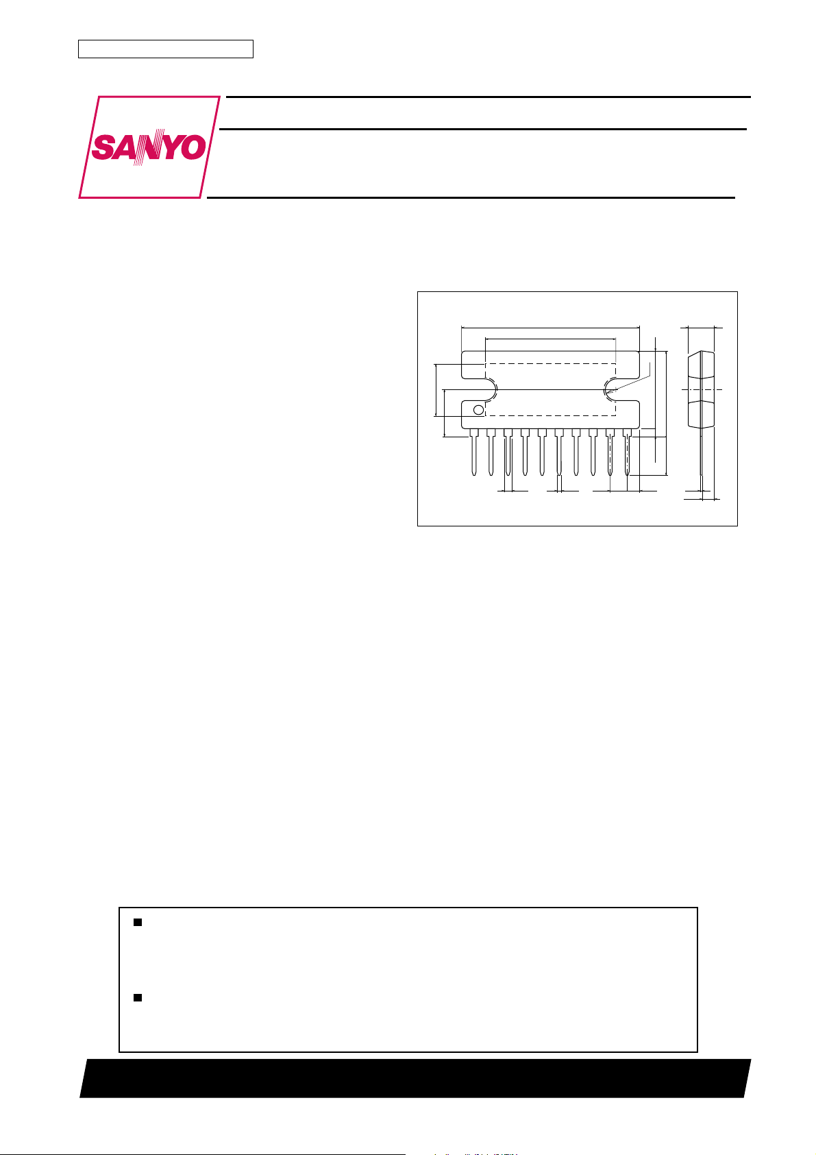
Package Dimensions
unit:mm
3024A-SIP10H
[LA4460N, 4461N]
27.0
20.0
8.4
7.0
1.4
0.5
2.54
101
4.0
R1.7
11.8
13.2max
6.0
1.0min
2.07
SANYO : SIP10H
0.4
2.0
21500TN (KT)/90196RM/D187KI, TS No.2660–1/12
LA4460N, 4461N
Specifications
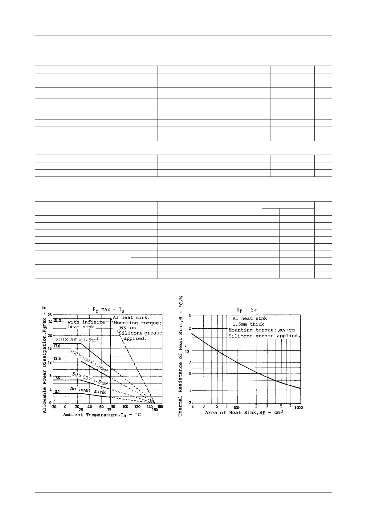
Absolute Maximum Ratings at Ta = 25˚C
retemaraPlobmySsnoitidnoCsgnitaRtinU
egatlovylppusmumixaM
tnerrucylppuSI
tnerructuptuOI
egatlovylppusegruSegrusVt≤ s2.0 05V
noitapissidrewopelbawollAxamdP 52W
ecnatsiserlamrehtegakcaP
erutarepmetgnitarepOrpoT 57+ot02–
erutarepmetegarotSgtsT 051+ot04–
V
V
Recommended Operating Conditions at Ta = 25˚C
retemaraPlobmySsnoitidnoCsgnitaRtinU
egatlovylppusdednemmoceRV
ecnatsiserdaoLR
1xam)s03(tnecseiuQ 52V
CC
2xamlangishtiw 81V
CC
kaep
01
7I,9
θ c-j
CC
L
ylno
kaepytudeulavsuoenatnatsnI ≤ htdiweslup,%5 ≤ sm15.4A
Tc=75˚C, See Pd max – Ta graph.
ytudeulavsuoenatnatsnI ≤ htdiweslup,%5 ≤ ni-wolfsm1
5.4A
3
˚C/W
˚C
˚C
2.31V
Ω
8ot4
Operating Characteristics at Ta = 25˚C, VCC=13.2V, RL=4Ω, f=1kHz, Rg=600Ω, with 100×100×1.5mm
Al heat sink, See specified Test Circuit
retemaraPlobmySsnoitidnoC
tnerructnecseiuQI
niagegatloVGV.tiucricdednemmocerdeificepsta,pooldesolc941535Bd
rewoptuptuOP
noitrotsidcinomrahlatoTDHTPOW1=1.00.1%
ecnatsisertupnIr
egatlovesiontuptuO
egatlovtesffotuptuOffoV003–003+Vm
)CA(noitaunettagnituMA
(Note) : For DC muting, ATT=∞
nimpytxam
OCC
O
i
VON1retlifssap-dnab,zHk02otzH02=f,0=gR4.00.1Vm
VON2k01=gR Ω retlifssap-dnab,zHk02otzH02=f,6.00.2Vm
TT
%01=DHT0121W
V
O
V,mBd0=
V9=83Bd
M
sgnitaR
56021Am
1203kΩ
3
tinU
No.2660–2/12
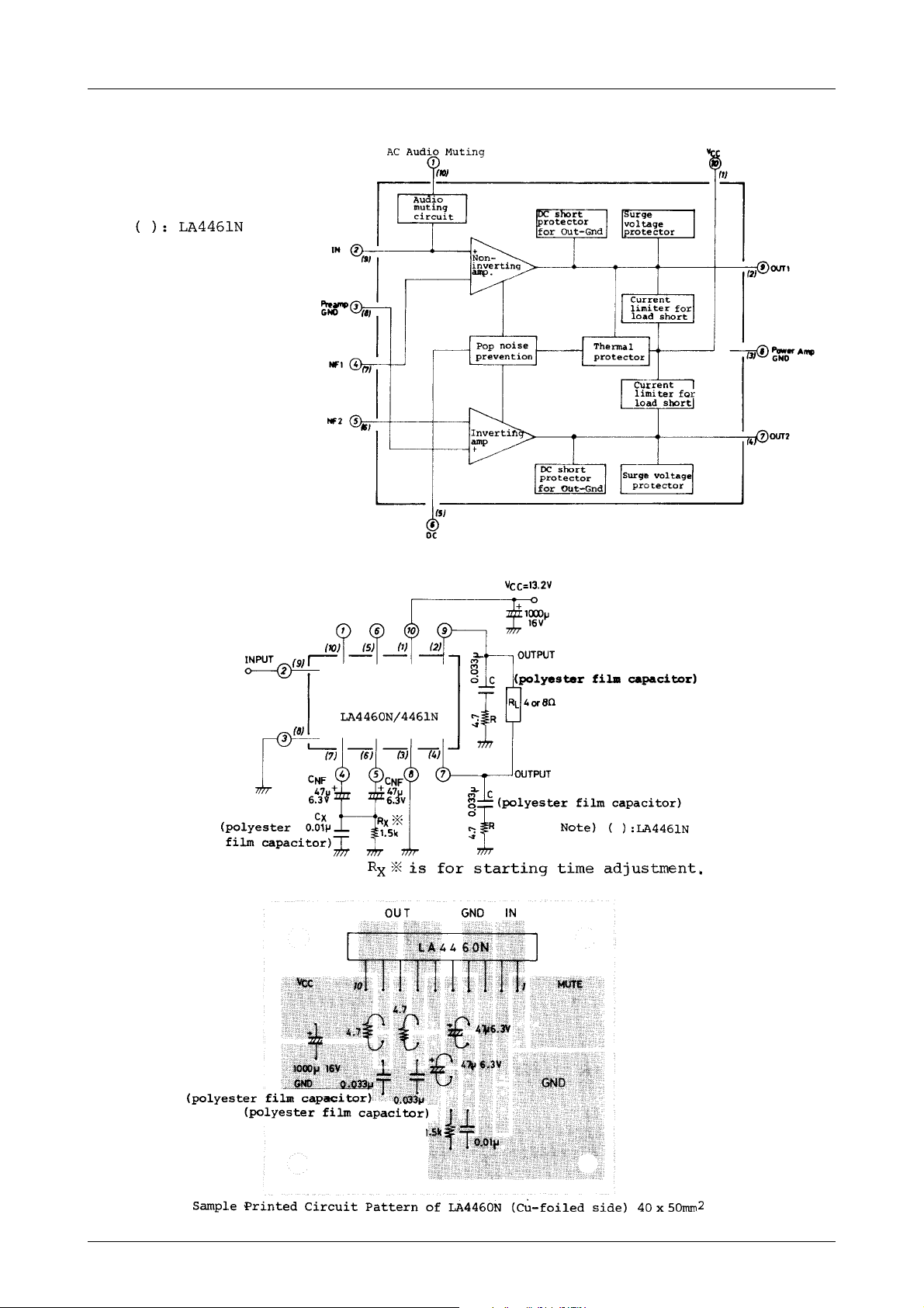
Equivalent Circuit Block Diagram
LA4460N, 4461N
Sample Application Circuit 1 : Recommended Circuit
No.2660–3/12
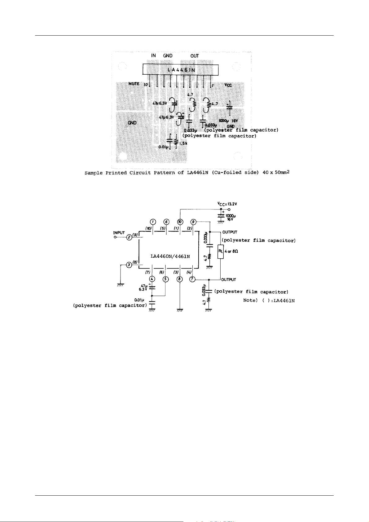
LA4460N, 4461N
Sample Application Circuit 2 : An Example with Minimum Parts
Functional Description on the External Parts
Recommended number of the external parts for the LA4460N/4461N is 8 as shown in the Sample Application Circuit 1.
Namely they are :
· Feedback capacitors 2 pieces 4.7µF/6.3V×2
· Starting time adjustmant resistor 1 pieace 1.5kΩ
· Oscillation compensation capacitor 1 piece 0.01µF
· Oscillation compensation C · R 4 pieces 0.033µF×2, 4.7Ω×2
a) Feedback capacitor CNF
This relates to a low range cutoff frequency fL, and fL lowers with increasing value of the ‘CNF and increases with
decreasing CNF.
b) Oscillation compensation capacitor C
X
Signals are applied from the non-inverted NF ter minal to the inverted NF terminal through the two CNF capacitors. It
is recommended to connect the oscillation compensation capacitor CX=0.01µF between the floating junction of the
capacitors (minus side of CNF) and GND. As a rule a polyester film capacitor is recommended, but a ceramic type
may be used if a PC board shows good circuit stability.
No.2660–4/12
 Loading...