

Philips L6910 Service Manual
ADJUSTABLE STEP DOWN CONTROLLER
WITH SYNCHRONOUS RECTIFICATION
FEATURE
■ OPER ATING SUPPLY VOLTAGE FROM 5V
TO 12V BUSES
■ UP TO 1.3A GATE CURRENT CAPABILITY
■ ADJUSTABLE OUTPUT VOLTAGE
■ N-INVER TING E/A INPUT AVAILABL E
■ 0.9V ±1.5% VOLTAGE REFERENCE
■ VOLTAGE MODE PWM CONTROL
■ VERY FAST LOAD TRANSIENT RESPONSE
■ 0% TO 100% DUTY CYCLE
■ POWER GOOD OUT PUT
■ OVERVOLTAGE PROT EC T ION
■ HICCUP OVERCURRENT PROTECTION
■ 200kHz INTERNAL OSCILLATOR
■ OSCILLATOR EXTERNALLY ADJUSTABLE
FROM 50kHz TO 1MHz
■ SOFT START AND INHIBIT
■ PACKAGES: SO-16 & HTSSOP16
APPLICATIONS
■ SUPPLY FOR MEMORIES AND TERMI-
NATIONS
■ COMPUTER ADD-ON CARDS
■ LOW VOLTAGE DISTRIBUTED DC-DC
■ MAG-AMP RE PL AC EMENT
L6910
L6910A
SO-16 (Narrow) HTSSOP16 (Exposed Pad)
ORDERING NUMBERS:
L6910 (SO-16) L6910A (HTSSOP16)
L6910TR (Tape & Reel) L6910ATR (Tape & Reel)
DESCRIPTION
The device is a pwm controller for high performance
dc-dc conversion from 3.3V, 5V and 12V buses.
The output voltage is adjustable down to 0.9V; higher
voltages can be obtained with an external voltage divider.
High peak current gate drivers provide for fast switching to the external power section, and the output
current can be in excess of 20A.
The device assures protections agains t load overcurrent and overvoltage. A n internal c rowbar i s als o provided turning on the low side mosfet as long as the
over-voltage is detected. In case of over-current detection, the soft start capacitor is discharged and the
system works in HICCUP mode.
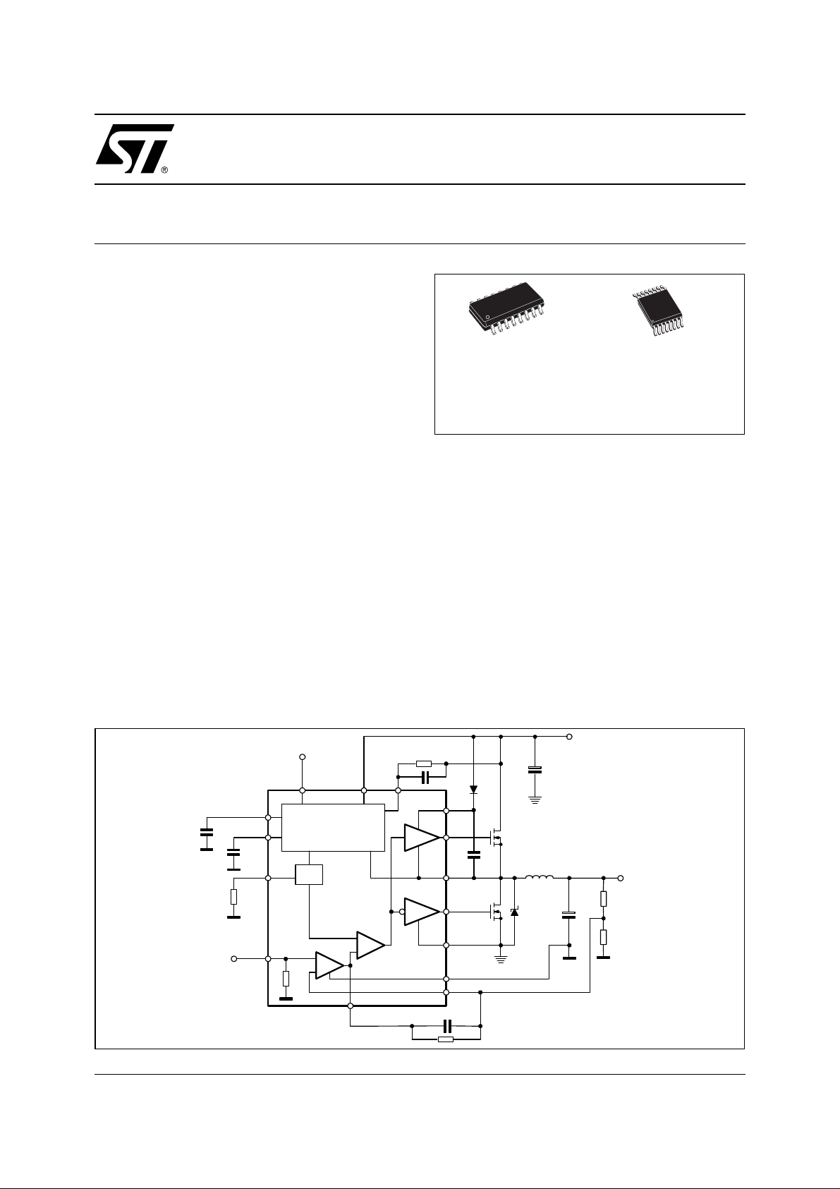
BLOCK DIAGRAM
October 2003
Vin 5V to12V
PGOOD
VCC OCSET
VREF
SS
OSC
RT
EAREF
Monitor
Protec tion and R ef
OSC
L6910
-
+
E/A
+
-
300k
COMP
PWM
BOOT
UGATE
PHASE
LGATE
PGND
GND
VFB
Vo
1/25
L6910A L6910
ABSOLUTE MAXIMUM RATINGS
Symbol Parameter Value Unit
Vcc Vcc to GND, PGND 15 V
V
-
BOOT
V
PHASE
V
HGATE
V
PHASE
Boot Voltage 15 V
-
OCSET, LGATE, PHASE -0.3 to Vcc+0.3 V
SS, FB, PGOOD, VREF, EAREF, RT 7 V
COMP 6.5 V
15 V
T
T
stg
P
tot
Junction Temperature Range -40 to 150 °C
j
Storage temperature range -40 to 150 °C
Maximum power dissipation at Tamb = 25°C1W
THERMAL DATA
Symbol Parameter SO-16 HTSSOP16 HTSSOP16 (*) Unit
R
th j-amb
(*) Device soldered on 1 S2P PC board
PINS CONNECTION
OCSET
SS/INH
EAREF PGOOD
Thermal Resistance Junction to Ambient 120 110 50 °C/W
(Top view)
VREF
OSC
COMP
FB
GND
16
2
3
4
5
6
7
8
15
14
13
12
11
10
9
SO16
N.C.1
VCC
LGATE
PGND
BOOT
HGATE
PHASE
VREF
OSC
OCSET
SS/INH
N.C.
COMP
FB
GND EAREF
1
2
3
4
5
6
7
8
HTSSOP-16
16
15
14
13
12
11
10
9
VCC
LGATE
PGND
BOOT
HGATE
PHASE
PGOOD
2/25

L6910A L6910
PINS FUNCTION
SO HTSSOP Name Description
1 1 VREF Inter nal 0.9V ±1.5% reference is available for external regulato rs or for the internal error
2 2 OSC Oscillator switching frequency p in. Connecting an external resistor ( R
3 3 OCSET A resistor connected from this pin and the upper Mos Drain sets the current limit
4 4 SS/INH The soft star t time is programmed connec ting an external capacitor from this pin and
5 6 COMP This pin is con necte d to the err or amplifie r ou tput and is used to comp ensa te th e voltag e
6 7 FB This pin is co nnec ted to t he error amplifier inver ting inpu t an d is us ed to c ompe nsate th e
7 8 GND All the internal references are referred to this pin. Connect it to the PCB signal ground.
8 9 EAREF Error amplifier non-inverting inpu t. Conn ect to this pin an exter nal reference (from 0.9V to
910
PGOOD
10 11 PHASE
11 12 HGATE High side gate driver output.
12 13 BOOT Bo otstrap capacitor pin. Thro ugh this pin is supplied the high side driver and the uppe r
13 14 PGND Power ground pin. This pin h as to be connected closely to the low side mosfet source i n
14 ‘5 LGATE This pin is the lower mosfet gate driver output
15 16 VCC Device supply voltage. The operative supply voltage ranges is from 5V to 12V.
16 5 N.C. This pin is not internally bonded. It may be left floating or connected to GND.
amplifier (connecting this pin to EAREF) if external reference is not available.
A minimum 1nF capacitor is required.
If the pin is forced to a voltage lower than 70%, the device enters the hiccup mode.
) from this p in to
T
GND, the external frequency is increased according to the equation:
f
OSC,RT
200KHz
4.94 10
-------------------------+=
RTKΩ()
6
⋅
Connecting a resistor (RT) from thi s pin to Vcc (12V) , the switc hing frequency is reduced
accordi ng to the equation:
f
OSC,RT
200KHz
4.306 107⋅
---------------------------- -–=
RTKΩ()
If the pin is not connected, the switching frequency is 200KHz.
The voltage at this p in is fixed at 1.23V. Forcing a 50µA curren t into this pin, the built i n
oscillator stops to switch.
In Over Voltage condition this pin goes over 3V until that conditon is removed.
protection.
The internal 200µA current generator sinks a constant current through the external
resistor. The Over-Current threshold is due to the following equation:
I
I
--------------------------------------------- -=
P
⋅
OCSETROCSET
R
DSon
GND. The internal current generator forces through the capacitor 10µA.
This pin can be used to disable the device forcing a voltage lower than 0.4V
control feedback loop.
voltage control feedback loop.
Connected to t he out put res istor d ivider, if used, or di rectly to Vout, it manages also overvoltage conditions and the PGOOD signal
3V) for the PWM regulation or short it to VREF pin to use the internal reference.
If this pin goes under 650mV (typ), the device shuts down.
This pin is an open collector output and it is pulled low if the output voltage is not within the
above specified thresholds. If not used it may be left floating.
This pin is conne cted to the sour ce of the upper mosfet and provi des the ret urn path for the
high side driver. This pin monitors the drop across the upper mosfet for the current limit
together with OCSET.
mosfet. Connect through a capacitor to the PHASE pin and through a diode to Vcc
(cathode vs. boot).
order to reduce the noise injection into the device
DO NOT CONNECT V
TO A VOLTAGE GREATER THAN VCC.
IN
3/25
L6910A L6910
ELECTRICAL CHARACTERISTICS
(Vcc = 12V, TJ =25°C unless otherwise specified)
Symbol Parameter Test Condition Min Typ Max Unit
V
SUPPLY CURRENT
cc
Icc Vcc Supply current OSC = open; SS to GND 4 7 9 mA
POWER-ON
Turn-On Vcc threshold VOCSET = 4V 4.0 4.3 4.6 V
Turn-Off Vcc threshold VOCSET = 4V 3.8 4.1 4.4 V
Rising V
threshold 1.24 1.4 V
OCSET
Turn On EAREF threshold VOCSET = 4V 650 750 mV
SOFT START AND INHIBIT
Iss Soft start Current
S.S. current in INH condition
SS = 2V
SS = 0 to 0.4V
6103514
60
OSCILLATOR
f
OSC
f
OSC,RT
Initial Accuracy OSC = OPEN
OSC = OPEN; T
= 0° to 125°
j
180
170
Total Accuracy 16 KΩ < RT to GND < 200 KΩ -15 15 %
200 220
230
∆Vosc Ramp amplitude 1.9 V
REFERENCE
V
V
V
Output Voltage Accuracy V
OUT
Reference Voltage C
REF
Reference Voltage C
REF
= VFB; V
OUT
= 1nF; I
REF
= 1nF; TJ = 0 to 125°C-2 +2%
REF
= V
EAREF
REF
REF
= 0 to 100µA 0.886 0.900 0.913 V
0.886 0.900 0.913 V
ERROR AMPLIFIER
I
EAREF
N.I. bias current V
= 3V 10 µA
EAREF
EAREF Input Resistance Vs. GND 300 kΩ
I.I. bias current VFB = 0V to 3V 0.01 0.5 µA
FB
Common Mode Voltage 0.8 3 V
CM
Output Voltage 0.5 4 V
Open Loop Voltage Gain 70 85 dB
V
V
V
COMP
I
G
GBWP Gain-Bandw idth Produ ct 10 MHz
SR Slew-Rate COMP = 10pF 10 V/µs
GATE DRIVERS
I
HGATE
R
HGATE
High Side
Source Current
High Side
V
BOOT
V
HGATE
V
BOOT
- V
- V
- V
= 12V
PHASE
= 6V
PHASE
= 12V 2 4 Ω
PHASE
1 1.3 A
Sink Resistance
I
LGATE
R
LGATE
Low Side Source Current Vcc = 12V; V
Low Side Sink Resistance Vcc = 12V 1.5 3 Ω
= 6V 0.9 1.1 A
LGATE
Output Driver Dead Time PHASE connected to GND 90 210 ns
PROTECTIONS
I
OCSET
I
OSC
OCSET Current Source V
Over Voltage Trip (V
FB
/ V
)VFB Rising 117 120 %
EAREF
OSC Sourcing Current V
= 4V 170 200 230 µA
OCSET
> OVP Trip 15 30 mA
FB
POWER GOOD
V
PGOOD
I
PGOOD
Upper Threshold (V
Lower Threshold (V
Hysteresis (V
FB
PGOOD Voltage Low I
Output Leakage Current V
/ V
/ V
FB
/ V
FB
EAREF
)VFB Rising 108 110 112 %
EAREF
)VFB Falling 88 90 92 %
EAREF
) Upper and Lower threshold 2 %
= -4mA 0.4 V
PGOOD
= 6V 0.2 1 µA
PGOOD
µA
µA
KHz
kHz
4/25
L6910A L6910
Device Description
The device is an integrated circuit realized in BCD technology. The controller provides complete control logic and
protection for a high performance step-down DC-DC converter. It is designed to drive N Channel Mosfets in a
synchronous-rectified buck topology. The output voltage of the converter can be precisely regulated down to
900mV with a maximum tolerance of ±1.5% when the internal reference is used (simply connecting together
EAREF and VREF pins). The device allows also using an external reference (0.9V to 3V) for the regulation. The
device provides voltage-mode control with fast transient response. It includes a 200kHz free-running oscillator that
is adjustable from 50kHz to 1MHz. The error amplifier features a 10MHz gain-bandwidth product and 10V/
rate that permits to realize high converter bandwidth for fast transient performance. The PWM duty cycle can
range from 0% to 100%. The device protects against over-current conditions entering in HICCUP mode. The device monitors the current by using the r
of the upper MOSFET(s) that eliminates the need for a current
DS(ON)
sensing resi stor. The device is available in SO16 narrow package.
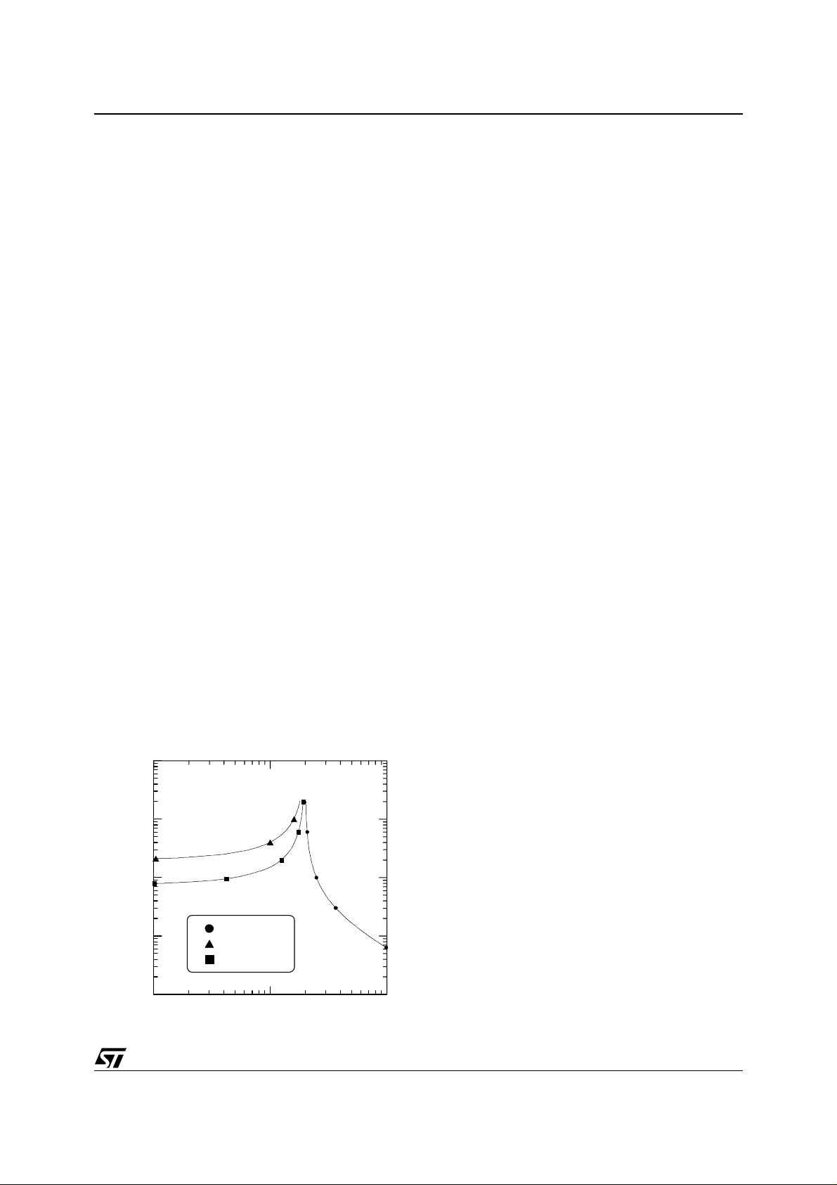
Oscillator
The switching frequency is internally fixed to 200kHz. The internal oscillator generates the triangular waveform
for the PWM charging and discharging with a constant c urrent an internal capacit or. The current delivered to the
oscillator is typicall y 50
OSC pin and GND or V
µ
A (Fsw = 200KHz) and may be varied using an external resistor (RT) connected between
. Since the OSC pin is maintained at fixed voltage ( typ. 1.235V) , the frequency is var-
CC
ied proportionally to the current sunk (forced) from (into) the pin.
In particular connecting R
vs. GND the frequency is increased (current is sunk from the pin), according to the
T
following relationship:
6
⋅
4.94 10
-------------------------+=
R
KΩ()
T
Connecting R
f
OSC,RT
to VCC = 12V or to VCC = 5V the frequency is reduced (current is forced into the pin), according
T
200KHz
to the following relationships:
7
⋅
f
OSC,RT
200KHz
4.306 10
---------------------------- -–=
R
T
KΩ()
V
CC
= 12V
µ
s slew
f
OSC,RT
200KHz
15 10
---------------------–=
R
T
Switching frequency variation vs. RT are repeated in Fig. 1.
Note that forcing a 50
µ
A current into this pin, the device stops switching because no current is delivered to the
oscillator.
Figure 1.
10000
Reference
A precise ±1.5% 0.9V reference is a vailable. This reference must be fi ltered w ith 1nF ceramic capaci tor to
avoid instability in the internal linear regulator. It is
able to deliver up to 100
1000
erence for the device regulation and also for other devices. If forced under 70% of its nominal value, the
device enters in Hiccup mode until this condition is
100
removed.
Through the EAREF pin the reference for the regula-
tion is taken. This pin directly connects the non-in-
Resistance [kOhm]
10
RT to GND
RT to VCC=12V
RT to VCC=5V
verting input of the error amplifier. An external
reference (or the internal 0.9V ±1.5%) may be used.
The input for this pin can range from 0.9V to 3V. It
has an internal pull-down (300k
the device shutdown if no reference is connected ( pin
10 100 1000
Frequency [kHz]
floating). However the device is shut down if the voltage on the EAREF pin is lower than 650mV (typ).
6
⋅
KΩ()
V
= 5V
CC
µ
A and may be used as ref-
Ω
resistor) that forces
5/25
L6910A L6910
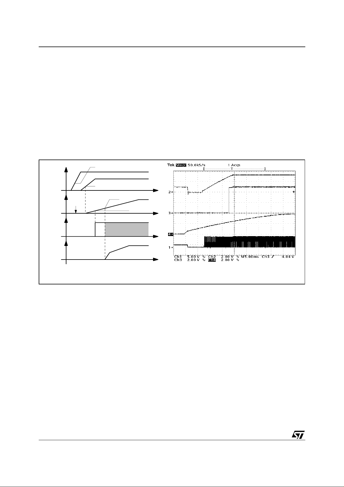
Soft Start
At start-up a ramp is generated charging the external capacitor CSS with an internal current generator. The initial
value for this current is of 35
10
µ
A until the final charge value of approximatively 4V.
When the voltage across the soft start capacitor (V
charge the output capacitor. As V
MOS begins to switch and the output voltage starts to increase.
No switching activity is observable if SS is kept lower than 0.5V and both mosfets are off.
If VCC and OCSET pins are not above their own turn-on thresholds and V
Start will not take place, an d the r elati ve pin is i nternally shorted to G ND. Duri ng nor mal ope ration, if any undervoltage is detected on one of the two supplies, the SS pin is internally shorted to GND and so the SS capacitor
is rapidly discharged.
Figure 2. Soft Start (with Reference Present)
µ
A and speeds-up the charge of the capacitor up to 0.5V. After that it becames
) reaches 0.5V the lower power MOS is turned on to dis-
reaches 1.1V ( i.e. th e osc illator triangular wave inferi or lim it) als o the upper
SS
SS
is not above 650mV, the Soft-
EAREF
Vcc
Vin
Vss
LGATE
Vout
to GND
Vcc Turn-on threshold
Vin Turn-on th reshold
1V
Timing Diagram
0.5V
Acquisition: CH1 = PHASE; CH2 = V
CH3 = PGOOD; CH4 = V
ss
out
;
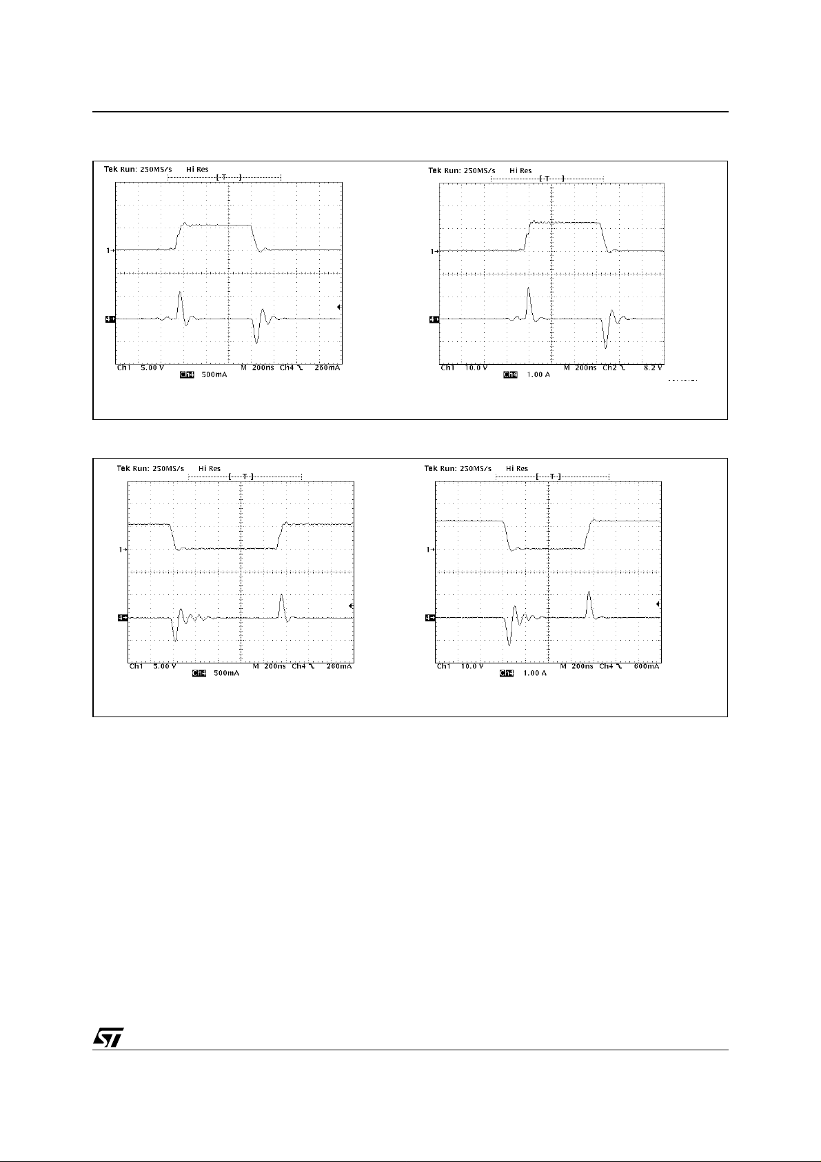
Driver Section
The driver capability on the high and low side drivers allows using different types of power MOS (also multiple
MOS to reduce the R
), maintaining fast switching transition.
DSON
The low-side mos driver is supplied directly by Vcc while the high-side driver is supplied by the BOOT pin.
Adaptative dead time control i s implemented to pr event cross-c onduction and allow to use several kinds o f mos-
fets. The upper mos turn-on is avoided if the lower gate is over about 200mV while the lower mos turn-on is
avoided if the PHASE pin is over about 500mV. The lower mos is in any case turned-on after 200ns from the
high side turn-off.
The peak current is shown for both the upper ( fig. 3) and the low er (fig. 4) driv er at 5V and 12V. A 3.3nF capacitive load has been used in these measurements.
For the lower driver, the source peak current is 1.1A @ V
current is 1.3A @ V
= 12V and 500mA @ VCC = 5V.
CC
= 12V and 500mA @ VCC = 5V, and the sink peak
CC
Similarly, for the upper driver, the source peak current is 1.3A @ Vboot-Vphase = 12V and 600mA @ VbootVphase = 5V, and the sink peak current is 1.3A @ Vboot-Vphase =12V and 550mA @ Vboot-Vphase = 5V.
6/25
L6910A L6910
Figure 3. High Side driver peak current. Vboot-Vphase = 12V (right) Vboot-Vphase = 5V (left)
CH1 = High Side Gate CH4 = Gate Current
Figure 4. Low Side driver peak curren t. VCC = 12V (right) VCC = 5V (left)
CH1 = Low Side Gate CH4 = Gate Current
Monitoring and Protections
The output voltage is monitored by means of pin FB. If it is not wi thin ±10% (typ.) of the programmed v alue, the
powergood output is forced low.
The device provides overvoltage protection, when the voltage sensed on pin FB reaches a value 17% (typ.)
greater than the reference the OSC pin is forced high (3V typ.) and the lower driver is turned on as long as the
over-voltage is detected.
Overcurrent protection is performed by the device comparing the drop across the high side MOS, due to the
R
, with the voltage across the exte rnal resistor (R
DSON
upper MOS. Thus the overcurrent threshold (I
Where the typical value of I
R
(also the variation with temperature) and the minimum value of I
dsON
is 200µA. To calculate the R
OCS
) can be calculated with the following relationship:
P
I
P
) connected between the OCSET pin and drain of the
OCS
R
⋅
OCSIOCS
-------------------------------- -=
R
dsON
value it must be considered the maximum
OCS
. To avoid undesirable trigger of
OCS
overcurrent protection this relationship must be satisfied:
7/25
L6910A L6910
µH,
µH,
I∆
IPI
OUTMAX
Where ∆I is the inductance ripple current and I
OUTMAX
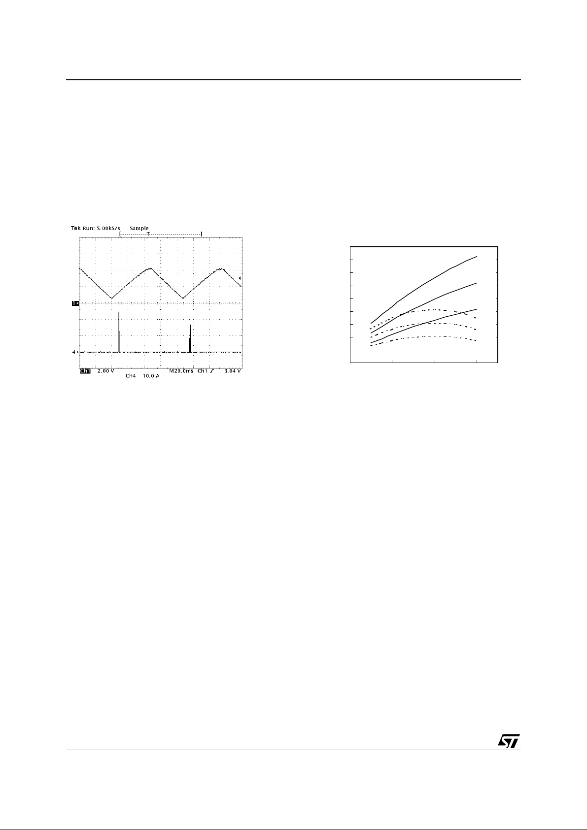
In case of ov er current de tectionthe soft s tart capacitor is discharged w ith constant current (10
the SS pin reaches 0.5V the soft start phase is restarted. During the soft start the over-current protection is always active and if such kind of event occurs, the device turns off both mosfets, and the SS capacitor is discharged again (after reaching the upper threshold of about 4V). The system is now working in HICCUP mode,
as shown in figure 5. After removing the cause of the over-current, the device restart working normally without
power supplies turn off and on.
Figure 5. Hiccup Mode Figure 6. Indu ct or ri pp le current vs. Vout
---- -+≥ I
=
PEAK
2
is the maximum output current.
µ
A typ.) and when
CH1 = SS; CH4 = Inductor current
9
8
7
6
5
4
3
2
Inductor Ripple [A]
1
0
0.51.52.53.5
Output Voltage [V]
L=1.5
Vin=12V
L=3
Vin=5V
L=2µH,
Vin=12V
L=3µH,
Vin=12V
L=1.5µH,
Vin=5V
L=2µH,
Vin=5V
Inductor design
The inductance value is defined by a compromise between the transient response time, the efficiency, the cost
and the size. The inductor has to be calculated to sustain the output and the input voltage variation to maintain
the ripple current
∆
IL between 20% and 30% of the maximum output current. The inductance value can be cal-
culated with this relationship:
–
V
INVOUT
----------------------------- -
Where f
L
is the switching frequency, VIN is the input voltage and V
SW
f
swIL
the ripple current vs. the output voltage for different values of the inductor, with V
V
OUT
-------------- -
⋅=
∆⋅
V
IN
is the output voltage. Figure 6 shows
OUT
= 5V and VIN = 12V.
IN
Increasing the value of the inductance reduces the ripple current but, at the same time, reduces the converter
response time to a load transient. If the compensation network is well designed, the device is able to open or
close the duty cycle up to 100% or down to 0%. The response time is now the time required by the inductor to
change its current from initial to final val ue. S ince the ind uctor has not fini shed its charging tim e, the output cur rent is supplied by the output capacitors. Minimizing the response time can minimize the output capacitance
required.
The response time to a load transient is different for the application or the removal of the load: if during the application of the lo ad the inductor is c harged by a voltage equal to the differ ence between the input and th e output
voltage, during the removal it is discharged only by the output voltage. The following expressions give approximate response time for
∆
I load transient in case of enough fast compensation network response:
t
applicatio n
LI∆⋅
----------------------------- –
V
INVOUT
t
removal
LI∆⋅
-------------- -==
V
OUT
The worst condition depends on the input voltage available and the output voltage selected. Anyway the worst
case is the response ti me after removal o f the load with the mi nimum output v oltage progr ammed and the maximum input voltage available.
8/25
 Loading...