

Philips KMZ10A1 Datasheet
DISCRETE SEMICONDUCTORS
DATA SH EET
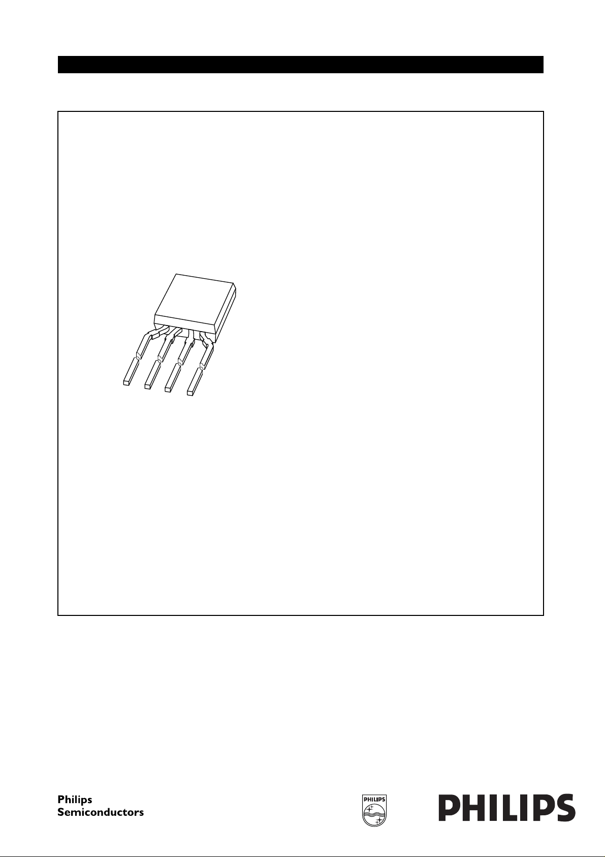
handbook, halfpage
M3D329
KMZ10A1
Magnetic field sensor
Product specification
Supersedes data of 1996 Nov 14
File under Discrete Semiconductors, SC17
1998 Apr 06
Philips Semiconductors Product specification
Magnetic field sensor KMZ10A1
DESCRIPTION
The KMZ10A1 is an extremely sensitive magnetic field
sensor, employing the magnetoresistive effect of thin-film
permalloy. Its properties enable this sensor to be used in a
wide range of applications such as navigation, current and
earth magnetic field measurement etc. The special
arrangement of the sensing chip allows the construction of
coils for switching the auxiliary field (Hx) along the length
axis of the sensor. The sensor can be operated at any
frequency between DC and 1 MHz.
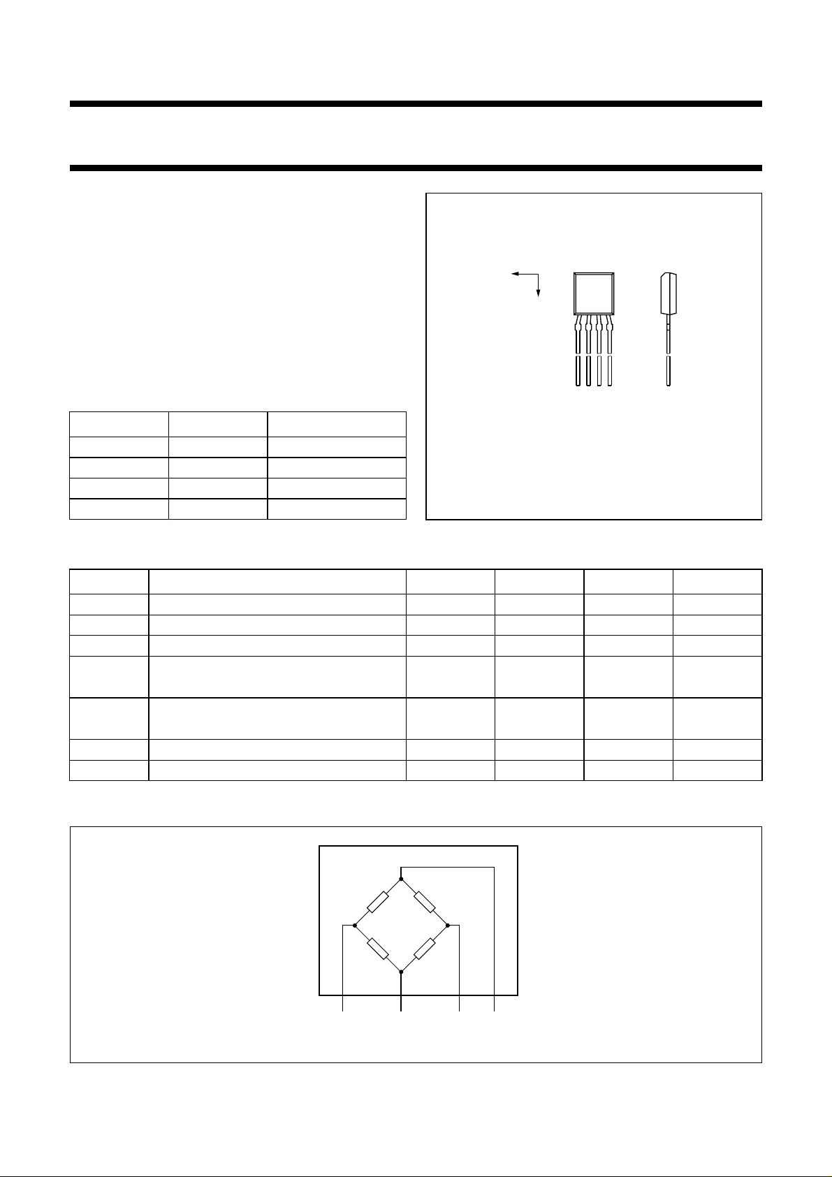
H
handbook, halfpage
y
H
x
PINNING
1234
MGL420
PIN SYMBOL DESCRIPTION
1+V
O
output voltage
2 GND ground
3 −V
4V
O
CC
output voltage
supply voltage
Fig.1 Simplified outline.
QUICK REFERENCE DATA
SYMBOL PARAMETER MIN. TYP. MAX. UNIT
V
CC
H
y
H
x
S sensitivity − 14 −
S
s
R
bridge
V
offset
DC supply voltage − 5 − V
magnetic field strength −0.5 − +0.5 kA/m
auxiliary field − 0.5 − kA/m
mV V⁄
----------------kA m⁄
sensitivity (with switched Hx) − 22 −
mV V⁄
----------------kA m⁄
bridge resistance 0.85 − 1.75 kΩ
offset voltage −1.5 − +1.5 mV/V
CIRCUIT DIAGRAM
handbook, full pagewidth
1
+V
O
GND
Fig.2 Simplified circuit diagram.
1998 Apr 06 2
–V
MLC716
432
V
O
CC
Philips Semiconductors Product specification
Magnetic field sensor KMZ10A1
LIMITING VALUES
In accordance with the Absolute Maximum Rating System (IEC 134).
SYMBOL PARAMETER CONDITIONS MIN. MAX. UNIT
V
CC
P
tot
T
stg
T
bridge
DC supply voltage − 9V
total power dissipation up to T
= 132 °C − 100 mW
amb
storage temperature −65 +150 °C
bridge operating temperature −40 +150 °C
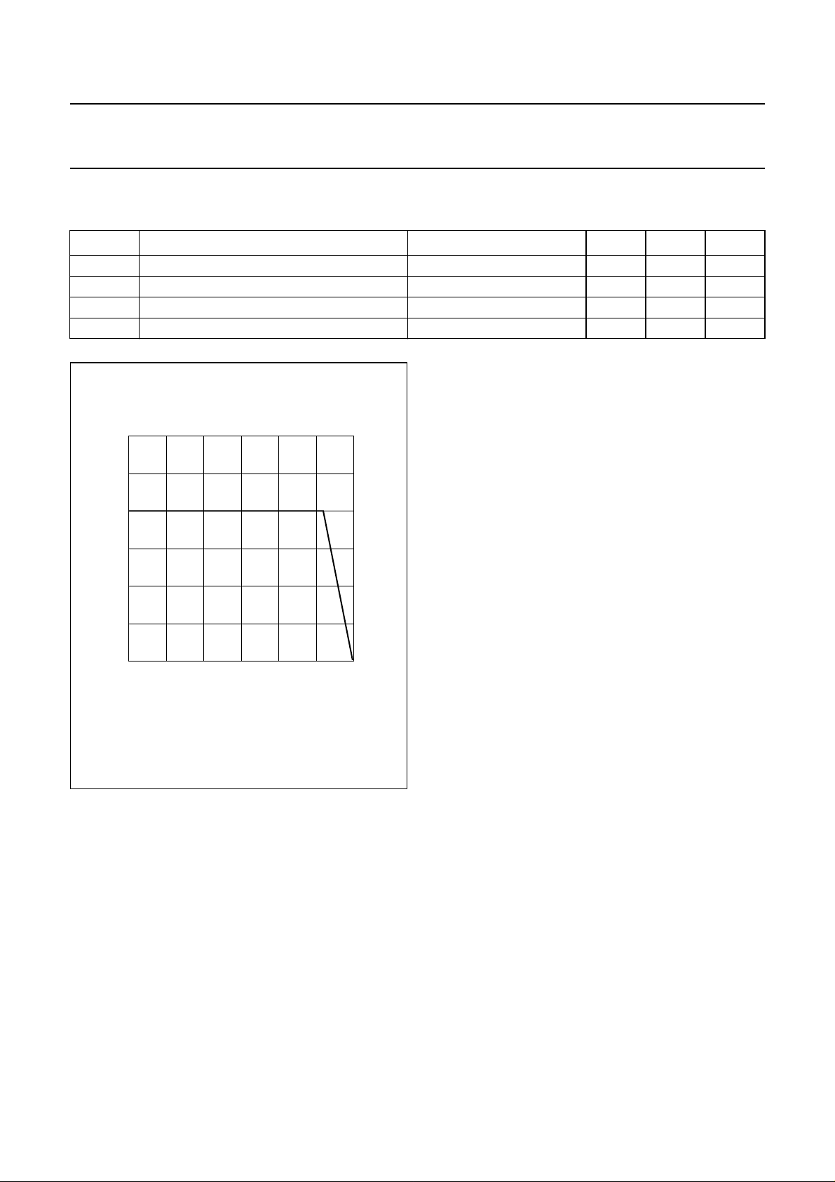
150
handbook, halfpage
P
tot
(mW)
100
50
0
0
50 100 150
T ( C)
amb
Fig.3 Power derating curve.
MSA927
o
1998 Apr 06 3

Philips Semiconductors Product specification
Magnetic field sensor KMZ10A1
THERMAL CHARACTERISTICS
SYMBOL PARAMETER VALUE UNIT
R
th j-a
CHARACTERISTICS
=25°C and Hx= 0.5 kA/m unless otherwise specified; see notes 1 and 2.
T
amb
SYMBOL PARAMETER CONDITIONS MIN. TYP. MAX. UNIT
V
CC
H
y
S sensitivity open circuit;
TCV
O
VCV
O
R
bridge
TCR
bridge
V
offset
TCV
offset
FL linearity deviation of output voltage H
FH hysteresis of output voltage −−0.5 %⋅FS
f operating frequency 0 − 1 MHz
thermal resistance from junction to ambient 180 K/W
DC supply voltage − 5 − V
operating range note 2 −0.5 −+0.5 kA/m
temperature coefficient of output
voltage at constant supply voltage
temperature coefficient of output
voltage at constant supply current
notes 2 and 3
VCC=5V;
T
= −25 to +125 °C
amb
IB= 3 mA;
T
= −25 to +125 °C
amb
11 − 17
−−0.4 − %/K
−−0.15 − %/K
mV V⁄
----------------kA m⁄
bridge resistance 0.85 − 1.75 kΩ
temperature coefficient of bridge
Tj= −25 to +125 °C − 0.25 − %/K
resistance
offset voltage −1.5 − +1.5 mV/V
offset voltage drift T
= −25 to +125 °C −6 −+6
bridge
=0to±0.25 kA/m
y
=0to±0.4 kA/m
H
y
H
=0to±0.5 kA/m
y
−1
−−0.8 %⋅FS
−1
−1
−−2.5 %⋅FS
−−4.0 %⋅FS
µ VV⁄
---------------
K
Characteristics with H
H
S
y
s
operating range note 2 −0.05 −+0.05 kA/m
sensitivity slope between Hy=0
= 0 (switched Hx, see note 4); VCC=5V
x
and Hy= 40 A/m
14 − 27
mV V⁄
----------------kA m⁄
Notes
1. Before first operation or after operation outside the SOAR (Fig.4) the sensor has to be reset by application of an
auxiliary field H
2. No disturbing field (H
= 3 kA/m.
x
) allowed; for stable operation under disturbing conditions see Fig.4 (SOAR) and see Fig.5 for
d
decrease of sensitivity.
3. Sensitivity measured as ∆V
/∆Hy between Hy= 0 and Hy= 0.4 kA/m.
O
4. See application information.
1998 Apr 06 4
 Loading...