

Philips icm7555, icm7555i, icm7555c DATASHEETS

Philips Semiconductors Linear Products Product specification
ICM7555General purpose CMOS timer
337
August 31, 1994 853-1192 13721
DESCRIPTION
The ICM7555 is a CMOS timer providing significantly improved
performance over the standard NE/SE555 timer, while at the same
time being a direct replacement for those devices in most
applications. Improved parameters include low supply current, wide
operating supply voltage range, low THRESHOLD, TRIGGER
, and
RESET
currents, no crowbarring of the supply current during output
transitions, higher frequency performance and no requirement to
decouple CONTROL VOLTAGE for stable operation.
The ICM7555 is a stable controller capable of producing accurate
time delays or frequencies.
In the one-shot mode, the pulse width of each circuit is precisely
controlled by one external resistor and capacitor. For astable
operation as an oscillator, the free-running frequency and the duty
cycle are both accurately controlled by two external resistors and
one capacitor. Unlike the bipolar 555 device, the CONTROL
VOLTAGE terminal need not be decoupled with a capacitor. The
TRIGGER
and RESET inputs are active low. The output inverter can
source or sink currents large enough to drive TTL loads or provide
minimal offsets to drive CMOS loads.
FEATURES
•Exact equivalent in most applications for NE/SE555
•Low supply current: 80µA (typ)
•Extremely low trigger, threshold, and reset currents: 20pA (typ)
•High-speed operation: 500kHz guaranteed
•Wide operating supply voltage range guaranteed 3 to 16V over full
automotive temperatures
•Normal reset function; no crowbarring of supply during output
transition
•Can be used with higher-impedance timing elements than the
bipolar 555 for longer time constants
PIN CONFIGURATION
THRESHOLD
D and N Packages
DISCHARGE
V
DD
CONTROL VOLTAGE
1
2
3
4 5
6
7
8
GND
TRIGGER
OUTPUT
RESET
•Timing from microseconds through hours
•Operates in both astable and monostable modes
•Adjustable duty cycle
•High output source/sink driver can drive TTL/CMOS
•Typical temperature stability of 0.005%/
o
C at 25°C
•Rail-to-rail outputs
APPLICATIONS
•Precision timing
•Pulse generation
•Sequential timing
•Time delay generation
•Pulse width modulation
•Pulse position modulation
•Missing pulse detector
ORDERING INFORMATION
DESCRIPTION TEMPERATURE RANGE ORDER CODE DWG #
8-Pin Plastic Dual In-Line Package (DIP) 0 to +70°C ICM7555CN 0404B
8-Pin Plastic Small Outline (SO) Package 0 to +70°C ICM7555CD 0174C
8-Pin Plastic Dual In-Line Package (DIP) -40 to +85°C ICM7555IN 0404B
8-Pin Plastic Small Outline (SO) Package -40 to +85°C ICM7555ID 0174C
Philips Semiconductors Linear Products Product specification
ICM7555General purpose CMOS timer
August 31, 1994
338
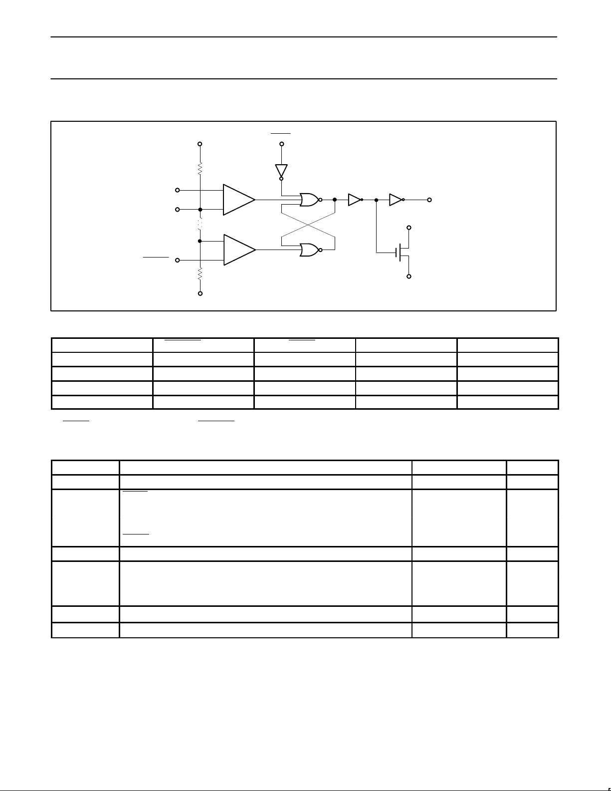
EQUIVALENT BLOCK DIAGRAM
NOTE:
UNUSED INPUTS SHOULD BE CONNECTED TO APPROPRIATE VOLTAGE FROM TRUTH TABLE.
V
DD
8
R
6
5
2
R
1
R
COMPARATOR
A
COMPARATOR
B
FLIP–FLOP
RESET
4
OUTPUT
DRIVERS
3
OUTPUT
DISCHARGE
7
N
1
+
–
+
–
THRESHOLD
CONTROL
VOLTAGE
TRIGGER
TRUTH TABLE
THRESHOLD VOLTAGE TRIGGER VOLTAGE RESET
1
OUTPUT DISCHARGE SWITCH
DON’T CARE DON’T CARE LOW LOW ON
>2/3(V+) > 1/3(V+) HIGH LOW ON
VTH < 2/3 VTR > 1/3 HIGH STABLE STABLE
DON’T CARE <1/3(V+) HIGH HIGH OFF
NOTES:
1. RESET will dominate all other inputs: TRIGGER will dominate over THRESHOLD.
ABSOLUTE MAXIMUM RATINGS
1
SYMBOL
PARAMETER RATING UNITS
V
DD
Supply voltage +18 V
V
TRIG
1
Trigger input voltage
V
CV
Control voltage > -0.3 to
V
TH
Threshold input voltage <VDD + 0.3 V
V
RST
RESET input voltage
I
OUT
Output current 100 mA
P
DMAX
Maximum power dissipation, TA = 25°C (still air)
2
N package 1160 mW
D package 780 mW
T
STG
Storage temperature range -65 to +150
°C
T
SOLD
Lead temperature (Soldering 60s) 300
°C
NOTES:
1. Due to the SCR structure inherent in the CMOS process used to fabricate these devices, connecting any terminal to a voltage greater than
V
DD
+ 0.3V or less than GND -0.3V may cause destructive latch-up. For this reason it is recommended that no inputs from external sources
not operating from the same power supply be applied to the device before its power supply is established. In multiple systems, the supply of
the ICM7555 must be turned on first.
2. Derate above 25°C, at the following rates:
N package at 9.3mW/°C
D package at 6.2mW/°C
3. See “Power Dissipation Considerations” section.
Philips Semiconductors Linear Products Product specification
ICM7555General purpose CMOS timer
August 31, 1994
339
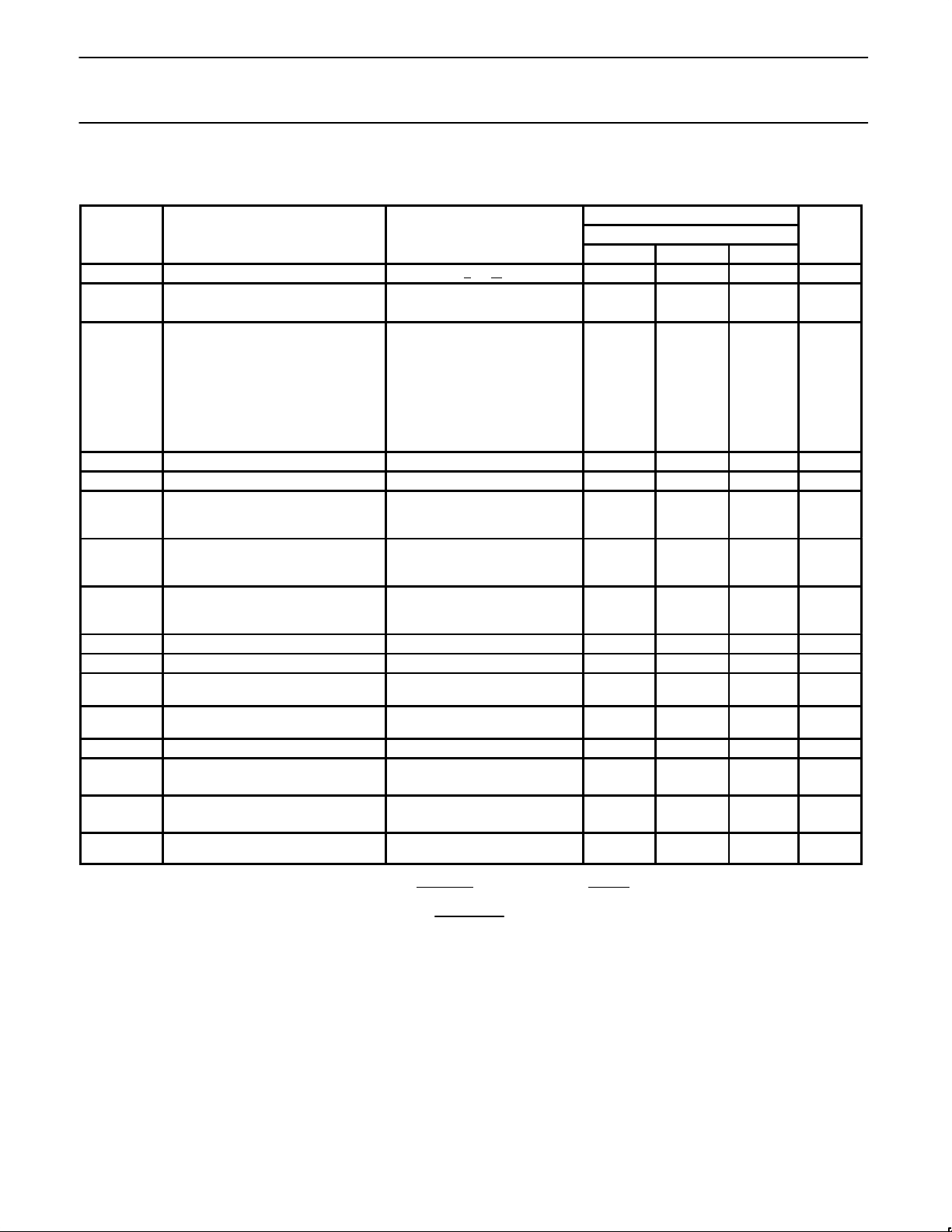
DC AND AC ELECTRICAL CHARACTERISTICS
TA = 25°C unless otherwise specified.
LIMITS
SYMBOL
PARAMETER
TEST CONDITIONS
ICM7555
UNITS
MIN TYP MAX
V
DD
Supply voltage T
MIN
< TA < T
MAX
3 16 V
I
DD
Supply current
1 V
DD
= V
MIN
VDD = V
MAX
50
180
200
300
µA
µA
Astable mode timing
2
Initial accuracy
Drift with supply voltage
Drift with temperature
3
RA, RB = 1k to 100k, C = 0.1µF
5V <V
DD
<15V
V
DD
= 5V
V
DD
= 10V
V
DD
= 15V
1.0
0.1
50
75
100
5.0
3.0
%
%/V
ppm/
o
C
ppm/
o
C
ppm/
o
C
V
TH
Threshold voltage VDD = 5V 0.63 0.65 0.67 xV
DD
V
TRIG
Trigger voltage VDD = 5V 0.29 0.31 0.34 xV
DD
I
TRIG
Trigger current
VDD = V
TRIG
= V
MAX
VDD = V
TRIG
= 5V
V
DD
= V
TRIG
= V
MIN
50
10
1
pA
pA
pA
I
TH
Threshold current
VDD = VTH = V
MAX
VDD = VTH = 5V
VDD = VTH = V
MIN
50
10
1
pA
pA
pA
I
RST
Reset current
VDD = V
RST
= V
MAX
VDD = V
RST
= 5V
V
DD
= V
RST
= V
MIN
100
20
2
pA
pA
pA
V
RST
Reset voltage VDD = V
MIN
and V
MAX
0.4 0.7 1.0 V
V
CV
Control voltage VDD = 5V 0.62 0.65 0.67 xV
DD
V
OL
Output voltage (low)
VDD = V
MAX
, I
SINK
= 3.2mA
V
DD
= 5V, I
SINK
= 3.2mA
0.1
0.2
0.4
0.4
V
V
V
OH
Output voltage (high)
VDD = V
MAX
, I
SOURCE
= -1.0mA
V
DD
= 5V, I
SOURCE
= -1.0mA
15.25
4.0
15.7
4.5
V
DD
V
DD
V
DIS
Discharge output voltage VDD = 5V, I
DIS
= 10.0mA 0.2 0.4 V
t
R
Rise time of output
3
RL = 10MΩ, CL = 10pF, VDD =
5V
45 75 ns
t
F
Fall time of output
3
RL = 10MΩ, CL = 10pF, VDD =
5V
20 75 ns
F
MAX
Maximum oscillator frequency
(astable mode)
500 kHz
NOTES:
1. The supply current value is essentially independent of the TRIGGER
, THRESHOLD, and RESET voltages.
2. Astable timing is calculated using the following equation: f =
1.38
(RA + 2RB)C
. The components are defined in Figure 2.
3. Parameter is not 100% tested.
 Loading...