

Page 1

DVD Home Theater System
CLASS 1
LASER PRODUCT
HTS6600/05/12
1 Technical Specifications and Connection
Facilities 2
Location of PC Boards 2
Technical Specifications 4
2 Measurements Setup, Service Aid &
Lead Free Requirements 5
Service Hints for Replacing Defective Loader 9
Service Hints for Power Box Cable Dressing 10
Service Hints for Dismantling of Main Unit 14
Manual Procedure to open the door 14
3 Directions For Use 15
4 Dismantling Instructions & Service Positions 17
5 Service Test Program 25
6 Block Diagram and Wiring Diagram 27
Main Unit Block Diagram 27
Power Box Block Diagram 28
Main Unit Wiring Diagram 29
Power Box Wiring Diagram 30
7 Circuit Diagram and PWB Layout 31
Main Unit
Front Board: Circuit Diagram (Part 1 to Part 8) 31
Front Board
PWB Layout: Door Close 36
PWB Layout: Door Open 37
©
Copyright 2007 Philips Consumer Electronics B.V. Eindhoven, The Netherlands.
All rights reserved. No part of this publication may be reproduced, stored in
a retrieval system or transmitted, in any form or by any means, electronic,
mechanical, photocopying, or otherwise without the prior permission of Philips.
Contents PageContents Page
PWB Layout: Front Display 38
PWB Layout: Front Key 40
PWB Layout: IR 42
PWB Layout: White LED 43
PWB Layout: USB 44
AV Board: Circuit Diagram (Part 1 to Part 3) 45
PWB Layout: AV Board 48
SD 9.2 Board: Circuit Diagram (Part 1 to Part 3) 50
PWB Layout: SD 9.2 Board 53
HDMI Board: Circuit Diagram 55
PWB Layout: HDMI Board 56
IPOD Board: Circuit Diagram (Part 1 to Part 2) 58
PWB Layout: IPOD Board 60
SCART Board: Circuit Diagram 62
PWB Layout: SCART Board 63
Power Box
Audio Board: Circuit Diagram (Part 1 to Part 4) 65
PWB Layout: AV Board 69
AIO Board: Circuit Diagram 71
PWB Layout: AIO Board 72
Speaker Board: Circuit Diagram 73
PWB Layout: Speaker Board 74
8 Exploded View & Spare Parts List 75
Main Unit Exploded View 75
Power Box Exploded View 76
Spare Parts List 77
Published by KK 0707 V&MA Printed in the Netherlands Subject to modification EN 3139 785 32530
Version 1.0
Page 2
EN 2
3139 785 32530
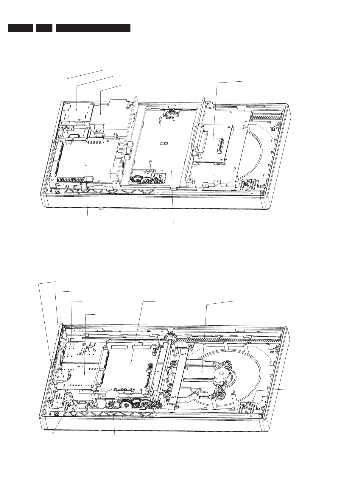
LOCATION OF PC BOARDS
Main Unit
PCBs on the Bracket
IPOD Board
USB Board
HDMI Board
SCART Board
Bracket
AV Board
Main Unit
PCBs on the Lower Level
IR Board
White LED Board
Front Key Board
Front Display Board
Motor Assembly
SD9.2 MPEG Board
DVD Mechanism
Door Close
Board
Door Open
Board
1.
Technical Specifications and Connection Facilities
Page 3
Technical Specifi
cations and Connection Facilities
TUNER MODULE
3139 785 32530
1.
EN 3
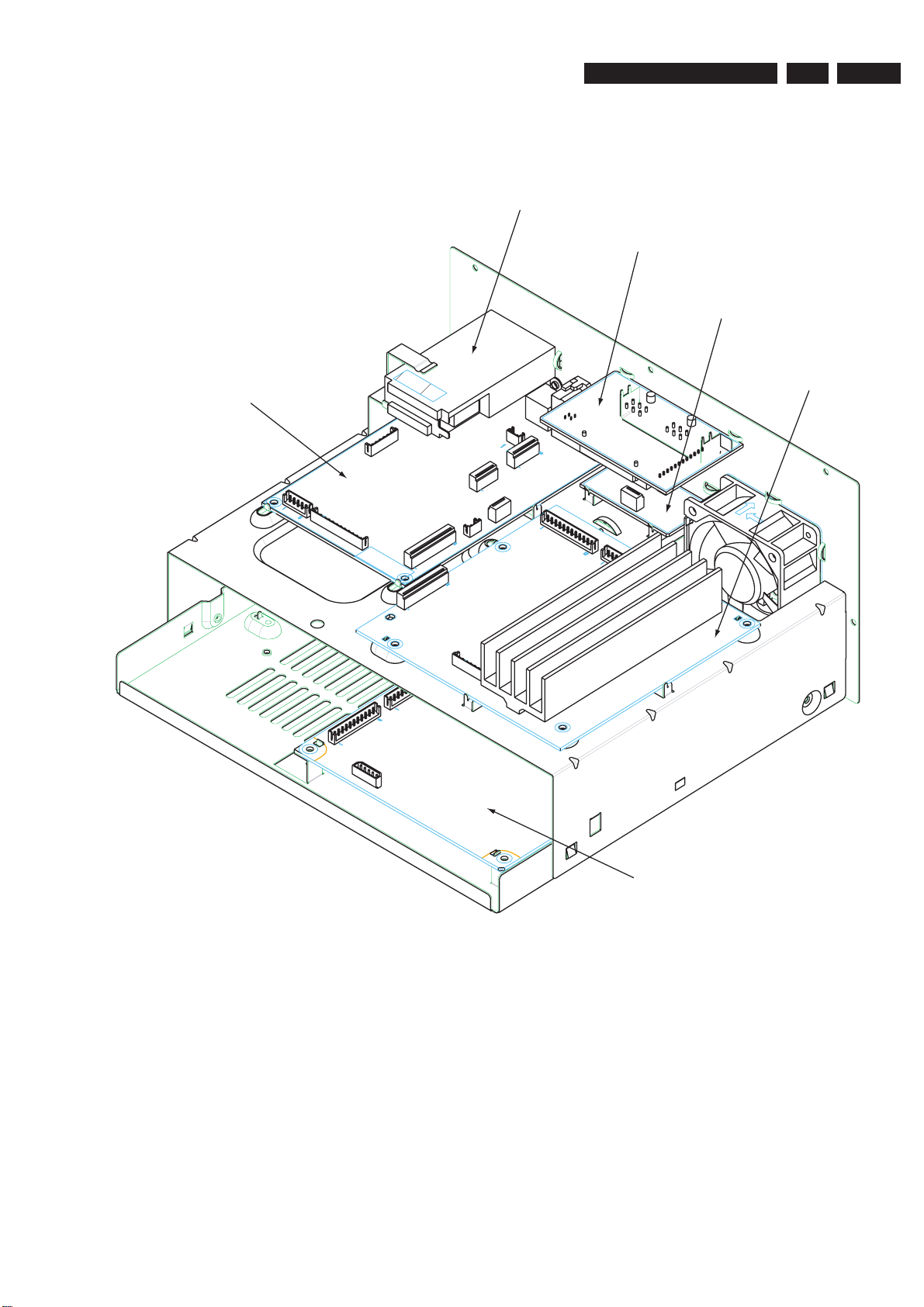
POWER BOX
AV BOARD
SPEAKER BOARD
AIO BOARD
AMPLIFIER MODULE
PSU
Page 4

EN 4
3139 785 325301.
1. Specifi cations
Technical Specifi
cations and Connection Facilities
1.1 General:
Mains voltage : 220-240V
Mains frequency : 50/60Hz
Power consumption : 120W
Low Standby Power: : < 1W
Dimension main unit : 370 x 76 x 242(mm)
(w x h x d)
1.2 Tuner
FM
Tuning range : 87.5-108MHz
Grid : 50kHz
IF frequency : 10.7MHz ± 25kHz
Aerial input : 75Ω coaxial
Sensitivity at 26dB S/N : < 7μV
Selectivity at 59/300kHz bandwidth : > 25dB
IF rejection : > 60dB
Image rejection : > 25dB
Distortion at RF=1mV, dev. 75kHz : < 3%
-3dB Limiting point : 8μV
Crosstalk at RF=1mV, dev. 67.5kHz : > 28dB
1.4 COMPACT DISC/VCD/DVD:
Video Decoding : MPEG-1/MPEG-2/
DivX 3/4/5/6, Ultra
Video DAC : 12 Bits
Signal System : PAL / NTSC
Video Format : 4:3 / 16:9
CVBS(SCART) Out
CVBS level : 1.0 ± 0.1V
Luminance S/N : >= 55dB
RGB/YUV Out
Amplitude : 0.7 ± 0.1V
S/N : >= 60dB
1)
Output terminals to be terminated with 75Ω
1)
p-p
1)
p-p
1.3 AMPLIFIER:
L/R output power : 1 x 70W type: 75W
Centre : 1 x 95W type: 100W
Surround : 1 x 70W type: 75W
Subwoofer : 1 x 95W type: 100W
Frequency response ±3dB : 150Hz-20kHz
Hum (Volume Minimum) : 200nW
Residual noise (Volume Minimum) : 40nW
Input sensitivity
Aux In : 1V ± 3dB at 39kΩ
Scart In (TV in): : 500mV ± 3dB at 39kΩ
Page 5
Measurements Setup, Service Aid & Lead Free Requirements
3139 785 32530
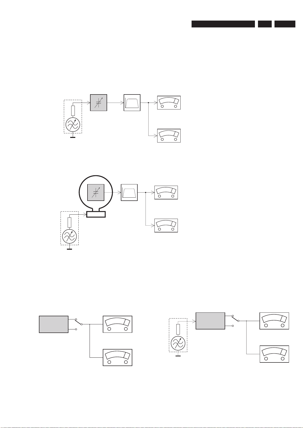
2. Measurements Setup, Service Aid & Lead Free Requirements
MEASUREMENT SETUP
Tuner FM
2.
EN 5
Bandpass
LF Voltmeter
e.g. PM2534
RF Generator
e.g. PM5326
DUT
250Hz-15kHz
e.g. 7122 707 48001
Ri=50Ω
S/N and distortion meter
e.g. Sound Technology ST1700B
Use a bandpass filter to eliminate hum (50Hz, 100Hz) and disturbance from the pilottone (19kHz, 38kHz).
Tuner AM (MW,LW)
RF Generator
e.g. PM5326
Ri=50Ω
DUT
Frame aerial
e.g. 7122 707 89001
Bandpass
250Hz-15kHz
e.g. 7122 707 48001
LF Voltmeter
e.g. PM2534
S/N and distortion meter
e.g. Sound Technology ST1700B
To avoid atmospheric interference all AM-measurements have to be carried out in a Faraday´s cage.
Use a bandpass filter (or at least a high pass filter with 250Hz) to eliminate hum (50Hz, 100Hz).
CD
Use Audio Signal Disc
(replaces test disc 3)
DUT
L
R
SBC429 4822 397 30184
S/N and distortion meter
e.g. Sound Technology ST1700B
LEVEL METER
e.g. Sennheiser UPM550
with FF-filter
Recorder
Use Universal Test Cassette CrO2 SBC419 4822 397 30069
or Universal Test Cassette
LF Generator
e.g. PM5110
Fe SBC420 4822 397 30071
DUT
L
R
e.g. Sound Technology ST1700B
S/N and distortion meter
LEVEL METER
e.g. Sennheiser UPM550
with FF-filter
Page 6
EN 6
3139 785 325302.
Measurements Setup, Service Aid & Lead Free Requirements
SERVICE AIDS
Service Tools:
Universal Torx driver holder .................................. 4822 395 91019
Torx bit T10 150mm ............................................. 4822 395 50456
Torx driver set T6 - T20 ......................................... 4822 395 50145
Torx driver T10 extended ...................................... 4822 395 50423
Compact Disc:
SBC426/426A Test disc 5 + 5A ............................ 4822 397 30096
SBC442 Audio Burn-in Test disc 1kHz ................. 4822 397 30155
SBC429 Audio Signals disc .................................. 4822 397 30184
Dolby Pro-logic Test Disc ...................................... 4822 395 10216
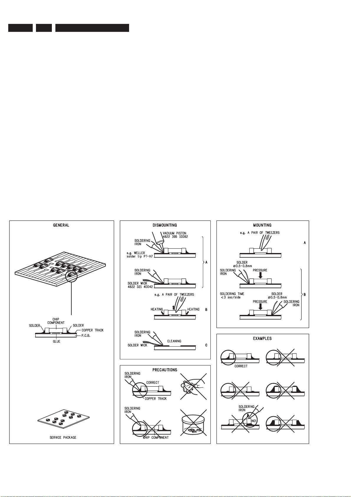
HANDLING CHIP COMPONENTS
Page 7
Measurements Setup, Service Aid & Lead Free Requirements
3139 785 32530
2.
EN 7
GB
All ICs and many other semi-conductors are
susceptible to electrostatic discharges (ESD).
Careless handling during repair can reduce life
drastically.
When repairing, make sure that you are
connected with the same potential as the mass
of the set via a wrist wrap with resistance.
Keep components and tools also at this
potential.
Tous les IC et beaucoup d’autres
semi-conducteurs sont sensibles aux
décharges statiques (ESD).
Leur longévité pourrait être considérablement
écourtée par le fait qu’aucune précaution n’est
prise à leur manipulation.
Lors de réparations, s’assurer de bien être relié
au même potentiel que la masse de l’appareil et
enfiler le bracelet serti d’une résistance de
sécurité.
Veiller à ce que les composants ainsi que les
outils que l’on utilise soient également à ce
potentiel.
F
WARNING
ATTENTION
GB
Complete Kit ESD3 (small tablemat, wristband,
connection box, extention cable and earth cable) ...........4822 3 1 0 10 6 7 1
Wristband tester ....................................................................4822 3 4 4 1 3 99 9
ESD
D
WARNUNG
Alle ICs und viele andere Halbleiter sind
empfindlich gegenüber elektrostatischen
Entladungen (ESD).
Unsorgfältige Behandlung im Reparaturfall kan
die Lebensdauer drastisch reduzieren.
Veranlassen Sie, dass Sie im Reparaturfall über
ein Pulsarmband mit Widerstand verbunden
sind mit dem gleichen Potential wie die Masse
des Gerätes.
Bauteile und Hilfsmittel auch auf dieses gleiche
Potential halten.
ESD PROTECTION EQUIPMENT:
NL
Alle IC’s en vele andere halfgeleiders zijn
gevoelig voor electrostatische ontladingen (ESD).
Onzorgvuldig behandelen tijdens reparatie kan
de levensduur drastisch doen verminderen.
Zorg ervoor dat u tijdens reparatie via een
polsband met weerstand verbonden bent met
hetzelfde potentiaal als de massa van het
apparaat.
Houd componenten en hulpmiddelen ook op
ditzelfde potentiaal.
Tutti IC e parecchi semi-conduttori sono
sensibili alle scariche statiche (ESD).
La loro longevità potrebbe essere fortemente
ridatta in caso di non osservazione della più
grande cauzione alla loro manipolazione.
Durante le riparazioni occorre quindi essere
collegato allo stesso potenziale che quello della
massa dell’apparecchio tramite un braccialetto
a resistenza.
Assicurarsi che i componenti e anche gli utensili
con quali si lavora siano anche a questo
potenziale.
WAARSCHUWING
I
AVVERTIMENTO
GB
Safety regulations require that the set be restored to its original
condition and that parts which are identical with those specified,
be used
Safety components are marked by the symbol
!
.
NL
Veiligheidsbepalingen vereisen, dat het apparaat bij reparatie in
zijn oorspronkelijke toestand wordt teruggebracht en dat onderdelen,
identiek aan de gespecificeerde, worden toegepast.
De Veiligheidsonderdelen zijn aangeduid met het symbool
!
F
Les normes de sécurité exigent que l’appareil soit remis à l’état
d’origine et que soient utiliséés les piéces de rechange identiques
à celles spécifiées.
Less composants de sécurité sont marqués
!
D
Bei jeder Reparatur sind die geltenden Sicherheitsvorschriften zu
beachten. Der Original zustand des Geräts darf nicht verändert werden;
für Reparaturen sind Original-Ersatzteile zu verwenden.
Sicherheitsbauteile sind durch das Symbol
!
markiert.
I
Le norme di sicurezza esigono che l’apparecchio venga rimesso
nelle condizioni originali e che siano utilizzati i pezzi di ricambio
identici a quelli specificati.
Componenty di sicurezza sono marcati con
!
CLASS 1
LASER PRODUCT
GB
Invisible laser radiation when open.
Avoid direct exposure to beam.
Osynlig laserstrålning när apparaten är öppnad och spärren
är urkopplad. Betrakta ej strålen.
SF
Avatussa laitteessa ja suojalukituksen ohitettaessa olet alttiina
näkymättömälle laserisäteilylle. Älä katso säteeseen!
DK
Usynlig laserstråling ved åbning når sikkerhedsafbrydere er
ude af funktion. Undgå udsaettelse for stråling.
S
Warning !
Varning !
Varoitus !
Advarse !
GB
After servicing and before returning set to customer perform a leakage
current measurement test from all exposed metal parts to earth ground to
assure no shock hazard exist. The leakage current must not exceed
0.5mA.
F
"Pour votre sécurité, ces documents doivent être utilisés par
des spécialistes agréés, seuls habilités à réparer votre
appareil en panne".
Page 8

EN 8
2.
3139 785 32530
2.1 Lead Free Requirements
Measurements Setup, Service Aid & Lead Free Requirements
Pb(Lead) Free Solder
When soldering , be sure to use the pb free solder.
INDENTIFICATION:
Regardless of special logo (not always indicated)
one must treat all sets from 1 Jan 2005 onwards, according next
rules:
Important note: In fact also products of year 2004 must be treated in
this way as long as you avoid mixing solder-alloys (leaded/ lead-free).
So best to always use SAC305 and the higher temperatures belong
to this.
Due to lead-free technology some rules have to be respected by the
workshop during a repair:
• Use only lead-free solder alloy Philips SAC305 with order
code 0622 149 00106. If lead-free solder-paste is required,
please contact the manufacturer of your solder-equipment.
In general use of solder-paste within workshops should be
avoided because paste is not easy to store and to handle.
• Use only adequate solder tools applicable for lead-free solder
alloy. The solder tool must be able
o To reach at least a solder-temperature of 400°C,
o To stabilize the adjusted temperature at the solder-tip
o To exchange solder-tips for different applications.
• Adjust your solder tool so that a temperature around 360°C
– 380°C is reached and stabilized at the solder joint. Heatingtime of the solder-joint should not exceed ~ 4 sec. Avoid
temperatures above 400°C otherwise wear-out of tips will rise
drastically and fl ux-fl uid will be destroyed. To avoid wear-out
of tips switch off un-used equipment, or reduce heat.
• Mix of lead-free solder alloy / parts with leaded solder alloy /
parts is possible but PHILIPS recommends strongly to avoid
mixed solder alloy types (leaded and lead-free).
If one cannot avoid or does not know whether product is leadfree, clean carefully the solder-joint from old solder alloy and
re-solder with new solder alloy (SAC305).
• Use only original spare-parts listed in the Service-Manuals.
Not listed standard-material (commodities) has to be
purchased at external companies.
• Special information for BGA-ICs:
- always use the 12nc-recognizable soldering temperature
profi le of the specifi c BGA (for de-soldering always use the
lead-free temperature profi le, in case of doubt)
- lead free BGA-ICs will be delivered in so-called ‘drypackaging’ (sealed pack including a silica gel pack) to protect
the IC against moisture. After opening, dependent of MSLlevel seen on indicator-label in the bag, the BGA-IC possibly
still has to be baked dry. (MSL=Moisture Sensitivity Level).
This will be communicated via AYS-website.
Do not re-use BGAs at all.
• For sets produced before 1.1.2005 (except products of 2004),
containing leaded solder-alloy and components, all needed
spare-parts will be available till the end of the service-period.
For repair of such sets nothing changes.
• On our website www.atyourservice.ce.Philips.com you fi nd
more information to:
BGA-de-/soldering (+ baking instructions)
Heating-profi les of BGAs and other ICs used in
Philips-sets
You will fi nd this and more technical information within the
“magazine”, chapter “workshop news”.
For additional questions please contact your local repair-helpdesk.
Page 9
Measurements Setup, Service Aid & Lead Free Requirements
3139 785 32530
2.2 Service Hints
2.2.1 Service Hints for Replacing Defective Loader
CAUTION
CHARGED CAPACITORS ON THE SERVO BOARD MAY DAMAGE THE DRIVE
ELECTRONICS WHEN CONNECTING A NEW DRIVE.THAT’S WHY, BESIDES THE SAFETY
MEASURES LIKE
• SWITCH OFF POWER SUPPLY
• ESD PROTECTION
ADDITIONAL ACTIONS MUST BE TAKEN BY THE REPAIR TECHNICIAN.
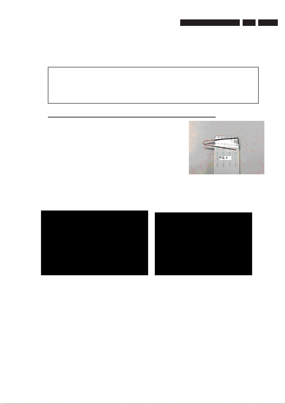
The following steps have to be done when replacing the defective loader :
1. Dismantling of the loader to access the ESD protection point if necessary.
2. Solder the ESD protection point*.
3. Disconnect fl exfoil cable from the defective loader.
4. Put a paper clip on the fl exfoil to short-circuit the contacts (fi g.1)
5. Replace the defective loader with a new loader.
6. Remove paperclip from the fl exfoil and connect it to the new loader.
7. Remove solder joint on the ESD protection point.
2.
EN 9
ATTENTION: The laser diode of this loader is protected against ESD by a solder joint which shortcircuits the laserdiode to ground.
Type 1 Type 2
(ESD protection point is accessible from top of loader) (ESD protection point is accessible from bottom of the loader)
*Only applicable for defective loader needed to be sent back to supplier for failure analysis and to support backcharging
evidence.
This is also applicable for all partnership workshops.
For proper functionality of the loader this solder joint must be remove after connection loader to the set.
Page 10

EN 10
Service Hints for Power Box Cable Dressing
2.2.2
The following procedures should be followed for Power Box Module
assembly after being repaired.
3139 785 325302.
Measurements Setup, Service Aid & Lead Free Requirements
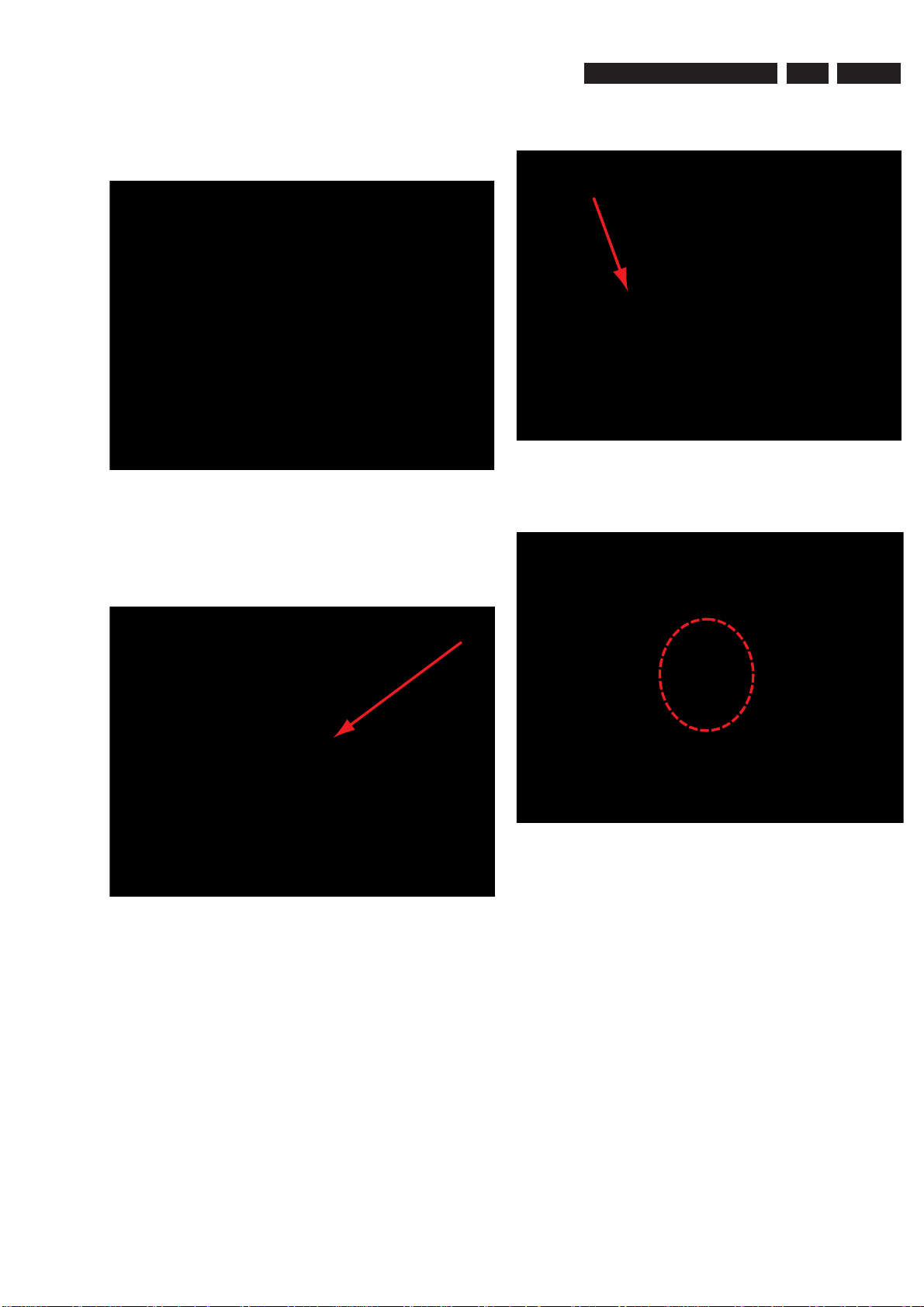
1) For the 5 and 12 poles cables to Audio BD, paste a tape
over them, ensuring it is fi rmly secured to the metal
chassis.
Figure 2-1
2) For the 8 pole cable between the PSU and TI amplifi er,
fold the cable as indicated, making it as close possible to
metal chassis.
3) Fold as indicated underneath the metal chassis for both
point 1) and 2). Note that the cables underneath should
be laid as close possible to the metal chassis also.
Figure 2-3
4) For the FFC cable between Audio BD and TI amplifi er,
fold as indicated, making it sure that the cable should be
outside of both boards.
Figure 2-2
Figure 2-4
Page 11
Measurements Setup, Service Aid & Lead Free Requirements
3139 785 32530
2.
EN 11
5) For the FFC cables from the Audio BD to Tuner/Speaker/
AIO BD, fold as indicated, hence, preventing them from
touching the Audio BD itself.
Figure 2-5
6) For the 9 pole cable linking from the Main Unit to the
Power Box, tuck it underneath the tuner and above the
4 pole cinch connector and also making it as close as
possible to the back metal plate.
7) For reference to point 6).
Figure 2-7
8) The cables should be tied as indicated.
Figure 2-6
Figure 2-8
Page 12

EN 12
3139 785 325302.
Measurements Setup, Service Aid & Lead Free Requirements
9) With reference to point 8), all cables should refrain from
touching or even getting near to the PSU.
Figure 2-9
10) Overview
11) Paste a tape over the subwoofer cable on the Tuner as
indicated. Secondly, the cable should be outside of the
Audio BD, along the edge of the metal chassis.
Figure 2-11
12) With reference to point 11).
Figure 2-10
Figure 2-12
Page 13

Measurements Setup, Service Aid & Lead Free Requirements
13) With reference to point 11). Note that the cable should
not be bent to the left across the Audio BD due to the
excess cable when the unit is being push back inside the
wooden Power Box.
Figure 2-13
3139 785 32530
2.
EN 13
14) With reference to point 11).
Figure 2-14
Page 14
EN 14
3139 785 325302.
Measurements Setup, Service Aid & Lead Free Requirements
Service Hints for Dismantling of Main Unit
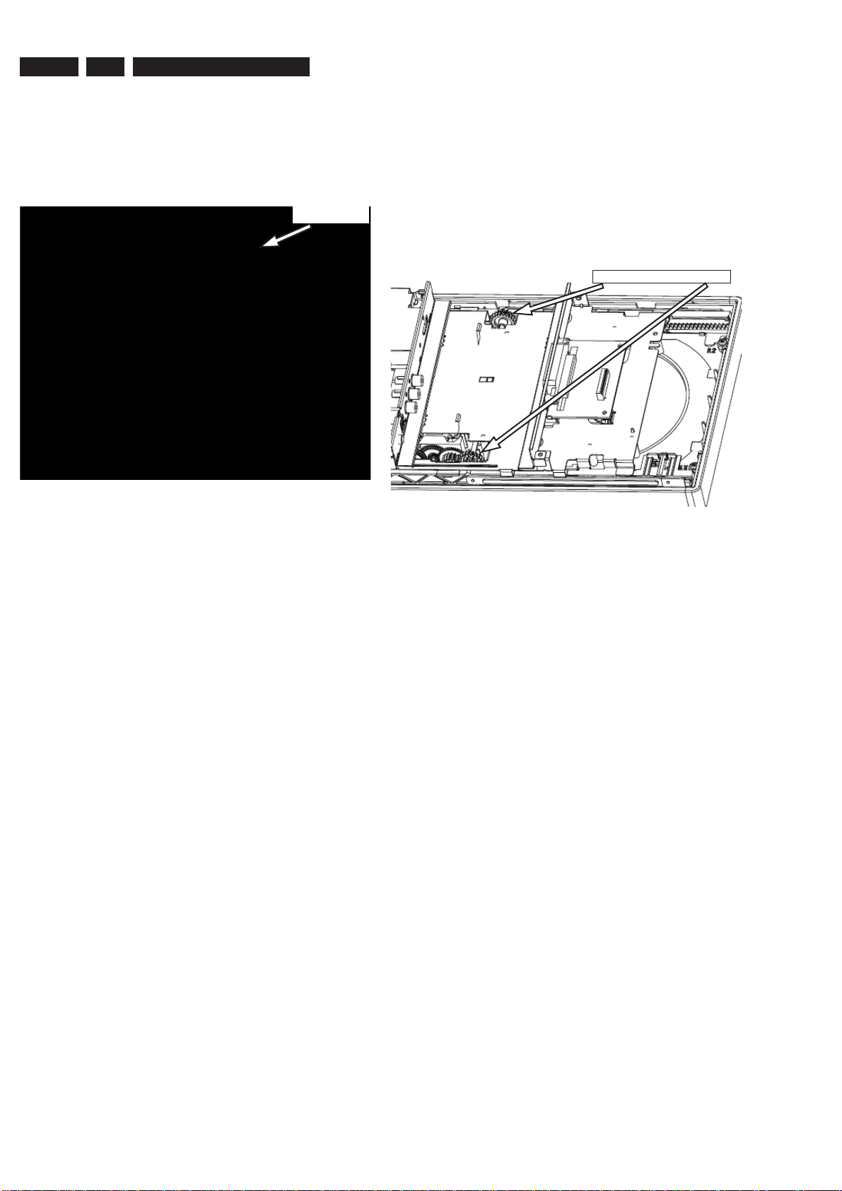
2.2.3
While dismantling of Main Unit, put the packing sheet under
the set as shown in the fi gure to prevent the face of the set
from scratches.
Figure 2-15
Packing Sheet
2.2.4 Manual Procedure to open the door
1. Remove the stand assembly (refer to chapter 4 for more
details)
2. Remove the cabinet Rear (refer to chapter 4 for more
details)
3. Manually slide the Top & bottom gear at Axial pipe to
manually open the door.
4. Remove the disc from the disc compartment.
Top & bottom gear at Axial pipe
Figure 2-16
Page 15
DVD HOME THEATRE SYSTEM
Quick Start Guide
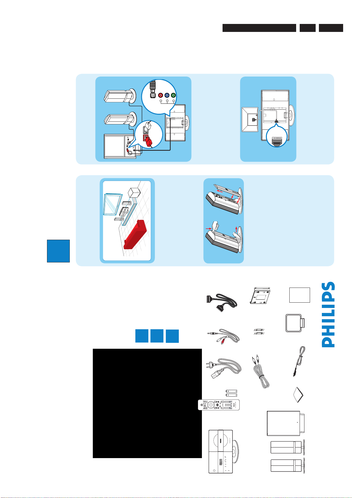
Connect
Set up
Enjoy
1
2
3
What’s in the box?
Main Unit
Remote Control
and 2 batteries
User
Manual
Speakers and subwoofer
FM wire
antenna
AM/MW
loop antenna
MP3 LINE-IN cable
2 sets of speak-
er wall mount-
ing brackets
HTS6600
Main unit wall
mounting
bracket
Micro bre
cleaning cloth
Scart Cable
Audio Cable
Power Cable
1
Connect
A
Placement
Proper speakers system placement is important to
ensure optimum sound performance.
RIGHT
LEFT
A Place the speakers at the normal listening ear level,
equal distance from the TV and face it straight ahead
towards the listening area.
B Place the subwoofer on the floor, at least one metre
away from the TV.
B
Remove rear cover from main unit
A
Carefully push down the rear cover from the top
and detach it from the main unit.
B
After all the connections have been made
(see the
following sections for details),
close the rear cover
by fitting the catches into the holes and pushing
upwards.
C
Connect the speakers and main unit
to subwoofer
TO DVD SYSTEM
AM/MW
FM/MW ANTENNA
SPEAKERS
COAXIAL
DIGITAL IN
AUX 1
AUX 2
RIGHT LEFT
FM 75
R
L
MAINS
SCART OUT
(TV1)
HDMI OUT
COMPONENT
VIDEO OUT
TO SUBWOOFER
TV AUDIO IN
(TV 2)
TO SUBWOO FER
Y
Pb
Pr
B
LEFTRIGHT
SPEAKERS
A
A
Connect the left speaker to the SPEAKER LEFT
socket and the right speaker to the SPEAKER
RIGHT socket at the rear of the subwoofer.
B
Connect the TO MAIN UNIT cable from the
subwoofer to the TO SUBWOOFER socket at the
rear of the main unit.
D
Connect the main unit to TV
SCART OUT
(TV1)
z
Connect a scart cable (supplied) from the
SCART OUT (TV1) socket on the main unit to the
SCART IN socket on your TV.
z
If your TV supports HDMI, connect the HDMI cable
(not supplied) from the HDMI OUT to the HDMI IN
socket on your TV.
Television
( rear)
Main unit (rear)
RIGHT
SPEAKER
LEFT
SPEAKER
Subwoofer (rear)
Directions for Use
3139 785 32530
3.
3. Directions For Use
The following except of the Quick Use Guide serves as an introduction to the set.
The Complete Direction for the Use can be downloaded in different languages from the internet site of Philips Customer care Center:
www.p4c.philips.com
(TV 2)
TV AUDIO IN
HDMI OUT
VIDEO OUT
COMPONENT
TO SUBWOOFER
SCART OUT
SCART IN
(TV1)
EN 15
AMBISOUND
Page 16
EN 16
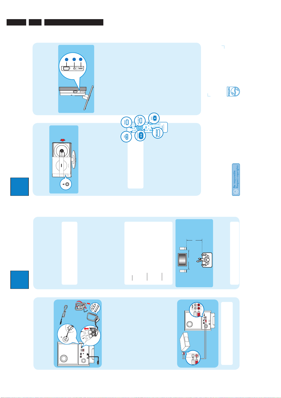
2
Set up
A
Finding the viewing channel
A Press 2 (STANDBY ON) on the main unit to turn
it on.
B Turn on the TV. Use the TVs remote control to
select the correct viewing channel.
Note To search for the correct viewing channel,
press the Channel Down button on the TVs remote
control repeatedly (or AV, SELECT,
° button) until
you see the Video In channel.
B
Setting up the speakers
When you turn on this unit for the rst time, the
speaker setup message appears on the TV.
A Press SETUP on the remote control to enter
‘General Setup Page’.
B Press cursor down to highlight { Ambisound
Setup } followed by pressing cursor right key.
C Select one of the options below and press cursor
right key.
{ Room Acoustics }
{ Hard } - for concrete or wooden walls.
{ Soft } - for curtains or an open space.
{ Speakers Distance }
{ Near } - ‘X’ is less than 1.2 metres (3.9 ft).
{ Default } - ‘X’ is between 1.2~2 metres (3.9~6.5 ft).
{ Far } - ‘X’ is more than 2 metres (6.5 ft).
{ Listening Position }
{ Near } - ‘Z’ is less than 2 metres (6.5 ft).
{ Default } - ‘Z’ is between 2~3 metres (6.5~9.8 ft).
{ Far } - ‘Z’ is more than 3 metres (9.8 ft).
Note The underlined options are the default setting.
TV
FRONT RFRONT L
X
Z
D Select a most suitable predefined setting and press
OK to confirm.
E Once complete, press SETUP to exit the menu.
Note Refer to the accompanying user manual
for other setup options.
E
Connect the radio antennas
Keep the antennas away from the electronic devices to
prevent unwanted interference.
A Connect the FM antenna to the inner pin of the
FM 75 socket. For optimum reception, extend the
wire and fix its end to the wall.
B Unfold the AM/MW loop antenna and fix the claw
into the slot. Push the tabs and insert the wires into
the AM/MW sockets
C Connect the power cable from subwoofer to the AC
power outlet.
F
Connect audio output from other
device (optional)
Use a red and white audio cables (not supplied) to
connect the AUDIO IN-AUX1 or AUX2 sockets on the
subwoofer to the AUDIO OUT sockets on the
connected device (for example, DVD recorder, VCR,
Cable/Satellite Box).
AUX 1
AUX 2
R
L
AUDIO OUT
AUDIO
OUT
Note Press AUX/DI on the remote control to
select ‘AUX1’ or ‘AUX2’ as the source you want to
listen to.
Main Unit
(rear)
Subwoofer (rear)
DVD recorder/
VCR/ Cable/
Satellite Box
Subwoofer (rear)
Listening
Position
Speakers Distance
FM antenna
AM/MW
antenna
3
Enjoy
Start disc playback
A Press ç to open the disc compartment.
B Place a disc with the disc label facing towards you.
C Press ç to close the disc compartment.
D Playback starts automatically.
E If the disc menu appears on the TV, use cursor keys
to select an option in the menu and press OK to
start playback.
z
To enjoy the powerful surround sound from the
speakers, press AMBISOUND on the remote
control to turn on the multi-channel surround
mode.
F Press
to stop playback.
Note When you press u button,
playback resumes from where it last
stopped. To start playback from the
beginning, you have to press ..
Playback other supported
devices
The connections to other devices are located at the left
side of the main unit.
Philips GoGear/Apple iPod
A Connect the Philips HTD7001 docking station (sold
separately) to
A
.
B Turn on your GoGear or iPod before dock it in the
correct cradle.
C Press DOCK to switch to ‘DOCK’ mode.
D Press PLAY on your GoGear or iPod.
Other portable audio player
A Use the supplied MP3 LINE-IN cable to connect the
headphone output socket on your portable audio
player to
B
.
B Press PLAY on your portable audio player.
C Press MP3 LINE-IN to listen to the playback.
USB device
A Insert your USB device to
C
.
B Press DISC/USB to switch to ‘USB’ mode.
C Press u to start playback.
D To stop playback, press DISC/USB to switch to
‘DISC’ mode. You can unplug your USB device now.
Need help?
User Manual
See the user manual that came with your Philips DVD Home Theatre System.
Online
Go to www.philips.com/support
2006 C Koninklijke Philips N.V.
All rights reserved.
12 NC 3139 245 25611
www.philips.com
Place the
disc here
3.
3139 785 32530
B
A
C
Directions for Use
A
FM 75
FM/MW ANTENNA
SPEAKERS
RIGHT LEFT
B
FM 75
AM/MW
AUX 2
AUX 1
L
R
COAXIAL
DIGITAL IN
MAINS
TO MAIN UNIT
C
FM 75
MW
FM/MW ANTENNA
AUX 2
AUX 1
L
R
COAXIAL
DIGITAL IN
MAINS
SPEAKERS
RIGHT LEFT
TO MAIN UNIT
Page 17
Dismantling Instructions & Service Positions
3139 785 32530
4.
4. Mechanical Instructions
Notes: The position numbers used in the instructions refer to the exploded view drawings in Chapter 8.
Follow the Service Hints in Chapter 2 for dismantling the Main Unit, replacing the defective DVD mechanism and the Power Box Cable
Dressing.
4.1 Dismantling of the Main Unit
4.1.1 Dismantling of USB, HDMI, AV, AVIO (SCART), and IPOD
boards
EN 17
1) Remove rear cover 170 and remove 2 screws to detach
the stand (161+162+163+164+165) as shown in Figure 1.
A
Figure 4-1
2) Remove 6 screws to detach Rear Cabinet 158 as shown
in Figure 2.
B
3) Remove 2 screws attached to the Bracket 146, and 1
screw attached to the AV plate 151 to remove the HDMI
Shield 154. Then remove 2 more screws attached to
the AV plate 151 to dismantle the HDMI board 1060.
Mounting screws for HDMI board are shown in fi gure 3.
C
Figure 4-3
4) Remove 2 screws to detach the USB board 1014 from the
Bracket 146 as shown in fi gure 4.
5) Remove 2 screws attached to the Bracket 146 and 3
more screws attached to the AV plate 151 to dismantle
the AV board 1020 as shown in fi gure 5.
Figure 4-2
D
Figure 4-4
Page 18

EN 18
6) In order to dismantle the IPOD board 1050, it is
necessary to remove the AV board fi rst. Then remove 3
screws to detach the IPOD board from the bracket 146 as
shown in fi gure 6.
3139 785 325304.
E
Figure 4-5
Dismantling Instructions & Service Positions
7) In order to dismantle the SCART board 1040, remove
2 screws attached to the Bracket 146, and 2 screws
attached to the SCART plate 152 as shown in fi gure 7.
G
F
Figure 4-6
Figure 4-7
Page 19
Dismantling Instructions & Service Positions
4.1.2 Dismantling of SD9.2 MPEG board
3139 785 32530
4.
EN 19
1) In order to dismantle the SD9.2 MPEG Board1070, it
is necessary to remove the Rear Cabinet, USB, HDMI,
SCART, and IPOD boards together with bracket 146. The
mounting screws for the bracket 146 are shown in
fi gure 8. Please keep in mind that the EMC Copper tape
153 shown in fi gure 9 should be at the correct place while
assembling the set after repair.
H
Figure 4-8
2) After removing the bracket 146, remove 4 mounting
screws to dismantle the SD9.2 MPEG Board 1070 as
shown in fi gure 10.
I
Figure 4-10
EMC Copper Tape
Figure 4-9
Page 20
EN 20
3139 785 325304.
Dismantling Instructions & Service Positions
4.1.3 Dismantling of the Front White LED, Front Display, Front
Key and IR Boards
1) To dismantle the boards of the Front Panel 1010, it is
necessary to remove the SD9.2 MPEG board1070. The
Front White LED board 1017 should be detached fi rst by
unscrewing the mounting screw. Then remove 3 mounting
screws to dismantle the Front Display board 1012 (One
screw is hidden underneath the FFC Foil 8010).
2) Remove 4 screws to dismantle the Front Key board 1013.
3) Only one screw should be removed to dismantle the IR
board 1018. The mounting screws for boards of the Front
Panel 1010 are shown in fi gure 11.
J
IR Board
J
Front Display Board
Front Key Board
J
White LED
Board
J
4.1.5 Dismantling of the Motor Assembly, Door open and Door
Close Boards
1) The Door Open 1015 and Door Close 1016 boards are
attached to the Rack-1 (117) without any mounting screw.
Detaching them can be done readily.
2) To dismantle the Motor Assembly (126+130+127+128+
129+125), remove 3 screws as shown in fi gure 12.
L
Figure 4-13
Figure 4-11
4.1.4 Dismantling of the DVD mechanism
1) To dismantle the DVD mechanism 1080, the FFC
dressing board should be removed fi rst by removing 2
mounting screws.
2) Then remove 4 screws and dismantle the DVD
mechanism as shown in fi gure 12. (Refer to “Service
Hints” in chapter 2 for replacing the DVD mechanism.)
K
Figure 4-12
Page 21
Dismantling Instructions & Service Positions
4.2 Dismantling of the Subwoofer Power Box
1) Loosen 5 screws at the base of the Subwoofer (as shown
in fi gure 14) and remove 5 screws at the back (as shown
in fi gure 15). Then pull out the Power Box Assembly.
3139 785 32530
4.
EN 21
M
Subwoofer Figure 4-14
N
Subwoofer Figure 4-15
O
Subwoofer Figure 4-17
3) Remove 4 screws for dismantling of the Amplifi er Module
1010 as shown in fi gure 18.
P
2) Remove1 screw for Tuner 1020, 3 screws for Speaker
Board 1060, and 1 screw for AIO board 1050 to detach
them from the Rear Plate 230. Remove 1 screw
attached to the Rear Plate 230 and 2 screws attached
to the bracket 236 for dismantling of the Audio Board
1040. Mounting Screws are shown in fi gure 16 and fi gure
17.
O
Subwoofer Figure 4-16
O
O
O
Subwoofer Figure 4-18
Page 22
EN 22
4) To dismantle the PSU 1030, it is necessary to dismantle
the Bottom Plate Assembly (1030 +161) from the Rear
Plate 230 (remove 3 screws as shown in fi gure 19) and
the bracket 236 (remove 3 screws from both sides of
the bracket 236 as shown in fi gure 20 and fi gure 21).
Then detach the Bottom Plate Assembly (1030 +161)
from the Rear Plate 230 and remove 4 screws detach the
PSU 1030 from the Bottom Plate 161 as shown in fi gure
22.
3139 785 325304.
Dismantling Instructions & Service Positions
R
Q
Subwoofer Figure 4-19
Q
Subwoofer Figure 4-20
Subwoofer Figure 4-22
Q
Subwoofer Figure 4-21
Page 23
Dismantling Instructions & Service Positions
4.3 Service Positions
3139 785 32530
4.
EN 23
HDMI Board
USB Board
Insulation Sheet
MPEG Board
Figure 4-23
Service Position 1
MPEG Board and HDMI Board
AV Board
Insulation Sheet
Remove Screw & Detach
Front Key
Board
Cutsheet & FFC Foil
Front Display Board
Service Position 3
Figure 4-25
Front Boards
IR Board
White LED
Board
SCART Board
IPOD Board
Figure 4-24
Service Position 2
AVIO (SCART), IPOD, USB and AV Boards
Amplifi er Module
Speaker Board
Insulation Sheet
Figure 4-26
Power Box Service Position 4
Amplifi er Module and Speaker Board
Page 24

EN 24
IO Board
3139 785 325304.
Speaker Board
Dismantling Instructions & Service Positions
AV Board
Insulation Sheet
Power Box Service Position 5
Figure 4-27
Audio Board, IO Board and Speaker Board
Insulation Sheet
Power Box Service Position 6
Figure 4-28
PSU
Page 25

5. Service Test Program
A
A
Service Test Program
3139 785 32530
5.
EN 25
To start Service Test Program,
power up the set, open the tray
with remote control or front
panel key and press 2,5,8 on the
remote control. The tray will close
by itself and the set will display
“S-Vxx-yy”.
Display shows
“SERVICE”
followed by ROM version
“S-Vxx-yy”
Main Menu
Display Test
key
"DisplayTest"
triggered?
y
ctivate and display
"Pattern1"
n
S refers to Service Mode
V refers to Version
xx refers to Software version number of BEA
(counting up from 01 to 99)
yy refers to Software version number of Front uP
(counting up from 01 to 99)
5.1 Display Test
Purpose:
This test is used to check the driving circuits, the display and whether there are
any short-circuits, open-circuits or any other defects.
Display test key =
Player:
Following display patterns are used to test the display and its connections to μP.
Pattern 1: Default: All display control pins are ON. All LEDs are ON
- to check the open-circuits
key
"DisplayTest"
triggered?
y
ctivate and display
"Pattern2"
key
" "
triggered?
y
Pattern 2: Alternate display control pins are on (Test Pattern: 0x55)
- to check the short-circuits on Data port
n
n
Page 26

EN 26
3139 785 325305.
Service Test Program
5.1.1 Reprogramming of DVD version Matrix
After repair, the customer setting and region code may be lost.
Reprogramming will put the set back in the state in which it has left
the factory, ie. with the default setting and the allowed region code.
Model Region Region Code TV Type
HTS 6600/05/12 EU 2 PAL
To reprogram do as follows:
1) Power up the set and select DISC source.
2) Open the tray with remote control or front panel key.
3) Press the following buttons on the Remote Control:
<9> <9> <9> <9> <AUDIO> <1> ...........for HTS 6600/05/12
4) The display shows ‘YYYY-ZZ’ and the tray will close.
YYYY = model number (eg. 8300, 8500, etc.)
ZZ = slash stroke version (eg. 01, 69, etc.)
5.1.2 Procedure to check software version
1) Power up the set and select DISC source.
2) Open the tray with remote control or front panel key.
3) Press “DISPLAY” button on the Remote control.
4) The TV screen will show:
SD9.2-Vxx 6600-zz dd
Servo:aaaaaaaa Reg:DD
HDCP PASS Fyy Pbb IGcc
xx = BEA Software Version
zz = Stroke Version (/05 or /12)
dd = Default stroke version region
aaaaaaaa = Servo Software Version
DD = User set region
HDCP PASS = HDCP key (for HDMI output) is encoded in the
set
yy = Front Software Version
bb = Powerbox Module Software Version
cc = iGIS module Software Version
5.1.3 Burning of fi rmware
1. Unzip the zip-archive attached with this service information.
2. Start the CD burning software and create a new CD Project
(Data disc) with the following settings:
a. File System: ISO9660
b. Format: MODE 2/XA
c. Recording format: Single Session (Track at once),
Finalized CD
3. Place the content of the zip-archive into the root directory of the
new CD project.
4. Burn the data onto a blank CDR or CDRW.
5.1.4 Procedure to upgrade the fi rmware
1. Power up the set and open tray.
2. Insert the prepared Upgrade CDROM and close the tray.
3. The OSD will Display:
“Upgrade fi le detected
Important: Do not unplug or switch off this device during the
upgrade
File Copying->Upgrading”
4. The tray will then open to allow the upgrade disc to be taken out.
5. Take out the upgrade disc. It may take one or two minutes to
complete the ERASE and WRITE processes.
6. When the upgrade process is successfully completed, the tray is
pulled in and the set will go to normal mode automatically.
5.1.5 Procedure to check the fi rmware version to confi rm
upgrading
1. Power up the set and open tray.
2. Press the <DISPLAY> button on the Remote Control.
3. The fi rmware version will be displayed on the top left hand corner
of the OSD.
5.1.6 Trade Mode
Trade mode is a feature that will block all set keys when enabled. It is
for dealers to prevent customers fromremoving disc, changing source
etc using the set keys.Rotary and Remote Control (RC) keys are still
allowed inTrade mode.
To activate Trade Mode:
1) Power up the set and select DISC source.
2) Open tray by press “OPEN/CLOSE” button on the set
or press and hold “STOP” button on the RC.
3) Then press buttons <2> <5> <9> on the RC.
4) The display shows ‘TRA ON’ and the tray will close.
Trade Mode is now enabled.
To deactivate Trade Mode:
1) Power up the set and select DISC source.
2) Open tray by press and hold “STOP”button on the RC.
3) Then press buttons <2> <5> <9> on the RC.
4) The display shows ‘TRA OFF’ and the tray will close.
Trade Mode is now disabled.
Note: ISO9660 is mandatory, UDF discs are not supported!
The fi nal CDROM must not contain any other data except
the fi le from the zip-archive.
Page 27

EN 27
3139 785 32530
A
B
C
D
E
F
G
H
I
J
A
B
C
D
E
F
G
H
I
J
1
2
3
4
56
7
8 9 10 11 12
13
13
1211
10
98
7
6
5
4
3
21
Front Display,
Class 3, 2-layer
MPEG Board
SD9.2
4-layer
94 x 105mm
DDR
SDRAM
4MX16
Flash
4MX8
E2PROM
SPDIF_OUT
RC6 (109)
Front_SDA (99)
Front_SCL (98)
Front_IRQ# (100)
S0 (202), S1 (203), SEL_0 (223), SEL_1 (222)
MUTE_CTRL_1 (97), MUTE_CTRL _2 (205)
Stby_Ctrl0
Interface between
KHM313 and Mono board:
Regulator
from
AM588S
3.3V + 1.8V
MOTOR
DRIVER
AM5888S
24P 0.5 FFC
H
6P PH V
KHM313AHC
5P PH V
USB Board
Class 3, 2-layer
1 +5V
2 D+
3 D4 GND
9P EH H to AV
1 GND
2 LD_DVD
3 NC
4 HFM
5 MD
6 LD_CD
7 VR_DVD
8 VR_CD
9 NC
10 E
11 VCC
12 VC
13 GND
14 F
15 B
16 A
17 RF
18 CD/DVD
19 D
20 C
21 T22 T+
23 F+
24 F-
1 SP2 SP+
3 L_SW
4 L_SW
5 SLED6 SLED+
Interface between Mono and AV board:
4P EH H
11P EH H
87CM74
MCU
VFD
11P EH V
SCL_1, SDA_1
16 Bit
ITU601
Buffer
74LVC125
Interface between Mono
and HDMI board:
SCART Connector
18P 1.25 FFC V
Current
Limiter
D+, D-
SCL_1(101), SDA_1(102)
MT1392
HDMI Con.
HDMI Board
Class 5, 2-layer
60x 60mm
I2C
V_CLK (166)
HSYNC (179)
VSYNC (181)
16 Bit YPbPr or
8bit ITU601
DDC_I2C
USB
Line_Det (226), TVin_Det (227)
MCU_IRQ# (224), MCU_TX (10 4), MCU_RX (103)
MT1389HD
4P EH V
SPDIF/I2S
Line_IN
1 Line_L
2 GND_A
3 Line_R
4 Line_Det
4P PH H to AV
USB_OC(199)
30P 1.25 FFC H + 21P 1.25 FFC H
6-ch Video Output ( CVBS/Y/C/Y/Pb/Pr)
Buffer
switch
I2S_0_1_2_3
50P 0.5 FFC H + 26P 0.5 FFC H
74LVC08
HDMI_MUTE
SCL_1, SDA_1
1 LOAD2 LOAD+
3 GND
4 TROUT
5 TRIN
Door Open
Class 3,
2-layer
1 MUTE_CTRL12
2 SCART_OUT_L
3 GND_A
4 SCART_OUT_R
5 GND_A
6 SCART_IN_L
7 GND_A
8 SCART_IN_R
9 GND_V
10 CVBS
11 GND_V
12 R
13 GND_V
14 G
15 GND_V
16 B
17 P8
18 P16
YUV
DC/DC + Regulator +
Power Switch
Video Sw
(Euro
only)
13P DIN
Audio
SW
2-Ch ADC
CS5340
18P 1.25 FFC H
SPDIF
IPOD/GG_L/R
LINE_L/R
9P EH H to
Front
18P 1.0 FFC H to
IPOD
SEL_0,SEL_1
S0
7P 1.25 FFC H
Pre-AMP
2-Ch DAC
CS4344
PBox_IRQ
SCART_IN_L/R
SCART_OUT_L/R
Transistor
S1
P8 P16
TV_L/R
TV_IN
Buffer
4P PH H to USB
I2C_1
30P 1.25 FFC H + 21P 1.25 FFC H
I
2
S
x
1
I2S
x 1
TVin_Det
CVBS
SCART_L/R
1 HDMI_MUTE
2 HDMI_RST
3 GND / SCL_1
4 HDMI_INT / SDA_1
5 SCL_0
6 SDA_0
7 GND
8 SPDIF
9 GND
10 PCM_LR
11 +5V
12 PCM_LsRs
13 +5V
14 PCM_LFe
15 +5V / +3V3
16 PCM_Cs
17 +5V / +1V8
18 PCM_LRCK
19 GND
20 SCLK
21 GND
22 PCM_MCLK
23 GND
24 Reserved
25 Reserved
26 Reserved
50P 0.5 FFC H + 26P 0.5 FFC H
1 PCM_MCLK
2 GND
3 PCM_BCLK
4 AUX_IN (DAC_STB)
5 PCM_LRCLK
6 GND
7 PCM_DATA0
8 GPO0 (S0)
9 GPO1 (S1)
10 GND
11 SPDIF_OUT
12 CVBS_REF
13 CVBS_DVD
14 G_REF
15 G_Y
16 B_REF
17 B_U
18 R_REF
19 R_V
20 GPIO_4 (SEL_0)
21 GPIO_5 (SEL_1)
22 SCL_0 (VSCK) (not used)
23 SDA_0 (VSDA) (not used)
24 MUTE_CTRL1
25 MUTE_CTRL2
26 GND
27 Y (not used)
28 GND
29 C (not used)
30 GND
1 GND
2 GPIO_6 (ACTIVE_STBY)
3 USB_OC
4 GND
5 SPDIF_IN (not used)
6 SCL_0 (not used)
7 SDA_0 (not used)
8 SYS_RST
9 GND
10 GPIO_1 (TVin_Det)
11 GND
12 +3V3
13 GND
14 SDA_1
15 SCL_1
16 GND
17 MCU_RX
18 MCU_TX
19 GPIO_3 (MCU_IRQ)
20 GPIO_2 (Line_Det)
21 GND
5P PH H
1 Reserved
2 Reserved
3 GND
4 Y9 (not used)
5 GND
6 Y8 (not used)
7 GND
8 Y7
9 GND
10 Y6
11 GND
12 Y5
13 GND
14 Y4
15 GND
16 Y3
17 GND
18 Y2
19 GND
20 Y1
21 GND
22 Y0
23 GND
24 V_CLK
25 GND
26 Reserved/27M
27 Reserved/GND
28 C9 (not used)
29 GND
30 C8 (not used)
31 GND
32 C7
33 GND
34 C6
35 GND
36 C5
37 GND
38 C4
39 GND
40 C3
41 GND
42 C2
43 GND
44 C1
45 GND
46 C0
47 GND
48 HYSNC
49 DE# (not used)
50 VYSNC
4P EH H
4P EH H
Front Key
Class 3, 2 layer
1 GND
2 STBY_LED
3 KEY1
4 KEY2
3P EH H
3P EH H
1 +5VSTBY
2 IR
3 GND
IR
STDBY
LED
IR Board
Scart Board (Euro Only)
Class 2, 1-layer
80 x 50mm
AV Board
Class 5, 2-layer
90 x 115 mm
2P EH
DIPMATE
2P EH
DIPMATE
1 TRIN
2 GND
Door Close
Class 3,
2-layer
HDMI_SW (228)
SYSRST (177)
SCL_0 (200)
SDA_0 (201)
1. +12V
2. GND
3 -33V
4 +5VSTBY
5 WAKEUP
6 SPDIF_IN
7 NC
8 NC
9 IRQ#
10 SDA_P
11 NC
12 SCL_P
13 CU_Det
18P 1.0 FFC H
22P Connector
Ipod/ GoGear I/F
CVBS, Y/C
Control li nes
IPOD_TX, IPOD_RX
+5V_IPOD (500mA)
+5V_GOGEAR (1.1A)
Current
Limiter
GOGEAR_I2C
MCU_I2C, MCU_IRQ
MCU_RST
MCU
A_L/R
IPOD/Gogear Board
Class 5, 2-layer 50 x 52 mm
Interface between IPOD/
Gogear and AV board:
1 A_L
2 GND_A
3 A_R
4 MCU_IRQ
5 MCU_RX
6 MCU_TX
7 +5V_IPOD
8 +5V_IPOD
9 GND
10 +3V3
11 GND
12 +12V
13 -12V
14 MCU_RST
15 GND
16 +5V
17 +5V
18 GND
1 LOAD+
2 LOAD-
2P EH H
1 GND
2 +12V
3 GND
4 -24V
5 +5VC
6 Pbox_IRQ
7 +5VL
8 +5VSTBY
9 STBY_CTRL0
1 +5VL
2 Front_SDA
3 Front_SCL
4 Front_IRQ
5 GND
6 RC6
7 GND
8 +5VC
9 STBY_CTRL0
or +5VC
10 SDA_1
11 SCL_1
ACTIVE_STBY (198)
ACTIVE_STBY
1 +5VSTBY
2 IR
3 GND
2P EH H
2P EH H
White
LED
1 LED
2 GND
3139-249-39421-130-A3-sh1.pdf 2006-09-08
6.
Block Diagram, Wiring Diagram
Main Unit Block Diagram
Page 28

EN 28
3139 785 32530
6.
Block Diagram, Wiring Diagram
AIO
BOARD
SPEAK BOARD
Primary 1
-33V
-12VA
+12VA
+5VL
+VCC
-VCC
Optical
Stby control
+12VL
PSU
Class D AMP
Sub
Analog
Signal
TO subwoofer
FR/FL, SR/SL
Cen
Analog
Signal
L
FR/SR/CEN
R
Sono-wave speaker
Sono-wave speaker connector( HTS6600
FR/FL/SL/SR/CEN
FL/SL/CEN
TO HTS8100 one Bar Speaker
+12VL
+5VL
12VL, +5VL, -33V, -12VA,
+12VA, GND, GNDA, STBY_PB,
5V_EVER, PWR_DN
Primary 2
GND
GNDA
+5V_EVER
GND
STBY_PB
TUNer
AUX1
AUX2
Sirius
HEF4052B
ADC
CS5340
ADC I2S
DATA
SPDIF REC
AK4113
DSP
DSPC56371AF180
1.25V
3V33V3
3V3
I2S_SPDIF_DATA
Coxial Input
SPDIF0
+5V6
-5V6
3V3
+5VL
SPDIFIN1
EEPROM
RDS
Micro Controller
SCL1, SDA1
TPA5050
TPA5050
Delay IC
Delay IC
I2S_D_Data
3V3
3V3
3V3
FM_DET(From Tuner)
+5VL
3V3
+3V3uP
I2S Data , I2S_MCLK, I2S_SCLK,I2S_LRCLK
FREQ_HOP, AMP_RST, AMP_ERR
AMP NTC
SEL0
SEL1
AUDIO BOARD
SPDIF1
RST_ADC
Buffer
74LVC1G125GW
OSC.
DSO751SV
EXTAL
Buffer
74LVC1G32GW
XT1
RST_AK4113
RST _DSP
RST_CIRCUIT
Buffer
74LVC1G32GW
I2S_MCLK
I2S_MCLK
I2S_MCLK
FAN_DET
FAN SWITCH
CIRCUIT
FAN_CTRL
FAN
INT_DSP
PWR_DN
TO Center Unit
CU_DET
Wake_UP
TU_RDS_CLK
TU_RDS_DATA
From Center Unit
12VL
+5V_EVER
TO Center Unit
AMP BOARD
12VL
+5V_EVER
TO HTS8100 one Bar Speaker
3139-249-40141-130-A3 pbx.pdf 2006-08-04
Power Box Block Diagram
Page 29

EN 29
3139 785 32530
6.
Block Diagram, Wiring Diagram
1YBTSV5+
9008
1 YBTSV5+
2RI 2 RI 11 LV5+
3DNG3DNG 01ADS_TNORF
9LCS_TNORF
1
DNG
8 QRI_TNORF
2
V21+
7DNG
3
DNG
66CR 4 V42- 1DNG 1 DNG
5DNG 5 CV5+ 2DEL_YBTS
4008
2DEL_YBTS
4 CV5+ 6QRI_xobP 31YEK 31YEK
30LRTC_YBTS
1
DEL_etihW 7 YBTSV5+42YEK 4 2YEK
2B1_ADS
2
DNG8LV5+
1 B1_LCS 9 0LRTC_YBTS
H HE P2
1+DAOL
1
+DAOL
2-DAOL
2
-DAOL
8008
1 NIRT
2DNG H HE P2
0048
1 -DAOL
2 +DAOL
1NIRT3TUORT
1
DEL_etihW
2DNG4DNG
2008
2
DNG
5NIRT
3008
1devreseR1devreseR
1008
2TSR_IMDH2devreseR
3
DNG
3DNG
4
TNI_IMDH
49Y
50_LCS5DNG
1devreseR 1 devreseR 6 0_ADS 68Y
2devreseR 2 TSR_IMDH 7 DNG
1
7DNG
1DNG 3 DNG3
DNG
8FIDPS
2
87Y
2DVD_DL 1 -DAOL 11 LV5+ 4)desu ton(9Y4
TNI_IMDH
9DNG
3
9DNG
3CN2+DAOL01 ADS_TNORF 5DNG 50_LCS 01RL_MCP
4
016Y
4 MFH3TUORT 9LCS_TNORF 6 )desu ton(8Y60_ADS 11 V5+
5
11 DNG
5DM 4 DNG8QRI_TNORF 7DNG 7 DNG 21sRsL_MCP
6
215Y
1DNG6
DC_DL 5 NIRT 7DNG 87Y8FIDPS 31 V5+
7
31 DNG
2 DVD_DL7DVD_RV 66CR 9 DNG9DNG 41 eFL_MCP
8
41 4Y
3CN8DC_RV 5DNG 016Y01RL_MCP
6108
513V3+/V5+
9
51DNG
4MFH 9 CN 4 CV5+ 11DNG11V5+ 61sC_MCP
01
613Y
5DM01E 3 0LRTC_YBTS 215Y21sRsL_MCP 718V1+/V5+
11
71DNG
6 DC_DL 11 CCV 2 B1_ADS 31 DNG31V5+ 81 KCRL_MCP
21
81 2Y
7 DVD_RV21 CV 1B1_LCS 41 4Y 41eFL_MCP 91DNG
31
91DNG
8DC_RV31
DNG
51 DNG 513V3+/V5+ 02KLCS
41
021Y
9CN
0108
41F 61 3Y 61sC_MCP 12 DNG
51
12DNG
01 E51
B
71 DNG 718V1+/V5+ 22KLCM_MCP
61
22 0Y
11CCV61
A
1KLCM_MCP 81 2Y81KCRL_MCP 32 DNG
71
32 DNG
21CV71 FR 2 DNG 91 DNG 91DNG 42
devreseR
81
42KLC_V
31
DNG
81DVD/DC 3 KLCB_MCP 021Y02KLCS 52devreseR/DNG
91
52DNG
41F 91 D4
)BTS_CAD(NI_XUA
12DNG12DNG 62
devreseR
62M72/devreseR
51
B
02C 5 KLCRL_MCP 220Y22KLCM_MCP 72DNG/devreseR
61
A
12 -T6DNG 32DNG 32DNG 82 9C
71 FR22 +T 7 0ATAD_MCP 42 KLC_V42
devreseR
92DNG
81DVD/DC32+F8)0S( 0OPG 52DNG52devreseR/DNG 038C
91D 42 -F9)1S( 0OPG 62
M72/devreseR
62
devreseR
13DNG
02C 01 DNG1DNG 72
DNG/devreseR
237C
12-T 11TUO_FIDPS2)6_OIPG(ETUM_IMDH 82)desu ton(9C
7108
33DNG
22+T1-PS 21 FER_SBVC3CO_BSU 92DNG 436C
32+F2+PS 31
DVD_SBVC
4 DNG 03 )desu ton(8C 53 DNG
42 -F 3 WS_L41FER_G5)DESU TON(NI_FIDPS 13DNG 635C
4 WS_L51
Y_G
60_LCS 237C 73 DNG
5 -DELS61
FER_B
70_ADS 33 DNG 834C
6+DELS71 U_B8
TSR_SYS 43 6C 93DNG
81FER_R9DNG 53DNG 043C
91V_R01)teD_niVT(1_OIPG 63 5C 14 DNG
5008
02
)0_LES( 4_OIPG
11DNG 73DNG 242C
1-PS 12
)1_LES( 5_OIPG
213V3+ 834C 34DNG
2 +PS 22
)desU toN( )KCSV( 0_LCS
31 DNG 93DNG 441C
3WS_L 32
)desU toN( )ADSV( 0_ADS
411_ADS 043C 54DNG
4 WS_L 42 1LRTC_ETUM51 1_LCS 14 DNG 64 0C
5-DELS 522LRTC_ETUM 61 DNG 24 2C 74DNG
6+DELS 62DNG 71 XR_UCM 34DNG
02
84CNYSH
72DESU TON( Y81XT_UCM 441C
12
94#ED
BSU
82 DNG 91 )QRI_UCM(3_OIPG 54DNG
22
05 CNYSV
1 DNG92)DESU TON( C 02 )teD_eniL(2_OIPG 64 0C
2+D03 DNG 12 DNG 74 DNG
6008
3 -D 84CNYSH
1 DNG 4 V5+ 94)desu ton(#ED
2 +D 05CNYSV
3 -D
4V5+
3108
4108
NI_ENIL
1L_eniL
7008
1L_eniL
2A_DNG2A_DNG 1KLCM_MCP1DNG
1
DNG
3R_eniL3R_eniL 2DNG2)6_OIPG(ETUM_IMDH
2
V21+
4teD_eniL4teD_eniL 3 KLCB_MCP 3 CO_BSU
3
DNG
4
)BTS_CAD(NI_XUA
4DNG 4V42-
5KLCRL_MCP 5 )DESU TON(NI_FIDPS 5 CV5+ 11 L_A
TRACS
6DNG60_LCS 6QRI_xobP 22 A_DNG
12LRTC_ETUM 7 0ATAD_MCP70_ADS 7 YBTSV5+ 33
R_A
2L_TUO_TRACS8)0S( 0OPG 8TSR_SYS 8LV5+ 4 4QRI_UCM
12LRTC_ETUM3A_DNG 9)1S( 0OPG 9DNG 9 0LRTC_YBTS 55
XR_UCM
2L_TUO_TRACS4R_TUO_TRACS01DNG01)teD_niVT(1_OIPG 66
XT_UCM
3A_DNG5A_DNG11TUO_FIDPS11DNG 77 DOPI_V5+
4R_TUO_TRACS 6L_NI_TRACS21 FER_SBVC213V3+ 88 DOPI_V5+
5 A_DNG
1108
7A_DNG 31
DVD_SBVC
31 DNG 1 L_A 99 DNG
6 L_NI_TRACS8R_NI_TRACS41 FER_G 411_ADS 2A_DNG 0101 3V3+
7A_DNG9V_DNG51
Y_G
511_LCS 3 R_A 11 11DNG
8R_NI_TRACS01SBVC61
FER_B
61DNG 4QRI_UCM 2121V21+
9 V_DNG11V_DNG 71U_B71XR_UCM 5
XR_UCM
3131V21-
01SBVC 21
R
81FER_R81XT_UCM 6
XT_UCM
41Y_S / SBVC
11V_DNG31V_DNG 91 V_R91 )QRI_UCM(3_OIPG 7DOPI_V5+ 51DNGV
21
R
41
G
02
)0_LES( 4_OIPG
02)teD_eniL(2_OIPG 8 DOPI_V5+
5108 41
61TSR_UCM
31V_DNG51
V_DNG
12
)1_LES( 5_OIPG
12DNG 9DNG 71C_S
41
G
61B 22
)desU toN( )KCSV( 0_LCS
013V3+
51
81DNG_V/DNG
51
V_DNG
71
8P
32
)desU toN( )ADSV( 0_ADS
11DNG
61
91V5+
61B 81
61P
42 1LRTC_ETUM
1
V21+ .1
21V21+
71
02V5+
71
8P
522LRTC_ETUM
2
DNG .2
31V21-
81
12DNG
81
61P
62 DNG
3
V33- 3 41
TSR_UCM
OIVA
72DESU TON( Y
4
YBTSV5+ 4 51
DNG_V/DNG
1A_DNG82DNG
5
PUEKAW 5 61
V5+
2TFEL_VT92)DESU TON( C
6
NI_FIDPS 6 71
V5+
3A_DNG03DNG
7
CN 7 81
DNG
4THGIR_VT
8
CN 8
5V_DNG
9
#QRI 9
6SBVC
01
P_ADS 01
7
V_DNG
11
CN 11
21
P_LCS 21
31
teD_UC 31
ALPSID TNORF
Y
reyal-2 ,3 ssalC
mm05 X mm041
KHM313AHC
USB
Board
Line_IN
24P 0.5 FFC H
6P PH V
4P EH V
SYEK TNORF
3 ssalC
reyal-2
4P EH H
4P EH H
4P EH H
Scart Board (Euro Only)
2-layer 80mm X 50mm
18P 1.25 FFC V
18P 1.25 FFC H
DRAOB VA
reyal-2 , 3 ssalC
mm511 X mm09
4P PH H
4P PH H
7P 1.25 FFC H
DRAOB GEPM
2.9DS
reyal-4
mm501 X mm09
H HE P11
V HE P11
H HE P9
26P 0.5 FFC H
50P 0.5 FFC H
26P 0.5 FFC H / 40P 0.5 FFC H
50P 0.5 FFC H / 22P 0.5 FFC H
H CFF 52.1 P03
H CFF 52.1 P12
H CFF 52.1 P03
H CFF 52.1 P12
H HE P9
18P 1.00 FFC H
NID P31
21P 1.00 FFC H / 18P 1.00 FFC H
IGIS Board
2-layer
50mm X 52mm
DRAOB IMDH
reyal-2
mm011 X mm07
V HP P5
ESOLC_ROOD
2P EH H
RI
3P EH H
H HP P5
ETAMPID HE P2
NEPO_ROOD
YART
ROTOM
2P EH H
2P EH H
3P EH H
3139-249-39991-132-A3-sh1.pdf 2006-09-08
Main Unit Wiring Diagram
Page 30

EN 30
3139 785 32530
6.
Block Diagram, Wiring Diagram
From Center unit -13P min din cable To mains socket
8009 only for Eu and AP
1301 1400
10P FFC 1.25 AD 10P FFC 1.25 AD 1201 1200 5P EH VERTICAL 5P EH VERTICAL
1 GND 10 GND
9P EH
RJ45
1
+5VL
1
+5VL 1 MAINS
2 VCC 9VCC
HTS6600/8100
HTS5950
2 +12VL 2 +12VL
2MAINS
3 NC/RDS 8 NC/RDS 1
WakeUp
SCL_P
3
GND
3
GND
4 TU_R 7 TU_R 2
IRQ
GND
4
+5VSTBY
4
+5VSTBY
5 TU_STEREO 6TU_STEREO 3
SCL
SDA_P
5
-33V
5
-33V
1 SELECTOR
6
TU_L
5
TU_L
4
SDA
GND
2 SELECTOR
7
TU_TUNED
4
TU_TUNED 5
Cu_det
SPDIF
1401 12P EH VERTICAL
3 SELECTOR
8
SDA
3
SDA 6
-33V IRQ#
12P EH VERTICAL
1
+5VL
9 SCL 2 SCL
7
+5VSTBY VOL+
1
+5VL
2
GND
10 PORT_S 1 PORT_SEL
8
+12V VOL-
2
GND
3
+5VL
9
GND
3
+5VL
4
+5VL
1402
4
+5VL
5
GND
2H EH /Vertical
5
GND
6
+12VA
8P EH VERTICAL
1 LED
6
+12VA
7
GND_A
1
+VCC
2 GND
7
GND_A
8
-12VA2+VCC8-12VA9STBY AMP
3
+VCC
9
STBY AMP
10
PWR_DN
4
GND_A
10
PWR_DN
11
+12VL
5
GND_A
11
+12VL
12
GND
6
GND_A
12
GND
7
+12VL
8
+5VL
1202
20P 1.25 FFC AD
1304 1 GND
TCS7927 2 I2S_SCLK
1 +5V (900mA)
3 GND
2
+5V_EN
4 I2S_LRCK
3
SR_RX
5 GND
4
SR_TX
6I2S_MLK
5 GND
7 GND 1.25 FFC AD
6 SR_L
8 I2S_FLR 1GND
8P EH VERTICAL
7 GND_A
9 GND 2I2S_SCLK
1
+VCC
8 SR_R
10 I2S_CSW 3GND
2
+VCC
9
GND 11 GND 4 I2S_LRCK
3
+VCC
10
GND 12 I2S RLR 5GND
4
GND_A
11
GND 13 GND 6 I2S_MCLK
5
GND_A
SIRIUS
14 SDA 7GND
6
GND_A
15 SCL 8I2S_FLR
7
+12VL
16 GND 9GND
8
+5VL
17 AMP_RST 10 I2S_CSW
18 ERR 11 GND
1203
19 NTC 12 I2S RLR
6P EH
20 FREQ_HOP 13 GND
1 BOOT 14 SDA
2UART_RX 1207 (hts8100/6600) 15 SCL
3 UART_TX 1 FRONT
16 GND
4 GND 2 SUR
17 AMP_RST
5 UART_CTS
3
CEN
18 ERR
6 UART_RTS
4 GND 19 NTC
Remarks : HTS8100/6600- 1207 is inserted;
20 FREQ_HOP
HTS5950-1206 is inserted.
1208 and 1206 is at same location,
optional insertion.
1302
1206( hts5950)
5P FFC 1.25 8P FFC 1.25
1
SPDIF_IN1 Remarks : HTS8100/6600/5950- 1305 is inserted; 1
FRONT
1101 2 GND HTS6000-1302 is inserted. 2
SUR
12P EH
7P FFC 1.25 3 SPDIF_IN0 3
CEN
1 SR-
1
SPDIF_IN1
4
GND 4 GND 2SR+
2 GND
5
SPDIF_OPT 5
3.3V VREF
3SL-
3 SPDIF_IN0
6
GND6SPK_CTRL
4SL+
4 GND
7
+5VL7SPK_DET0
5R-
5 SPDIF_OPT 8
SPK_DET1
6R+
6
GND
1305
7L-
7
+5VL
1 SPDIF_IN1 1204 8L+
8002 2 GND 2P EH V 9CTR- 4P EH
Remarks : HTS8100/6600/5950; 4P FFC 1.25 1103 3 SPDIF_IN0 1FAN 10 CTR- 1 SUB-
1
SPDIF_IN1
4
GND 2 GND 11
CTR+ 2 SUB-
2 GND 12 CTR+ 3 SUB+
inserted
3
SPDIF_IN0 4SUB+
4
GND
2P EH 1102
1 SPDIF_IN1
2
GND To 8100/6600 sub woofer
12P DIPMATE
1 SR-
12P EH
4P FFC 1.25
2SR+
1SR-
1
FRONT
3SL-
2SR+
2
SUR
4SL+
3 SL- 3
CEN
5
R-
4SL+ 4 GND 6
R+
5
R-
7
L-
6
R+
8
L+
7
L- 9CTR-
8
L+ 10 CTR-
From Center unit -13P min din cable 9CTR-
11
CTR+
10 CTR-
12
CTR+
11
CTR+
1403
12
CTR+
1401 1405 1406
Sirius receiver
To 8100 speaker
1103 is inserted;
HTS6000-1101 is
AUDIO BOARD (APB)
CLASS-5, 2 LAYER
90X150
PSU Module
TI AMPLIFIER
Module
TUNER
Module
8100/6600 SPEAKER PCB
AIOB PCB
L Sono SP con. (6600)
R Sono SP con.
(6600)
Center
FLSL
SR
FR
coaxial
Optical
1100
7100
8000
8003
8004
8006
8005
8008
8007
8001
8010
8012
TO Fan
To power box LED
3139 111 02721
FFC FOIL 10P/080/10P AD
3139 241 03171
3139 241 03161
FFC FOIL 04P/100/04P AD
FFC FOIL 07P/100/07P AD
3139 111 03091
CBLE MIS 05P/220/05P MIS 26OS
CBLE MIS 12P/180/12P MIS 260S
3139 241 03181
3139 111 01831
CBLE MIS 08P/220/08P MIS 26OS
FFC FOIL 20P/080/20P AD
3139 241 01921
FFC FOIL 04P/080/04P AD
3139 110 36051
CBLE MIS 12P/080/12P OE 26OS
3139 241 03091
3139 241 03151
CBLE MAINS ASSY 100MM
3139-249-40151-132-A3 pbx.pdf 2006-08-04
Power Box Wiring Diagram
Page 31

EN 31
3139 785 32530
7
Main Unit
Front Board: Circuit Diagram (Part 1)
Circuit Diagram and PWB Layout
RESET
VASS
INT3
INT2
INT4
INT5
XTIN
XTOUT
SCL
V
P9<0:7>
V
SO1
5
6
7
6
5
4
3
2
29
28
27
26
25
24
2
3
4
TC1
SCK0
0
1
2
3
4
5
6
SI1
SCK1
DVO
TEST
VKKVDDVAREF
14
13
12
11
10
9
8
SDA
22
TC3
P1<0:7>
STOP
P2<0:2>
SI0
SO0
P3<0:2>
AIN
31
30
P5<0:3>
PD<0:4>
V3
P6<0:7>
V
P7<0:7>
V
P8<0:7>
23
16
21
20
19
18
17
P4<0:7>
AIN
1
0
15
VSS
PDO
2
1
XTAL
P0<0:7>
PPG
PWM
TC4
13
12
11
10
7
INT0
INT1
TC2
F
G
H
I
1100 A1
1102 B1
1104 F1
1105 F5
1106 C5
1108 A10
1109 I4
1110 H9
1111 G1
2100 C2
1234567 8 9 10 11 12 13
12345678910
11 12 13
A
B
C
D
E
F
G
H
I
A
B
C
D
E
2101 B3
2102 B3
2103 C3
2104 C3
2105 C4
2106 D1
2107 D2
2108 E2
2109 E2
2110 E2
2111 F1
2112 F1
2113 F1
2114 F2
2115 F2
2116 F3
2117 D3
2118 D4
2119 D4
2120 D5
2121 C4
2122 D5
2123 C6
2124 C6
2125 C7
2126 F5
2127 F5
2131 I11
2132 H11
2133 H12
2134 G11
2135 G13
2136 F11
2137 E11
2138 E11
2140 F13
2141 F13
2142 E13
2143 E13
2144 E13
2145 E13
2146 E13
2147 E13
2148 E13
2149 D13
2150 D13
2151 D13
2152 D13
2153 D13
2154 D13
2155 D13
2156 B1
2157 B1
2158 B2
2159 A3
2160 B3
3100 A3
3101 B3
3102 C4
3103 D2
3104 D2
3105 D3
3106 F2
3107 F2
3108 D3
3109 D4
3110 C5
3111 C5
3112 D5
3113 F5
3114 F5
3115 G4
3116 G4
3117 G5
3118 G5
3120 I5
3121 I5
3123 I11
3124 H11
3125 H12
3126 I12
3127 I13
3128 G11
3129 F11
3130 G13
3131 G13
3132 F12
3133 E12
3134 C10
3135 B10
3136 B13
3137 C13
3138 H6
3139 A3
3140 A3
3141 G4
3142 G4
3143 G4
3144 H5
4101 F3
6100 C4
6101 D3
6103 I11
7100 C6
7101 A2
7102 D4
7104 I5
7106 F11
7107 F11
7108 F12
7109 H12
7110 A2
F101 A1
F102 A1
F103 B1
F104 B1
F105 B1
F106 B1
F108 C1
F110 C1
F111 C1
F112 C1
F113 C1
F114 E1
F115 E1
F116 E1
F117 E1
F118 E1
F119 E1
F121 E1
F122 F1
F123 F1
F124 F1
F125 I4
F126 I4
F127 H9
F128 H9
F129 H9
F130 E6
F131 B10
F132 B13
F133 C6
F134 C6
F135 C6
F136 F10
F137 G10
8213
R074
4213
K01
0n1
8112
K22
10K
4413
3143
7313
2R2
7R4
4313
F111
4013
3K3
+12V
3K3
5013
F129
R086
F130
0213
9K3
0212
0n1
8013
R033
2313
22p
2126 2140
100p
8
9
S9B-EH
1102
1
2
3
4
5
6
7
PDZ6.8-B
6100
BC327-25
7107
613SAB
1016
100p
2151
F123
F110
n001
2012
1
2
B-6.5ZDP
3016
1109
S2B-EH
1014
8P649P
74
6012
V61u74
51P761P
2P043P144P245P346P447P
54
1CI
4
2CI
15
1P
93
01P8411P9421P
055
31P
41P
6
322G223G12
4G
025G9
1
6
G
817G718G61
9G
42
1G
51
01G4111G3121G2131G1141G0151G961G
11F
21F
2
31F4541F
35
72
12F
22F
62
32F9242F
82
LCD
16-BT-145GN
1108
1
p033
0012
n001
2312
100p
2155
F132
6112
n001
p74
3012
2154
100p
5
1
2
3
4
F133
1111
S5B-EH
100p
2149
100p
2147
2R2
6313
F112
7013
3K3
330R
3133
3110 10R
F122
7012
n001
7
21
3
K
01
3125
1K2
3K3
6013
3013
820R
3K3
3101
7108
BC847BW
100p
2153
+5VSTBY
6113
7K2
3109
10K
F105
F114
9012
p74
YBTSV5+
n74
5212
3140
22K
7101
BC847B
867K23
3118
1K0
5011
F131
10R
3111
F135
F116
3113 10R
V61u001
3212
2112
p74
1112
p74
100p
2145
35V22u
2134
u22
8312
V53
F121
1012
V53u74
F134
2K7
3139
p74
0112
F119
7109
BC847BW
F128
2150
100p
2136
22u 35V
BC337-25
7106
2
3
4
5
6
7
8
9
1104
S11B-EH
1
10
11
F108
7312
n33
K01
2013
1K0
3112
3142
33R
33R
3141
F137
F136
BC847B
7104
2152
100p
2148
100p
2u2
7112
K01
0313
3117
F115
2K7
R051
8313
13
93
83 04877
9
8
68
69
70
71
72
73
74
75
76
77
10
58
59
60
61
62
63
64
65
66
67
47
48
49
50
51
52
53
54
55
56
57
34
35
36
37
41
42
43
44
45
46
24
25
26
27
28
29
30
31
32
33
16
17
18
19
20
21
22
14
12
11
23
79
80
1
2
3
4
5
6
15
Φ
MICROPROCESSOR
TMP87PM74ZFG
7100
BC847B
7110
n33
9112
100p
2141
S4B-EH
1100
1
2
3
4
n001
4012
F102
0K1
3213
10R3114
R074
9213
3112
p74
p22
1212
5012
u22V53
2R2
5313
VFIL_DC
F124
F117
3126
47K
F106
F104
100p
2143
7K2
5113
5112
V61u74
F126
F125
2127
22p
7u4
3312
3100
10K
2146
100p
2142
100p
F103
F118
F101
p22
2212
10K
3121
7K4
1313
7102
BC847BW
1110
S3B-EH
1
2
3
+5VSTBY
1106 8M0
4112
p74
F127
1312
2n2
8512
n001
n001
7512
6512
n001
9512
n001n001
0612
8012
F113
5312
p74
4212
n001
p22
2144
100p
ioKey2
P16
SCL
SDA
+5VL
FIL1
SCL
SDA
V42-
VFIL_DC
2LIF
+5VSTBY
+5VC
RC6
Front_IRQ
Front_SCL
G1
G2
G3
G4
G5
G6
G7
G8
G9
G10
G11
G12
G13
G14
G15
G16
+5VC
+5VSTBY
21P31P
41P
51P
2P3P4P5P6P
7P8P9P
Low_STBY_LED
+5VSTBY
Low_STBY_LED
StdbyLED
+5VSTBY
IR
IR
SCL_1B
Front_SDA
+5VL
SDA_1B
1G
01G
11G
21G
31G
41G
51G
61G
61P
2G3G4G5G6G7G8G
9G 1P
01P
1
1
P
G8
G9
G10
G11
G12
SCL_1B
SDA_1B
SwaveLED
+5VC
+5VSTBY
G13
G14
G15
G16
Active_LED
Pbox_IRQ
Front_IRQ
LV5+
+5VL
ioKey1
ioKey2
+5VSTBY
+5VL
STBY_CTRL0
1LIF
FIL2
G1
G2
G3
G4
G5
G6
G7
zHk04
Front_SDA
Front_SCL
RC6
STBY_CTRL0
40kHz
IR
ioKey1
StdbyLED
SwaveLED
P15
P14
P13
P12
P11
P10
P9
P8
P7
P6
P5
P4
P3
P2
P1
YBTSV5+
V42-
+12V
Pbox_IRQ
-24V
3139-243-35885-130-01-a2.pdf 2006-12-22
Page 32

EN 32
3139 785 32530
7.
Front Board: Circuit Diagram (Part 2)
Circuit Diagram and PWB Layout
6
7
NC
ADR
IC
2
1
2
SDA
SCL
0
P
INT
0
1
2
3
4
5
A
B
C
D
E
F
G
H
A
B
C
D
E
F
G
H
1200 E1
1201 G1
1202 G2
1203 G3
1204 G3
123456789101112
123456
789101112
1205 H1
1206 H2
1207 H3
1208 A2
2200 G4
2201 H3
2202 B5
2203 A6
2204 B6
2205 C6
2206 C6
2207 D6
2208 E6
2209 F6
2210 G6
2211 C4
3200 F2
3201 F2
3202 F3
3203 H2
3204 H2
3205 B4
3206 B4
3207 A6
3208 B6
3209 B6
3210 C6
3211 D6
3212 E6
3213 F6
3214 G7
3215 F8
3216 F8
3217 F8
3218 F8
3219 F9
3220 F9
3221 F9
3222 A10
3223 B10
3224 C10
3225 D10
3226 E10
3227 E10
3228 F10
3229 A10
6200 E2
6201 A6
6202 B6
6203 B6
6204 C6
6205 D6
6206 E6
6207 F6
6208 G6
6209 A10
6210 A10
6211 B10
6212 C10
6213 D10
6214 E10
6215 E10
6216 F10
6217 A8
6218 B8
6219 C8
6220 D8
6221 D9
6222 E9
6223 F9
7201 B4
7202 A7
7203 B7
7204 B7
7205 C7
7206 D7
7207 E7
7208 F7
7209 G7
F201 E1
F202 E1
F203 E1
F204 E1
3229
820R
7u4
4022
820R
3222
7123
6K5
1223
9123
2K2
2K2
0223
9K3
33n
2211
51
47n
2202
19
20
1
3
8
13
18
2
4
5
6
7
9
10
11
12
14
16
17
IOEXP
PCF8574TS/F3
7201
7206
BC847B
3200
220R
7022
7u4
6205
BAS316
7204
BC847B
p001
0022
5022
7u4
9022
7u4
6207
BAS316
4
BC847B
7207
6021
HHKS
1
2
3
7u4
8022
1
2
3
4
BAS316
6206
2
3
4
HHKS
4021
4
3021
HHKS
1
HHKS
2021
1
2
3
6203
BAS316
8123
9K3
9K3
6123
5123
9K3
3224
820R
820R
3223
3226
820R
7202
BC847B
S4B-EH
1200
1
2
3
4
613SAB
613SAB
3226
2226
613SAB
613SAB
1226
0226
613SAB
613SAB
9126
8126
6201
BAS316
613SAB
7126
BAS316
6204
7u4
6022
BC847B
7203
BC847B
7205
3225
BAS316
6208
820R
7209
LTW-M670
6216
BC817-25
6214
LTW-M670
LTW-M670
6213
6212
LTW-M670
LTW-M670
6211
6210
LTW-M670
LTW-M670
6209
6202
LTW-M670
6215
BAS316
1
2
3
4
5
1208
S5B-EH
7208
BC847B
220R
3203
270R
F202
3204
F201
LTL-816EELC
6200
HHKS
7021
1
2
3
4
1
2
3
4
3201
1021
HHKS
p001
270R
1022
3211
100K
100K
3210
3209
100K
100K
3208
F204
3207
100K
F203
820R
3227
3228
820R
100K
3214
3206 10R
10R3205
3022
7u4
7u4
0122
3
4
HHKS
5021
1
2
3213
100K
100K
3212
390R
+5VL
+5VL
3202
SCL
SDA
+5VL
+5VL
SCL
SDA
3139-243-35885-130-02-a2.pdf 2006-12-22
Page 33

EN 33
3139 785 32530
Front Board: Circuit Diagram (Part 3)
7
Circuit Diagram and PWB Layout
Front Board: Circuit Diagram (Part 4)
123
A
1302
1
+5V
D-
2
D+
3
GND
4
WH04D-1
From Mono Board
T301
T302
T303
T304
+5V
5301
600R
5302
600R
B
V52u01
2032
n001
1032
4301
4302
1303
1
2
3
4
56
E-CK0382-001
+5V
D-
D+
GND
A
B
1302 A1
1303 A3
1304 D1
1305 D3
2301 B2
2302 B2
2303 E2
2304 E2
2305 E2
4301 A2
4302 B2
5301 B2
5302 B2
5303 D1
5304 D1
5305 D1
T301 A1
T302 A1
T303 B1
T304 B1
T305 D1
T306 D1
T307 D1
T308 D1
123
1-D20HW
1
2
A
1401
1400 B2
1401 A1
1403 B3
1404 C2
F401 B3
F402 B3
F403 B3
F404 B3
F405 B3
A
C
D
E
Line_L
GND
Line_R
Line_Det
1304
1
2
3
4
S4B-PH-K
From AV Board
T305
T306
T307
T308
GND
<,,,annot_deleted,>
5304 600R
1400
1
B
USB Circuit
1
1305
600R5303
600R5305
4032
5032
3032
p01
p01
p01
3
11
10
2
4
5
6
EJ-3507P-102(PHA)
C
C
D
123
2
SPVF
4
3
S2B-PH-K
2
1
1404
3139-243-35885-130-04-a4.pdf 2006-12-22
F401
F402
F403
F404
F405
S5B-PH-K
1403
5
4
3
2
1
B
C
E
Line In Circuit
3139-243-35885-130-03-a4.pdf 2006-12-22
123
Page 34

EN 34
3139 785 32530
7.
Circuit Diagram and PWB Layout
Front Board: Circuit Diagram (Part 5)
Front Board: Circuit Diagram (Part 6)
123
A
A
1500 B2
1501 B1
F501 B2
F502 B2
12
1600 A1
6600 A2
F601 A1
F602 A1
B
C
1501
1
2
S2B-EH
F501
F502
3139-243-35885-130-05-a4.pdf 2006-12-22
1500
SPVF
123
B
C
1600
1
2
S2B-EH
F601
F602
L-174A2PWC-A-TNB5-19
6600
AA
3139-243-35885-130-06-a4.pdf 2006-12-22
1
2
Page 35

EN 35
3139 785 32530
7
Circuit Diagram and PWB Layout
Front Board: Circuit Diagram (Part 7)
Front Board: Circuit Diagram (Part 8)
123
A
1701
1
2
3
S3B-EH
F701
F702
F703
3701 100R
1701 A2
2701 A2
2702 A3
3701 A2
7701 B2
F701 A2
F702 A2
F703 A2
F704 B2
A
A
1072
2072
n001
7u4
123
1801
1
2
3
S3B-EH
F801
F802
F803
100R3801
A
2082
n001
1082
7u4
1801 A1
2801 A2
2802 A3
3801 A2
7801 B1
F801 A2
F802 A2
F803 A2
F804 B2
B
C
VS
F704
3
1
2
B
7701
OUT
GND
TSOP4836
C
3139-243-35885-130-07-a4.pdf 2006-12-22
123
B
C
7801
VS
OUT
GND
TSOP4836
F804
3
1
2
B
C
3139-243-35885-130-08-a4.pdf 2006-12-22
123
Page 36

EN 36
3139 785 32530
Door Close 3139-243-36126-top-a4.pdf_2007-02-13
Front Board
PWB Layout: Door Close (Top view)
Door Close 3139-243-36126-bot-a4.pdf_2007-02-13
Front Board
PWB Layout: Door Close (Bottom view)
7.
Circuit Diagram and PWB Layout
Page 37

EN 37
3139 785 32530
Door Open 3139-243-36086-top-a4.pdf_2007-02-13
Front Board
PWB Layout: Door Open (Top view)
Front Board
PWB Layout: Door Open (Bottom view)
Door Open 3139-243-36086-bot-a4.pdf_2007-02-13
7
Circuit Diagram and PWB Layout
Page 38

EN 38
3139 785 32530
Front Display 3139-243-35876-top-a3.pdf_2007-02-13
Front Board
PWB Layout: Front Display (Top view)
7.
Circuit Diagram and PWB Layout
Page 39

EN 39
3139 785 32530
Front Board
PWB Layout: Front Display (Bottom view)
Front Display 3139-243-35876-bot-a3.pdf_2007-02-13
7
Circuit Diagram and PWB Layout
Page 40

EN 40
3139 785 32530
Front Board
PWB Layout: Front Key (Top view)
Front Key 3139-243-35896-top-a3.pdf_2007-02-13
7.
Circuit Diagram and PWB Layout
Page 41

EN 41
3139 785 32530
Front Board
PWB Layout: Front Key (Bottom view)
Front Key 3139-243-35896-bot-a3.pdf_2007-02-13
7
Circuit Diagram and PWB Layout
Page 42

EN 42
3139 785 32530
Front Board
PWB Layout: IR (Top view)
IR 3139-243-36366-top-a4.pdf_2007-02-13
Front Board
PWB Layout: IR (Bottom view)
IR 3139-243-36366-bot-a4.pdf_2007-02-13
7.
Circuit Diagram and PWB Layout
Page 43

EN 43
3139 785 32530
Front Board
PWB Layout: White LED (Top view)
White LED 3139-243-36316-top-a4.pdf_2007-02-13
Front Board
PWB Layout: White LED (Bottom view)
White LED 3139-243-36316-bot-a4.pdf_2007-02-13
7
Circuit Diagram and PWB Layout
Page 44

EN 44
3139 785 32530
Front Board
PWB Layout: USB (Top view)
USB 3139-243-36096-top-a4.pdf_2007-02-13
Front Board
PWB Layout: USB (Bottom view)
USB 3139-243-36096-bot-a4.pdf_2007-02-13
7.
Circuit Diagram and PWB Layout
Page 45

EN 45
3139 785 32530
7.
Circuit Diagram and PWB Layout
AV Board: Circuit Diagram (Part 1)
COM
OUTIN
VCC
V5.1
SYNC
COMP
OUT
VFB
OSC
BOOT
GND
INH
SS
B
C
D
E
F
G
H
I
A
B
C
D
E
F
G
2101 D3
2102 C4
H
2345678910111213
123
2103 C2
2104 C2
2105 B2
2106 B2
2107 B2
2108 B3
2109 C3
2110 B5
I
1100 C1
1102 A8
1104 C13
1105 A12
2100 D3
1
2125 F3
2126 F1
2127 G4
2128 H5
2129 G4
2130 B8
2131 C5
2132 D6
2133 D7
2134 G9
3100 C7
3101 C7
3102 C8
3103 C8
3104 D2
13
A
3132 C5
3133 F2
3134 D9
3135 D10
3136 D10
4100 H9
5100 C4
5103 F5
5104 H8
5105 H10
6101 C8
6102 G5
6103 D6
6104 E7
6105 F6
7101 E3
7102 H10
7103 F3
7104 F8
7105 G8
7106 C5
7109 D5
7110 D11
F100 B2
F101 B2
F102 C2
F103 C2
F104 C2
F105 C2
F106 C3
456789101112
F119 B7
F120 B8
F121 D12
F122 D12
F123 D12
F124 D12
2123 G2
2124 G2
F127 E12
F128 E12
F129 E12
F130 C12
F131 D12
F132 D12
F133 B8
3129 G5
3131 G8
2111 B6
2112 B6
2113 D2
2114 D9
2115 C9
2116 B11
2117 B7
2118 B7
2119 B11
2120 B12
2121 B8
2122 G6
6109 B7
7100 C8
F125 D12
3105 E3
3106 D5
3108 F8
3109 A5
3123 G5
3126 G9
3127 G6
3128 H5
F126 E12
F107 D3
F108 D2
F109 D1
F110 A7
F111 A6
F112 A6
F113 A6
F114 A12
F115 A11
F116 B12
F117 A12
F118 A8
6106 F6
6107 H9
6108 F8
7K4
6313
BC847BW
7101
7109
BC817-25W
4100
F129
K01
8213
9013
K22
PBSS5220T
7104
BC807-25
7100
3103
1K0
n074
4212
1112
p74
8012
V61u074
2016
63SS
1u0
2125
470R
3132
1016
21C-483XZB
MBRA210L
6104
10K
3126
5100
60R
SCL02SCL17
SDA03 SDA1 6
VCC
8
GND_D
7110
PCA9515ADP
EN5
GND
4
NC
1
F113
F117
GND_D
GND_D
3212
7n2
F104
p074
6012
9
K01
4313
13
2
3
4
5
6
7
8
LAC1315-0102FC
1100
1
10
11
12
5313
7K4
F102
BC817-25W
7106
GND_D
F115
F121
7112
p074
F128
V01u074
2212
F127
F124
6112
p074
7212
p022
7
8
9
6106
MBRA210L
S9B-EH
1102
1
2
3
4
5
6
120u
5103
F112
8112
p074
F106
F119
47p
2101
2105
470p
F100
0312
p074
BZX384-B5V6
6103
p74
0112
5105
60R
F125
F107
3112
p074
47K
3105
F116
3101
1K0
F120
F133
3
4
5
6
7
1105
1
2
R065
440055-7
7213
5K1
9213
1313
7K4
6108
MBRA210L
p074
u001V61
4112
2112
p74
1212
F122
F110
0212
p074
4012
p74
2132
47u16V
F111
F131
R065
2103
100p
8013
47p
2100
F132
21
3
4
5
6
7
8
9
13
14
15
16
17
18
19
2
20
1104
HLEM21R-1
1
10
11
12
6105
MBRA210L
16V 47u
2131
V61u74
3312
9012
p074
F118
F114
820R
3106
3313
K22
BC847CW
7105
6212
n022
GND_D
n22
u74V61
5112
8
9
13
8212
1516 17
11
1
2
319
20
18
10
12
45
6714
GND_D
7103
L4973D5.1
Φ
REGULATOR
LD1086D2T33
1
32
7102
F108
3102
1K0
p074
9112
GND_D
F103
F123
6109
BAT760
2012
p074
V61u074
F126
7012
F101
GND_D
4312
1K9
3213
n001
GND_D
S1D
6107
60R
5104
F130
F105
4013
K022
3100
10R
F109
2129
220n
PBox_IRQ#
+5VL
+5VC
-25V
-25V
+5VL
+12V
+12VC
+5VSTBY
+3V3
+12VC
+5VC
+3V3_D
+5VC
+5VL
STBY_CTRL0
+5VSTBY
+12V
Active_stby
+5VC
+12A
+5VA
SDA_1
SCL_1
Line_Det
HOST_IRQ
HOST_SCL
HOST_SDA
+3V3
TVin_Det
MCU_RST
Active_stby
USB_OC
+12V
PBox_IRQ#
SDA_1
SCL_1
+3V3_D
+5VSTBY
SPDIF
STBY_CTRL0
-25V
+12V
-12V
3139-243-35837-130-01-a2.pdf 2007-01-19
Page 46

EN 46
3139 785 32530
7
Circuit Diagram and PWB Layout
AV Board: Circuit Diagram (Part 2)
EN
B
D
1A
2A
2C
2D
S
S
S
S
1D
A
IN
VCC
GND
1C
D
1B
2B
C
1204 A1
1205 C1
12345
2216 C12
2217 C12
2218 C8
2219 C12
3200 E3
3201 E3
13
A
B
C
D
3208 A8
3209 A9
3210 F2
3211 F3
3212 F3
3213 F4
F
G
H
I
I
1200 A2
1201 C12
1202 C11
1203 F12
10 11 12 13
12
2212 A8
2213 A9
2214 B12
2215 C12
4201 E7
4202 F7
4203 E8
4204 F8
4205 F8
4206 D13
3202 E4
3203 E4
3204 E5
3205 E6
3206 C7
E
EXT RGB
0 - 0.4V :
3214 G4
3215 G3
3216 G5
3217 G5
3218 H5
A
P16
2200 E3
2201 E3
6789
2206 E9
2207 E9
2208 E9
2209 F9
2210 F10
2211 F10
3220 A3
3221 D5
3222 D5
4200 E7
F201 A3
F202 A3
F203 A3
F204 B3
F205 B3
F206 B3
4207 C6
4208 D6
5200 D5
5201 D4
5202 D4
3207 C7
S0 = 0 SCART RGB
CVBS
6200 F9
6201 F10
6202 F11
3219 H4
2202 E4
2203 E4
2204 E6
2205 E6
1
7202 G4
7203 H5
7204 H5
F200 A3
F221 C10
F222 D10
F223 D10
F224 D10
F225 D11
F226 D11
F207 B3
F208 C3
F209 C3
F210 C3
F211 C3
5203 A8
F213 B3
F214 B3
F215 B3
7200 C7
7201 F4
F217 C11
F218 C10
F219 C10
F220 C10
1
1
RGB
YUV
Mode
-
F227 E11
F228 E11
F229 F11
F230 F11
F231 B3
F212 C3
TV BCAST
4: 3 DVD
16 : 9 DVD
0 - 2V :
9.5-12V :
F216 C11
4: 3 DVD
16 : 9 DVD
1 - 3.0V :
S1
P8
S0
X
0
0
1
0
F232 B3
0
4.5 - 7V :
Aspect Ratio
S0 = 1 YUV
S2
0
9
B
C
D
E
F
G
H
3456789101112
TV BCAST
16 : 9 DVD
4: 3 DVD
0
1
1
0
0
1
10
2
3
4
5
6
7
8
10FNM-STK-A
1205
3215
10K
F223
7K2
31234123
F217
8K1
4208
4207
1023
R051
2
3
4
5
6
7
8
9
1204
HLEM16R-1
1
10
11
12
13
14
15
16
6R8
F231
3221
F218
3222
4R7
V
F214
2
4200
7203
1
3
4205
BC847BW
4204
R051
3023
2022
p74
2023
R051
5202
1u8
9022
p001
1
2
3
4
5
6
F210
LPR6520-P910F
1203
F230
F219
F229
F204
F201
F200
F202
V
1122
p001
p74
3022
5201
1u8
5200
1u8
47p2219
F228
p74
1022
F226
F225
V
4203
4023
R051
F215
47p2215
1
3
2
2
BC847BW
7201
7204
BC847BW
1
3
GND_A
F207
F211
V
1u8
5203
2214 47p
4022
p74
F205
F212
F216
p74
6022
47p2216
K01
0123
10K
3212
4202
n001
8122
p001
0122
p74
5022
V
F232
3
30
4
5
6
7
8
9
20
21
22
23
24
25
26
27
28
29
11
12
13
14
15
16
17
18
19
2
HLEM30R-1RLF
1200
1
10
F224
K22
6123
8
9
2026
51C-483XZB
15
16
17
18
2
3
4
5
6
7
1
10
11
12
13
14
1202
HLEM18R-1
R074
8123
R051
0023
R051
5023
F206
F208
F203
F209
F213
8022
p74
p74
7022
470R
3206
F220
3122
p74
2217 47p
10K
3219
R051
R051
8023
9023
1
3
2
p74
2122
BC847BW
7202
4206
F227
7123
R57
K01
1123
3220
10R
51C-483XZB
1026
0026
51C-483XZB
7023
F222
K33
F221
0022
p74
4201
V
6
10
13
16
9
12
15
8
1
2
5
11
14
3
VIDEO SW
Φ
TS5V330PW
7200
4
7
1
2
3
4
5
6
7
S2
HLEM7R-1
1201
SEL_1
MUTE_TV
PCM_BCLK
PCM_OUT
S0
CVBS
G_Y
B_U
R_V
PCM_MCLK
SEL_0
SPDIF
S1
PCM_LTRT
PCM_LRCLK
S2
P16
SCART_IN_L
SCART_IN_R
MUTE_SCART
SCART_OUT_L
SCART_OUT_R
S0
S0
P8
CVBS
+5VC
R_V
B_U
G_Y
+12VC
S2
S1
+5VC
P8
P16
+5VC
3139-243-35837-130-02-a2.pdf 2007-01-19
Page 47

EN 47
3139 785 32530
7.
Circuit Diagram and PWB Layout
AV Board: Circuit Diagram (Part 3)
G4
0
3
2
VDD
VEE VSS
1
0
3
2
1
4X
030
1
SDIN
SCLK
GND
VQ
FILT+
AOUTL
AOUTR
DEM
LRCK
MCLK
VA
M
AINL
MCLK
RST
1
0
AINR
GND REF_GND
VQ
LRCK
SCLK
FILT+
SDOUT
VLVDVA
7308 A7
7309 B12
7310 C11
F300 A2
F301 A2
F302 A2
F303 B2
F304 B2
F305 B2
F309 B2
F310 C2
F311 C2
F312 C2
5304 B3
5305 C3
4303 A12
4304 A6
4305 A6
5300 A3
5302 I13
5303 D9
6303 A7
5306 C3
5307 C2
5308 C3
6301 A12
6302 D10
3357 I8
3358 I5
3359 I10
3360 I10
3362 A12
3363 A11
3325 D3
3327 E8
3366 A7
3367 C10
3368 A11
F313 C2
F314 C3
F315 C3
F316 C2
F317 E2
F318 D2
F319 E2
F324 E2
3345 G5
3346 H8
3347 H5
3348 H10
3349 H10
3351 H3
MCU_RST
MCU_IRQ
+5V
+12V
6306 B9
6307 B10
7302 C7
7303 D11
7304-1 H8
7304-2 I8
7306 H13
7307 A12
3315 C7
3318 D8
3320 B4
3321 D10
3323 D11
3324 D11
A IPOD
GND
3329 E4
3330 E14
3331 E13
3370 B9
3372 B4
3373 B4
3374 B4
3375 B2
3377 E10
4301 C3
4302 D10
2368 D2
2369 A12
3300 A4
3301 A4
3302 A3
3304 A4
2337 H11
2338 H9
GND
3353 H8
3354 H13
3355 I3
3356 A13
2350 I10
2351 F11
2352 F12
2353 F12
2354 I13
2355 I13
SDA_XM(TX)
VGND
+5V_iPod
3332 E3
3334 E4
3335 E7
3337 F7
3338 F4
3340 F5
3342 G4
3344 G8
2329 F6
2330 F3
2332 G6
2333 G3
2335 G8
2336 H7
+5V
-12V
2339 H9
2340 H10
2341 H8
+5V_iPod
3305 A5
3306 D2
3308 B11
3311 B6
3313 C6
3314 C7
2311 D8
2312 D9
2313 D12
2314 D8
2315 D10
2316 D10
GND
GND
2317 D4
2318 E9
2356 I13
2362 D12
2363 A8
2364 A8
2365 H11
2366 I11
2367 A3
7 8 9 10 11 12
123
1303 B2
2342 H12
2343 H12
2344 H12
2345 I8
2346 I13
2347 I11
2348 I9
2349 I9
67891011
3V3
B
C
D
E
F
G
H
I
1300 E1
1301 A2
12
2319 E10
2320 E13
2321 E13
2322 E13
2323 E3
2325 E4
2326 E3
2328 F7
SCL_XM(RX)
A IPOD
13
2300 A2
2301 A3
2302 A3
2303 C4
2304 C2
2308 C6
2309 A12
2310 E13
45
14
A
B
C
D
E
F
G
H
I
A
13 14
123456
GND_A
1
3
2
p86
3332
4
13
3
7307
BC857BW
78
12
1
14
5
15
2
11
MDX
HEF4052B
7302
10
9
6
16
6232
1
2
3
4
5
6
7
8
9
p86
HSJ0914-01-140
1300
GND_A
GND_A
GND_A
3370
GND_A
100K
2368
100n
3358
10u
5033
K001
8132
GND_A
7n4
3354
V61u22
5132
K001
7233
1032
p001
GND_A
7333
8K6
3357
2K2
GND_A
3
4
1
9
5
7
10
26
8
+12A
GND_A
7306
CS4344
Φ
K001
GND_A
3
2
4033
7308
BC857BW
1
30R5307
-12V
1u0
GND_A
3132
2317
+12A
n001
0233
K001
p022
9432
F302
0532
p022
GND
5306 30R
+5VA
GND_A
613SAB
2036
2034
GND_A
F324
K001
4333
K001
9233
8232
GND_A
0u1V01
GND_A
1u0
2314
3
2
1
8
4
7304-1
LM833D
GND
3K3
6633
8432
5n1
0232
2u2
GND_A
3347
10u
2
3
4
5
6
7
8
9
10
11
12
13
14
15
16
17
18
1303
HLW18R-2C7
1
9632
2u2
4304
8K6
3133
8032
0u1
2K2
V01
3300
3233
47R
BAS316
6307
F316
33K
GND_A
3359
n001
4032
9032
u01
GND_A
GND_A
F309
p22
4532
8633
K01
7310
BC847BW
GND_A
3360
GND_A
15K
3367
22K
F310
GND_A
GND
2532
p22
2336
100n
F318
1u0
2329
GND_A
GND_A
GND_A
F311
1u0
100R
3338
2332
GND
GND_A
60R
5305
GND_A
5304
60R
2365
22u
p022
9332
8033
K74
2232
-12V
2u2
6532
p22
F300
GND_A
K022
2633
p074
0032
F312
n01
GND_A
K01
5133
GND_A
GND_A
1232
GND
GND_A
2345
56p
2K2
3346
5300
1K0
5532
p22
GND_A
3232
p86
-12V
n001
2632
GND_A
9132
K01
0u1
0333
F315
5433
47R
3301
K001
p001
2032
1K0
3363
GND
2366
22u
4
F317
LM833D
7304-2
5
6
7
8
n01
0132
GND_A
3035
R006
K001
6033
3332
100R
7n4
2311
1u0
GND_A
2132
7309
BC847BW
GND_A
GND_A
3335
5K6
1533
K001
100K
GND_A
GND_A
3302
33R
3331
GND_A
82K
3353
GND_A
GND_A
100n
2367
30R
5308
4301
GND_A
GND_A
33K
3348
K01
4133
8133
6306
BAS316
K001
F303
K001
4733
4632
V61u001
GND_A
2341
100n
GND_A
GND_A
F304
GND_A
GND_A
GND_A
F314
V61u022
3632
10R
3377
3372
47R
n001
3032
6432
n001
F301
3342
100R
3325
100R
25V47u
2344
GND_A
0433
K001
0332
p86
GND_A
4303
F319
2K2
4233
25V47u
2342
BAS316
6301
5733
K01
600R
5302
F305
3356
470R
n001
6132
GND_A
GND_A
1u0
2325
GND_A
56p
2335
3344
82K
GND_A
BAS316
6303
K01
1233
14
9
7
4
13
63
11
GND_A
10
12
15
5
8
1
16
2
ADC
CS5340
7303
Φ
K001
5533
GND_A
GND_A
GND_A
GND_A
15K
0432
p022
3349
100n
2343
GND_A
+12A
p22
3532
2347
22u 16V
22u
2337
1
2
3
4
16V
S4B-PH-K
1301
4305
3311
5K6
F313
p22
1532
47R
3373
GND_A
5n1
8332
+5VSTBY
+12V
SCART_OUT_R
SCART_OUT_L
HOST_SDA
MUTE_TV
+5VSTBY
IPOD_GG_R
HOST_IRQ
+5VC
HOST_SCL
IPOD_GG_L
+5VC
MCU_RST
+12A
-12V
+5VC
+5VL
+3V3_D
Line_Det
TVin_Det
+5VL
+3V3_D
MCU_RST
+3V3_D
PCM_MCLK
+5VA
PCM_OUT
PCM_LRCLK
PCM_BCLK
PCM_BCLK
PCM_LRCLK
PCM_MCLK
PCM_LTRT
MUTE_SCART
-12V
SCART_IN_L
SCART_IN_R
SEL_1
SEL_0
3139-243-35837-130-03-a2.pdf 2007-01-19
Page 48

EN 48
3139 785 32530
7
Circuit Diagram and PWB Layout
PWB Layout: AV Board (Top view)
AV 3139-243-35847-top-a3.pdf_2007-02-13
Page 49

EN 49
3139 785 32530
7.
Circuit Diagram and PWB Layout
PWB Layout: AV Board (Bottom view)
AV 3139-243-35847-bot-a3.pdf_2007-02-13
Page 50

EN 50
3139 785 32530
7
Circuit Diagram and PWB Layout
SD 9.2 Board: Circuit Diagram (Part 1)
NC
1
NC
1
NC
1
VINFC
VINSL+
VINLD
VINTK
VTCL
FWD
REV
1
2
BIAS
MUTE
NC
PGND
GND
TRB
2
1
+
VCC
-
VOFC
-
+
VOSL
-
+
VOLD
-
+
VOTK
-
+
VOTR
REGO
1
2
IN
1
2
3
OUT
12345678
1104 I10
1105 F5
1106 F6
1107 B2
2001 A5
2002 F2
2003 I13
2101 A2
2102 C6
D
E
F
G
H
I
A
B
C
D
E
F
G
H
I
1101 D1
1102 F1
1103 H1
2121 E4
2122 E4
2123 E4
2124 E4
2125 E5
910111213
12345678910111213
2144 H2
2145 H7
2146 I11
2147 I13
2148 I3
2149 A8
2150 A9
2151 I9
2103 C6
2104 C6
2105 C3
2106 C3
2107 C3
2108 C4
2109 C13
2110 C5
2111 D1
2112 D2
2113 D13
2114 D4
2115 D3
2116 E13
2117 E5
2118 E5
2119 E4
2120 E4
2170 B9
2171 B9
2172 A9
2173 A10
2126 E6
2127 E2
2128 E13
2129 E5
2130 F13
2131 F6
2132 F6
2133 F2
2134 F13
2135 G5
2136 I1
2137 G13
2138 G4
2139 I1
2140 F6
2141 G6
2142 G1
2143 G13
2192 B7
2193 A6
2194 A6
2195 C13
2196 C6
2152 A8
2153 A9
2154 A7
2155 I9
2156 B10
2157 B10
2158 C2
2159 I12
2160 I1
2161 C2
2162 I1
2163 I1
2164 B2
2165 B2
2166 A8
2167 B8
2168 B8
2169 A12
3114-4 E12
3116 A2
3117 B7
3118 B9
3119 B12
2174 B10
2175 B10
2176 B8
2177 B11
2178 B7
2179 B7
2180 B7
2181 B8
2182 B8
2183 B8
2184 B12
2185 G1
2186 C2
2187 I7
2188 I8
2189 B9
2190 B13
2191 B13
3140 F2
3141-1 E12
3141-2 E12
3141-3 E12
3141-4 E12
2197 C6
2198 G3
2199 G3
3101 A10
3102 A10
3103 A10
3104 A11
3105 A11
3106 A10
3107 A10
3109 A12
3110 A10
3111 A12
3112 A8
3113 A12
3114-1 D12
3114-2 D12
3114-3 E12
3158 I4
3159 I6
3160 I7
3120 B7
3121 B10
3122 B10
3123 B4
3124 C4
3125 C4
3126 C4
3128 D12
3130 D4
3131 D3
3132 D2
3133 E2
3134 E3
3135 E5
3136 E2
3137 E3
3138 E5
3139 F3
3182 F6
3142-1 D12
3142-2 D12
3142-3 D12
3142-4 D12
3143 G2
3144 G2
3145 G1
3146 G1
3147 G2
3148 G3
3149 H2
3150 H3
3151 H10
3152 I12
3153 I6
3154 I7
3155 I3
3157 I4
3161 I9
3162 H13
3163 I9
3164 H13
3165 B10
3166 A3
3167 A4
3168 A4
3169 F5
3170 F5
3171 F4
3172 G5
3174 I9
3175 I9
3176 I9
3177 H13
3178 H9
3181 B11
3183 F6
3184 F5
3185 E4
3188-1 E12
3188-2 E12
3188-3 E12
3188-4 E12
3189 E12
3190-1 E12
3190-2 F12
3190-3 F12
3190-4 F12
3191-1 F12
3191-2 F12
3191-3 F12
3192 D12
3193 F12
3194-1 F12
3194-2 F12
3194-3 F12
3194-4 G12
3195 G12
3196-1 G12
3196-2 G12
3196-3 G12
3196-4 G12
3197 G12
3198 G12
3199 G12
3524 H10
3525-1 H11
3525-2 H11
3525-3 H11
3525-4 H10
4146 H10
3526-1 H11
3526-2 H11
3526-3 H11
3526-4 H11
3527-1 H11
3527-2 H11
3527-3 H11
3527-4 H11
3528-1 G12
3528-2 H12
3528-3 H11
3528-4 H11
3529 F12
4122 C6
4123 C6
4124 C6
4125 D6
4126 D6
5153 D2
5154 E5
4127 F2
4128 F2
4129 G2
4130 G2
4131 H2
4132 H2
4133 H2
4134 I2
4135 H6
4136 H6
4137 H13
4138 I2
4139 A4
4142 H13
4143 F4
4145 G6
4147 H6
4148 F5
4149 I12
4150 I12
5130 I2
5131 I2
5132 I2
5139 A9
5140 B1
5142 A8
5143 B10
5144 A9
5145 C2
5147 B13
5148 D5
5149 F3
5151 D2
5152 D2
T105 E1
T106 E1
5155 F5
5156 F2
5157 F5
5158 G1
5159 G3
5160 A5
5161 D13
5162 D13
6104 H6
6105 H6
6106 I12
6107 H6
7104 D4
7105 D3
7106 E2
7107 E3
7108 E9
7109 F3
T118 F1
7110 E4
7111 G4
7112 H6
7113 H7
7114 I11
7115 A2
7116 A3
7117 A3
7118 G5
7119 H13
T101 D1
T102 D1
T103 E1
T104 E1
T107 E1
T109 E1
T110 E1
T111 E1
T112 E6
T113 E1
T114 E1
T115 E1
T116 E1
T117 F1
T130 G1
T131 I1
T132 I1
T133 I1
T134 I1
T135 I1
T136 E6
T137 F6
T119 F1
T120 F1
T121 F1
T122 F1
T123 F1
T125 G1
T126 G1
T127 G1
T128 G1
T129 G1
T138 E6
T139 E6
T140 E6
T141 E6
T142 E6
T143 C6
T155 I10
T156 I10
T157 I10
T158 I10
C
A
B
651T
3188-4
100R
45
4-5253
4R001
5
0212
n001
4126
33R
BC817-25W
7119
D
3168
T106
u022
1112
8712 n001
u741212
D
T103
0K1
7613
310633R
D
4K7
3184
2002
22p
3125
15K
10u
5153
551T
4K7
3171
V61u01
7412
4415P81MLB
33R 3111
1812
2
3
4
5
6
n001
1102
B6B-PH-K
1
100R3141-33 6
5151
10u
3612
p22
6613
R33
45100R3114-4
10K
3149
16V
2138
47u
R069315
3169 15K
T118
100n2117
D
4122
P81MLB
7515
n001
D
4212
R001
3-5253
3
6
1107
u022
27M
8512
100n
311033R
45
2159
3141-4 100R
4137
T116
2112
n001
2
7
2-7253R001
2104 1u0
2166
1n0
T129
2134
100n
2116
100n
u010912
p033
5012
T121
3159
10K
p22
0612
2312
8n6
3116 100K
1
3
2
n001
7105
BC807-25
4412
T120
T117
BLM18P
5147
470R
3139
3R001
6
3-6253
1213R33
T105
p021
0112
100n
2169
2194
2n2
V61u74
4112
T104
3133
100R
2213R33
3104 4K7
15K
3154
T119
22R 3164
2n22129
22R 3162
6312
n51
D
T143
100u
2001
2415
P81MLB
3529
100R
BC847B
0712
7107
0n1
5312
n001
4124
100n
2109
680K3138
4
5
4123
4-6253R001
R22
1813
3142-2
100R
27
5156
600R
4131
100n 2146
n001
7512
D
BLM31
5149
50R
33R 3103
R074
7313
BLM18P
5145
T133
3134
100R
5155
BLM18P
363188-3
100R
100n
2101
5112
V61u74
n0016712
n0011612
3002
n001
4130
100R
3191-3 3 6
310733R
7
2151
100n
3114-2 100R2
D
180R
3189
BC847B
7106
T122
3128
47R
310133R
3126
10K
T139
100n
D
2155
3161 22R
T111
3512u074V61
513060R
n0011712
100n
2137
D
3
6
T137
3-8253R001
4132
3
1
5
4
7117
74HC1G04GW
2
751T
T126
3170 15K 100R
3191-1 1 8
1
3
2
7104
BC807-25
3160
9K1
4125
100n
T140
2131
D
T110
4K7 3158
4145
2130
100n
K01
2513
3712u001V01
2103 1u0
4016
D
PG3004N1
22p
T113
2154
6012
D
p033
2412
n001
7u4V3.6
2712
2102 1u0
7113
2
3
1
4136
SS8550
5412n001
5613R33
R063415
100R
3198
n0011912
5K6
45
3153
4-8253R001
4138
3194-1 1 8
100R
T107
ACM
1106
3148
10K
T130
n0018912
45
47R
100R
3190-4
3192
31574K7
D
1N4003GP
6105
T102
4147
100R
3199
100R
18
100R
3190-1
3195
K0578113
u0227812
123
4
B4B-PH-K
1104
2612
p22
1
8
27K
3124
1-6253R001
3132
390R
T128
n330812
2
3
1
5
4
D
7116
74HC1G04GW
n743812
8612
2
3
4
5
n001
1103
B5B-PH-K
1
T142
n0749412
180R
3193
318347R
100K
3117
27
100R
3196-2
5154
BLM18P
27
100R
3194-2
T132
4149
T127
4150
SS24
6107
8012
n51
5158
600R
100R3141-22 7
3196-1
100R
18
851T
3191-2
100R
27
47R
3176
8R62113
3528-1 100R18
6512
4135
n001
n0012212
2197 1u0
47R
3174
1R03144
74HC1G04GW
2
3
1
5
4
2
7
7115
4
5
2-8253
R001
R001
4-7253
100n
2195
3123
5140
BLM18P
27K
3194-4 100R45
D
p22
9312
39
#RWU
49
#DRU
59
3DDVD
69
79
2_1PU
89
3_1PU994_1PU
68
78
12AOI
88
ELA
7DA
98
MB
9
SSVD
09
71A
19
0AOI
29
81DDVD
97
8
MA
08
1DA
SSVD
18
2DA
28
38
3DA
4DA485DA586DA
4AHGIH273AHGIH
2AHGIH
37
47
1AHGIH
02AOI
57
67
#SCOI
77
1AOI
87
#EOOI
0DA
56
3DDVD
#RWOI
66
76
61A
7AHGIH
86
96
6AHGIH
7
DVDRFIN
07
5AHGIH
17
58
IOA4
59
IOA5
6
DVDRFIP
IOA6
60
IOA7
61
62
HIGHA0
63
IOA18
IOA19
64
FG
50
TDI
51
52
TMS
TCK
53
TDO
54
55
DVDD18
56
IOA2
57
IOA3
VPLLVSS
43
CAPPAD
44
45
VPLLVDD3
USB_VSS
46
47
USBP
USBM
48
49
USB_VDD3
5
DVDD
36
OP_INP
37
DMO
38
FMO
TROPENPWM
39
4
DVDC
PWMOUT1
40
TRO
41
FOO
42
29
V20
DVDB
3
30
VREFO
FEO
31
TEO
32
TEZISLV
33
OP_OUT
34
OP_INN
35
PSO
252
352
NSO
452
CGFR
FERI
552
652
3DDVA
RFLVL
26
SGND
27
V2REFO
28
SSVCDA
542
642
3DDVFR
742
CDPRFR
842
CAPRFR
CZFRH
942
CSO
25
PLPTRC
052
DNGFR
152
832
PLXECADI
3DDVLLP
932
SVDD3
24
NOFPL
042
142
PIFPL
NIFPL
242
342
POFPL
3DDVCDA
442
032
2DDVCADA
132
81DNGFR
232
81DDVFR
332
OLATX
ILATX
432
OFTIJ
532
NFTIJ
632
SSVLLP
732
322
SRA
422RA522
MCVA
LA
622
722
SLA
FLA
822
1DDVCADA
922
LDO1
23
612
FIDPS
712
3DDVLLPA
PACLLPA
812
912
SSVLLPA
22
LDO2
2SSVCADA
022
1SSVCADA
122
FRA
222
902
KCRLA
21
MDI2
KCBA
012
112
KLCA
3ATADSA
212
81DDVD
312
4ATADSA
412
512
ATAD_CM
102
202
1ATADSA
2ATADSA
302
402
KLCMPS
502
ATADPS
KCRLPS
602
KCBPS
702
802
3DDVD
591
FERV
691
CDDVCAD
791
0ATADSA
FERVR
891
991
BKLCR
DVDA
2
MDI1
20
4_OIPG
002
3_OIPG
DACVSSB
YUV2
189
19
TPI
DACVDDB
190
191
YUV1
192
DACVSSC
0VUY
391
491
SF
181
VSYN
182
YUV6
YUV5
183
DACVSSA
184
185
YUV4
186
DACVDDA
187
YUV3
188
173
DVDD18
174
175
C_1
C_0
176
IO_17
177
178
DVSS
HSYN
179
TNI
18
YUV7
180
167
C_7
C_6
168
C_5
169
17
CDFOP
170
DVDD3
C_4
171
C_3
172
C_2
Y_5
16
CDFON
160
DVDD18
Y_4
161
162
Y_3
Y_2
163
Y_1
164
Y_0
165
YUVCLK
166
RA8
152
RA7
153
RA6
154
RA5
RA4
155
DVDD3
156
157
Y_7
158
Y_6
159
145
DVDD3
RCLK
146
CKE
147
148
DVSS
149
RA11
15
SD
150
RA9
151
138
BA1
RA10
139
SC
14
RA0
140
RA1
141
DVDD18
142
RA2
143
RA3
144
IO_18
130
131
DVDD3
132
DQM1
RWE#
133
CAS#
134
RAS#
135
136
RCS#
BA0
137
321
41DR
31DR
421
521
21DR
621
11DR
01DR
721
9DR
821
RD8
129
SB
13
4DR
611
711
3DR
811
3DDVD
911
2DR
12
SA
1DR
021
121
0DR
51DR
221
901
RI
MD
11
011
#0TNI
111
0MQD
91_OI
211
7DR
311
6DR
411
5DR
511
6_1PU
101
7_1PU
201
301
0_3PU
401
1_3PU
501
4_3PU
5_3PU
601
ECI
701
#TSRP
801
7108
1
AGND
MC
10
001
5_1PU
T135
MT1389
T101
4R7
3130
1R03143
47R
3175
SS8550
2
3
1
7112
3190-2
100R
27
D
T138
4128
100n
2141
33R 3102
u010512
n0016812
5812
p22
7212
n001
4134
1u02196
100R
3142-33 6
3105
4K7
5152
BLM18P
7109
BC817-25W
1
3
2
680K3135
6
T125
3196-3
100R
3
u014712V3.6
4148
3182
n0019712
47R
n0019912
R0659113
INP
2
NC
4
OUTP
1
T115
CD
5
GND
3
3
4
5
6
7
8
9
2526
NCP303LSN30
7114
15
16
17
18
19
2
20
21
22
23
24
1
10
11
12
13
14
5
SFV24R-2STE1-LF
1101
100R3196-4 4
10K
3155
BLM18P
5160
1R001
8
1-5253
n0015712
9314
100R3194-3 3 6
n0013412
2184
100n
100n
2152
3188-2 100R27
R0514253
2912n001
8713
R22
4142
D
3190-3
100R
36
1
2
3
4
B4B-EH-A
1105
T131
1
8
D
1-7253R001
3140 10K
4612
p22
2125 2n2
n001
7012
3131
4R7
7K41513
2133 100n
K01
4133
5413
T141
22K
3177
n001
8412
2-62532
7
R001
T136
u01V3.69812
4127
2193
100n
T109
u743212
3150
10K
100R3188-11 8
T123
311333R
3163 22R
5148
BLM18P
K051
7413
p22
100n2128
5612
3R001
6
3-7253
150R
3197
600R5161
D
15
16
10
9
21
91
1
23
4
26
14
13
17
18
11
12
20
24
92
03
5
3
7
2
25
8
Φ
MOTOR DRIVER
AM5888S
27
6
22
28
7111
5162 600R
613SAB
6016
2-5253
2R001
7
18
5132
3141-1 100R
45
60R
3142-4 100R
100R3114-11 8
n0017712
n742812
100n2126
PBSS5350S
7118
1
2
3
D
3112 n001
310933R
3172
470R
K001
6313
u749112
T112
4143
K510213
2140
100n
8812 n001
3
5
OC_
6
7
8
50R
5159
BLM31
7110
TPS2051BD
EN_
4
1
DNG
2
T114
V01
u0017612
4129
D
2118 100n
6414
60R
5131
T134
100R36
6413K051
1K0
3114-3
18
3185
HDMI_VSYN
HDMI_HSYN
+5VL
100R
3142-1
HDMI_C3
HDMI_C2
HDMI_C1
HDMI_C0
HDMI_C4
+5VC
+5VL
+5D
KLCRLPS
DV33
+1V8
TRB1
+5D
DV33
XTALI
27M
TVin_Det
CAS
RAS
CS
BA0
HDMI_VCK
HDMI_RST
HDMI_Y7
HDMI_Y6
HDMI_Y5
HDMI_Y4
HDMI_Y3
HDMI_Y2
HDMI_Y1
HDMI_Y0
HDMI_C7
HDMI_C6
HDMI_C5
MA6
MA7
MA8
MA9
MA11
DCKE
DQM1
WE
BA1
MA10
MA1
MA0
11QD
4QD
5QD
6QD
7QD
21QD
31QD
41QD
51QD
0QD
1QD
2QD
3QD
DQ8
9QD
01QD
FMSO
TRSO
HDMI_SW
USB_OC
DISABLE_USB
LOAD-
LOAD+
Front_SDA
HDMI_INT
MA2
DCLK
0MQD
TRIN
TROUT
ADIN
DV33
2ATAD_MCP
USB_LIMITER_OE
1ATAD_MCP
+5VC
MA4
MA5
33VD
DV33
TROUT
TRIN
DV33
Front_SCL
Front_IRQ#
DISABLE_USB
33VD
ATADPS
2LRTC_ETUM
33VD
1LRTC_ETUM
MCU_TX
SCL_0
SDA_0
STBY_DET
+5VC
STBY_CTRL
MCU_RX
33VD
DV33
SEL_0
DV33
+5VL
)71(A
M5+
NI_ATAD_XUA
4ATAD_MCP
DV33
DV33
33VD
33VD
DV33
33VD
33VD
33VD
REGO1 REGO2
TRB2
CO_BSU
+5M
USB_OC
0ATAD_MCP
STBY_PSU
STBY_FRONT
SCL_1
SDA_1
LRTC_YBTS
TED_YBTS
DV33
+L_V33
+5M
DMSO
LOAD-
LOAD+
T+
T-
SP-
SP+
SL-
SL+
F-
F+FOSO
TRB2
TRB1
TROPEN
REGO2
REGO1STBY
TRCLOSE
V1P4
DV33
+V18
+V18
+V18
81V+
RFVDD
RFVDD
DDVFR
DV33
33V_V+
4P1V
02V
8P2V
+V_V33
+V_V33
+V_V33
+V18
DV33
DV33
DV33
DV33
+V18
+V18
B_
D_
E
#CVBS
#C
#Y
MA3
KLCMPS
LIMIT
rf
IOA
SP+
+1V8
CV5+
F
A_
V20
C_
DMO
V1P4
DV33
AOI
LIMIT
TROUT
STBY
TRCLOSE
+V18
Line_Det
MCU_IRQ#
SEL_1
TUO_FIDPS
3ATAD_MCP
KLCBPS
RDS_DATA
HDMI_MUTE
KLCM_MCP
KLCB_MCP
KLCRL_MCP
A(8)
)01(A
)9(A
)02(A
ECP
)1(A
DRP
)0(DA
)1(DA
)2(DA
)3(DA
)4(DA
)5(DA
)6(DA
)7(DA
)0(A
12A
A(4)
A(5)
A(6)
A(7)
A(18)
A(19)
A(3)
A(2)
RFVDD
FOSO
FOO
TRSO
TRO
FMSO
FMO
DMSO
+RF_V5
33V_V+
+L_V33
F+
OP-
F-
TT+
AUX_DATA_IN
#Y_G
#B_Cb_Pb
#R_Cr_Pr
)61(A
)51(A
)41(A
)31(A
)21(A
)11(A
6CR
V1P4
DMO
TROPEN
TRO
FOO
ADIN
OX
E
D_
B_
C_
V20
V2P8
A_
FMO
RWP
ILATX
TRIN
V1P4
F
OP+
V1P4
-PO
+PO
SP-
+RF_V5
5V_FR+
SL+
SL-
3139-243-35816-130-a2-sh-1.pdf 2007-01-19
Page 51

EN 51
3139 785 32530
7.
Circuit Diagram and PWB Layout
SD 9.2 Board: Circuit Diagram (Part 2)
SCL
ADR
0
1
2 SDA
WC
EN
CS
SDA
SDOUT
OLRCK
OSCLK
RMCK
FILT
AGND DGND
RXP
CCLK
CDOUT
AD<0:2>
GPO
0
VL
SCL
OMCK
RXN
0
VA VD
RST
1
2
3
4
5
6
7
1
2
CDIN
EN
19
0
1
2
3
4
5
6
7
8
9
10
11
12
13
14
15
16
17
18
19
VSS
VDD
0
A
D
5
2
4
RB
OE
CE
7
6
WE
3
1
RP
0
BYTE
2M-1 / 1M-1
NC
A-1
8
9
10
11
12
13
14
15
11
1
0
13
12
9
8
9
10
VSS
VDDQ
1M-1
DQM
VDD
VSSQ
0
A
BA
1
6
H
0
WE
L
NC
CAS
RAS
7
5
4
3
2
15
14
11
10
CS
CKE
CLK
D
0
1
2
3
4
5
6
7
8
1203 A12
1205 B7
1206 B8
1208 B8
1209 A11
1210 A12
1212 D6
T231 A12
T232 A12
T233 A12
T234 A12
T235 B12
T236 B12
T237 B12
T238 B12
T239 B12
T240 B12
T241 B12
T242 B12
T243 B12
T245 B12
1 23456
T249 A8
T250 B8
T251 B8
G
H
I
1201 D5
10 11 12 13
1
2201 A2
2202 A3
2203 B1
6 7 8 9 10 11 12
789
F
G
H
I
A
B
C
234
5
2210 A1
2211 B2
2212 B3
2213 E9
2214 E3
2215 E3
2216 E3
13
A
B
C
D
E
2228 A9
2229 A9
2230 B9
2231 B9
2232 B9
2234 B9
2237 A13
D
E
F
2204 B1
2205 B2
2206 B3
2207 C1
2208 C1
2209 A1
2251 G8
2252 H8
2253 I11
2254 G11
2255 G11
2256 D9
2258 A13
2217 E3
2218 E3
2219 E4
2220 E4
2221 C6
2222 C6
2223 C6
2224 C6
2225 C6
2226 C6
2227 A9
3207 B3
3208 C1
3209 C1
3210 A1
3211 A1
3212 B2
3213 B3
2238 F9
2239 F10
2240 F3
2241 F2
2242 F3
2243 F3
2244 F7
2245 F3
2246 F3
2247 F7
2248 F3
2249 F3
2250 G10
3238 H8
3243 G10
3245 I11
3247 G10
3255 H7
3257 H5
3260 G9
2259 A13
2260 B13
2261 B13
2262 B13
2263 H8
2265 B13
2266 B13
2267 B13
2268 E2
2269 A13
2270 B9
2271 B9
2272 E12
3201 A2
3202 A3
3203 B1
3204 B1
3205 B7
3206 B2
4203 A6
4206 B6
4208 B6
4209 B7
4210 H5
4211 D1
4212 B10
3214 C2
3215 C2
3216 D2
3217 D2
3218 D2
3219 E7
3220 E9
3221 D2
3223 E4
3224 E4
3225 E4
3226 D10
3228 F12
3229 G12
3230 G11
3231 G10
3232 H9
3234 H11
3236 H12
7203 G9
7204 I12
7205 F5
7206 G3
7207 C10
7210 C10
7211 D10
3262 G11
3265 B10
3266 C10
3267 E1
3268 H11
3269 H11
3271 A10
3273 G13
3274 G8
3275 C3
3276 C3
3277 C2
3278 C2
3279 C2
3280 C2
3281 D4
3284 A10
3285 E8
4201 H12
T221 D5
T222 A8
T223 A8
T224 A8
T225 A8
T226 B8
T227 B8
4213 E8
4215 H10
4217 H12
4218 B7
4219 A13
4220 E7
4223 C10
4224 D10
5201 A2
5202 B1
5203 A2
5204 C1
5205 A1
5206 B2
5207 E9
5209 G9
5210 F10
5211 F2
5212 F7
5213 E2
7201 E8
7212 E11
7213 H13
7214 E2
T201 C5
T202 C5
T203 C5
T204 C5
T205 C5
T206 C5
T207 C5
T208 C5
T209 B5
T210 B5
T211 B5
T212 C5
T213 C5
T214 D5
T215 D5
T216 D5
T217 D5
T218 D5
T219 D5
T220 D5
T232
T228 B8
T229 B8
T230 A12
2
3
4
5
6
7
8
B8B-EH-A
1205
1
p74
6022
3284
22R
T243
D
R051
3023
D
22R3247
10K3257
DV33
D
R051
T221
6023
1K0
3285
T231
10p 2270T250
22R
R051
3243
1123
222422p
100n
2272
5623
K01
22p 2223
D
2123
R051
T229
T202
T203
+5VL
7322p22
8522p22
R051
3123
0K13223
BLM18P
5212
2245 100n
2250
1022
p74
100n
T222
2023
R051
3
4
5
6
7
8
9
1206
B9B-EH-A
1
2
5204
2239
100n
1u8
1K0
3205
D
D
3236
47K
T240
100n
2238
p229122
5210
BLM18P
223422p
1u8
5201
p0013622
DV33
327633R
0122
p74
32694K7
T210
D
3262
3K0
16V2244 47u
22p 2261
8023
R051
4224
33R 3216
226622p
2248 100n
10p 2229
3124
4206
p228122
2251
T215
100n
DV33
2265100n
30
4
5
6
7
8
9
21
22
23
24
25
26
27
28
29
3
12
13
14
15
16
17
18
19
2
20
1201
1
10
11
1
2
3
6
5
84
7
HLEM30R-1RLF
(2Kx8)
Φ
EEPROM
7212
M24C16-RDW6TP
222222p
22R 3230
T236
BLM18P
5209
2246 100n
T235
T251
3275
2
33R
7211
BSH103
3
1
T220
T237
4223
4218
7623
R051
22R
3279
100n2252
DV33
0K14223
T242
p74
3022
+5VC
3
1
5
4
T213
D
74LVC1G125GW
7214
2
7207
T241
BC817-25W
DV33
T238
22p 2230
321733R
DV33
T205
7204
BC817-25W
p74
5022
22R
3271
22p 2221
222622p
T227
D
4208
2249 100n
22p 2262
22R
3278
R051
0123
p225122
p74
8022
2240 100n
10K
3260
p22
D
9522
120R
5213
10K
3234
p001
3522
4211
T224
100n2256
22R3232
4210
T223
DV33
321533R
2242 100n
T234
47K
3228
DV33
33R
5
6
7
8
9
3214
1208
1
10
11
2
3
4
1-440052-1
22p 2225
4215
R051
1023
2243 100n
T212
R074
8323
223122p
T201
5206
1u8
D
T245
V61u74
1422
33VD
32684K7
p227122
D
BLM18P
5211
4220
T217
T233
3231 22R
2
T218
BSH103
7210
3
1
4
5
6
7
8
9
HLEM10R-1
1
10
2
3
4201
1210
R051
T226
7023
1
2
3
4
5
6
7
8
HLEM8R-1
1209
p74
1122
p224122
R051
9023
22R
3280
T219
DV33
3274
220R
T204
2268100n
T228
5207
BLM18P
12
13
16
17
26
6
32
12
25
27
24
9
5
4
3
2
1
10
11
14
15
18
7
22
8
20
19
28
RECEIVER
Φ
DIG. AUDIO IF
CS8416-CZ
7203
p220222
p22
6122
p74
2022
100n
D
2213
22R
3255
22p 2267
322133R
T239
D
T216
3281
22R
D
D
D
0K15223
4212
BC817-25W
7213
22R 3229
T249
DV33
5202
1u8
T214
DV33
22p 2232
3220
D
220R
T208
DV33
p74
9022
226022p
22R
3277
2
20
21
3
4
5
6
7
8
9
1
10
11
12
13
14
15
16
17
18
19
HLEM21R-1
1203
5203
100n
1u8
2247
T225
1K0
1K0
3245
3219
4203
0n1
T209
5
4
5522
7201
74LVC1G125GW
2
3
1
+5VC
33VD
T206
4209
33R 3218
100R
3266
T211
T207
222710p
D
K74
3723
4219
D
p74
4022
D
n22
4522
1u8
5205
7022
9622p22
p74
222810p
456216425
16
18
1
41
72
3
9
34
94
82
14
8
10
11
13
42
44
39
15
36
40
19
2
4
45
47
48
50
51
53
5
7
29
30
31
32
33
34
20
21
17
37
38
DRAM
Φ
IS42S16400D-6TL
7206
23
24
22
35
25
26
T230
1M X 16 X 4
5
6
7
8
9
D
1
10
11
12
13
14
15
16
2
3
4
HLEM16R-1
1212
4023
R051
10p 2271
10
73
72
64
45
33
35
38
40
42
44
30
32
13
14
7
29
31
34
36
39
41
43
17
16
9
23
22
21
20
19
18
8
25
24
6
5
4
3
2
1
48
[FLASH]
2Mx8/1Mx16
7205
M29W160ET70N6F
4217
p74
2122
3226
1K0
TUO_FIDPS#
AUX_DATA_IN
1ATAD_MCP#
2ATAD_MCP#
Y_G
B_Cb_Pb
R_Cr_Pr
#SPDIF_OUT
CVBS
C
PCM_DATA4
SDA_1B
Front_IRQ#
Front_SCL
Front_SDA
KLCM_MCP#
SEL_1
MUTE_CTRL1
SEL_0
Y
DCKE
RAS
WE
DCLK
Line_Det
SEL_0
SCL_1B
SDA_1B
KLCB_MCP#
KLCRL_MCP#
0ATAD_MCP#
MUTE_CTRL2
RDS_DATA
HDMI_MUTE
SPDIF_IN
SCL_0
SDA_0
MCU_RX
PCM_BCLK
MUTE_CTRL1
STBY_PSU
SCL_1B
#SPDIF_OUT
TVin_Det
PCM_MCLK
MA0
MA10
MA2
MA4
MA6
MA8
BA0
MCU_IRQ#
MUTE_CTRL2
SPDIF_IN
PCM_DATA3
#PCM_DATA3
SCL_0
SDA_0
Front_SCL
Front_SDA
SPMCLK
SPBCLK
SPLRCLK
USB_LIMITER_OE
SPDATA
HDMI_RST
SCL_0
SDA_0
HDMI_RST
SDA_1
SCL_1
HDMI_INT
SDA_0
SCL_0
PCM_DATA0
PCM_LRCLK
PCM_DATA1
PCM_DATA2
RC6
MCU_TX
BA1
DQM1
DQM0
PCM_LRCLK
STBY_FRONT
SPDIF_OUT
#C
#CVBS
#Y_G
#Y
#B_Cb_Pb
#R_Cr_Pr
A(13)
A(12)
A(11)
A(2)
A(1)
+3V3_FL
+3V3_FL
DQ10
DQ12
DQ14
DQ5
DQ3
DQ1
DQ8
MA1
MA3
MA5
MA7
MA9
MA11
DQ7
DQ6
DQ0
DQ9
DQ11
DQ13
DQ15
CS
CAS
DQ4
DQ2
+3V3_FL
A21
)7:0(DA
A(20)
)12:0(A
PWR
+3V3_FL
PRD
AD(7)
AD(6)
AD(5)
AD(4)
AD(3)
AD(2)
A(0)
AD(1)
AD(0)
PCE
A(10)
A(9)
A(8)
A(7)
A(6)
A(5)
A(4)
A(3)
A(19)
A(18)
A(17)
A(16)
A(15)
A(14)
3139-243-35816-130-a2-sh-2.pdf 2007-01-19
Page 52

EN 52
3139 785 32530
7
Circuit Diagram and PWB Layout
SD 9.2 Board: Circuit Diagram (Part 3)
T330 F11
T331 F11
T332 F11
T329 E11
T333 F11
T334 F11
T335 F11
T336 G11
T337 G11
T338 G11
T339 G11
T340 G11
T341 G11
T342 G11
T343 H11
T347 F4
T352 A7
T353 B7
T302 D5
T303 E4
T304 E4
T305 E5
T306 E3
T307 E3
T308 E4
T309 E3
T311 E4
T313 F2
T317 F4
T318 F5
T319 G5
T320 G5
T321 D11
T322 D11
T323 E11
T324 E11
T325 E11
T326 E11
T327 E11
T328 E11
4305 E5
4342 E4
4343 A7
4344 F3
4345 F3
5304 A4
5308 B5
7305 A8
7307 B8
7308 B7
T301 D5
4335 E4
4336 E4
4337 E4
4338 F4
4339 F4
4340 F4
4306 E4
4307 F3
4308 F3
4309 D5
4310 D5
4313 E3
4314 E4
4332 E4
4333 E4
4334 E4
2357 F12
2358 F12
2359 F12
3346 F12
3347 F4
4301 F11
4302 F11
4303 A9
4304 C9
2344 G6
2345 G6
2346 G6
3335 B7
3336 B8
3338 B6
3339 D12
3340 D12
3341 D12
3342 E12
3343 E12
3344 E12
3345 F12
2360 F12
2361 G12
2362 G12
2363 G12
2364 G12
2365 G12
2366 F10
3326 A7
3331 B6
3333 A8
2343 G5
234
2347 G6
2348 D6
2349 G4
2350 D12
2351 D12
2352 E12
2353 E12
2354 E12
2355 E12
2356 F12
1302 D12
2320 B7
2324 A5
2332 B5
2334 D4
2335 D4
2336 D5
2337 D5
2338 D5
2339 D6
2340 G5
2341 G5
2342 G4
1
G
H
I
5678910111213
A
1234567891011 12 13
C
D
E
F
A
B
C
D
E
F
G
H
I
1301 D6
B
2320
100n
4307
T340
p01
5432
312
10p 2366
BSN20
7305
33p2360
7308
BC817-25W
4332
p01
3335
22K
T302
0134
8432
p018332
p01
51 52
4314
46
47
48
49
5
50
6
7
8
9
35
36
37
38
39
4
40
41
42
43
44
45
26
27
28
29
3
30
31
32
33
34
16
17
18
19
2
20
21
22
23
24
25
1
10
11
12
13
14
15
62684-501100A
1302
9432
n001
913T
33p2351
0432
n001
n001
2432
4337
4338
3434
33p2352
2363 33p
5304
BLM18P
T323
2354 33p
47K
3338
T321
4340
T343
2364 33p
n001
2332
T352
p01
5332
4304
T333
33p2365
33p2362
p01
3432
T341
33p2359
4313
T353
T313
T336
47K
3331
p016332
4339
T335
4432
p01
4305
T308
T342
T319
p017332
33p2355
T311
T306
T322
T303
3326
22K
T318
p01
T327
T337
9332
2361 33p
T309
2358 33p
BLM18P
5308
4334
T330
2353 33p
4335
T325
7432
p01
4303
T304
2357 33p
33p2356
4
5
6
7
8
9
27
28
T347
17
18
19
2
20
21
22
23
24
25
26
3
1
10
11
12
13
14
15
16
T307
1301
SFV26R-1STE1-LF
T317
T305
4342
T328
T329
4333
3344 680R
3342 680R
680R3343
3
1
2
4308
T320
7307
BSN20
4344
2350 33p
T301
33VD
K01
6333
K01
9034
n001
3333
1432
4302
DV33
4306
+5D
T338
p01
6432
4345
T339
47R
3347
4336
4332
3341
3340 680R
680R
T334
680R3339
T331
n001
4232
T326
T332
T324
4301
3346 680R
3345
+HDMI_3V3
#PCM_DATA2
+5VC
+5VC
HDMI_VCK
HDMI_Y7
HDMI_Y6
HDMI_Y5
HDMI_Y3
HDMI_Y1
HDMI_Y2
HDMI_Y0
680R
HDMI_VSYN
HDMI_HSYN
+HDMI_1V8
HDMI_Y4
HDMI_C6
HDMI_C4
HDMI_C2
HDMI_C0
+1V8
DV33
LCS_IMDH
ADS_IMDH
HDMI_SCL
HDMI_SDA
27M
#PCM_LRCLK
+5VC
+HDMI_3V3
+HDMI_1V8
#SPDIF_OUT
#PCM_BCLK
#PCM_MCLK
HDMI_RST
SCL_0
HDMI_INT
SDA_0
HDMI_MUTE
#PCM_DATA1
+5VC
SPDIF_OUT
HDMI_SW
SCL_1
SDA_1
#PCM_DATA3
#PCM_DATA0
HDMI_C1
HDMI_C3
HDMI_C5
HDMI_C7
3139-243-35816-130-a2-sh-3.pdf 2007-01-19
Page 53

EN 53
3139 785 32530
7.
Circuit Diagram and PWB Layout
PWB Layout: SD 9.2 Board (Top view)
SD9.2 3139-243-35826-top-a3.pdf_2007-02-13
Page 54

EN 54
3139 785 32530
7
Circuit Diagram and PWB Layout
PWB Layout: SD 9.2 Board (Bottom view)
SD9.2 3139-243-35826-bot-a3.pdf_2007-02-13
Page 55

EN 55
3139 785 32530
7.
Circuit Diagram and PWB Layout
HDMI Board: Circuit Diagram
VCC
GND
VCC2
ACC
SCL
SDA
SCL
SDA
OUTIN
1
X1
1
1
X1
1
NC
1
+
-
TX0
+
-
TX1
+
-
TX2
+
-
INT
GPO<10:0>
TRAP
A
PLLC
TCK
G
B
C
Y
AD
HTPLG
PWDN
RST
SPDIF
SSCK
SWING
VCK
33DDVD
AVDD
81DDVD
0
FS
R
VREF
1
SSD
6
6
7
DVSSAVSS
MSD
MSCK
0
1
2
0
XTAL
ALRCK
ACK
ABCK
3
2
1
0
7
1
2
3
4
5
6
7
0
1
2
3
4
5
E
F
1101 C1
1102 C9
1103 A5
1104 A1
1105 D3
2101 A3
2102 A4
2103 A4
2104 A4
2105 A4
2106 A5
2108 A5
2109 B3
2110 B4
2111 B4
2112 B5
2113 A3
2115 B4
2116 B5
123456789
123456789
A
B
C
D
E
F
A
B
C
D
2117 D6
2118 D6
2119 E6
2120 E7
2121 A6
2123 E8
2124 F8
2125 B1
2126 D3
2127 D3
2130 B2
2131 C2
2132 C2
2133 C2
2134 C2
2135 D2
2136 D2
2137 D2
2138 E3
2139 E3
2140 E3
2141 E3
2142 F3
2143 F3
2144 F3
2145 F3
3112 C3
3113 B3
3114 D6
3115 F9
3116 E9
3122 F7
3123 F6
3124 F6
3125 E9
3126 F9
3127 A2
3128 A2
3129 A2
3130 A2
3131 A2
3132 F1
3133 F1
3134 D3
3140 B2
3141 C2
3142 C2
3143 C2
3144 C2
3145 D2
3146 D2
3147 D2
3148 E2
3149 E2
3150 E2
3151 E2
3152 F2
3153 F2
3154 F2
3155 F2
4103 C4
4104 D8
4105 E2
4106 E1
5101 A3
5102 B3
5103 A3
5104 A6
5105 D8
7101 D5
7102 F7
7104 E9
7105 F9
7106-1 A6
7106-2 A7
7106-3 A8
7106-4 A9
7107 C3
F101 A1
F102 A1
F103 A1
F104 A1
F105 A1
F107 A1
F109 A1
F110 A1
F111 A1
F113 A1
F114 A1
F115 B1
F116 B1
F117 B1
F119 B1
F121 B1
F122 B1
F126 C1
F128 C1
F130 D1
F132 D1
F134 D1
F136 D1
F138 D1
F140 D1
F142 D1
F144 E1
F148 E1
F150 E1
F152 E1
F154 E1
F156 F1
F158 F1
F160 F1
F162 F1
F163 F1
F164 F1
F165 F1
2120
100n
V61
3112
u74
F162
K01
4213
3213
K01
5
4
32
67
8
1
Φ
7102
PCA9512ADP
2118100n
3114
2131
10p
2K0
3140
68R
F111
68R
3141
F160
F158
F128
F132
F126
F114
3113 510R
4103
7
8
9
2728
21
22
23
24
25
26
3
4
5
6
12
13
14
15
16
17
18
19
2
20
SFV26R-1STE1-LF
1104
1
10
11
F142
60R
5105
BLM18P
F156
5
50
6
7
8
9
40
41
42
43
44
45
46
47
48
49
30
31
32
33
34
35
36
37
38
39
4
20
21
22
23
24
25
26
27
28
29
3
11
12
13
14
15
16
17
18
19
2
1101
62684-501100A
1
10
6014
4105
3132
22R
F121
F122
F119
F148
6213
7K2
F144
3128
F130
22R
3130 22R
22R
3131
10p
2130
F101
F140
5
1
2
5213
7K2
74HCT1G66GW
7105
4
3
V61u74
5112
0112
n001
2213
7K4
100n
2119
9012
n001
BLM18P
5102
60R
4
5
417
6
2
417
3
7106-2
74LVC08APW
7106-1
74LVC08APW
1 12
13
417
11
7106-4
74LVC08APW
2117
4n7
3112 10K
9
10
417
8
F115
7106-3
74LVC08APW
F154
F152
F150
F113
22R
3129
53
1
2
7104
74HCT1G66GW
4
2012
n001
n001
3012
n001
1012
BLM18P
60R
100n2121
5104
4104
F136
8K1
5113
F102
F165
F164
6113
8K1
22p2125
F105
1103
200mA
F103
17
18
19
20
51
55
54
58
57
11
62
26
13
14
15
16
21
22
60
49
48
33
32
31
5240
27
34
35
42
43
24
71
25
72
08
01
1
21
82
63
68
39
36
37
38
96
70
2
3
4
5
6
7
8
9
32
165676
14647435954666
77
76
75
74
73
79
445405
65
7101
MT1392
Φ
30
29
78
1105
p22
6212
27M
7107
2
3
1
5
4
100K3134
74HC1G04GW
F110
60R
5101
F107
BLM18P
n001
3212
n001
4212
F104
3145
3146
68R
68R
10p
2134
3144
68R
68R
3143
2133
10p
3142
68R
10p
2132
7212
p22
F117
3127 22R
F109
3133 22R
F163
F134
2112
n001
6112
V61u74
n001
1112
5103
BLM18P
F116
60R
n001
n001
8012
6012
n001
5012
n001
4012
10p2138
3148
68R
10p
2136
2137
10p
2135
10p
68R
3147
68R
3155
2145 10p
2144 10p
3154
68R
2143 10p
68R
3153
10p2142
3152
68R
68R
3151
2141 10p
2140 10p
3150
68R
2139 10p
68R
3149
F138
6
7
8
9
20 21
22 23
14
15
16
17
18
19
2
3
4
5
1
10
11
12
13
DC1R019JDA
1102
C7
C6
C5
C4
C3
C2
C1
C0
TX1+
TX2-
TXC-
TXC+
TX2+
Y5
Y4
Y3
Y2
Y1
Y0
Y6
Y5
Y4
Y3
Y2
Y1
Y0
SDA_0
SCL_0
PCM_LR_AD0
AVDD33
DVDD33
V_HSYNC
V_VSYNC
27M
HDMI_RST
33DDVD
81DDVD
V_CLK
TX0-
TX0+
TX1-
27M
DVDD33
I2S_MUTE
HTPLG
SPDIF
PCM_MCLK
PCM_LRCK
PCM_SCLK
AVDD33
PCM_LsRs_AD1
PCM_Lfe_AD2
PCM_Cs_AD3
C0
C7
C6
C5
C4
C3
C2
C1
Y7
V_CLK
SCL_OUT
UP_5V
SDA_OUT
UP_5V
27M
Y6
Y7
DVDD33
+3V3
+3V3
AVDD33
PCM_LR
+5V
PCM_LsRs
+5V
PCM_LFe
+3V3
PCM_Cs
+1V8
PCM_LRCK
PCM_SCLK
PCM_MCLK
SPDIF
2DA_efL_MCP
PCM_LFe
1DA_sRsL_MCP
0DA_RL_MCP
I2S_MUTE
PCM_LR
UP_5V
UP_5V
SDA_1
SCL_1
UP_5V
HTPLG
HDMI_5V
SDA_OUT
SCL_OUT
HDMI_5V
+5V
DVDD18
+1V8
V_HSYNC
SDA_0
SCL_0
SDA_1
SCL_1
HDMI_RST
V_VSYNC
PCM_LsRs
+3V3
3DA_sC_MCP
PCM_Cs
3139-243-35954-130-1-a3.pdf 2006-12-22
Page 56

EN 56
3139 785 32530
7
Circuit Diagram and PWB Layout
PWB Layout: HDMI Board (Top view)
HDMI 3139-243-35914-top-a4.pdf_2007-02-13
Page 57

EN 57
3139 785 32530
7.
Circuit Diagram and PWB Layout
PWB Layout: HDMI Board (Bottom view)
HDMI 3139-243-35914-bot-a4.pdf_2007-02-13
Page 58

EN 58
3139 785 32530
7
Circuit Diagram and PWB Layout
IPOD Board: Circuit Diagram (Part 1)
GND
VCC
F131 H10
MCU_RST
E
F
G
H
I
A
B
C
D
E
F
G
H
I
1103 G10
2103 C3
2104 C3
2105 C6
2107 C6
2108 C6
VGND
MCU_IRQ
12345678910111213
12345678910111213
A
B
C
D
%1
SCL_XM(RX)
2109 C6
2111 I10
2112 I9
2113 I10
2114 H5
2115 G8
2116 H7
2117 H8
2118 I9
2119 C3
2120 G10
2121 D10
2122 C10
2123 G10
2124 D5
2125 H5
+5V
+5V_iPod
2126 G11
2127 H7
2128 F11
2129 D5
2130 C2
2131 D2
2132 E10
3V3
2133 E10
3102 H6
3103 I6
3104 H7
3105 F3
3112 C3
3114 C6
3115 C6
3116 C3
3118 C9
3119 D10
3120 B9
3121 C10
3122 E10
3123 E10
3124 F11
3125 F11
A IPOD
GND
3126 F10
3127 G10
3128 G9
3129 G9
3130 B4
3131 H6
4105 G6
4106 E4
4107 E4
5100 H7
5101 H8
5102 I9
5103 H9
5104 D2
5105 C2
5106 H9
5107 C7
+12V
SDA_XM(TX)
+5V
-12V
GND
5108 B7
7100 G6
7101 B4
7102 E10
7103 F10
7104 F10
F102 H10
F103 B10
F104 C10
F105 F10
F106 H7
F107 I6
F108 H5
GND
%1
GND
+5V_iPod
F109 C3
F110 D3
F111 H5
F115 G10
F116 G10
F117 G10
F118 H10
F119 H10
F120 H10
F121 G10
F123 H9
F124 H10
F128 H9
F129 I9
A IPOD
F107
9113
R074
GND
1112
n001
u01
2212
7103
BC847B
F108
K01
1313
F106
F105
F119
1K03128
V3.6
F104
7212
u74
2109
4u7
4u7
2105
8012
p033p033
7012
F129
F124
_DNG_AA
GND
GND
3125
_DNG_AA
AA_GND_
AA_GND_
K001
1K0
5105
F110
0212
p001
F123
V3.6u74
4112
GND
F115
AA_GND_
R01
0313
5107
1K0
AA_GND_
5108
1K0
5102
600R
GND
GND
2133
2u2
3013
2K1
2u2 2132
p001
3212
7104
BC857B
8112
n001
3120
330R
5104
1K0
600R
3127
5101
3012
p022
0K1
p022
4012
220K
3124
V3.6
F121
u74
9112
600R5106
9212
n001
7102
F131
BC847B
K01
2113
5113
K22
AA_GND_
AA_GND_
10K
3126
2131
220n
F118
GND
n001
5212
3122
1K0
4013
K001
GND
5103600R
4113
K22
2u26212
AA_GND_
F103
4106
V3.6u74
2124
4107
3123
3
4
5
6
7
8
9
1K0
1
10
11
12
13
14
15
16
17
18
2
HLW18R-2C7
1103
2013
0K1
SVRR
8
GND
5
2
IN-NEG
1
INL-POS
3
INR-POS
7
OUTL
6
OUTR
4
GND
VCC
TDA8579T
7101
100n
2115
OUT1
7
OUT2
6
SET
5
GND
GND
ST890C
7100
FAULT_
8
GND
4
IN1
1
IN2
2
ON_
3
7112
n001
60R
5100
4105
n001
6112
3105
AA_GND_
F102
u01
8212
F111
6113
K01
1K5
GND
F109
3118
n001
3112
F128
n001
2112
3129 1K0
F116
GND
u01
AA_GND_
AA_GND_
1212
F120
AA_GND_
AA_GND_
AA_GND_
F117
220n
2130
EN_Pow_GG
HOST_IRQ
R074
1213
-12V
Audio_LL
Audio_RR
+8V5
Audio_L
Audio_R
+5V_iPod
RESET_
FAULT
HOST_SCL
MUTE_IPOD
Audio_LL
Audio_RR
+5_MCU
HOST_SDA
+12V
-12V
+5_MCU
-12V
+12V
+8V5
-5V
+3V3
3139-243-35855-130-1-a2.pdf 2006-12-20
Page 59

EN 59
3139 785 32530
7
Circuit Diagram and PWB Layout
IPOD Board: Circuit Diagram (Part 2)
P3<0:3>
INT<3:4>
TB3OUT<0:1>
TB3IN<0:1>
PZ<0:3>
CS<0:3>
SCLK2
P4<0:4>
P9<0:7>
P8<0:7>
P7<0:5>
P6<0:7>
15
AN<8:15>
P5<0:7>
BOOT
TB2OUT
TB2IN
INT<1:2>
PA<0:3>
INT<9:10>
0
1
0
1
TB4OUT
TB4IN
SDA1
SCL1
AD
P2<0:7>
TBOUT
TB0IN
TB1OUT
TB1IN
SDA0
SCL0
7
1
TXD0
RXD0
WAIT
SCOUT
TXD2
RXD2
CTS2
DVCC
AVCC
XT2
XT1
SCLK1
RXD1
TXD1
SCLK0
A<8:15>
A<16:23>
P1<0:7>
AD
A<0:7>
7
8
RESET
2
1
3
6
5
4
6
PA<0:3>
EMU
P0<0:7>
AN<0:7>
AM
CTS
13
14
1
0
5
6
7
8
INT
INT
X
VREFH
0
1
NMI
0
1
2
3
4
5
0
AVSS
DVSS
RD
WR
HWR
R|W_
0
1
0
1
0
1
0
INT0
TA5OUT
TA4IN
TA3OUT
TA1OUT
TA0IN
12
11
10
9
8
7
6
5
4
3
2
1
0
ALE
1
0
1
0
1
9
10
11
12
13
14
15
0
1
2
Chassis GND
USB_PWR
TX
USB_GND
CVBS OUT
A_GND
RX
WAKE_UP
AUD_IN_R
AUD_IN_L
F214 B4
F215 B4
F216 B4
F217 B4
F218 C2
F219 E6
F220 F5
F221 D11
F222 H11
F223 D12
NC
V_GND
USB_D+
USB_D-
F201 C11
F202 C11
F203 C11
F204 C11
F205 C11
F206 C11
F207 D11
F208 D11
F209 D11
F210 D11
F211 D11
F212 D11
F213 B4
DEVICE_ID
INT REQ GG
( ground when flash to MCU)
NC
3243 D7
3244 E2
3245 E2
3247 H9
3248 H10
3255 F12
3256 E7
4200 E11
5201 D2
5202 D2
5203 E2
7202-1 A3
7202-2 B3
7203 C4
7205 E6
7207-1 H11
7207-2 I10
7210 B8
7213 C8
7214 D8
F200 C11
AUD_OUT_L
3223 D8
3224 B7
3226 B8
3227 B8
3228 B8
3230 H11
3231 F6
3234 E6
3235 B2
3237 I10
3240 D8
3241 C8
3242 C7
NC
CVBS IN
SDA_IPOD
3207 A2
3208 A3
3209 A2
3210 A3
3211 B2
3214 B3
3215 B3
3220 C8
3221 C8
3222 D8
AUD_OUT_R
2207 D2
2208 D1
2209 H11
2210 A3
2212 D2
2213 D2
2214 C11
2215 C11
2216 F12
2217 F12
2218 F12
2219 F12
2221 D6
3200 C6
3203 F6
3204 E7
3206 D5
REMOTE_SENSE
SYS_GND
5678910111213
A
B
C
D
E
F
G
H
I
A
B
C
NC
USB_PWR
SCL_IPOD
12345678910111213
1234
D
E
F
G
H
I
1200 C12
1201 B4
1210 C6
2200 C5
2201 C6
2204 B9
2205 D9
2206 E9
5201 1K0
4
5
6
7
8
9
232425
26
15
16
17
18
19
2
20
21
22
3
1
10
11
12
13
14
CSS 5022-0599F
1200
4K7
3206
6122
p074
+5_MCU
+5_MCU
GND
+5_MCU
F215
7K45523
1022
GND
3
4
GND
9p3
BC847BS
7202-2
5
+5_MCU
+3V3
F203
GND
7223
7K4
K01
1323
7K4
1223
7213
312
BSN20
+5_MCU
+3V3
9122
p001
p001
8122
p074
7122
GND
4K7
3220
3228
100R
4
5
3226
4K7
B5B-PH-K
1201
1
2
3
GND
F206
F201
3235
22R
4122
p001
12
F208
p001
4022
GND
+5_MCU
4223
7K4
7022
n001
+5_MCU
+3V3
0122
0n1
F223
K01
1123
2
3
3122
n001
20M
1210
1
4
F221
F222
F219
F220
GND
GND
F218
F210
F211
3237
47K
GND
GND
GND
F216
7423
K001
0024
F212
2
6
1
3203
4K7
BC847BS
7202-1
7207-1
BC847BS
2
6
1
1K05202
GND
GND
F207
+5_MCU
F205
F202
GND
3423
7K4
+5_MCU
F214
F213
+5_MCU
n001
9022
GND
+5_MCU
GND
3214
10K
8022
n001
F200
6523
K74
3222
4K7
100R
3240
GND
100R
3241
K01
5123
F217
GND
F204
312
7210
BSN20
3223
7K4
0323
GND
+5_MCU
K01
4323
K01
GND
GND
GND
3204
22K
7205
6022
p001
BC847B
74
30
1
28
26
36
37
38
79
80
81
82
71
72
73
16
17
18
19
20
21
22
23
31
32
35
5
6
7
8
9
10
11
12
13
14
15
91
92
93
94
95
96
97
98
99
100
4
40
41
42
43
85
86
87
88
89
90
65
66
67
68
69
70
75
76
77
78
39
51
52
53
54
55
56
57
58
59
60
61
84
34
63
44
45
46
47
48
49
50
24
29
3
2
33
524638
72
26
TMP91FW60FG
7203
CONTROLLER
Φ
5
3
4
7207-2
BC847BS
+5_MCU
+5_MCU
7K4
2423
3207
1K0
F209
n001
2122
4K7
3210
3245 4K7
8423
K01
5022
p001
GND
+5V_iPod
3209
4K7
5122
1
2
100K
p001
3208
100R
3200
1
2
5203 1K0
7214
BSN20
3
4K73244
1222
0n1
9p3
GND
WAKE_UPGG
0022
DEVICE_IDGG
Audio_L
FAULT
Audio_R
WAKE_UPGG
GAIN_GG
MUTE_IPOD
MCU_RST
IPOD_SU_TX
IRQ_GG
IPOD_SU_RX
IRQ_GG
PRQ_GG
DEVICE_IDGG
BOOT_
I2C_SCL_GG
HOST_SDA
HOST_SCL
HOST_IRQ
I2C_SCL_GG
I2C_SDA_GG
I2C_SCL
I2C_SDA
I2C_SDA_GG
HOST_RX
HOST_TX
BOOT_
RESET_
IPOD_SU_TX
IPOD_SU_RX
GAIN_GG
MCU_RST
EN_Pow_GG
HOST_TX
HOST_RX
3139-243-35855-130-2-a2.pdf 2006-12-20
Page 60

EN 60
3139 785 32530
7
Circuit Diagram and PWB Layout
PWB Layout: IPOD Board (Top view)
IPOD 3139-243-35865-top-a4.pdf_2007-02-13
Page 61

EN 61
3139 785 32530
7
Circuit Diagram and PWB Layout
PWB Layout: IPOD Board (Bottom view)
IPOD 3139-243-35865-bot-a4.pdf_2007-02-13
Page 62

EN 62
3139 785 32530
7
Circuit Diagram and PWB Layout
SCART Board: Circuit Diagram
F101 B3
F102 A3
F103 B7
F104 B7
F105 B6
F106 B6
F107 C6
F108 C8
4114 E2
4115 E2
6105 C8
6106 C6
6107 D8
6108 D8
6109 E6
7101 A4
7102 B4
F100 A3
2104 C5
2105 C8
2106 D8
2107 D8
2108 D6
2109 E5
3101 A4
3102 A5
3103 B4
3104 B5
3105 B4
3106 C4
3107 A3
3108 A3
4113 E4
123
3456789
A
B
C
D
E
F
A
2103 B5
B
C
D
E
F
1101 C2
1102-1 B7
1102-2 A8
2101 A5
2102 B5
456789
12
4115
GND_V
2012
p086
22n
2108
GND_A
GND_A
3108
GND_V
3
4
5
6
7
8
9
1K0
10
11
12
13
14
15
16
17
18
2
1101
18FE-BT-VK-N
1
3107
F102
1K0
F100
F101
F107
F104
F106
F105
2013
K001
7102
BC847B
p086
1012
1K0
3103
F103
K001
4013
7n4
4012
GND_V
1K0
BC847B
7101
GND_AGND_V
3101
5013
K001K001
6013
1102-2
MT
MRC-021V-29 PC
2223
3
4
5
6
7
8
9
12
13
14
15
16
17
18
19
2
20
21
MRC-021V-29 PC
1102-1
1
10
11
GND_V
4113
GND_V
3012
7n4
F108
BZX384-C22
6106
51C-483XZB
9016
p022
9012
6108 BZX384-C15
2107 220p
BZX384-C156107
6105 BZX384-C15
220p2106
2105 220p
4114
GND_C1
GND_C2
GND_V
3139-243-35792-130-a3-sh1.pdf 2006-12-27
Page 63

EN 63
3139 785 32530
7
Circuit Diagram and PWB Layout
PWB Layout: SCART Board (Top view)
SCART 3139-243-35802-top-a4.pdf_2007-02-13
Page 64

EN 64
3139 785 32530
7
Circuit Diagram and PWB Layout
PWB Layout: SCART Board (Bottom view)
SCART 3139-243-35802-bot-a4.pdf_2007-02-13
Page 65

EN 65
3139 785 32530
7
Circuit Diagram and PWB Layout
Power Box
Audio Board: Circuit Diagram (Part 1)
GND
(VIA)
GND
ADD
GND
(HS)
DATA_OUT1
1
2
VDD
SDA
SCL
DATA1
LRCLK1
BCLK1
0
C
SDI<0:3>
PE<0:11>
SDI<0:3>
SCL
SDA
HA2
HA0
PD<1:0>
IRQ<A:D>
PF
CORE_VDD
DPA
PLL_VDD
IO_VDD
CORE_GND
DPA
IO_GND
PLL_GND
CLOCK
SPDIF
INTERRUPTS
JTAG
TIMER
SCAN ESAI_1
SDO4
ESAI
SHI
GPIO
PC<0:11>
MOD
TIO
6
7
TDI
HCKT
FST
SCKT
HCKR
FSR
SCKR
0
1
2
3
4
5
8
SCAN
10
9
NMI_PINIT
EXTAL
ADO
ACI
A
B
D
RESET
SDO5
TMS
TDO
TCLK
1
0
HREQ
SCK
MISO
SS
MOSI
SDO4
SDO5
HCKT
FST
SCKT
HCKR
FSR
SCKR
SDO0
SDO1
SDO2
SDO3
SDO0
SDO1
SDO2
SDO3
GND
(VIA)
GND
ADD
GND
(HS)
DATA_OUT1
1
2
VDD
SDA
SCL
DATA1
LRCLK1
BCLK1
0
EN
RX5
IPS|RX6
CM1|CDTI|SDA
RX2|DIF0
RX4|DIF2
RX3|DIF1
Φ
CM0|CDTO|CAD1
SDTO
MCKO2
MCKO1
INT1
DDVD
DDVT
DDVA
V|TX
SSVA
OCKS0|CSN|CAD0
OCKS1|CCLK|SCL
P|SN
BICK
LRCK
XTI
XTO
R
FS96|I2C
PDN
INT0
RX1
DAUX
DIR
SSVD
IN OUT
ADJ
1 2 3 4 5 6 7 8 9 10 11 12 13 14
H
I
F
G
13 14
A
B
C
D
E
F
G
H
I
A
B
C
1101 D10
2100 A4
2105 B4
2106 A11
2107 C4
2108 C4
2109 C4
2110 C4
2111 C4
2112 D2
2113 D2
2115 D9
2116 D10
2117 E9
2124 B12
2125 B11
2126 B11
2127 B11
2128 B11
2129 B11
2130 B11
2131 A12
2132 B12
2133 B12
2134 B12
2135 B12
2136 C8
2137 C9
12 9101112
2140 G8
2143 B12
2144 E2
2145 B9
2146 C3
2147 C3
2148 E8
2149 E2
3100 A8
3101 A3
D
E
2120 A8
2121 B11
2122 B11
2123 B12
3106 B4
3107 C12
3108 C12
3109 C10
3110 C12
3111 C12
3112 D3
3113 D3
3114 C12
2138 B11
2139 G11
345678
3117 D10
3118 D12
3119 D1
3120 D10
3121 D12
3122 D10
3123 D8
3124 D12
3125 D12
3128 D8
3129 D9
3130 D12
3103 A8
3105 B4
2118 E8
2119 D2
3138 E3
3139 E8
3140 E10
3141 E5
3142 E10
3143 E2
3144 E9
3145 E5
3146 E3
3147 E5
3148 E5
3149 F3
3150 F4
3151 F10
3115 D3
3116 D10
3154 A11
3155 A12
3160 H9
3161 H7
3163 H7
3164 H7
3176 H10
3177 H10
3178 H10
3179 E5
3180 D2
3131 D2
3133 D12
3134 D9
3135 D12
3136 D12
3137 E5
5103 B8
5104 B11
5105 B12
5106 B11
5107 B10
5108 B12
5109 A9
7100 A3
7101 A8
7102 A11
7103 D1
7104 C4
7105 C11
7106 E8
3152 B8
3153 C9
3181 C2
3185 H12
4100 A2
4104 I11
4105 I11
5100 A4
5101 C4
5102 C5
F110 A12
7107 E9
7108 C9
7109 H8
7111 H11
3146
10K
n001
6012
3111 100R
100n2119
4104
120R
5109
1312
V61u01
3212
10K
3122
V61u01
100R3110
5104
7112
0n1
u01
V61
6212n001
0312
3115 33R
10K3117
100R
3106
10p
2105
314833R
819102
12
1
3
4
31
16
2
15
5
6
7
8
9
14
71
7109
TPA5050
Φ
10
11
12
4K73109
2115
470n
819102
12
1
3
4
31
16
2
15
5
6
7
8
9
14
71
Φ
TPA5050
7111
10
11
12
100R
3185
3121 33R
33R3118
47R
3103
3105
R001
V61
2212
u01
100n
2139
3163 10K
K51
0513
6312
n001
4413
K001
3179100R
3412
n001
10K
3108
314533R
59
37
32
31
30
26
27
33
54
6
55
5
56
4
57
1
58
80
24 14
47
22
76
63
77
62
36
7
14
15
16
10
11
9
21
04 93
34 44
50
49
48
35
34
46
19
18
23
13
202425647
3
715246
57
51
45
78
61
79
60
72
67
73
66
38
70
69
218235
86
8
922517
7105
DSPC56371AF180
DSP
Φ
9212n001
n001
4312
3133 33R
3161 10K
3116
10K
n0018012
100R
3101
0K1
8213
2513
K01
33R3131
7015
4313
u01
K022
5212
V61
3119
100R
8412
n001
2120 100n
1
2
53
4
7101
74LVC1G32GW
p81
5412
p86
4412
K74
3213
3114 100R
F110
1
5
4
7100
74LVC1G125GW
2
3
10K
3151
R001
n001
0013
8212
7012V61u01
5103
30R
n0019412
3155
0K1
7106
BC847BW
2312
1212
n001
u01V61
100K
3139
33R3125
5312
n001
4
5
6
3107 10K
28
7
18
8
11
12
13
14
15
22
3
1
2
19
20
1716
21
26
25
27
7104
AK4113VF
9
01
23
30
29
24
BC847BW
7107
10K3141
2
1
4
3
7108
24M576
DSO751SV
3153
100R
p051
7412
6412
p051
100R3137
3142 10K
10K3164
n0014212
100n2113
9213
0K1
n001
3312
R074
1813
5101
R03
33R3112
1
32
4105
LD1117
7102
8112
0n1
n01
6112
4513
R01
33R3135
3130 33R
5108
5106
K01
9413
10K3176
3177 10K
100n
2140
33R
5105
3124
5100
600R
3113 33R
10K
3138
7103
1
2
53
4
74LVC1G32GW
33R 3147
3143 100R
33R3136
7312
p65
7212n001
n0010112
n0019012
316033R
3120 10K
47R 3180
10K3178
2112 100n
0012
n001
0014
1101
B4B-PH-K
1
2
3
4
10K3140
8312n001
R03
5102
1112u01
SPDIF_MCLK
I2S_D_DATA
I2S_MCLK
V61
+3V3+3V3
SCL_PA SCL_PA
+3V3
+3V3
I2S_D_LRCK
I2S_D_SCLK
I2S_D_SCLK
I2S_D_LRCK
SPDIF_IN1
SPDIF_IN0
+3V3
+3V3_SPDIF
DSP_CLK
+3V3_SPDIF
+1V25
+3V3_SPDIF
I2S_IN_LRCK
I2S_SPDIF_DATA
I2S_IN_SCLK
SDA_PA SDA_PA
+3V3_SPDIF
RST_AK4113
SDA_PA
SCL_PA
+3V3_SPDIF
SDA_DSP
SCL_DSP
I2S_D_DATA
I2S_DSP_SCLK
I2S_DSP_LRCK
I2S_DSP_CSW
I2S_DSP_SLR
I2S_DSP_FLR
KLC_PSD
+3V3
SPDIF_MCLK
+3V3
+3V3RST_DSP
+3V3
+3V3
INT_AK4113
I2S_IN_LRCK
I2S_IN_SCLK
I2S_ADC_DATA
+3V3_SPDIF
I2S_SPDIF_DATA
I2S_MCLK
+3V3
INT_DSP
SPDIF_OPT
3139-243-36064-130-01-a2 pbx.pdf 2007-01-26
Page 66

EN 66
3139 785 32530
7
Circuit Diagram and PWB Layout
Audio Board: Circuit Diagram (Part 2)
COM
OUTIN
SCL
ADR
0
1
2SDA
WC
VREF
AM
AD<0:7>
PORT0
AD<8:15>
A<8:15>
PORT1
A<0:7>
A<16:23>
PORT2
PORT3<0:7>
CS
PORT4<0:4>
PA<0:7>
EMU
INT
AN<0:7>
ADTRG
PORT5<0:7>
PORT6<0:7>
SDA
SCL
PORT7<0:7>
PORT8<0:7>
5
6
7
8
INT
INT7
X
PORT8<0:7>
0
1
CTS
Φ
CONTROLLER
SCOUT
INT0
SI
SO
SCK
7
6
5
4
3
2
1
0
ALE
1
0
2
1
DVSS
SSVA
4
3
0
1
2
3
TA0IN
TA1OUT
DVCC
CCVA
XT2
XT1
SCLK1
RXD1
TXD1
SCLK0
RXD0
TXD0
TB1OUT1
TB1OUT0
TB1IN1|INT8
TB1IN0|INT7
TB0OUT1
TB0OUT0
TB0IN1
TB0IN0
TA7OUT
TA5OUT
TA4IN
TA3OUT
1
L
RESET
2
H
0
1
NMI
0
1
2
3
4
5
6
7
0
1
2
3
4
5
6
7
0
1
2
3
4
5
6
7
RD
WR
HWR
WAIT
BUSRQ
BUSAK
R|W
BOOT
F212 H2
F213 A13
F214 A13
F215 A13
F216 B13
F217 B13
F218 B13
F219 B13
F220 B13
F221 B13
F222 B13
F223 B13
I2S_MCLK
GND
SPK_CTRL
not used
ERR
TXD
7218 E3
7219 F3
6202 C3
7200 A7
7201 B5
7203 G3
7204 B7
7205 E13
7208 H5
7209 H5
7214 G11
7215 F11
7216 E2
7217 F1
F203 H2
F211 H2
GND
I2S_FLR
not used
NTC
3392 E1
3393 E1
3394 B12
4201 F6
4202 F14
4203 F14
4204 F14
4205 D1
4206 D3
4207 F3
5200 A8
5201 H2
6200 A6
6201 A6
SDA
BOOT
3293 E11
3294 F11
3295 F11
3296 F11
3297 E11
3298 C9
3299 F7
SP_Signal
GND
Option
I2S_CSW
3272 I11
3276 G9
3277 E9
3278 D9
3279 D9
3280 D10
3281 D10
3282 D9
3283 D9
3284 D9
3285 F7
3286 C2
3288 E6
3289 E6
I2S_SCLK
SP_Signal
3247 F9
3248 F7
3249 F7
3250 B10
3251 F6
3252 C10
3253 F7
3254 G12
3255 G9
3256 F10
3257 H11
3258 E10
3259 H11
3260 G5
3264 H5
3266 H6
3267 I13
3268 H5
3269 H5
3270 I10
SP_Signal
RESET
3222 C12
3223 C12
3224 C12
3225 D7
3226 D10
3227 D7
3228 D7
3229 D7
3230 D10
3231 D7
3232 D7
3233 D7
3234 E9
3235 E7
3236 E7
3237 F3
3238 E9
3239 F4
3240 E9
3241 E14
3242 E13
3243 E14
3244 E7
3245 E7
3246 E9
SCL
VSS
BOOT
3201 C9
3202 C7
3203 C7
3204 D3
3207 E4
3208 E4
3209 C7
3210 C5
3211 C6
3212 C6
3213 C6
3214 C6
3215 C6
3216 C9
3217 D7
3218 D7
3219 D7
3220 D9
3221 C12
OPTION DETECT
2220 C13
2221 C13
2222 C13
2223 C13
2224 E13
2225 G4
2226 H14
2227 D2
2228 D2
2229 D2
2231 C3
2232 H2
2233 H2
2234 H2
2235 H3
2236 H3
2237 H3
2238 H3
2239 H3
3200 B5
+3.3V VREF
AMP_RST
SPK_DET1
GND
GND
1207 C1
2200 A8
2201 A8
2202 A6
2203 A7
2204 A8
2205 B6
2206 B7
2207 B8
2208 B4
2209 B4
2210 B6
2211 C6
2212 C12
2213 C13
2214 C13
2215 C13
2216 C13
2217 C13
2218 C13
2219 C13
FREQ_HOP
SP_Signal
10 11 12 13 14
1234567891011121314
A
B
C
RXD
SP_Signal
GND
SP_Signal
SPK_DET0
GND
123456789
I2S_LRCK
GND
GND
I2S_RLR
D
E
F
G
H
I
A
B
C
D
E
F
G
H
I
1201 G1
1202 C14
1203 G14
1204 G4
1205 B6
1206 C1
GND
F226 G14
F227 G14
F230 H14
F231 G4
F232 G4
F233 C9
F234 C9
F235 C9
F236 B6
F237 A8
F238 C12
F240 C2
F242 C2
F243 C1
F244 C1
F245 D1
F246 D1
F247 F10
F248 G10
F249 I12
F250 I11
F251 G9
F252 F7
F253 F7
F254 B7
F255 C6
F257 H6
F258 F7
F224 C13
F225 G14
F226
F228 G14
F229 H14
F244
2204
100n
10K3249
0123K01
K01
6223
F249
0n1
0122
F232
9823
7K4
8823
7K4
7K4
7023
100R3284
3236
1K0
4205
2933
K01
3218
1K0
K01
1523
3200
3K3
K741223
3266
4K7
3272
100R
22R3229
F224
F223
K01
8523
100R3283
K01
3257
F229
F218
3394
33R
F255
p22
6022
F247
5200
7322
p22
BLM18P
6322p22
K01
0523
1123K01
3247 100R
8322
n001
6201
BAS316
F212
BC857B
7216
4207
3244 100R
4206
8023
7K4
1
2
3
4
5
6
7
8
1206
08FE-BT-VK-N
22R3252
3220 1K0
F216
5K1
4623
100n
2207
3253 100R
2
20
3
4
5
6
7
8
9
1
10
11
12
13
14
15
16
17
18
19
20FE-BT-VK-N
1202
3277 100R
3219 100R
3222
p01
p01
4122
K01
3933
1K03279
3296
100R
INP
2
NC
4
OUTP
1
GND
7201
CD
5
GND
3
6
NCP303LSN29
1
2
3
4
5
F215
1203
B6B-EH-A
F214
100R3225
3270
K01
1423
K01
F211
1
2
B2B-EH-A
1204
1205
5322p22
p22
4322
p22
3322
n001
9322
2226
p01
F242
F238
1K0
F257
4023
3209
0K1
F220
4923
K01
3231 100R
3298 22R
GND
F253
7122
p01
100n
2201
3022
V61u01
p01
9122
8623
0K1
n001
2322
F243
K743223
3248 10K
2N7002
7219
7218
2N7002
F240
F254
2N7002
7215
7208
BC327-25
K01
7623
1823
K01
100R
GND
3227
p01
1222
F219
K744223
2N7002
7203
2N7002
7214
F228
3234 100R
F225
100n
2224
F217
p01
9222
BC847BW
7209
2
3
4
5
6
7
8
9
F252
B9B-EH-A
1201
1
2211100n
K01
6523
7K4
9623
100R3238
8122
p01
F245
4
100R3282
1
2
3
p01
04FE-BT-VK-N
1207
2122
n01
9022
1024
0623
K01
6200
F235
BAS316
3024
0323
K01
3276
1K0
100R3233
V61
5222
u01
0222
p01
K01
9323
7217
BC847B
F234
F258
F251
F236
5022
p22
F231
100R3228
10K
3237
2123
F222
LD1117S33
1
3
2
4
K01
7200
4024
100R
3295
F221
F233
F227
1K0
2024
3285
4123K01
1K0
3217
8022
n001
K012423
10K3299
2200
100n
5201
F246
220R
22R3201
p01
3122
3123K01
5123K01
6
5
84
7
M24C16-RDW6TP
7205
EEPROM
Φ
(2Kx8)
1
2
3
F230
K742223
7222
p01
10R
3202
4523
K01
2026
6V3C-483XZB
3923
K01
5122
p01
p01
2222
22R3240
3232 100R
100R
3259
0K1
7923
K01
0823
3278 1K0
100R3245
38
39
40
41
42
30
100
1
28
26
18
19
20
21
22
23
31
32
35
36
37
8
9
10
11
12
13
14
15
16
17
83
84
85
86
87
88
90
4
5
6
7
80
81
82
92
93
94
95
96
97
98
99
70
71
72
73
74
75
76
77
78
79
57
58
59
60
61
65
66
67
68
69
46
47
48
49
50
51
52
53
54
55
56
524698
722619
33
34
63
44
45
43
24
29
3
2
6122
7204
TMP91FY42FG
p01
F248
F213
F250
8222
p01
F237
n001
2202
F203
3255
4K7
K001
6123
10K
3203
100R3246
3235
n74
1K0
1322
6823
M01
K013423
SDA_P
+3V3_uP
-33V
+5VSTBY_CU
WAKE_UP
SCL_P
SDA_P
CU_DET
TU_TUNED
+3V3
TU_STEREO
+3V3
STBY_ECO
+3V3_uP
+3V3_uP
SR_TX
+5VL
+3V3
+12VL
SPK_DET1
FAN_DET
SPK_DET0
SPK_CTRL
+3V3
SCL_P
+3V3
TU_PWR
+3V3
UART_RX
+3V3
+3V3
UART_CTS
UART_TX
BOOT
TESER_Pu
uP_RESET
+3V3_uP
SDA_CU
SCL_CU
+3V3_uP
RST_ADC
+3V3
VOL+
VOL-
FAN_DET
SPK_DET0
SPK_DET1
SPK_CTRL
SR_RX
+5VL
INT_DELAY
STBY_PB
STBY_ECO
+3V3_uP
BOOT
INT_CU
TU_RDS_DATA
+3V3
UART_RTS
UART_TX
UART_RX
+3V3
SCL_PA
AMP_NTC
INT_AK4113
SDA_DSP
SCL_DSP
SDA_PA
SCL_PA
+3V3
SDA1
SCL1
INT_CU
+3V3_uP
SR_EN
+3V3_uP
UART_CTS
WAKE_UP
+3V3_uP
+5VL
+5VSTBY
STBY_CU
+3V3_uP
CU_DET
I2S_DSP_CSW
I2S_DSP_SLR
SDA_PA
AMP_RST
FREQ_HOP
AMP_NTC
AMP_ERR
SDA_CU
SCL_CU
+3V3_uP+3V3_uP
TU_RDS_CLK
FAN_CTRL
PWR_DN
AMP_ERR
FREQ_HOP
AMP_RST
INT_DSP
SCL1
RST_AK4113
RST_DSP
SEL0
SEL1
+3V3_uP
+3V3
SDA1
+3V3
FAN_CTRL
+12VL
I2S_DSP_SCLK
I2S_DSP_LRCK
I2S_MCLK
I2S_DSP_FLR
3139-243-36064-130-02-a2 pbx.pdf 2007-01-26
Page 67

EN 67
3139 785 32530
7
Circuit Diagram and PWB Layout
Audio Board: Circuit Diagram (Part 3)
G4
0
3
2
VDD
VEE VSS
1
0
3
2
1
4X
030
1
M
AINL
MCLK
RST
1
0
AINR
GND REF_GND
VQ
LRCK
SCLK
FILT+
SDOUT
VLVDVA
OSCO
RDSCL
SCOUT
VREF
RDDA
QUAL
VDDDVDDA
MPX
CIN
MODE
SYNC
TCON
OSCI
VSSA VSSD
F323 A2
F324 B2
F325 B2
F326 C2
F327 C2
F328 F4
7306 E3
7307 C7
F300 E1
F301 E1
F302 E1
F303 E1
F305 E1
F306 E1
F307 E1
F308 E1
F309 E1
F310 F9
F311 F9
F312 D9
F313 D9
F314 D9
F316 D9
F317 D9
F318 F9
F319 D9
F320 F9
F321 B6
F322 B6
3338 E7
3339 E5
3340 F7
3341 A1
3342 F5
3343 F3
F329 F5
3345 E7
3346 F7
3347 C7
3348 B7
3349 A2
3350 F2
5300 A8
5301 A6
5302 E3
6300 A1
6301 F3
6302 F3
7300 A7
7301 A5
7302 E7
7303 D4
7304 F7
7305 A1
3314 B5
3315 B3
3316 B6
3317 C5
3318 C2
3319 C3
F304 E1
3321 C5
3322 C2
3323 C3
3324 C5
3325 C3
3326 D8
3327 D8
3328 D8
3329 D8
3330 D2
3331 D4
3332 D3
3333 E6
3334 E6
3335 E2
3336 E6
3337 E3
2338 F1
2339 F1
2340 F3
2341 F4
2342 F5
2343 F5
3344 F5
2345 F9
2346 F9
3300 A4
3301 A5
3304 A7
3305 A7
3306 B2
3307 B3
3308 B3
3309 B9
3310 B6
3311 B2
3312 B3
3313 B9
2317 B6
2318 C7
2319 C8
2320 C8
2321 C3
2322 C2
3320 C3
2324 C3
2325 C5
2326 C2
2327 C2
2328 D8
2329 D8
2330 D3
2331 D5
2332 E4
2333 E3
2334 E4
2335 E5
2336 F1
2337 F1
D
E
F
A
B
C
2344 E9
2304 A7
2305 A5
2306 A8
2307 A8
2308 B3
2309 B8
2310 B9
2311 B2
2312 B2
2313 B6
2314 B3
2315 B2
2316 B2
123
2323 C2
56789
123456789
A
B
C
1303 F5
1304 D9
1305 E9
2300 A8
2301 A8
2302 A5
D
4
E
F
1300 C1
1301 E1
1302 F9
2314
1u0
2303 A7
05FE-BT-VK-N
1
2
3
4
5
1305
4133
K001
F305
GND_TU
GND_A
3341
1K0
GND_A
F318
5
15
2
11
4
13
3
GND_A
10
9
6
61
7
8
12
1
14
3
2
MDX
HEF4052B
7301
7306
BC817-25
1
F313
GND_A
GND_A
100R
3313
8233
K74
GND_TU
6433
2K2
3321
5K6
1u0
2328
2K2
4433
2342
47p
F304
47R
3331
p01
5432
p01
4432
7433
K01
4K7
3318
1K0
3316
1K0
3335
K21
5133
100R
3340
3338
100R
F311
V61u01
GND_A
GND_A
2303
600R
5302
F329
2321
1u0
5300
600R
GND_A
100R
3339
GND_A
F323
2330
1u0
3312
8332
p01
5K6
p86
2326
V61u01
2300
2346
10p
n001
1032
F312
u01V61
0132
GND_A
GND_A
GND_A
8033
K21
GND_TU
p51
0232
2322
p86
GND_A
F302
p001
3232
1
2
3
4
5
6
7
8
08FE-BT-VK-N
1302
F303
UT_DNG
GND_A
UT_DNG
1u0
2324
50V 2u2
2335
GND_TU
2313
1u0
9132
p51
GND_A
F309
16
2
41
9
7
4
31
6
3
11
7300
CS5340
ADC
10
12
15
5
8
1
Φ
0036
6V5C-483XZB
1u0
2308
5232
u01V61
2132
p001
GND_A
5K6
3319
GND_A
F316
2037
2007N2
1
3
K01
0533
2
4
6
5
7232
p001
MSD-244V-01 NIDIP (765A) LF
1300
7333
K74
6
7
8
9
2333
K74
1
10
2
3
4
5
1301
10FE-BT-VK-N
3307
5K6
F327
F328
F325
F326
F324
F322
91011
1
2
3
4
5
6
7
8
1304
TCS7927-28-401
3300
5K6
4233
8K6
3310
1K0
9433
GND_A
K01
p86
2311
p51
8132
n001
4032
K01
9033
F319
GND_A
6032
n001
0432
V61u01
p01
9332
3301
6K8
3306
4K7
K21
0233
2329
1u0
F314
82p
2341
F307
GND_A
F306
GND_A
613SAB
1036
16V 10u
2302
100n
2305
6302
GND_A
BZX384-C9V1
21
3
6
11
3323
5K6
4
13 14
1
2
16
810
15
5
7303
SAA6581T
Φ
7
9
GND_A
5233
K21
p001
6132
GND_TU
BC817-25
7305
4033
GND_A
K01
1303
4M332
GND_TU
GND_A
GND_A
9233
K74
F308
2K2
5433
F300
F310
5033
K01
F320
GND_A
GND_A
7307
BC847BW
F317
1K0
3326
7032
V61u01
100n
GND_A
2331
K001
7133
1u0
2333
3343
1K5
K01
3333
F301
6332
p01
GND_A
F321
GND_TU
3322
4K7
p74
4332
1u0
2317
4K7
3311
3327
1K0
4333
K01
n001
9032
2007N2
4037
GND_TU
220K
3342
3348
100R
600R
5301
560p
2315
p86
2343
560p
2332
GND_A
GND_A
3330
1K0
p01
7332
GND_A
+5VL
SPDIF_IN1
SPDIF_IN0
SR_L
SR_R
3336100R
+5VL
SPDIF_OPT
SEL0
SEL1
TU_RDS_DATA
+3V3
TU_RDS_CLK
+3V3
SR_TX
SR_RX
+5VL
I2S_ADC_DATA
RST_ADC
AV21+
+12VA
+5VA
SCL1
SDA1
-12VA
SR_R
SR_EN
I2S_IN_SCLK
SR_L
+5VL
+5VL+5VL
+3V3
+3V3
I2S_IN_LRCK
+3V3
I2S_MCLK
+12VA
+5VA
+3V3
TU_TUNED
TU_STEREO
3139-243-36064-130-03-a3 pbx.pdf 2007-01-26
Page 68

EN 68
3139 785 32530
7
Circuit Diagram and PWB Layout
Audio Board: Circuit Diagram (Part 4)
COM
OUTIN
#
# PROVISION
F412 D1
F413 D6
GND_D
-12VA
GND
PWR_DN
+12VA
+5VL
-33
7401 B3
7409 D3
7410 D5
F402 B1
F403 B1
F404 B1
+5VL
STBY_AMP
GND_D
+12VL
GND_A
GND_D
+5VSTBY
#
F410 D1
F411 D12406 B8
2409 D6
3413 C2
3414 D2
3415 C1
3416 A3
3420 D9
3421 E9
3422 A8
3423 C6
4400 B2
4401 C1
4402 A4
5400 A4
5401 A6
5402 A8
5403 B6
5404 B8
5405 C6
7400 A3
9
12345
F405 C1
F406 C1
F407 D1
F408 D1
F409 D1
C
E
1400 B1
1401 C1
1402 D9
1404 B2
1406 D2
2411 D5
2412 D6
2413 D6
3400 A4
3410 D3
3411 D32404 B2
+12VL
+5VL
+5VL
12345678
1409 C2
2400 A4
2401 A6
2402 A8
2403 B6
6789
A
B
D
E
A
B
C
D
3
4
5
F405
1400
B5B-EH-A
1
2
0043
R065
2409
F402
u01V61
F403
1
3
2
4
GND_A
LD1117S33
7410
220R
5405
7400
PBSS5220T
F408
7401
BC847B
V61
4402
2413
u01
BC847BW
7409
K65
3411
F412
12
2
3
4
5
6
7
8
9
B12B-EH-A
1401
1
10
11
30R
5400
F2.0A
1406
1
2
220R
3420
1402
B2B-EH-A
F413
F410
K01
6143
F409
F1A
1409
F404
GND_A
F407
5403
220R
3414
10R
F411
220R
5402
3413
2401
V61u01
10R
F406
n001
2142
4400
4401
3243
2K2
2K2
2243
1142
n001
10K
3410
F1A
1404
220R
5404
4R7
3415
u01V61
2406
220R
5401
2403
V61u01
V61u01
2404
V61u01
2402
3421
220R
GND_A
-12VA
+5VSTBY
-33V
+5VL_PSU +5VL
V61u01
2400
+12VL_PSU
+5VSTBY
+5VL +5VL
STBY_PB
+5VSTBY
+12VL
+12VL_PSU
+12VA
+12VA_PSU -12VA_PSU
-33V_PSU
PWR_DN
+3V3
STBY_CU
+5VSTBY_CU
-12VA_PSU
+12VA_PSU
-33V_PSU
+5VL_PSU
3139-243-36064-130-04-a3 pbx.pdf 2007-01-26
Page 69

EN 69
3139 785 32530
Power Box
PWB Layout: AV Board (Top view)
Power Box AV Board 3139-243-36064-top-a3.pdf_2007-02-09
7
Circuit Diagram and PWB Layout
Page 70

EN 70
3139 785 32530
Power Box AV Board 3139-243-36064-bot-a3.pdf_2007-02-09
Power Box
PWB Layout: AV Board (Bottom view)
7
Circuit Diagram and PWB Layout
Page 71

EN 71
3139 785 32530
7
Circuit Diagram and PWB Layout
AIO Board: Circuit Diagram
1234
1234
A
B
C
A
B
C
1100 A1 1101 B4 1102 A3 1103 B4 2100 A2 2101 A2 2104 C1 2105 A4 3100 A1 3102 C2 5100 B1 7100 B1
2105
10p
2
OUT
3
VS
1
10u
5100
JFJ2000-010111
7100
GND
2100
100n
1103
05FE-BT-VK-N
1
2
3
4
5
2104
100u16V
100R
3102
p74
1012
1102
B2B-EH-A
1
2
R28
0013
2
1
2
3
4
5
6
7
8
LPR6520-K410G
1100
08FE-BT-VK-N
1101
1
+5VL
+5VL
3139-243-36242-130-01-a4 pbx.pdf 2007-01-26
Page 72

EN 72
3139 785 32530
7
Circuit Diagram and PWB Layout
PWB Layout: AIO Board (Top view)
Power Box AIO Board 3139-243-36242-top-a4.pdf_2007-02-09
PWB Layout: AIO Board (Bottom view)
Power Box AIO Board 3139-243-36242-bot-a4.pdf_2007-02-09
Page 73

EN 73
3139 785 32530
7
Circuit Diagram and PWB Layout
Speaker Board: Circuit Diagram
3424 E4
4401 A4
6400 A4
6402 B4
6404 B4
6407 C4
6408 C4
2411 E1
2412 E1
2413 E1
2414 E1
2415 E2
2416 E2
2417 E2
2418 E2
2419 E2
2420 E3
3403 B3
3405 B3
3406 B3
3408 B3
3410 C3
3411 C3
3412 D3
3414 C3
3415 D1
3416 D1
3417 D2
3418 D2
3419 D2
3420 E3
3421 E3
3422 E4
3423 E4
2400 A3
2402 B3
2404 B3
2405 A4
2407 C3
2408 C3
2410 E1
2421 E3
2422 E3
2423 E3
2424 E4
2425 E4
2426 E4
2427 E4
2428 E4
2429 E4
3400 A3
3402 A3
B
C
D
E
A
B
C
D
E
1401 A1
1402 A4
1403 A1
1405 D1
1406 D3
1407 E1
1 234
1 234
A
9242
n01
2404
470n
2407
470n
0M1
5043
0n16142
7142
n01
n01
3142
6407
BAS316
6408
BAS316
n01
5142
0n14242
n01
5242
3R3
2243
3242
n01
1
2
3
4
2405 100n
04FE-ST-VK-N
1402
1
2
3
4
5
6
1-770969-0
1406
6404
BAS316
9143
3R3
3406
100K
3411
100K
4
5
6
7
8
9
1
10
11
12
2
3
WH12D-1
1403
2400
470n
3R3
7143
0M1
4143
0M1
8043
0M1
2043
0n18242
2143
0M1
11
12
2
3
4
5
6
7
8
9
S12B-EH
1401
1
10
8143
3R3
3R3
1243
2408
470n
0n12142
100K
3400
3
4
5
6
0n14142
1405
1-770969-0
1
2
100K
3403
9142
n01
4243
3R3
0n18142
6400
BAS316
4401
0n12242
3R3
0243
3410
100K
3R3
3243
0n10242
n01
1242
470n
2402
HEATSINK
1407
0n16242
n01
7242
3R3
6143
5143
3R3
1142
n01
0n10142
GND
BAS316
6402
FL+
CTR+
CTR-
SR-
FR-
CTR-
CTR-
FL-
FR-
SR+
SR+
SL+
SL+
SL-
SP_SIGNAL
SP_SIGNAL
SP_SIGNAL
SP_SIGNAL
FLCTR-
CTR+
FR+
FR+
CTR+
CTR+
CTR+
FL+
FL+
SR-
SL+
FR+
SR+
SL-
3139-243-36223-130-01-a4 pbx.pdf 2007-01-26
Page 74

EN 74
3139 785 32530
7
Circuit Diagram and PWB Layout
PWB Layout: Speaker Board (Top view)
Power Box Speaker Board 3139-243-36223-top-a4.pdf_2007-02-09
PWB Layout: Speaker Board (Bottom view)
Power Box Speaker Board 3139-243-36223-bot-a4.pdf_2007-02-09
Page 75

8 Exploded View
8.1 Main Unit Exploded View
Exploded View & Spare Parts List
3139 785 32530
8.
EN 75
3139-249-4105-110.pdf 2006-09-08
Figure 8-1
Page 76

EN 76
8.2
8.
Power Box Exploded View
3139 785 32530
Exploded View & Spare Parts List
3139-249-40841-110-01-A1 pbx.pdf 2006-10-06
Figure 8-2
Page 77

Exploded View & Spare Parts List
3139 785 32530
8.
EN 77
HTS 6600 Service Parts List
0116 313924414931 RACK HOUSING 1 HTS6600
0117 313924414911 RACK 1 HTS6600
0118 313924414941 RACK HOUSING 2 HTS6600
0119 313924414921 RACK 2 HTS6600
0120 313924415021 HOLDER SCREW BOSS
0125 313924415001 BKT MOTOR HTS6600
0127 313924414951 GEAR A HTS6600
0128 313924414961 GEAR B HTS6600
0129 313924414971 GEAR C HTS6600
0130 313924415011 BELT HTS6600
0135 313924125811 AXIAL PIPE
0136 313924414981 GEAR D HTS6600
0143 313924408661 CUSHION ASA TP DLM1D_18_12
0146 313924125781 BRACKET AV/HDMI
0148 313924160871 PLATE GROUNDING MPEG HTS6600
0149 313924160871 PLATE GROUNDING MPEG HTS6600
0152 313924125871 PLATE SCART HTS6600
0337 242207600546 ANT FM WIRE 0M94 24AWG BK B
0338 242254945813 ANT AM LOOP 039S20014 B
(alternative)
0338 242254945386 ANT AM LOOP LAN-011 B
0341 242254901361 REMOTE CONTR HTS6600 SW EU B
0345 242207098151
/12 only
0345 242207098147 MAINSCORD UK 2A5 1M5 DET 2P B
/05 only
0348 242207600675 CBLE PHONE 2M0 CINCH 2P RDWH B
0350 242207600912 CBLE PHONE 1M0 PHONE 3P BK B
0351 242207600891 CBLE SCART 1M5 SCART 21P BK B
0487 313924125891 BKT WALL MOUNT HTS6600
1010 313924851272 PCBAS PANEL FRONT HTS6600
1020 313924851302 PCBAS AV EU HTS6600
1040 313924850792 PCBAS SCART HTS8100
1050 313924850821 PCBAS IPOD HTS8100
1060 313924850841 PCBAS HDMI HTS6600
1070 313924851772 PCBAS SD9.2 HTS6600/12
1080 242254901249 DVD MECHANISM KHM-313AHC Y
1090 242211500109 MOT DC 4V MM05B40TPH-1 Y
8001 313911027821 CBLE PH 05P/100/05P PH 26ST BK
8002 313911101751 CBLE MIS 11P/120/11P MIS 26OS
8003 313911101791 CBLE MIS 09P/120/09P MIS 26OS
8004 313911102931 CBLE MIS 04P/080/04P MIS 26OS
8005 313911027881 CBLE PH 06P/180/06P PH 26ST BK
8007 313911027731 CBLE PH 04P/080/04P PH 26ST BK
8008 313911102731 CBLE MIS 02P/080/02P MIS 26OS
8009 313911102821 CBLE MIS 03P/080/03P MIS 26OS
8010 313924100391 FFC FOIL 24P/280/24P AD0.5MMP
8011 313924103291 FFC FOIL 18P/340/18P AD FOLD
8013 313924103451 FFC FOIL 30P/220/30P AD FOLD
8014 313924103311 FFC FOIL 21P/180/21P AD FOLD
8015 313924103351 FFC FOIL 18P/100 AD 1MMP FOLD
8016 313924102921 FFC FOIL 26P/060/26P AD 0.5MMP
8017 313924103331 FFC FOIL 50P/140 AD 0.5MM FOLD
8018 313911104531 CBLE MIS 05P/100/05P MIS 26OS
8020 314107021331 CBLE SRA 1P/080/1P STO-8 AWG24
P001 314107941331 CAB FRT ASSY HTS6600
P002 314107941401 FRAME AL ASSY HTS6600/37
P003 314107941421 COVER ORN RIGHT ASSY HTS6600
P004 314107941431 STAND ASSY 70 DEG HTS6600
MAINSCORD EUR 2A5 1M5 DET 2P B
BOX SPK ASSY CS6600
0001 996510001543 SPEAKER BOX LEFT
0002 996510001544 SPEAKER BOX RIGHT
0003 996510001545 RUBBER FOOT SPK
0004 996510001546 WALL MOUNTBRACKET ASS’Y
SUBWOOF TOTAL ASSY SW6600/05
0002 313924713401 MODULE PWRBOX HTS6600 EU
0011 996510001542 RUBBER FOOT SUB
0240 282203100024 FAN 12VDC 0.8W 3100RPM B
0346 242207600868 CBLE INTERF 1CONN 3M75 3CONN B
1010 313924713432 MODULE AMP-06-01 600W(SONO)
1020 242254200031 TUN A+F ENG07806QRF EUR B
1030 313924713581 PSU 07T610 EU SRV2034EK MIT
1040 313924851181 PCBAS AUDIO PB2007 EU HTS6600
1050 313924851151 PCBAS AIO PB-2007 HTS8100
1060 313924851141 PCBAS SPEAKER PB2007 HTS6600
8000 313924103391 FFC FOIL 10P/080/10P BD
8002 313924103421 FFC FOIL 05P/100/05P AD
8003 313911103091 CBLE MIS 05P/220/05P MIS 26OS
8004 313924103181 CBLE MIS 12P/180/12P MIS 260S
8005 313911101831 CBLE MIS 08P/220/08P MIS 26OS
8006 313924101921 FFC FOIL 20P/080/20P AD
8007 313911036051 FFC FOIL 04P/080/04P AD
8009 313924103151 CBLE MAINS ASSY 100MM
 Loading...