

Page 1

DVD Receiver
CLASS 1
LASER PRODUCT
HTS3500K/51 & HTS5310K/51
Contents Page
1 Technical Specifications and Connection
Facilities 2
2 Measurements Setup, Service Aid &
Lead Free Requirements 4
3 Direction For Use 8
4 Dismantling Instructions & Service Positions 12
5 Service Test Program 14
6 FTD Display Pin Connection 16
7 Block Diagram 17
Wiring Diagram 18
8 Circuit Diagram and PWB Layout 19
Front: Display 19
Front: Display (Top view) 20
Front: Display (Bottom view) 21
Front: Standby 22
Mono Board: Circuit Diagram (Part 1) 23
Mono Board: Circuit Diagram (Part 2) 24
Mono Board: Circuit Diagram (Part 3) 25
Mono Board: Circuit Diagram (Part 4) 26
Mono Board: Circuit Diagram (Part 5) 27
Mono Board: Circuit Diagram (Part 6) 28
Mono Board: Circuit Diagram (Part 7) 29
Mono Board: Circuit Diagram (Part 8) 30
Mono Board: Circuit Diagram (Part 9) 31
Layout: Mono Board (Top View) 32
Layout: Mono Board (Bottom View) 33
PSU Circuit Diagram 34
©
Copyright 2005 Philips Consumer Electronics B.V. Eindhoven, The Netherlands.
All rights reserved. No part of this publication may be reproduced, stored in
a retrieval system or transmitted, in any form or by any means, electronic,
mechanical, photocopying, or otherwise without the prior permission of Philips.
Contents Page
9 Exploded View & Spare Parts List 35
Exploded View of the set 35
Spare Part List 36
Published by KC-TE 0545 AV Systems Printed in the Netherlands Subject to modification EN 3139 785 31640
Version 1.0
Page 2
EN 2
3139 785 31640
1.
Technical Specifications and Connection Facilities
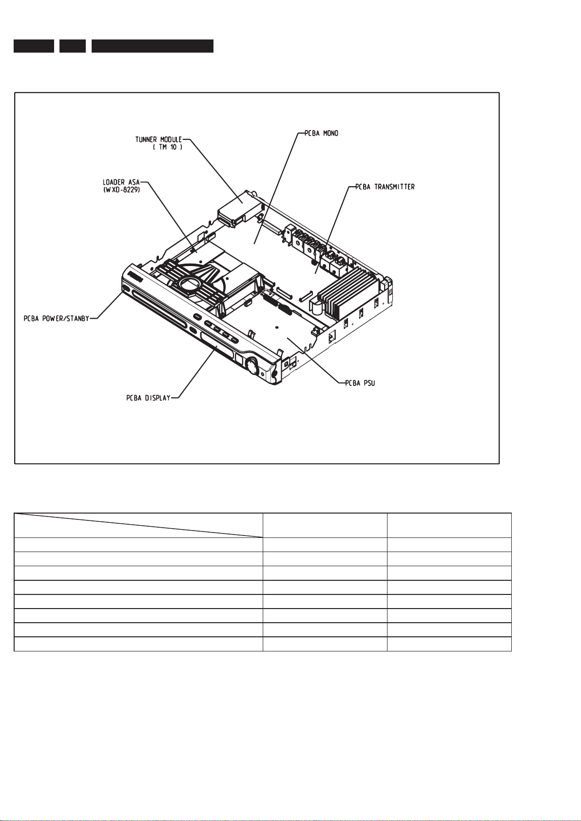
LOCATION OF PC BOARDS
HTS3500K/HTS5310K
HTS3300K & HTS3610k HTS3500K & HTS5310k
Video (Yellow, Cinch)
x x
Component Video Output, (Y/Pb/Pr)
x x
Digital In - Coaxial x x
TV In (Left/Right) x x
Auxiliary (Left/Right) x x
Line out (Audio) x
S-Video Output
x
Progessive Scan x
VERSION VARIATIONS:
Page 3

EN 3
3139 785 31640
Technical Specifications and Connection Facilities
1.
1. Specifications
1.1 General:
Mains voltage : 230V
Mains frequency : 50Hz
Power consumption : 100W
< 0.5W Eco standby
power
< 100W at 1/8 P
rated
(For main unit)
Dimension main unit : 360 x 54 x 324mm
1.2 Tuner
FM
Tuning range : 87.5-108MHz
Grid : 50kHz
IF frequency : 10.7MHz ± 25kHz
Aerial input : 75Ω coaxial
Sensitivity at 26dB S/N : < 7µV
Selectivity at 600kHz bandwidth : > 25dB
IF rejection : > 60dB
Image rejection : > 25dB
Distortion at RF=1mV, dev. 75kHz : < 3%
-3dB Limiting point : < 8µV
Crosstalk at RF=1mV, dev. 67.5kHz : > 28dB
Crosstalk at RF=1mV, dev. 40kHz : > 18dB
MW
Tuning range : 531-1602kHz
Grid : 9kHz
IF frequency : 450kHz ± 1kHz
Aerial input : Frame aerial
Sensitivity at 26dB S/N : < 4.0mV/M
Selectivity at 18kHz bandwidth : > 20dB
IF rejection : > 45dB
Image rejection : > 28dB
Distortion at RF=50mV, m=80% : < 5%
1.3 AMPLIFIER:
Output power
Front : 100W RMS / channel
Rear : 75W RMS / channel
Center : 100W RMS
Subwoofer : 150W RMS
Frequency response ±0.5dB : 20Hz-20kHz
Hum (Volume Minimum) : 200nW
Residual noise (Volume Minimum) : 40nW
Input sensitivity
Aux In : 1V ± 3dB at 22kΩ
Scart In : 1V ± 3dB at 22kΩ
Output sensitivity
Line Out (Left/Right) : 1V ± 2dB at 10kΩ
Scart Out (Left/Right) : 1V ± 2dB at 10kΩ
1.4 COMPACT DISC/VCD/DVD:
Video Decoding : MPEG-1/MPEG-2/
MPEG-4/DivX 3.11,
4.x & 5.x
Video DAC : 12 Bits
Signal System : PAL / NTSC
Video Format : 4:3 / 16:9
CVBS Out
1)
CVBS level : 1.0 ± 0.1V
p-p
Luminance S/N : >= 60dB
S-Video Out 1)
Y level : 1.0 ± 0.1V
p-p
Y S/N : >= 60dB
C level (burst) : 286mV pp +1/-4 dB
RGB/YUV Out 1)
Amplitude : 1.0 ± 0.1V
p-p
S/N : >= 60dB
1)
Output terminals to be terminated with 75Ω
Page 4
EN 4
3139 785 31640
2.
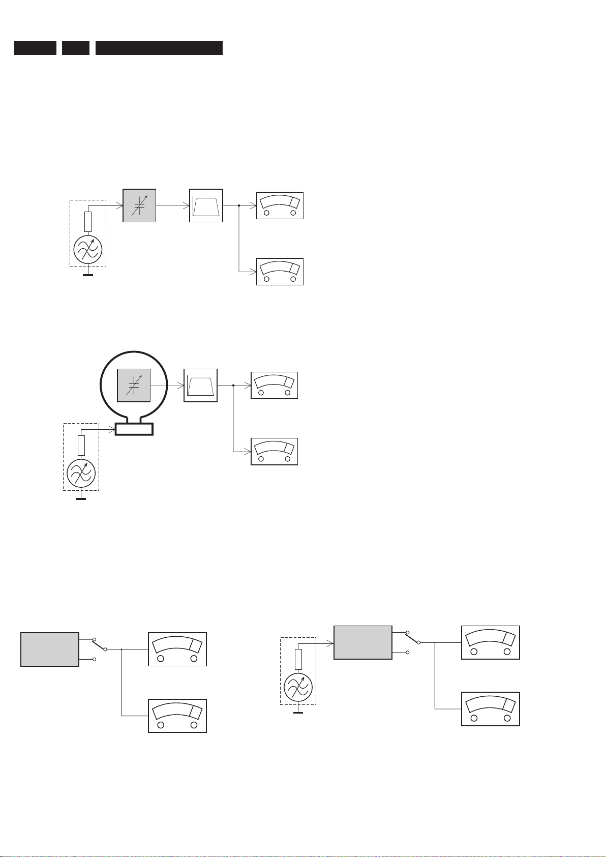
Measurements Setup, Service Aid & Lead Free Requirements
LF Generator
e.g. PM5110
Recorder
Use Universal Test Cassette CrO2 SBC419 4822 397 30069
LEVEL METER
e.g. Sennheiser UPM550
with FF-filter
S/N and distortion meter
e.g. Sound Technology ST1700B
L
R
DUT
or Universal Test Cassette
Fe SBC420 4822 397 30071
LEVEL METER
e.g. Sennheiser UPM550
with FF-filter
S/N and distortion meter
e.g. Sound Technology ST1700B
L
R
DUT
CD
Use Audio Signal Disc
(replaces test disc 3)
SBC429 4822 397 30184
Bandpass
250Hz-15kHz
e.g. 7122 707 48001
LF Voltmeter
e.g. PM2534
DUT
S/N and distortion meter
e.g. Sound Technology ST1700B
Frame aerial
e.g. 7122 707 89001
Tuner AM (MW,LW)
To avoid atmospheric interference all AM-measurements have to be carried out in a Faraday´s cage.
Use a bandpass filter (or at least a high pass filter with 250Hz) to eliminate hum (50Hz, 100Hz).
RF Generator
e.g. PM5326
Ri=50Ω
Bandpass
250Hz-15kHz
e.g. 7122 707 48001
LF Voltmeter
e.g. PM2534
DUT
RF Generator
e.g. PM5326
S/N and distortion meter
e.g. Sound Technology ST1700B
Use a bandpass filter to eliminate hum (50Hz, 100Hz) and disturbance from the pilottone (19kHz, 38kHz).
Ri=50Ω
Tuner FM
MEASUREMENT SETUP
2. Measurements Setup, Service Aid & Lead Free Requirements
Page 5
EN 5
3139 785 31640
Measurements Setup, Service Aid & Lead Free Requirements
2.
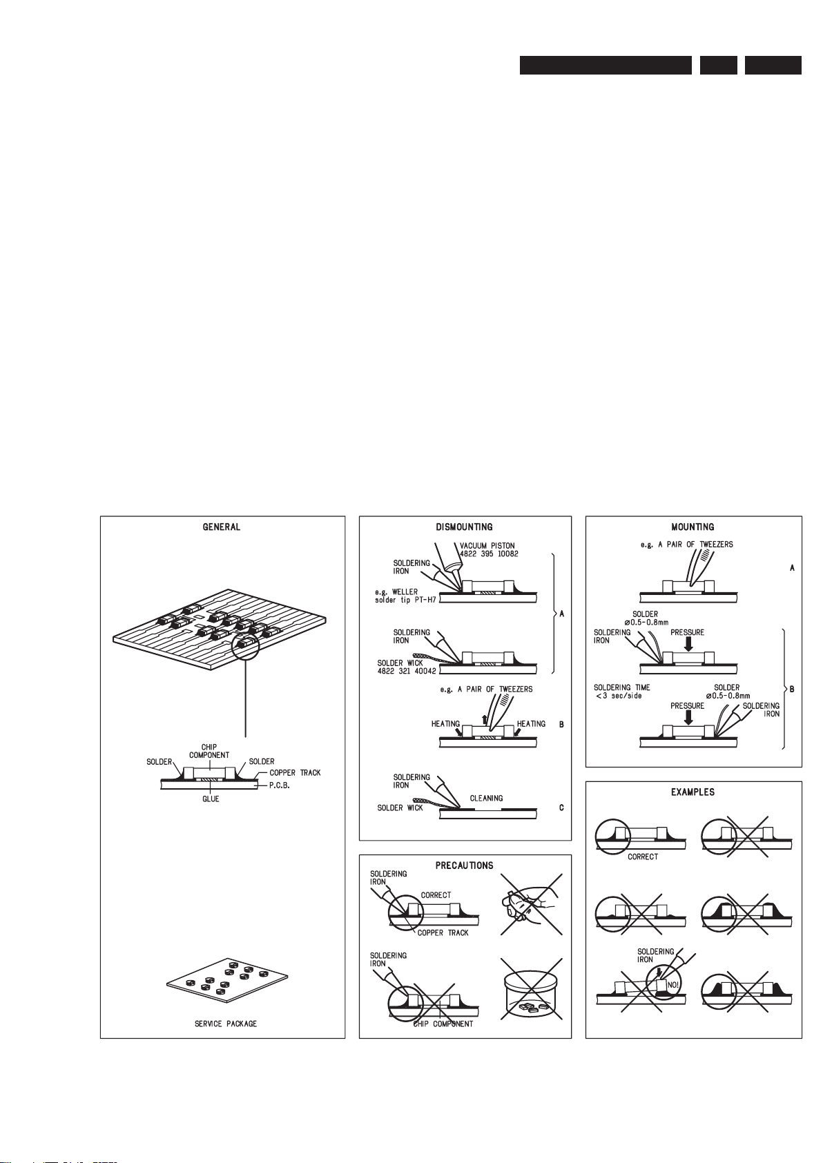
HANDLING CHIP COMPONENTS
SERVICE AIDS
Service Tools:
Universal Torx driver holder .................................. 4822 395 91019
Torx bit T10 150mm ............................................. 4822 395 50456
Torx driver set T6 - T20 ......................................... 4822 395 50145
Torx driver T10 extended ...................................... 4822 395 50423
Compact Disc:
SBC426/426A Test disc 5 + 5A ............................ 4822 397 30096
SBC442 Audio Burn-in Test disc 1kHz ................. 4822 397 30155
SBC429 Audio Signals disc .................................. 4822 397 30184
Dolby Pro-logic Test Disc ...................................... 4822 395 10216
Page 6

EN 6
3139 785 31640
2.
Measurements Setup, Service Aid & Lead Free Requirements
GB
WARNING
All ICs and many other semi-conductors are
susceptible to electrostatic discharges (ESD)
.
Careless handling during repair can reduce life
drastically.
When repairing, make sure that you are
connected with the same potential as the mass
of the set via a wrist wrap with resistance.
Keep components and tools also at thi
s
potential
.
F
ATTENTION
Tous les IC et beaucoup d’autres
semi-conducteurs sont sensibles au
x
décharges statiques (ESD).
Leur longévité pourrait être considérablement
écourtée par le fait qu’aucune précaution n’es
t
prise à leur manipulation
.
Lors de réparations, s’assurer de bien être relié
au même potentiel que la masse de l’appareil et
enfiler le bracelet serti d’une résistance de
sécurité
.
Veiller à ce que les composants ainsi que les
outils que l’on utilise soient également à ce
potentiel
.
ESD
D
WARNUNG
Alle ICs und viele andere Halbleiter sind
empfindlich gegenüber elektrostatischen
Entladungen (ESD).
Unsorgfältige Behandlung im Reparaturfall ka
n
die Lebensdauer drastisch reduzieren
.
Veranlassen Sie, dass Sie im Reparaturfall über
ein Pulsarmband mit Widerstand verbunde
n
sind mit dem gleichen Potential wie die Mass
e
des Gerätes
.
Bauteile und Hilfsmittel auch auf dieses gleich
e
Potential halten.
NL
WAARSCHUWING
Alle IC’s en vele andere halfgeleiders zi jn
gevoelig voor electrostatische ontladingen (ESD)
.
Onzorgvuldig behandelen tijdens reparatie ka
n
de levensduur drastisch doen verminderen.
Zorg ervoor dat u tijdens reparatie via een
polsband met weerstand verbonden bent me
t
hetzelfde potentiaal als de massa van het
apparaat
.
Houd componenten en hulpmiddelen ook op
ditzelfde potentiaal.
I
AVVERTIMENTO
Tutti IC e parecchi semi-conduttori sono
sensibili alle scariche statiche (ESD)
.
La loro longevità potrebbe essere fortemente
ridatta in caso di non osservazione della pi
ù
grande cauzione alla loro manipolazione.
Durante le riparazioni occorre quindi essere
collegato allo stesso potenziale che quello dell
a
massa dell’apparecchio tramite un braccialetto
a resistenza.
Assicurarsi che i componenti e anche gli utensil
i
con quali si lavora siano anche a questo
potenziale.
GB
ESD PROTECTION EQUIPMENT:
Complete Kit ESD3 (small tablemat, wristband,
connection box, extention cable and earth cable) ...........4822 310 10671
Wristband tester ....................................................................4822 344 13999
CLASS 1
LASER PRODUCT
GB
Warning !
Invisible laser radiation when open.
Avoid direct exposure to beam
.
S
Varning !
Osynlig laserstrålning när apparaten är öppnad och spärren
är urkopplad. Betrakta ej strålen
.
SF
Varoitus !
Avatussa laitteessa ja suojalukituksen ohitettaessa olet alttiina
näkymättömälle laserisäteilylle. Älä katso säteeseen
!
DK
Advarse !
Usynlig laserstråling ved åbning når sikkerhedsafbrydere er
ude af funktion. Undgå udsaettelse for stråling
.
F
"Pour votre sécurité, ces documents doivent être utilisés par
des spécialistes agréés, seuls habilités à réparer votr
e
appareil en panne"
.
GB
Safety regulations require that the set be restored to its original
condition and that parts which are identical with those specified,
be used
Safety components are marked by the symbol
!
.
NL
Veiligheidsbepalingen vereisen, dat het apparaat bij reparatie in
zijn oorspronkelijke toestand wordt teruggebracht en dat onderdelen
,
identiek aan de gespecificeerde, worden toegepast
.
De Veiligheidsonderdelen zijn aangeduid met het symbool
!
F
Les normes de sécurité exigent que l’appareil soit remis à l’état
d’origine et que soient utiliséés les piéces de rechange identiques
à celles spécifiées.
Less composants de sécurité sont marqués
!
D
Bei jeder Reparatur sind die geltenden Sicherheitsvorschriften zu
beachten. Der Original zustand des Geräts darf nicht verändert werden;
für Reparaturen sind Original-Ersatzteile zu verwenden
.
Sicherheitsbauteile sind durch das Symbol
!
markiert.
I
Le norme di sicurezza esigono che l’apparecchio venga rimesso
nelle condizioni originali e che siano utilizzati i pezzi di ricambi
o
identici a quelli specificati
.
Componenty di sicurezza sono marcati con
!
GB
After servicing and before returning set to customer perform a leakage
current measurement test from all exposed metal parts to earth ground to
assure no shock hazard exist. The leakage current must not exceed
0.5mA
.
Page 7

EN 7
3139 785 31640
Measurements Setup, Service Aid & Lead Free Requirements
2.
2.1 Lead Free Requirements
Pb(Lead) Free Solder
When soldering , be sure to use the pb free solder.
INDENTIFICATION:
Regardless of special logo (not always indicated)
one must treat all sets from 1 Jan 2005 onwards, according next
rules:
Important note: In fact also products of year 2004 must be treated in
this way as long as you avoid mixing solder-alloys (leaded/ lead-free).
So best to always use SAC305 and the higher temperatures belong
to this.
Due to lead-free technology some rules have to be respected by the
workshop during a repair:
• Use only lead-free solder alloy Philips SAC305 with order
code 0622 149 00106. If lead-free solder-paste is required,
please contact the manufacturer of your solder-equipment.
In general use of solder-paste within workshops should be
avoided because paste is not easy to store and to handle.
• Use only adequate solder tools applicable for lead-free solder
alloy. The solder tool must be able
o To reach at least a solder-temperature of 400°C,
o To stabilize the adjusted temperature at the solder-tip
o To exchange solder-tips for different applications.
• Adjust your solder tool so that a temperature around 360°C
– 380°C is reached and stabilized at the solder joint. Heatingtime of the solder-joint should not exceed ~ 4 sec. Avoid
temperatures above 400°C otherwise wear-out of tips will rise
drastically and flux-fluid will be destroyed. To avoid wear-out
of tips switch off un-used equipment, or reduce heat.
• Mix of lead-free solder alloy / parts with leaded solder alloy /
parts is possible but PHILIPS recommends strongly to avoid
mixed solder alloy types (leaded and lead-free).
If one cannot avoid or does not know whether product is leadfree, clean carefully the solder-joint from old solder alloy and
re-solder with new solder alloy (SAC305).
• Use only original spare-parts listed in the Service-Manuals.
Not listed standard-material (commodities) has to be
purchased at external companies.
• Special information for BGA-ICs:
- always use the 12nc-recognizable soldering temperature
profile of the specific BGA (for de-soldering always use the
lead-free temperature profile, in case of doubt)
- lead free BGA-ICs will be delivered in so-called ‘drypackaging’ (sealed pack including a silica gel pack) to protect
the IC against moisture. After opening, dependent of MSLlevel seen on indicator-label in the bag, the BGA-IC possibly
still has to be baked dry. (MSL=Moisture Sensitivity Level).
This will be communicated via AYS-website.
Do not re-use BGAs at all.
• For sets produced before 1.1.2005 (except products of 2004),
containing leaded solder-alloy and components, all needed
spare-parts will be available till the end of the service-period.
For repair of such sets nothing changes.
• On our website www.atyourservice.ce.Philips.com you find
more information to:
BGA-de-/soldering (+ baking instructions)
Heating-profiles of BGAs and other ICs used in
Philips-sets
You will find this and more technical information within the
“magazine”, chapter “workshop news”.
For additional questions please contact your local repair-helpdesk.
Page 8
EN 8
3139 785 31640
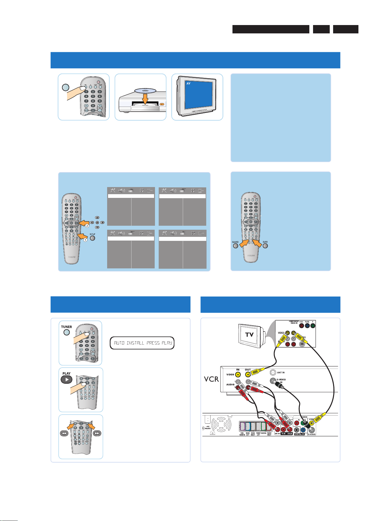
3.
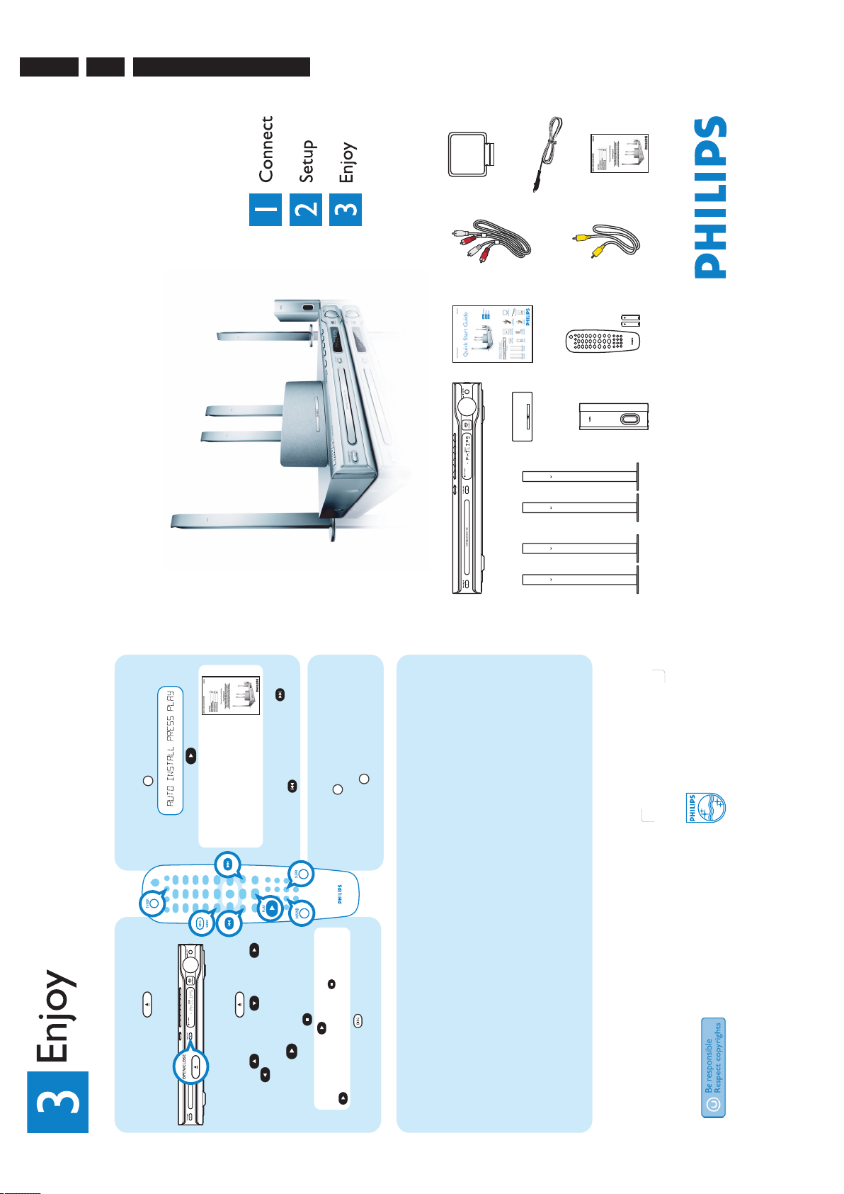
Directions For Use
QUICK START GUIDE
12nc: 3139 246 19191
HTS3500K
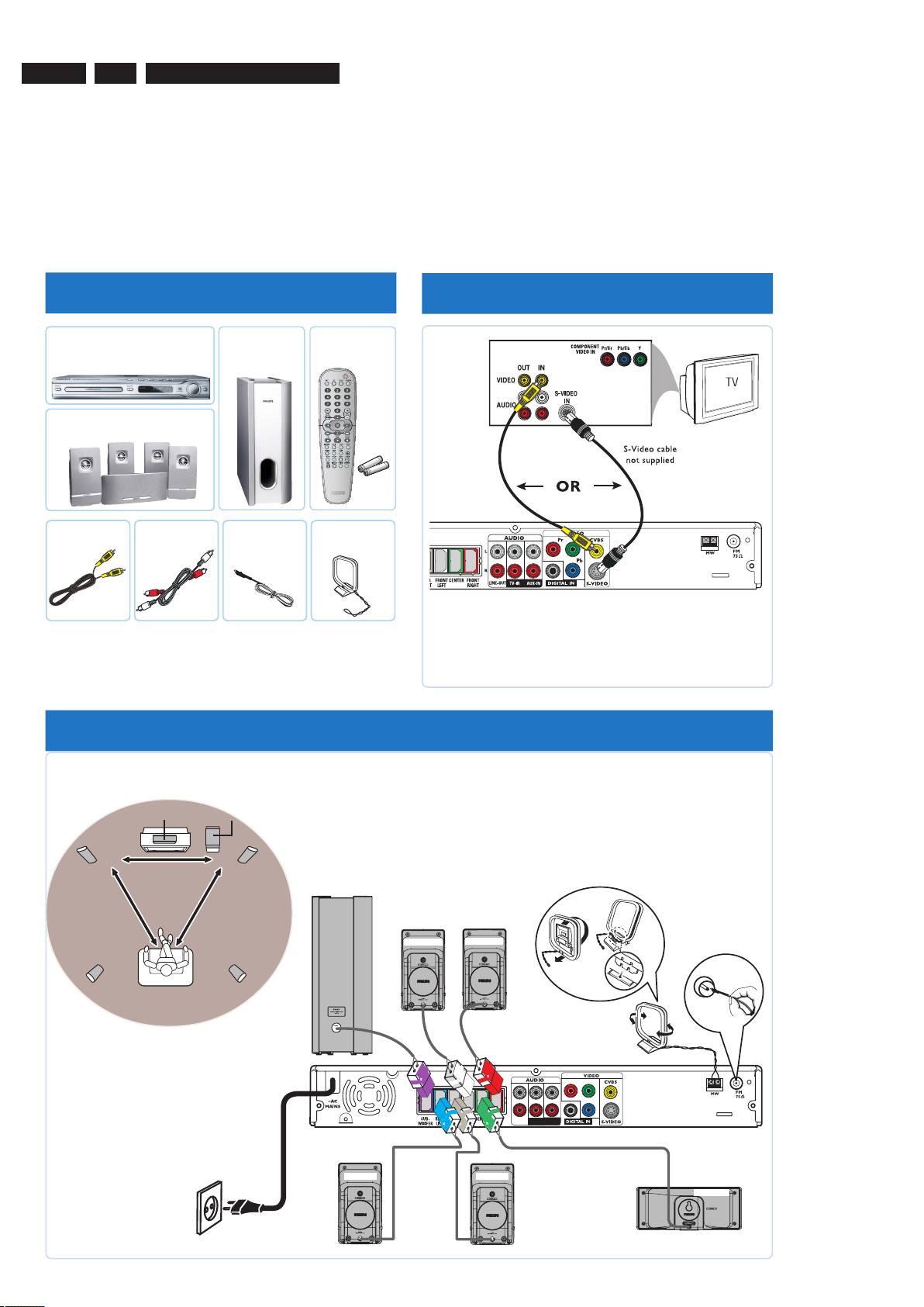
1 what’s in the box
2 connect TV
3 connect subwoofer, speakers and antennas
3a Placement of speakers
3c Connect the
FM and MW
antennas
REAR L
REAR R
FRONT L
CENTER
FRONT R
Subwoofer
TV
3b Connect the speakers
and subwoofer to the
DVD system
(refer to the user manual for
“Individual speaker volume
adjustment”)
3d Connect the mains
cord to the power
supply
L
R
Pb
Pr
Y
LINE OUT
TV IN AUX IN
�
REAR L
REAR R
CENTE R
FRONT L
FRONT R
Note: For connecting to a Progressive Scan TV,
refer to the user manual for proper
connections and detailed set up.
A
Remote control
includes 2x AA batteries
D
B
G H
C
Subwoofer
FM wire
antenna
MW loop
antenna
Main unit
Front/Rear/Center speakers
Video cable
E
Audio cable
F
A
H
G
E
A
3. Directions For Use
The following except of the Quick Use Guide serves as an introduction to the set.
The Complete Direction for the Use can be downloaded in different languages from the internet site of Philips Customer care Center:
www.p4c.philips.com
Page 9
EN 9
3139 785 31640
Directions For Use
3.
4 play a disc
DISC
4a Press DISC.
Point the remote control
towards the DVD system.
4b Load in a disc
Press OPEN CLOSE to
open and close the disc
tray.
4c Select correct
AV In channel
Switch to the correct
input source by using the
TV remote control.
GET PICTURE
•
Check the connection of the DVD system
to TV is in place (see 2 Connect TV).
• Check the AV mode on TV. It may be
called FRONT, A/V IN, or VIDEO. Choose
the different modes using TV remote
control.
• Or, use the TV remote control to select
Channel 1 on TV, then press Channel down
button until you get the picture.
• See your TV manual for more details.
A
udio Se
tup
P
age
S
p
eakers
V
olume
S
p
eakers
D
ela
y
N
ight
M
od
e
CD
U
psampling
V
ideo Se
tup
P
age
TV
T
ype
TV
D
ispla
y
P
rogressiv
e
P
ictur
e
S
etti
ng
P
reference
P
age
A
udio
S
ubtitl
e
D
isc
M
e
nu
P
arental
PBC
MP3/JPEG
N
a
v
P
asswor
d
D
i
v
X S
ubtitl
e
D
efaul
t
G
enera
l Se
tup
P
age
D
isc
L
o
ck
D
ispla
y
D
i
m
P
rogram
OSD L
a
nguag
e
S
cree
n
S
ave
r
DIVX(R) VOD
C
od
e
Refer to chapter “DVD Setup Menu Options” in the user manual
for detailed descriptions.
More settings and features
GET SOUND
To enhance the sound
quality
Press SOUND button to
select a predefined digital
sound effect.
Detailed playback features and additional
functions are described in the user manual.
No sound from rear
speakers?
Press SURR button to select
“Multi-Channel”.
5 programme radio stations
6 optional - connect VCR
IN-1 IN-2
NEEDS HELP? Visit our website www.philips.com/support
5a Press TUNER.
5b Press and hold PLAY 2
until “START ...” appears.
It will start to programme
all available radio stations.
5c Once complete, use
S / T to select a
preset radio station.
Note: This feature is only available
for first time setup.
Note: LINE OUT will output sound only when the speakers
volume are reduced to level 1 and below.
Page 10
EN 10
3139 785 31640
3.
Directions For Use
Quick Start Guide
HTS 5310K
What’s in the Box
Home Theatre System
Need help?
User Manual
For more product information refer to the user
manual of the home theatre system.
Online
Go to www.philips.com/support
2005 © Koninklijie Philips N.V.
All rights reserved.
12 NC 31 39 246 19181
www.philips.com
Troubleshooting
For more troubleshooting tips, see the user manual.
Problem Tip
No power • Check if the AC power cord is properly connected.
• Press the STANDBY-ON on the front of the DVD system to turn on the power.
No picture • Press DISC on remote control.
• Check connection to TV and ensure the plugs are firmly in place.
No sound or • Adjust the volume.
distorted sound • Check the speaker connections and settings.
• Check audio connections and press SOURCE button to select the correct input source.
Remote control • Check that the batteries are loaded correctly or replace the batteries with new ones.
does not work • Select the source (DISC or TUNER, for example) before pressing the function button.
• Reduce the distance between the remote control and the system.
• Point the remote control directly toward the IR sensor.
DVD system
Audio cables
(red & white plugs)
Video cables
(yellow plug)
Rear speakers
(left & right)
Listen to Radio
1 Press TUNER .
2 Press and hold PLAY until‘START’ appears.
Tip This feature is only availa-
ble for first time setup, refer
to user manual if you wish to
program radio stations again
or for manual programming.
3 Once completed you can use NEXT or
PREVIOUS to select a radio station.
Front display
Remote control
and 2 batteries
Quick start guide
Centre speaker
Subwoofer
Play DVD
1 Press OPEN/CLOSE on the front of
the DVD system to open the disc tray.
2 Place DVD in tray with the label facing up.
3 Press OPEN/CLOSE again.
4 Press UP , DOWN , RIGHT or
LEFT to scroll through the options in
the DVD menu.
5 Press PLAY on the option you want.
6 To stop press STOP .
Tip Press PLAY to resume from where
you stopped or press STOP and PLAY
to start from the beginning of the title.
7 Press DISC MENU to go back to the
DVD menu.
DVD Player (front)
Front speakers
(left & right)
Experience Surround Sound
1 Press SURR to switch between Stereo and
Multi-channel.
2 Press SOUND for either Concert, Drama,
Action or Sci-fi preset digital sound effects.
AM/MW
loop antenna
FM wire antenna
User manual
Page 11

EN 11
3139 785 31640
Directions For Use
3.
Connect Speakers &
Subwoofer to DVD System
Connect the various coloured plugs from the
speakers and subwoofer to the same colour
socket on the rear of DVD system.
Fix Antennas
1 Connect the FM antenna to the FM socket,
extend the antenna and fix it on the wall.
DVD System (back)
Pb
Pr
Y
2 Unfold the AM/ MW loop antenna and fix the
claw into the slot.
3 Push back tab and insert each wire into slot.
Position Speakers &
Subwoofer
1 Place centre speaker on or close to the TV.
2 Place subwoofer on the floor.
3 Place front speakers equal distance from the
TV and angle them 45 degree to the listener.
4 Place rear speakers facing the listener, equal
distance on the left and right.
Insert Batteries in
Remote Control
1 Remove batteries compartment cover.
2 Insert the provided batteries in the remote
control.Take note of where the positive and
negative ends should go.
3 Replace the batteries compartment cover.
Remote Control (back)
Find Correct Viewing Channel
1 Press STANDBY-ON on the DVD
system’s remote control.
2 Press DISC on the
remote control until ‘DISC’
appears on the front panel.
3 Switch on the TV.
4 Press ‘0’ on theTV’s remote
control, then repeatedly
press the Channel Down
button until you see the
DVD background screen.
This is the correct viewing
channel for the home
theatre system.
Tip For some TVs, to find the
correct viewing channel, you
can keep pressing the AV or
the SELECT buttons. If still
unable to find the correct
viewing channel, check the
connections again or check
your TV’s user manual.
Pb
Pr
Y
MW loop
antenna
DVD System (back)
Connect DVD system to TV
1 Use the yellow Video cable to connect the
yellow CVBS socket on the rear of the DVD
system and the yellowVIDEO IN jack at the
rear of the TV.
2 Plug in the power cable of the DVD system
to an AC outlet.
Tip To connect other devices
to the DVD system, refer to
the use manual.
T
o
an
t
e
n
n
a
or
s
et
-
to
p
b
o
x
Rear
Speaker
(left)
Rear
Speaker
(right)
Front
Speaker
(right)
Front
Speaker
(left)
Centre
Speaker
Pb
Pr
Y
DVD System (back)
Sub-Woofer
Connect Audio from TV
to DVD System (Optional)
Use the red & white audio cables to connect
the red & white TV-IN sockets on the rear of
the DVD system and the red & white AUDIO
OUT sockets on the TV.
DVD System (back)
Television (back)
Pb
Pr
Y
VIDEOOUT
(CVBS)
VIDEOOUT
(CVBS)
AUDIOOUT
AUDIOIN
Pb
Pr
Y
VIDEOIN
(CVBS)
VIDEO IN
(CVBS)
Pb
Y
DVD System (back)
Television (back)
Tip SomeTVs may not
have anAUDIO OUT jack.
Page 12
EN 12
3139 785 31640
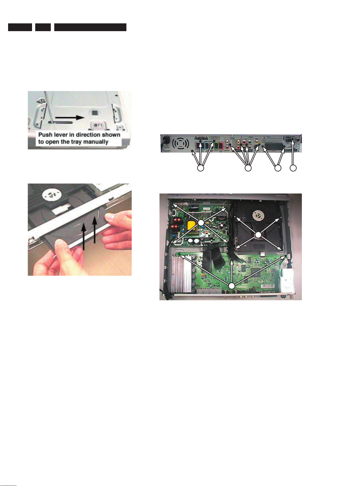
4.
Dismantling Instructions & Service Positions
B
B
B
Figure 4-3
A
D
Figure 4-4
C
E
4.2 Dismantling of the Tuner Module,
MONO Board, Front Board, PSU Module
1) Loosen 1 screw A (see Figure 4-3) to remove the Tuner
Module (pos 1040).
2) Loosen 9 screws B (see Figure 4-3) and 4 screws
(see Figure 3-4) to remove MONO Board.
3) Release 4 snap hooks to remove Front Board.
- 1 snap hook each on the left & right side (pos 161).
- 2 snap hooks on the bottom side (pos 161).
4) Loosen 4 screws E (see Figure 4-4) to remove the
PSU Module.
4. Dismantling Instructions
4.1 Dismantling of the DVD Loader
1) The tray can be manually open by inserting a minus
screw drive and push the lever in the direction as shown
in Figure 4-1 to unlock the tray before sliding it out.
Figure 4-1
2) Slide out the tray and remove the Cover Tray (pos 110)
as shown in Figure 4-2.
Figure 4-2
3) Loosen 5 screws to remove the Front Top.(pos 240)
- 1 screw each on the left & right side (pos 272)
- 3 screws behind
4) Loosen 4 screws C (see Figure 4-4) to remove the DVD
Loader.
Page 13

EN 13
3139 785 31640
4.
Dismantling Instructions & Service Positions
4.3 Service Positions
Mono Board
Thick Insulation Sheet
Front Board
Thick Insulation Sheet
PSU Board
DVD Loader
Page 14

EN 14
3139 785 31640
5.
Service Test Program
5. Service Test Program
TEST Activated with ACTION
EEPROM FORMAT
TEST
to Exit
Load default data. Display shows “NEW”.
Caution!
All presets from the customer will be lost!!
ROTARY
ENCODER TEST
Volume
Knob
Display shows value for 2 seconds.
Volume values increases or decreases in
steps of 1
until 0 (VOL MIN) or 40 (VOL MAX) is
reached.
LEAVE SERVICE
TEST PROGRAM
Disconnect
mains cord
LX8300SA & LX8320SA & LX8500W_Service Test Program_dd wk0429
To start service test program
open the tray with remote control
or front panel key, while plugging
in the mains cord press 2, 5 8 on
remote control, the tray will close
by itself and the set will display
shown “S-Vxx-yy”
Display shows
“SERVICE”
followed by ROM version
“S-Vxx-yy”
S refers to Service Mode
V refers to Version
xx refers to Software version number of BEA
(counting up from 01 to 99)
yy refers to Software version number of Front uP
(counting up from 01 to 99)
5.1 Display Test
Purpose:
This test is used to check the driving circuits, the display and whether there are
any short-circuits, open-circuits or any other defects.
Player:
Following display patterns are used to test the display and its connections to µP.
Pattern 1: Default: All display control pins are ON
- to check the open-circuits
Pattern 2: Alternate display control pins are on (Test Pattern: 0x55)
- to check the short-circuits on Data port
Receiver:
Following display patterns are used to test the display and its connections to µP.
Pattern 1: Default: All display control pins are ON
- to check the open-circuits
Pattern 2: Alternate display control pins are on (Test Pattern: 0x55)
- to check the short-circuits on Data port
key
"DisplayTest"
triggered?
n
y
A
ctivate and display
"Pattern1"
key
"DisplayTest"
triggered?
n
y
A
ctivate and display
"Pattern2"
Ma
in Menu
Display Test
key
" "
triggered?
n
y
Page 15

EN 15
3139 785 31640
5.
Service Test Program
5.1.1 Reprogramming of DVD version Matrix
After repair, the customer setting and region code may be lost.
Reprogramming will put the set back in the state in which it has left
the factory, ie. with the default setting and the allowed region code.
Model Region Region Code TV Type
HTS 3300K Russia 5 PAL
HTS 3500K Russia 5 PAL
HTS 5310K Russia 5 PAL
HTS 3610K Russia 5 PAL
To reprogram do as follows:
1) Power up the set and select DISC source.
2) Open tray by press “OPEN/CLOSE” button on the set or press
and hold “STOP” button on the RC.
3) Press the following buttons on the Remote Control:
<9> <9> <9> <9> <Zoom> <8> ......... for HTS 3500K/51
<9> <9> <9> <9> <
Zoom> <9> ......... for HTS 3300K/51
<9> <9> <9> <9> <Repeat> <0> ......... for HTS 5310K/51
<9> <9> <9> <9> <Repeat> <1> ......... for HTS 3610K/51
4) The display shows
‘YYYY-ZZ’ and the tray will close.
YYYY = model number (eg. 8300, 8500, etc.)
ZZ = slash stroke version (eg. 01, 69, etc.)
5.1.2 Procedure for check Software version
1) Power up the set and select DISC source.
2) Open tray by press “OPEN/CLOSE” button on the set or press
and hold “STOP” button on the RC.
3) Press “DISPLAY” button on the Remote control.
4) The TV screen will shows:
PPPP-Vxx YYYY-ZZ A BB
SERVO: GGGG GGGG REG:DD
PPPP = LX1S, LX1D or LX2W
xx = version number
YYYYY = model # 3300K/3500K/3610K/5310K
DD = region code
GGGG GGGG = version for servo code.
5.1.3 Burning of firmware
1. Unzip the zip-archive attached with this service information.
2. Start the CD burning software and create a new CD Project
(Data disc) with the following settings:
a. File System: ISO9660
b. Format: MODE 2/XA
c. Recording format: Single Session (Track at once),
Finalized CD
3. Place the content of the zip-archive into the root directory of the
new CD project.
4. Burn the data onto a blank CDR or CDRW.
Note: ISO9660 is mandatory, UDF discs are not supported!
The final CDROM must not contain any other data except
the file from the zip-archive.
5.1.4 Procedure to upgrade the firmware
1. Power up the set and open tray.
2. Insert the prepared Upgrade CDROM and close the tray.
3. The set will display:
LOAD -> MULTICH ->…………. ->UPG END.
The whole process takes less than 2 minutes.
Note: Do not press any button or interrupt the main supply upgrading
process,Otherwise the set may become defective.
4. When the upgrade is completed, the tray will close automatic.
5. The tray will close and the set will go to Standby mode
automatically when the upgrade process is completed.
5.1.5 Procedure to check the firmware version to confirm
upgrading
1. Power up the set and open tray.
2. Press the <Menu Display> button on the Remote Control.
3. The firmware version will be displayed on the top left hand corner
of the OSD.
5.1.6 Trade Mode
Trade mode is a feature that will block all set keys when enabled. It is
for dealers to prevent customers fromremoving disc, changing source
etc using the set keys.Rotary and Remote Control (RC) keys are still
allowed inTrade mode.
To activate Trade Mode:
1) Power up the set and select DISC source.
2) Open tray by press “OPEN/CLOSE” button on the set
or press and hold “STOP” button on the RC.
3) Then press buttons <2> <5> <9> on the RC.
4) The display shows
‘TRA ON’ and the tray will close.
Trade Mode is now enabled.
To deactivate Trade Mode:
1) Power up the set and select DISC source.
2) Open tray by press and hold “STOP”button on the RC.
3) Then press buttons <2> <5> <9> on the RC.
4) The display shows ‘TRA OFF’ and the tray will close.
Trade Mode is now disabled.
5.1.7 Procedure to change Tuner Grid (not for all versions)
1 Press SOURCE to select “FM” or “MW”.
2 Press STANDBY ON to switch the
DVD system to standby mode.
3 Press STANDBY ON again to turn on
the DVD system and hold down S
button on the front panel.
� The display will show "GRID 9" or
"GRID 10".
Helpful Hint:
– GRID 9 and GRID 10 indicate that the
tuning grid is in step of 9 kHz and 10 kHz
respectively.
Note: Repeating the same action will toggle back to its previous
tuning grid setting.
Page 16

EN 16
3139 785 316406.
FTD Display Pin Connection
6. FTD Display Pin Connection
Page 17

EN 17
3139 785 31640
7
Block Diagram, Wiring Diagram
AUX
IN
FTD DISPLAY
1702
VSTB 1
VSTA 2
VSCK 3
GND_MTK 4
40KHZ 5
IR 6
ioSTBY 7
8
9
VGL-1
-24V
+12VL
FRONT BOARD
3139 11335761
7400
TDA8922
7401
TDA8920
7402
TDA8922
Clock Generator
Curcuit
7301
HEF4013BT
CLOCK
OUT_1 OUT_2 OUT_3
OUT_4
OUT_5
OUT_6
Vdd Vdd Vdd
VGL-2
7701
IR
-V-FI L
(-17.8V)
+Vcc 1
+Vcc 2
+Vcc 3
AMP_GND 4
AMP_GND 5
AMP_GND 6
-Vcc 7
-Vcc 8
-Vcc 9
NC 10
CN2
CN1
SMPS04-01
Mitsumi
3139 117 11061
IC101
+5VL
T101
T102
IC151
VCC
D101 - D04
L100
LINE
OUT
CN3
SURR
RIGHT
1505
7708
V
63111
Controller / Driver
1711
Filament
DRIVER
40KHZ
1 +5VL
2 +12VL
3 GND_D
4 +5V EV
5 -24V
Drain
FB
GND
IC301
STBY ON/OFF
CN100
FUSE
STBY ON/OFF
POWER DOWN
Vss
Vss
Vss
1 +3V3
2
GND_D
3 +3V3
4 +5
VL
5 GND_D
6 +12VA
7 GND_A
8 -12VA
9 STBY ON/OFF
10 POWER DOWN
11 +12VL
12 GND
+5VD
STBY
1705
VOLB
VOLA
7900
1 +Vcc
2 +Vcc
3 +Vcc
4 AMP_GND
5 AMP_GND
6 AMP_GND
7 -Vcc
8 -Vcc
9 -Vcc
10 NC
VSS
Control
Circuit
C
S VIDEO
OUT
Y
1802A
SCART
RED
1800
CVBS
1802B
21
20
19
18
17
16
15
14
13
12
11
10
9
8
7
6
5
4
3
2
1
7201
IS42S16400A
DRAM
7109
MT1389B
DVD/SACD PLAYER SYSTEM CHIP
DVD LOADER
WXD-8136 ASA
3139 247 11121
SL+ 6
SL- 5
GND 4
LIMIT 3
SP+ 2
SP- 1
24P FLEX
1 GND_LD
2 DVD-LD
3 NC
4 HFM
5 MD
6 CD_LD
7 VD_DVD
8 VD_CD9
9 NC
10 E
11 VCC
12 VREF
13 GND
14 F
15 B
16 A
17 RF
18 CD_DVD SW
19 C
20 D
21 TRACK+
22 TRACK-
23 FOC+
24 FOC-
1101
GND_LD 1
DVD-LD 2
NC 3
HFM 4
MD 5
CD_LD 6
VD_DVD 7
VD_CD 8
NC 9
E 10
VCC 11
VREF 12
GND 13
F 14
B 15
A 16
RF 17
CD_DVD SW 18
C 19
D 20
TRACK+ 21
TRACK- 22
FOC+ 23
FOC- 24
7203
M29W160ET70
FLASH
+5M
+L_V33
+L_V33
7110
MM1646XH
Motor Drivers
LOAD+ 1
LOAD- 2
TROUT 3
GND 4
TRIN 5
1105
7200
IM24C16-RDW6
NVRAM
1109
1401
5130
27MHZ
7202
CS8415A
Digital Audio Interface
receiver
1502
SP- 1
SP+ 2
LIMIT 3
GND 4
SL+ 5
SL- 6
LOAD- 1
LOAD+ 2
TROUT 3
GND 4
TRIN 5
1102
AM / FM
Tuner TM10
2422 542 00014
AM
FM
GND 1
NC 2
SD 3
+9.1V 4
RDS_Mux
5
Rch 6
CE 7
Lch 8
Data_IN 9
DO/Stereo
10
CL 11
1 GND
2 NC
3 TU_SD
4 +9V
5 TU_RDS_IN
6 TU_RIGHT
7 TU_CE
8 TU_LEFT
9 TU_DAT_IN
10 TU_DO_STEREO
11
TU_CLK
1 +3V3_D
2
RXD
3 TXD
4 GND
1108
1 VSTB
2 VSDA
3 VSCK
4 GND
5 PCM_LRCK
6 RC6
7 IO
STBY
8
9
1501
AUX IN
Logic Switch
LO_Left
LO_Right
SCART_TV_L_IN
Left_in
Right_in
7503
74HC4052
Input Switch
7615
CS42406
CODEC
Left_in
Right_in
TV IN
MIC IN
Tuner IN
SEL-B
SEL-A
LPF Circuit
7613/7616/
7621
RDS_DA
RDS_CLK
6 channel audio data
Mode 12
Mode 34
Mode 56
STANDBY
BOARD
Standb
y
Button
1 stby
2
1 +5VAM
2 MIC
3 MGND
4 -12VAM
1 +5VAM
2 MIC
3 MGND
4 -12VAM
Mute
Circuit
RDS_CK
RDS_DA
Video
FRONT
LEFT
FRONT
RIGHT
CENTER
SUB_
WOOFER
SURR
LEFT
+3V3 1
GND_D 2
+3V3 3
+5VL 4
GND_D 5
+12VL 6
GND_A 7
+12VA 8
POW_ON 9
POWER_DN 10
+12VL 11
GND 12
TV IN
CVBS
7662
SAA6581T
RDS IC
1500
Component
Video
Digital In
1806
+5VL 1
+12VL 2
GND_D 3
+5VSTBY 4
-24V 5
1703
1707
1708
1900
1900
1302
VDD
Mono BOARD
MPEG+AV+AMP
3139 11331471
7. Block Diagram
HTS 3500 block diagram.pdf_051305
Page 18

EN 18
3139 785 31640
7.
Block Diagram, Wiring Diagram
SCART
S-V
CVBS
YPbPr
Spdif
AUX_in
TV_in
L_out
SUB
SL
SR
FLCFR
1800 1802 1806 1502 1501 1401 1400
2P EH TO FAN
Mono board( AV+MPEG+AMP)
10P EH TO PSU
1500 1302
+12VA 1 +Vdd
MIC +Vdd
GND +Vdd
-12Va GND_AMP
GND_AMP
4P GND_AMP
-Vss
-Vss
-Vss
10 NC
+3V3
GND
+3V3
+5VL
GND
+12VA
GNDA
-12VA
STBY
POWER_DN
+12VL
GND
1 12
1900
12P EH TO PSU
313911103771(MIS 12P/140mm) 313911101771(MIS 10P/140mm)
+3V3
GND
+3V3
+5VL
GND
+12VA
GNDA
-12VA
STBY
POWER_DN
+12VL
GND
+Vdd
+Vdd
+Vdd
GND-AMP
GND_AMP
GND_AMP
-Vss
-Vss
-Vss
NC
1 12 1 10
12P EH TO MONO 10P EH TO MONO
PSU
1 +5VL
DVD loader +12VL
GND
+5V EV
5 -24V
5P EH TO Front
313911101901 ( MIS 09/340/09 OE)
+5VL
+12VL
GND
+5V EV
-24V
VSTB
VSTA
VSCK
GND
41K
RC6
STBYNCNC
1 9
1 5 9P EH BOARD INTO MONO
Front +MIC
3139 113 35771 3139 113 35761 FR1 2-layer
2P-stand-by switch 313911104521 (MIS 04/480/04 OE)
8701 313911103311 (MIS 02/220/02 OE)
313911103541(MIS 05/1
8
3139 243 31471 141X382 FR4 2-layer
+12VA
MIC
GND
-12A
4P EH TO mono( MIC)
Port-s
TU_SCL
TU_SDA
TU_SD
TU_L
TU_Stereo
TU_R
NC/RDS
+9V
GND
LOAD-
LOAD+
TROUTGND
TRIN
SP-
SP+
LIMIT
GND
SL+
SL-
24P FFC TO OPU
5P PH SERVO
6P PH SERVO
DVD LOADER
VSTB
VSTA
VSCK
GND
LRCLKRC6
STBYNCNC
1105
9P EH TO FRONT
6P/180mm PH
1102
1103
1505
24P/140mm FFC
5P/220mm PH
11P FFC TO TUNER
1101
Port-s
TU_SCL
TU_SDA
TU_SD
TU_L
TU_Stereo
TU_R
NC/RDS
+9V
GND
8001 313911103781(FFC FOIL 10P/120/10P AD FOLD)
TUNER
TM10
Wiring Diagram
HTS 3500-3300 wiring diagram.pdf _051305
Page 19

EN 19
3139 785 31640
8
5
DIN
DOUT
STB
CLK
OS
C
1
2
KEY
SW
I
LED
SEG<1:20>
KS
GRID
4
6
8
7
VSS
5
4
3
2
1
3
4
1
2
3
4
IC
1
2
3
4
5
VE
E
2
VD
D
3
1
11
10
9
8
7
6
12
13
14
15
16
12
11
10
9
2700 C3
2701 C3
2702 B4
2703 B4
2704 C5
DRAOBONOM
F711 F2
F712 G2
F713 G2
F714 G2
F715 D9
F716 C8
F717 C1
1
F718 B2
F719 B2
F720 C2
F721 D1
F723 D1
F724 D1
H
I
F708 F2
F709 F2
3735 I12
3736 I12
3737 I1
3
3738 I1
3
F701 E2
F702 E2
F703 E2
F704 E2
F705 E2
F706 F2
5 6 7 8 9 10 11 12 13
1 2 3
4
1714 H5
1715 H6
1716 H7
1717 G8
F734 C4
F735 D1
6716 G6
IR
F710 F2
FO 5011
M
ORF/OT
32
-24V
B
1
C
D
E
F
G
D
E
F
G
H
I
A
FROM 1500 OF MONOBOARD
F707 F2
3701 B2
2717 E2
2716 E2
4
+5V_Ever
2718 H2
2719 G8
A
B
C
2711 D10
2712 E8
2713 E8
2714 E8
2715 I1
3
6717 G6
6718 H8
6719 H8
6720 I8
7701 I2
7702-1 B4
7702-2 B6
7703 C3
7704 E5
7705 I1
2
7706 I1
2
7707 I1
2
7708 E1
0
1708 G7
1709 B1
13
5 6 7 8 9 10 11 12
3704 C4
3706 C5
ioSTBY
3705 B5
3702 B2
3703 C4
1710 H5
1711 H6
1712 H7
1713 H7
2726 D1
0
2729 I8
3700 C2
F726 H3
F727 I2
F728 I4
F729 D8
F730 E10
F731 E10
F732 F9
F733 G9
6712 G12
6715 G13
+12VL
6709 G12
6706 G11
6707 G11
FROM 0202 OF PSU
6705 G11
6708 G12
6710 G12
6704 E1
0
3723 E4
3724 H2
3725 I3
6700 E5
6701 D9
6702 D8
6703 C4
1701 C8
1702 F2
1703 E1
1705 G3
1707 D1
3732 F8
VSCK
3733 I1
0
VOLB
3731 I7
3734 I1
1
2720 G8
2721 I1
0
2722 I1
1
2723 H1
1
2724 E1
0
2725 E4
3726 I4
3727 I4
3728 I5
3729 I6
3730 I6
DISPLAY BOARD
6711 G12
+5VL
GND_MTK
40kHZ
6713 G1
3
6714 G1
3
4701 G9
4702 G9
4703 G4
4704 G4
5700 B3
F725 E5
3721 E4
2705 C4
2706 C5
2707 C5
2708 B5
2709 C6
2710 E8
3714 D8
3715 E9
3716 F6
3717 F7
3718 F7
3719 E5
3720 E5
3746 D8
3745 E4
VSDA
4700 G9
3744 H9
VSTB
3707 C6
3708 B6
3709 D4
3710 C8
3711 C1
1
3712 C8
3713 C1
1
3739 C7
3740 D3
3741 G4
3742 G5
3743 H9
VOLA
3722 E5
GND_D
F704
613SAB4176
F710
0172
2u2
9
1
72
p001
F711
7705
BC817-25
F709
3
B
2
C
4
5
EVEMC
1705
1
A
3734
2K2
9373
0
K1
0073
K01
613SAB0176
33R
3710
9K3
6
07
3
SKQNAB
1711
BC847B
7704
6700
LTL-816EELC
BC857B
7706
7176
613
S
A
B
613
S
A
B8
076
5072
0
u
1
613
S
AB
6
076
613SAB5076
3723
4K7
8K2
3709
330R
F724
2172
3735
MGND
p01
613SAB9076
MGND
13
73
7K
4
3711
33R
n001
1172
3724
100R
52
7
3
K0
1
3
4
7K4
827
3
1707
WH04D-1
1
2
1
2
3
4
5
6
7
8
9
WH09D-1
1702
SKQNA
B
1712
p22
5172
8072
p0
0
1
SKQNAB
1716
2709
47p
MGND
R051
0473
5700
22u
p001
92
72
n
0
0
1
8
172
F726
613SAB7076
33R
3713
7K
4
44
7
3
34
73
7K
4
470n
2702
3172
p01
3712
33R
3705
2K7
2
GND
4
5
1
OUT
3
VS
TSOP4836ZC1
7701
3727
1K2
SKQNAB
1714
F734
F732
F733
F730
F731
u0
1
F707
V
53
1272
7373
F706
7K4
7
K4
1
47
3
7703
BC847B
BAS31
6
6719
613SAB
2076
n33
3272
7
07
2
1K0
3726
0u
1
MGND
6K8
3707
F703
1713
SKQNA
B
MGND
MGND
F727
F728
1717
455K
WH05D-1
1703
1
2
3
4
5
MGND
7
K4
037
3
61
3
SAB
1
176
F701
2703
470n
F716
p0
0
1
1
0
7
2
F715
F702
F735
BAS316
6704
BC847B
7707
SKQNA
B
1715
5
173
F712
K
0
1
8373
K01
3746
1R0
1
2
3
4
413354
4
3
15
15
36
16
17
18
19
20
21
22
23
9
24
25
26
27
28
29
30
31
32
35
7
10
11
12
13
50
49
48
47
46
52
8
6
5
44
43
42
41
40
39
38
37
DRIVER
CONTROLLER
/
FIP
Φ
UPD16311GC-AB6
7708
n001
617
2
p01
4172
2724 10u
p00
1
0272
0u1
60
72
2
2
8P
12
9P
F729
6
1P
41
31
71P
2P
82
72
3
P
62
4P
5
2
5P
42
6P
3
2
7P
232F9
2
1P
02
01P
91
11P
2
1
P
8171
31P
41P
6
1
51P
51
5G26
G3
G4
7
8G59
G6
01
G
7
1
1
G8
1
1F
DSP
HUV-08SS57T
1701
4
G1
R
0
74
9173
100n2726
F720
SKQNA
B
1710
5
MSJ-035-11C B AG SR
1709 1
2
4
BAS316
6718
MGND
4
072
p7
4
2K2
3733
WH02D-
1
1708
1
2
7173
3K3
7702-1
3
2
1
84
1K0
3704
LM833D
613SAB2176
0
0
72
p
0
0
1
8
173
3K3
MGND
BAS31
6
3K3
6173
6720
1076
B
2
.6
ZD
P
F717
F705
4K7
3720
613SAB5176
6373
R033
1K2
3701
F708
F721
2
47
3
7
K
4
F719
F714
F718
4701
1273
7K4
7172
84
n001
7702-2
LM833D
5
6
7
DNG
M
F723
K86
30
73
2K2
3702
K22
4173
4703
4704
BAS316
6703
1M0
3732
MGND
1K0
3708
6176
613
S
AB
MGND
10u
2722
F713
35V
92
7
3
7K
4
2273
R074
5272
0u
1
F725
4K7
3745
4702
613SAB3176
4700
)3(P
)2(P
)71(P
)61(P
)51(P
)41(P
)
31(
P
)2
1
(P
)
11(
P
)01(P
)1(P
)8(G
)7(G
)
6(G
)5
(
G
)
4
(
G
)3(G
)
2
(
G
)
1(G
-12VAM
+5VAM
VOLA
V42-
+5VL
+5VDSTBY
stdby_2
+5VDSTBY
stdby_1
VOLB
)9(P
)8
(
P
)
7
(P
)6(P
)
5(P
)
4(P
+5VDSTBY
+5VDSTBY
G(7) G(6)
G(5) G(4) G(3)
P(1)
MISCB
MISCA
MISCB
+5VDSTBY
P(3)
P(3) P(2)
P(2)
VOLA
VOLB
+5VDSTBY
REMOTE
RESE
T
P(1)
P(1)
+12VL
-12VAM
+5VAM
MIC_DET
-V_FIL
VGL+
1
+12VL
VGL+
1
40kH
Z
+5VDSTBY
REMOTE
VGL-1
P(10
)
P(11
)
P(12
)
P(13
)
P(14
)
MGND
+5VAM
MIC
+5VAM
-12VAM
MIC
MIC_DET
MISCA
stdby_1
+5VDSTBY
40kH
Z
stdby_2
-24V
VGL-1
RESE
T
-V_FIL
G(1)
G(2)
G(8)
P(15
)
P(16
)
P(17
)
P(2)
P(3)
P(4)
P(5)
P(6)
P(7)
P(8)
P(9)
3139_113_35766_a2_sh130_sh1.pdf 2005-05-18
8. Front: Display
Circuit Diagram and PWB Layout
Page 20

EN 20
3139 785 31640
8.
Front: Display (topview)
Topview_DisplayBd_35766.pdf 2005-11-02
Circuit Diagram and PWB Layout
Page 21

EN 21
3139 785 31640
Front: Display (Bottom view)
8
Circuit Diagram and PWB Layout
BottomView_DisplayBd_35766.pdf 2005-11-02
Page 22

EN 22
3139 785 31640
Front: Standby
1901 A1
1 2
1 2
A
B
A
B
1900 A1
F901 A1
2901 B1
2902 B1
F902 A1
p
0
2
2
1092
SKQNAB
1901
1
2
B2B-EH-A
1900
F902
F901
p
0222092
3139_113_35776_a4_sh130_sh1.pdf 2005-05-18
8.
Circuit Diagram and PWB Layout
TopView_StandbyBd_35776.pdf 2005-11-02
BottomView_StandbyBd_35776.pdf 2005-11-02
Front: Standby (topview)
Front: Standby (Bottom view)
Page 23

EN 23
3139 785 31640
Mono Board: Circuit Diagram (Part 1)
COM
OUTIN
VIN3
VIN4
VINLOp
VINLOn
D
NGERP
CC
V
R
W
P
CCVER
P
PS
VBIAS
SB
VIN1
VIN2p
VIN2n
DNGRWP
DNG_SH
OUTLn
OUTL
p
OUT4
n
OUT4
p
OUT3
n
OUT3
p
OUT2
n
OUT2
p
OUT1
n
OUT1
p
VO2
T179 C3
T181 C4
T182 C4
T183 C5
T184 D4
T185 D5
T186 F5
T187 F5
T138 B9
T148 I9
T149 I9
T150 I9
T151 I9
T188 F5
T189 F5
T190 A6
T191 I1
1
T173 A4
T174 B2
T175 B3
T176 B5
T164 C13
T165 C1
3
T166 C1
3
T167 C1
3
T168 D1
3
T169 D1
3
T171 A2
T172 A3
T118 E2
T119 E1
T120 E2
T121 E1
T177 B5
T130 G1
T131 H1
T132 H1
T133 I1
T134 I1
T135 I1
T136 E6
T137 E7
T103 D1
T104 D2
T105 D1
T106 D2
T152 I9
T153 I1
0
T154 I10
T155 I1
0
T156 I1
0
T157 I10
T158 I1
0
T159 C1
3
T160 C1
3
T161 C1
3
T162 C1
3
T163 C13
T110 E2
T111 E1
T112 E2
T113 E1
T114 E2
T115 E1
T116 E2
T117 E1
5125 D3
5126 E5
6100 I1
0
7102 A2
T122 E2
T123 F1
T124 F1
T125 G1
T126 G1
T127 G1
T128 G1
T129 G1
7112 I1
2
F125 F1
2
F126 F1
2
F141 C6
F155 E6
F156 E6
T101 D1
T102 D2
4109 H10
5101 A8
5104 A1
5105 A2
T107 D1
T109 E1
5116 B9
5117 B1
5118 B3
5119 B4
5120 B5
5122 C2
5123 D2
5124 D4
3181 I9
3182 I9
3183 I9
3184 I9
7104 D4
7105 D3
7106 E2
7107 E3
7108 E3
7109 E9
7110 F3
7111 H12
4101 B1
0
4102 C6
4103 C6
4104 C6
4105 D6
4106 D6
4107 F6
4108 F6
3159 H5
3160 I2
3161 H1
1
3162 I2
5106 A3
5107 A4
5108 A6
5113 B7
5114 B8
5115 B9
3173 D2
3174 D2
3175 A10
3176 A10
3177 A12
3178 A12
3179 A12
3180 B12
3141 G5
3142 G5
3143 G2
3144 G5
3121 = 1K8 for high Z mode
3185 C12
3186 D12
4100 B9
3151 H9
3152 H9
3153 H10
3154 H10
3155 H10
3156 H10
3157 H10
3158 H5
3124 E12
3125 D13
3126 D4
3127 D12
3164 I9
3165 I9
3168 I2
3169 I2
3170 I1
1
3171 I1
1
3172 I1
1
3133 E2
3134 E3
3135 E2
3136 E5
3137 E5
3138 F6
3139 F6
3140 G4
3105 A12
3106 A9
3107 B10
3108 A7
3145 G1
3146 G5
3147 H1
3148 H2
3149 H2
3150 H5
3114 B1
3
3115 A1
1
3116 B1
2
3118 B9
3119 B7
3120 B11
3121 C1
2
3123 D12
2220 E6
2221 E5
2222 F6
2223 G4
3128 D3
3129 D2
3130 D13
3131 D1
2
3132 E3
2246 I9
2249 I1
1
2250 I1
0
2251 I1
1
3101 A1
2
3102 A13
3103 A6
3104 A12
2205 C6
2206 C6
2207 C6
2208 D2
3109 A10
3110 B1
2
3111 A10
3112 B1
2
3113 A1
0
2212 E2
2213 E5
2214 E2
2215 E5
2216 H5
2217 E5
2218 I2
2219 I2
2179 G5
2180 E3
2181 G2
2182 G2
2224 F6
2241 I8
2242 I8
2243 I8
2245 I9
2197 G6
2198 H5
2199 H2
2200 C12
2201 C6
2202 C6
2203 C1
2
2204 C6
2155 B6
2156 B6
2157 B6
2158 B9
2209 D2
2210 D5
2211 D3
2168 C3
2169 C4
2170 C4
2171 C4
2172 C4
2173 C4
2174 C5
2175 B10
2137 B13
2138 B1
2139 B2
2140 B2
2183 H2
2184 H1
2185 H2
2186 H2
2187 I8
2188 I9
2194 G5
2195 G5
2196 G5
2147 B4
2148 B4
2149 B5
2150 I1
2
2151 B5
2152 B6
2153 B6
2154 B6
2119 A5
2120 A6
2121 A8
2122 A10
NB :
2159 B7
2160 B7
2161 B8
2162 B8
2163 B8
2164 B8
2165 I5
2166 I5
2167 C2
2129 B8
2130 B8
2131 B8
2132 B9
2133 B9
2134 A10
2135 A11
2136 B12
I
A
B
C
2141 B3
2142 B3
2143 B3
2144 B3
2145 B3
2146 B3
2111 A3
2112 A4
2113 D1
3
2114 H7
2115 A4
2116 H7
2117 A8
2118 A8
13
1 2
3
2123 A10
2124 B12
2125 B12
2126 D13
2127 B7
2128 B7
A
B
C
D
E
F
G
H
D
E
F
G
H
I
1101 D1
1102 G1
1103 H1
1105 I9
2104 A12
2105 A12
2106 A13
2107 A7
2108 A8
2109 A9
5 6 7 8 9 10 11 12
T192 D4
T193 E3
T194 I1
1
T195 I1
0
4 5 6 7 8 9 10 11 12 13
NB
1107 F5
1108 I1
0
1109 H1
1110 C1
3
2100 A3
2101 A3
2102 A8
2103 A12
1 2 3 4
T167
R00
12
813
#
D
RU
6
9
7
9
2_81DDVD
8
9
2_
1
PU
9
9
3_
1
PU
T186
12AOI
9
8
MB
9
EL
A
09
7D
A
1
9
71A
2
9
0AOI
39
3_S
S
VD
4
9
#
RWU
5
9
0D
A
1
8
1DA
2
8
2
DA
3
8
3
DA
4
8
2
_
S
S
VD
58
4
DA
6
8
5
DA
78
6D
A
8
8
2
AHG
IH
4
7
1
A
H
G
IH
5
7
6
7
02AOI
77
#SCOI
8
7
1AOI
#EOOI
97
8
MA
2_3
D
DV
D
0
8
61A
7
6
7AHGIH
8
696
6AHGI
H
7
DVDRFIN
0
7
5AHGIH
17
4
AHGI
H
27
3AHGIH
3
7
1_3DDVD
DVDRFIP
60
IOA18
61
IOA19
62
DVSS_1
63
APLLCAP
APLLVSS
64
5
6
3DDVLLPA
6
6
#
R
WOI
52
53
IOA2
54
IOA3
55
IOA4
56
IOA5
57
IOA6
58
IOA7
59
HIGHA0
6
45
46
USB_VDD3
FG
47
TDI
48
TM
S
49
5
DVD
D
TCK
50
51
TDO
DVDD18_1
38
39
TROPENPWM
4
DVD
C
PWMOUT1
40
TRO
41
FOO
42
USB_VSS
43
44
USBP
USBM
30
31
FEO
TEO
32
TEZISL
V
33
OP_OUT
34
OP_INN
35
OP_IN
P
36
37
DM
O
FMO
CGFR
FERI
5
5
2
652
3DDVA
RFLVL
26
SGND
27
V2REFO
28
V2
0
29
3
DVDB
VREFO
CZFR
H
842
PLP
T
RC
942
DNGFR
CSO
25
PQ
E
C
052
NQEC
1
52
P
S
O
2523
52
NSO
4
52
MCV_
S
042
14
2
S
S
VC
D
A
24
2
PFERV_S
3
42
N
F
ER
V
_S
3
D
DVF
R
44
2
CD
P
RFR
542
642
CAPR
F
R
742
S
SV
LLP
332
P
L
�ECA
D
I
432
3DDVLLP
NOFPL
532
PIFPL
632
NIFPL
732
8
3
2
POFP
L
9
3
2
3DDVCDA
SVDD3
24
FIDPS
8
1DNGF
R
622
7
2
2
81DDVFR
O
L
ATX
822
IL
A
TX
9
22
LDO1
23
03
2
OFTIJ
1
32
NFTIJ
2
32
912
2
ATADSA
22
LDO2
3ATADSA
0
2
2
6_8
1
DD
V
D
122
4ATA
D
S
A
222
32
2
31_
S
SVD
422
AT
A
D_CM
522
1
1
2
KCBPS
212
01_3DDVD
KCRLA
312
KCBA
412
51
2
KLCA
6
1
2
21_SSVD
712
0ATADSA
1ATADSA
8
1
2
402
9_3DDVD
502
NYSV
602
7VUY
702
NY
S
H
802
K
L
CMPS
9
02
AT
ADPS
21
MDI2
KCR
L
PS
012
BSSVCAD
3VUY
891
991
ADDVCAD
2
DVD
A
MDI1
20
4VUY
002
ASSVCAD
102
202
5VUY
6VUY
302
190
VREF
FS
191
192
YUV0
CSSVCAD
391
1VUY
491
591
BDDVCAD
691
2VUY
791
RD21
184
RD20
185
RD19
186
RD18
187
RD17
188
RD16
189
DACVDD
C
TPI
19
176
RD24
177
DQM
3
178
DQM
2
179
TNI
18
RD23
180
181
RD22
DVDD3_8
182
183
RD30
169
CDFO
P
17
RD29
170
RD28
171
RD27
172
DVDD18_5
173
RD26
174
DVSS_11
175
RD25
161
RA
7
162
DVSS_10
163
164
RA
6
RA
5
165
RA
4
166
167
DVDD3_7
RD31
168
154
155
DVDD3_6
156
RCLK
CK
E
157
158
RA11
159
RA
9
16
CDFO
N
160
RA
8
DVSS_
9
147
148
DVSS_
8
RA
1
149
15
SD
150
RA
2
151
RA
3
152
DVDD18_4
153
RVREF
RCLKB
14
RAS#
140
DVDD3_5
141
RCS#
142
143
BA
0
DVSS_
7
144
145
BA1
RA10
146
RA
0
132
RD10
133
RD9
134
DVSS_
6
RD8
135
DQS1
136
DQM
1
137
138
RWE#
CAS#
139
SC
621
51DR
721
4_3DDVD
41DR
821
RD13
129
13
SB
RD12
130
131
RD11
911
5_SSVD
12
SA
021
4DR
121
3DR
3_81DDVD
221
321
2DR
1DR
421
521
0DR
#TSRP
11
1
RI
#0TNI
2
1
1
0MQ
D
3
1
1
0SQD
41
1
7DR
51161
1
4_SSVD
711
6DR
811
5DR
4
0
1
0_3PU
50
1
1_3PU
60
1
4_3PU
70
1
5_
3
PU
3_3
D
DV
D
80
1
EC
I
901
MD
11
0
1
1
1
AGND
10
MC
00
1
4_
1
PU
5_1PU
101
6_
1
PU
20
1
30
1
7_1PU
1R0
7109
MT1389
3145
T171
T181
5119
n001
3412
7106
BSH103
151
3
T173
R0
0
1
D
T112
100n
2203
8612n001
p022
1522
84
1
3K0
3
3
7
81
2p0
22
881
2
p0
22
3138 10R
4102
5126
n01
08
1
2
3121
560R
2206 1u0
T195
9
T194
11
12
13
2
3
4
5
6
7
8
13FMN-BTRK-
A
1110
1
10
T134
3160 1K0
T175
0u1
D
2612
1u02204
9
112
6
p5
u0
1
2312
8
9
2526
2
20
21
22
23
24
3
4
5
6
7
10
11
12
13
14
15
16
17
18
19
SFV24R-1ST
1101
1
R051
T153
9013
p00
1
642
2
4R73179
T169
T154
00
1
4
4108
F125
8312
n
001
3128 4R7
5122
1015
R
00
1481
3
3176 4R7
3180 4R7
4R7
3177
22R
3123
D
5
512n001
051T
5123
451
2n
001
85
1T
150R
3105
22R
22K
3127
3150
2
513R001
0712
T130
n
0
0
1
n00
12
012
T191
T162
9
4
1T
T179
4312p74
1K0
3170
n0018212
10K
0n17112
3159
0512n001
T120
T177
n00133
1
2
7612
u
74
74
1
3K
03
3
251T
T122
4R73175
n
001
T137
54
1
2
T174
T114
T115
2123
47p
T104
T119
T107
T176
3712
u74
56
1
3
T187
0K1
100n2195
9312n001
1K0
3130
BC847B
7112
BSH103
7107
u74
112
2
n0019212
1112
2
3
4
5
6
u022
1102
B6B-PH-K
1
5117
T135
0412n001
6
7
8
9
T113
1105
1
234
5
2104
B9B-EH-
A
47p
31
1
3
150R
R
05
1
56K
3115
3144
n0019512
A
KRT
B
-NMF40
1
2
3
4
7011
R228113
0122u74
5107
9
1
2
2
p
0
7
4
p001
94
22
D
10u 5125
4112u22
T127
2215 100n
LD1117DT33
7102
1
3 2
T106
T103
4104
150n2196
2107 22p
T190
6012p74
2197
1n5
K0013313
n
744
6
12
T109
T128
3137 680K
D
5106
100n
2214
4103
D
2412n001
3174 100R
1u02201
4105
5120
n0010612
1013
46132K1
R051
0522
0u
1
F156
V
01
100n2121
n00
1
p
0
7
4
3
222
100n2224
8
1
2
2
3139
3512
n
001
10R
T117
2216
470p
p01
T131
3422
3161
4K7
p01142
2
27K
7512n001
3141
K001
n001
2
313
4412
2213100n
100n2212
D
T101
511
2
n001
0n18112
2712n00
1
K001
651T
2713
470p2194
3129 390R
2207
T121
120p
4115
F126
542
2
p
001
T110
1014
1713
K
01
T188
680K3136
10K3158
T116
3134
10K
831T
22R
3124
390p2109
3108
100K
T182
p
0
2
2
1712
4
8
12
u74
DD
001
6
613SAB
2n2
GND_A
2221
47p
2136
2013R051
5118
94
1
2n001
75130K1
3146 8K2
3135 10K
751T
2112n001
3116
5104
150R
1K03143
T118
2186
5105
220p
T129
351
3
0
K
1
T111
n0017212
6112
n
001
n
0
01
84
1T
22R
7412
T168
3131
150R
R00
1
38
1
3
3112
T184
2108 100n
u
02280
2
2
2
512n001
1512u01
1u02202
n3316
1
2
p74
T172
3012
n001
03
12
8
4
12
u
01
7108
BC817-25W
9014
5115
99
1
2
p
074
1012n001
4113R051
T125
R0011813
2217 2n2
2182
220p
2185 220p
T133
n0
0
11312
651
3
R3
3
n743612
p74
5212
100R3173
470R
3185
2198 100n
3106
680K
2200
100n
T185
T123
47p
2124
F141
p012422
6115
9022
45
13
n001
2135
47p
R01
0012n001
1u0
9612
2205
u74
6512n001
2222
T126
100n
D
T183
220p
2181
2220
4106
3115
100n
GND_A
3
4
5
1
5
1T
B5B-PH-K
1103
1
2
D
n01971
2
T166
D
T165
150R
3111
T164
T163
T193
T192
100K3103
T105
47p
2105
27M
GN
D
3
2
INP
4
NC
OUTP
1
5108
NCP303LSN3
0
7111
5
CD
8512
n074
8
6
1
3
K0
1
T102
2212p74
3186
22R
0213
R22
K0
104
1
3
D
55
1
3
F155
R01
02126p5
4107
5
5
1T
4
7
1
2n00
1
T159
n
01571
2
2126 10n
470R
3125
n0
16
61
2
n0
1
561
2
T132
T124
7104
2SB1132
94
13K0
1
0113R051
n
001
1412
D
3126 4R7
1108
1
2
3
4
9
6
13
K
0
1
T161
B4B-PH-
K
2113 1n0
D
150R
D
3178 4R7
3104
3142
3
4
5
15K
05FMN-BTK-A
1
2
2SB1132
1109
10u 5124
7105
K519113
T160
D
T189
7312p74
6
4
12n0
0
1
1K03162
T136
4
23
24
26
27
6
7
2
2
1
0
1
12
8
9
28
2
3
5
14
11
12
18
17
16
15
20
19
52
7110
Φ
MM1646XH
92
03
13
R0017013
ERR
DS_UT
3
8
12p02
2
LIMIT
D
_
3
V
3+
TROUT
TRIN
+5VL
RGB-YU
V
P16
D_3V3+
Mot_stb
G_
Y
CVB
S
V_C
Y
BTSV
KCSVA
DS
V
D
_
3
V
3
+
+3V3_D
MUTE_TV_
SP_RST
+3V3_D
6CH_S
L
6CH_S
R
D_3V3
+
33V_L+
XO
A_
D_
B_Cb
8P
2
V
33V_V+
+V18
+S_V33
NI
_
CI
M_
MC
P
C
AD
_
A
DS
KCR
L_
MC
P
B_
B33VD+
R_Cr
+5D
D5+A33VD+
V20
FREQ_HOP
DxT
D_3
V
3
+
4P
1V
C_
33V_L+
Y
B
TS
F
M
5
+
M5+
efLC_MCP
sRs
L
_M
CP
TRTL_MCP
K
LC_S
DR
TAD_S
DR
KL
C
S
_
MC
P
KLCM_MCP
AMP_ON_1A
E
+1V8
DxR
IOA
CAD_LC
S
02V
V1P4
M
5
+
TROPEN
TRCLOSE
-PO
+PO
D
_
3
V
3+
VO2
VO2
+5VL
+S_V33
+S_V33+S_V33
+3V3_D
D_3V3+
+5D
)12(A
AD(0:7)
Mot_stb
FOO
)0(A
AMP_ON_2A
RL_MCP
0_3L_0S
33V_S+
8
1V+
+V_V33
33V_V+
ILATX
XTALI
M
5
+
TRIN
B33VD+
V1P4
1
A
_les_ecruoS
+V18
S1_L3_1
33V_V+
+3V3_D
+3V3_D
ADIN
3
3
V_L+
F
0MQD
V1P4
V1P4
LIMIT
ADIN
OP
+
V1P4
NI
_
CIM_MCP
B33VD+
V1P4
KCRL_MCP
KLCMPS
KCBPS
KCRLPS
ATAD
P
S
KCS
V
AD
SV
BT
S
V
6CR
+5VL
81V+
+V18
81V+
+3V3_D
+S_V33
A
33VD+
A
33VD+
RW
P
DRP
EC
P
A3
3
VD
+
+3V3_D
B33VD+
+DV33B
+DV33B
+DV33B
+DV33B
)6
(
DA
)7(DA
)
71(A
8
1
V
+
)
12:
0(
A
)
51
:0
(
Q
D
)11:0(AM
DCKE
DCLK
BA0
WE
RAS
CAS
CS
BA1
DQM1
O
X
E
D_
B_
C_
V2
0
V2P8
A
O
I
A_
OP
-
FM
O
TRO
DMO
FM
O
V1P4
V1P4
DMO
TROPEN
TRO
FOO
TROUT
TRCLOS
E
+V18
A(2)
A(3
)
A(4
)
A(5
)
A(6
)
A(7
)
A(8
)
A(18)
A(19)
)
61(A
)
51(A
)
4
1(
A
)
31(A
)
21(A
)
11(A
)01(A
)9(A
)02(A
)1(A
)0(DA
)1(DA
)2(DA
)3(DA
)4(DA
)5(DA
0A_
l
es_
e
cr
u
o
S
6C
R
)7(QD
)6(QD
)5(QD
)4(QD
)3(QD
)2(QD
)1(QD
)0(QD
)51(QD
)
41(
QD
DQ(13)
DQ(12)
DQ(11)
DQ(10)
DQ(9
)
DQ(8
)
MA(10
)
MA(0)
MA(1
)
MA(2
)
MA(3
)
MA(11
)
MA(9)
MA(8
)
MA(7
)
MA(6
)
MA(5)
MA(4
)
V1P4
3139_243_31485_a2_sh130_sh1.pdf 2004-11-10
8
Circuit Diagram and PWB Layout
Page 24

EN 24
3139 785 31640
Mono Board: Circuit Diagram (Part 2)
19
0
1
2
3
4
5
6
7
8
9
10
11
12
13
14
15
16
17
18
19
VS
S
VDD
0
A
D
5
2
4
RB
OE
CE
7
6
WE
3
1
RP
0
BYTE
2M-1 / 1M-1
NC
A-1
8
9
10
11
12
13
14
15
11
1
0
13
12
9
8
9
10
VSS
VDD
Q
1M-1
DQM
VDD
VSSQ
0
A
BA
1
6
H
0
WE
L
NC
CAS
RAS
7
5
4
3
2
15
14
11
10
CS
CKE
CLK
D
0
1
2
3
4
5
6
7
8
SCL
ADR
0
1
2 SDA
WC
C
D
E
F
G
H
2252 A4
2253 C4
2254 C4
2255 C4
2256 C4
2257 C4
2258 C4
2259 D10
2260 D11
)
1
T
E
EH
S(
(1389-177)
1 2 3 4 5 6
)1TEEH
S
(
7 8 9 10 11 12
1 2 3 4 5
)
1TE
E
HS(
6 7 8 9 10 11 12
A
B
C
D
E
#
*
F
G
H
A
B
2264 D7
2265 D7
2266 F6
2267 F4
2268 F4
2269 F6
2270 F1
0
2271 F1
1
2272 H7
2273 H7
2274 F1
0
2275 F1
1
2276 F5
3200 A1
0
3201 A1
0
3202 A10
3203 B4
)1T
EE
HS
(
# Refer to Table
#
3210-1 C2
3210-2 D2
3210-3 D2
3210-4 D2
3211-1 E2
3211-2 C2
3211-3 C2
3211-4 C2
3212-1 C2
3212-2 C2
3212-3 C2
3212-4 D2
3213-1 D2
3213-2 D2
3213-3 D2
3213-4 E2
3214-1 E2
)1
T
EE
H
S(
2261 D10
2262 D10
2263 D11
3214-2 E2
3214-3 E2
3214-4 E2
3227 E8
3229 E8
3231 E8
3233 F4
3234 F6
3235 F6
3236 G6
3237 G6
3238 G7
3240 H2
3241 H4
4201 H2
5200 B4
3204 B10
3209 B4
5201 E6
5202 E8
7200 A3
7201 D3
7202 E7
7203 F3
T200 E8
T201 G6
T202 B4
T203 B4
T204 E8
T205 E8
T236 A3
T237 B3
T238 F3
T240 E7
* OPTIONAL
# SPDIF
10R
3213-4
4 5
D
p2
2
4722
3236D10K
p22
D
2266
1622
1 8
D
100n
3212-1
10R
T201
5722
p22
T204
T200
D
3213-3
10R
3 6
D
T236
D
p001
6
72
2
5202
n001
5
622
n
001
2
722
64
11
D
44
30
32
13
14
10
28
15
12
7
3
72
34
36
39
41
43
45
33
35
38
40
42
21
20
19
18
8
7
47
26
29
31
4
3
2
1
48
17
16
9
23
22
[FLASH]
2Mx8/1Mx16
7203
M29W160ET70
25
24
6
5
3210-3
3 6
1 8
10R
3210-1
10R
47u
16V
2267
T24
0
D
323522
R
10R
3212-3
3 6
D
D
p22
17
2
2
T238
3209 3K3
3202 10
K
3241 33R
3 6
2 7
3214-3
10R
3212-2
10R
100n2253
3211-2
2 7
10R
10R
3211-3
3 6
D
10R3233
3227
D
22R
2269 100
n
1 8
D
3211-1
10R
2254 100n
22R3231
p22
36
2
2
2258 47u
16V
2256
3200 10
K
100n
100n
1 8
2268
3214-1
10R
2164
25
16
D
72
3
934
94
821445
6
11
13
42
44
39
15
36
40
18
1
41
45
47
48
50
51
53
5
7
8
10
33
34
20
21
17
37
38
19
2
4
F
IS42S16400A
23
24
22
35
25
26
29
30
31
32
7
7201
1M X 16 X
4
DRAM
3210-2
2
10K
10R
T237
3204
100n
4201
2 7
2255
3213-2
10R
4
7
1
2
3
6
5
8
(2Kx8)
F
EEPRO
M
7200
M24C16-RDW6
10K
3240
D
p22
9
5
22
22R
D
3229
n
7
43722
5
3211-4
4
10R
5200
10R
3214-4
4 5
100n
p
22
2257
2252
26
22
100n
10K3201
6
+DV
32
15
RXP5
25
RXP6
26
SCL|CCLK
28
SDA|CDOU
T
1
SDOUT
18
U
20
+A
V
RMCK
10
RST_
9
RXN0
5
RXP0
4
RXP1
12
RXP2
13
RXP3
14
RXP4
3
EMPH
_
T
L
IF
8
H|S_
24
IN
T
19
OLRCK
17
OMCK
21
OSCL
K
16
RERR
11
7202
CS8415
A
AD0|CS_
2
AD1|CDIN
27
D
NG
A
7
DNG
D
2
2
0
722
D
p22
10R
4 5
T205
3210-4
3238 1K2
T202
T20
3
4622
3K33203
n001
06
22
p
2
2
5201
2 7
4 5
10R
3214-2
3212-4
10R
4
3
2
3
R
5
7
3237
3213-1
10R
1 8
10K
+5D
+5VS
+5D
+3V3_D
SDA_DAC
TU_SD
TU_SD
+5D
PCM_MIC_I
N
PCM_MIC_IN
PCM_SCLK
PCM_SCLK
PCM_MCLK
PCM_MCLK
PCM_LRCK
PCM_LRCK
PCM_CLfe
PCM_CLfe
PCM_LsRs
PCM_LsRs
PCM_LR
PCM_LR
RDS_DAT
RDS_DAT
MA(1)
MA(2)
MA(3)
+3V3_D
+3V3_D
+3V3_D
+3V3_D
SV5+
+3V3_FL
SPDIF_IN
SPDIF_IN
RDS_CLK
RDS_CLK
+5D
+5D
SP_RST
SDA_DAC
SDA_DAC
SCL_DAC
SCL_DAC
SPMCL
K
ERR
ERR
+3V3_
D
SPBCK
SPLRCK
SPDAT
A
A(7)
A(6)
A(5)
A(4)
A(3)
A(19
)
A(18
)
A(17
)
A(16
)
A(15)
A(14)
A(13
)
A(12)
A(11)
A(2)
A(1)
SPDIF_I
N
+5D
SDA_DAC
SCL_DA
C
+3V3_FL
DQ(2)
DQ(15)
DQ(14)
DQ(13)
DQ(12)
DQ(11)
DQ(10)
DQ(1)
DQ(0)
+3V3_FL
A(21
)
AD(0:7)
A(20)
A(0:21)
PW
R
+3V3_FL
PRD
AD(7)
AD(6)
AD(5)
AD(4)
AD(3)
AD(2)
A(0)
AD(1)
AD(0)
PCE
A(10
)
A(9)
A(8)
SCL_DAC
DQ(0:15)
MA(0:11)
CA
S
WE
BA
0
BA1
DCLK
DCKE
CS
RA
S
MA(6)
MA(7)
MA(8)
MA(9)
MA(10
)
MA(11)
MA(0)
MA(4)
MA(5)
DQM0
DQM1
DQ(9)
DQ(8)
DQ(7)
DQ(6)
DQ(5)
DQ(4)
DQ(3)
3139_243_31485_a2_sh130_sh2.pdf 2004-11-10
8.
Circuit Diagram and PWB Layout
Page 25

EN 25
3139 785 31640
Mono Board: Circuit Diagram (Part 3)
1
1
3
2
R3
C1
1D
S2
T
-
1
1
1
1
8 9 10
C
D
E
F
G
H
A
B
C
D
E
F
G
H
1300 B9
1301 D9
1302 G2
1305 D9
2301 B8
2302 B10
2303 B8
2304 B12
2324 G1
2
2325 H4
2326 E1
0
2305 C6
2306 C12
2308 D8
2309 D10
2310 G4
1 2 3 4 5 6 7 8 9 10 11 12 13
1 2 3 4 5 6
7
3308 C5
3309 B5
3310 B7
11 12 13
A
B
2311 G4
2312 G5
2315 H4
2316 H5
2319 H11
2320 H3
2321 D5
2322 E5
2323 G1
2
3324 C1
2
3325 C8
3326 F1
0
2331 A4
2332 B4
2333 B4
2334 B4
2335 B4
2336 B4
3300 A5
3301 B5
3302 B5
3303 B5
3304 B5
3305 D5
3306 C5
3307 E5
3335 H3
3336 H3
3337 H1
1
3311 B5
3312 C5
3313 F5
3314 B7
3315 C5
3316 B8
3317 E9
3318 B5
3319 C7
3320 C1
0
3321 C7
3322 C7
3323 C9
4301 B7
4302 C10
4303 C1
2
3327 F1
0
3328 G1
1
3329 G10
3330 G1
0
3331 G1
1
3332 G10
3333 G10
3334 G11
4309 C3
4310 C3
5300 G4
3338 B9
3339 C1
0
3340 E9
3341 D5
3342 E5
3343 E9
3345 D5
3347 E4
6308 D4
6309 E4
7300 B10
4304 B3
4305 B3
4306 C3
4307 C3
4308 C3
T301 D6
T302 D3
T303 E5
5301 G4
6300 C7
6301 G1
2
6302 G1
2
6303 H1
2
6304 D4
6305 E4
6306 E8
6307 E8
T312 G12
T313 E1
0
T314 E8
7301-1 C12
7302-1 C8
7302-2 C1
0
7302-3 C9
7302-4 D8
7302-5 C1
1
7302-6 D8
7305 D5
7306 C1
0
7307 E5
7308 E9
7309 G12
7310 G12
F301 C1
3
F303 G4
F304 G3
F305 G4
F306 G3
F308 G1
1
T300 B4
T304 E3
T305 G3
T306 G3
T307 G3
T308 G3
T309 G3
T310 G3
T311 C7
8233
K74
3318
5K6
100K
3316
3327
3326
47K
5
417
6
47K
74HCU04D
7302-3
1300
F305
602K7
5K6
3312
1333
47K
3329
K01
F304
F308
7300
BC847B
2336 1u0
1u02335
2303
470p
2232
V61u22
7302-5
11
417
10
74HCU04
D
4310
2301
100p
4306
BC857B
7310
3336
K
01
700K
1301
4303
2034
100K
3338
47K
3332
0K1
2433
4307
BC847B
02
3
2
7309
n
0
01
3306
5K6
6
5
7
4
1
2
41
HEF4013BT
7301-1
3
6303
BAS31
6
T308
T306
T307
F301
T305
11
3
2
V5
3
u
074
GND_A
47K
3330
T312
T311
F303
3339
100K
BAS31
6
6302
4133
BC857B
7306
3333
n001
5
232
7
8
9
47K
1302
1
10
2
3
4
5
6
B10B-EH-A
5K6
3302
5K6
3303
13
417
12
5301
74HCU04D
7302-6
n001
01
32
u01
9132
7302-4
74HCU04D
9
4
17
8
1M0
3323
V61u22
123
2
4232
p022
p022
323
2
220R
3313
5K6
3300
5K6
3309
BAS316
6306
T313
0K1
0433
6032
p001
4
0
133
7302-2
74HCU04D
3
417
V6
1
u
2
2
6232
BAS316
6305
3317
1K0
T304
6304
BAS316
T302
T303
T301
2331 1u0
T300
100K
10u2334
3325
4304
F306
4305
2309
7333
100p
T314
K01
4301
3308
5K6
2304
100n
5K6
3304
u01
5032
u07
4V5
3
513
2
2
13
2
V
5
3u074
3311
5K6
K01
9133
6V5C-483XZB
0036
V53
u
074
61
32
2302
100p
4309
3301
5K6
1K0
3305
5K6
3315
602K7
1305
3347
4K7
1433
0
K
1
3
2
3307
1K0
BC847B
7305
1
4K7
3345
100R
3335
1
3
2
7308
BC847B
3343
4K7
T309 T310
2
6K8
3320
7307
BC847B
1
3
4308
6301
BAS31
6
R22
7302-1
1
417
2
4233
74HCU04D
5300
100n
2308
2233
0K1
100K
3321
2333 1u0
1u02332
BAS316
BAS316
6309
6307
BAS316
6308
3334
AMP_On_1
10K
6CH_SL
INPUT_6
INPUT_5N
INPUT_4
5V
MODE_56
MODE_12
+5VL
FREQ_HOP
MUTE_DAC_A
MUTE_DAC_B
MODE_34
+5VL
MUTE_DAC_C
AMP_On_1
AMP_On_2
MODE_12
NTC
Vdd
+5VL
INPUT_3
INPUT_2N
INPUT_1N
INPUT_3N
INPUT_2
FE_Right
5V
+5VL
INPUT_4N
FE_Left
DVD_M_C
INPUT_1
DVD_M_SUB
6CH_SR
5V 5V5V 5V
5V
ERR
OUT_
1
Vdd
Vs
s
OUT_
2
OUT_3
OUT_4
OUT_
5
OUT_6
MODE_34
Vss
Vd
d
INPUT_6N
INPUT_5
5V
CLOCK
3139_243_31485_a2_sh130_sh3.pdf 2004-11-10
8
Circuit Diagram and PWB Layout
Page 26

EN 26
3139 785 31640
Mono Board: Circuit Diagram (Part 4)
8
Circuit Diagram and PWB Layout
MUTE
MUT
E
REL1
SW1
EN1
REL2
SW2
EN2
VDDP2
VSSP
1
MUTE
MUT
E
REL1
SW1
EN1
REL2
SW2
EN2
VDDP2
VSSP1
MUTE
MUT
E
REL1
SW1
EN1
REL2
SW2
EN2
VDDP2
VSSP
1
T413 B7
T414 C7
T415 D6
T416 E6
T417 E7
T400 A8
T401 B8
T402 B8
T403 E8
T404 E8
T405 E8
T406 H8
T407 I8
T408 I8
T409 A6
T410 A6
T411 A6
T412 B6
F401 A8
F402 B8
F403 B8
F405 E8
F406 E8
F407 E8
F409 H8
F410 I7
F411 I7
F415 B2
F416 E2
F417 I2
3427 I8
3428 J7
3429 J4
5400 A6
5401 B6
5402 E6
5403 F6
5404 H6
5405 I6
7400 A3
7401 D3
7402 H3
9001 G9
3409 C4
3410 D3
3411 E6
3412 E2
3413 F6
3414 E8
3415 E7
3416 F2
3417 E8
3418 F7
3419 G4
3420 G3
3421 H6
3422 H2
3423 I6
3424 H8
3425 I7
3426 I2
2470 I6
2471 I6
2472 I3
2474 I6
2475 J7
2476 J7
2477 J3
2478 J5
2479 J5
2480 J3
2481 B7
2482 C7
2483 E7
2484 F7
2485 I7
2486 J7
3400 A4
3401 A6
3402 A2
3403 B6
3404 B8
3405 B7
3406 B2
3407 B8
3408 C7
2443 E6
2444 F6
2445 F3
2447 E6
2448 F7
2449 F7
2450 F3
2451 F5
2452 F5
2453 G3
2454 G5
2455 G5
2456 G5
2457 H3
2458 H4
2459 H5
2460 H5
2461 H3
2463 H6
2465 H2
2466 H6
2467 I7
2468 I7
2469 I2
2424 C5
2425 C5
2426 C3
2427 D5
2428 D5
2429 D5
2430 D3
2431 D4
2432 D5
2433 D5
2434 E3
2435 D6
2436 E6
2438 E2
2439 D6
2440 E7
2441 E7
2442 F2
B
C
2407 A3
2408 A6
2409 A6
2411 A2
2412 A6
2413 B7
2414 B7
2415 B2
2416 B6
2417 B6
2418 B3
2420 B6
2421 C7
2422 C7
2423 C3
1 2 3 4 5 6 7 8 9
1 2 3 4 5 6 7 8
9
A
D
E
F
G
H
I
J
A
B
C
D
E
F
G
H
I
J
1401 G9
1402 C9
1403 F9
1404 D9
2314 H6
2400 A5
2401 A5
2402 A5
2403 A3
2404 A4
2405 A5
2406 A5
T418 F7
T419 H6
T420 I6
T421 I7
T422 J7
2431
100n
n022
4142
7042
5043
R2
2
2PSSV02
p0
3
3
01
2ADDV
3
1PDDV
41
2PDDV
3
2
1
A
S
SV
21
1
2ASSV
DSSV
42
1P
S
S
V
71
7
OUT1
16
OUT2
21
PROT
13
SGND
1
11
SGND
2
2
STABI
18
91
DSSV|BUS
1
A
DD
V
7400
15
BOOT1
BOOT2
22
IN1+
8
IN1-
9
IN2+
5
IN2-
4
MODE
6
OS
C
OSC
MODE
STABI
TDA8920
LOW
LOW
HIGH
HIGH
DRIVER
DRIVER
DRIVER
DRIVER
HAND-
HAND-
SHAKE
F410
SHAKE
CTRL
&
CTRL
&
TEMP SENSOR
CURRENT PROT
MOD
MOD
PWM
PWM
MANAGER
IN
P
IN
P
STAGE
STAGE
220n
2442
n022
2242
3R3
3
243
81
43
R2
2
n0
22
9442
2404
100n
7442
p022
68
4
2
n022
58
4
2
n0
2
2
n022
484
2
F403
p022
6
6
42
444
2
n
5
1
2
ASS
V
42
DSS
V
71
1PSS
V
2PSSV02
STABI
18
91
D
S
SV
|
BUS
1
A
DD
V
01
2
A
DD
V
3
1P
D
DV
41
2P
D
DV
32
1
A
SSV
21
1
4
IN2-
6
MODE
OS
C
7
OUT1
16
OUT2
21
PROT
13
SGND1
11
SGND
2
2
TEMP SENSOR
CURRENT PROT
MOD
MOD
PWM
PWM
MANAGER
IN
P
IN
P
STAGE
7402
15
BOOT1
BOOT2
22
IN1+
8
IN1-
9
IN2+
5
LOW
LOW
HIGH
HIGH
DRIVER
DRIVER
DRIVER
DRIVER
HAND-
HAND-
SHAKE
SHAKE
CTRL
&
CTRL
&
STAGE
OSC
MODE
STABI
TDA8920
T407
T408
T405
T406
2452
100n
2428
100n
100n
2406
1742
n51
p
0
3
3
4342
9342
p0
22
1
2
3
4
5
6
7
LQR3315-1101G
1401
2402
100n
F416
F417
F415
K74
21436143
K74
n02
2
8
442
T403
T404
T402
T401
T400
100n
2460
6
243
2454
K74
2456
22
u
100n
674
2
n022
804
2
p022
3R3
3
143
2
2
43
K
7
4
100n
24512450
100n
100n
2432
F409
2433
5342
100n
2AS
S
V
DS
S
V
42
71
1PS
S
V
2
PS
S
V
0
2
p022
SGND2
STABI
18
91
DS
S
V|
B
US
01
1A
D
DV
3
2ADDV
41
1PDDV
32
2P
D
DV
21
1A
S
SV
1
IN2-
4
6
MODE
7
OS
C
16
OUT1
21
OUT2
13
PROT
11
SGND
1
2
STAGE
IN
P
IN
P
MANAGER
PWM
PWM
MOD
MOD
7401
BOOT1
15
22
BOOT2
8
IN1+
9
IN1-
5
IN2+
DRIVER
DRIVER
DRIVER
HIGH
HIGH
LOW
LOW
TDA8920
STABI
MODE
OSC
STAGE
CURRENT PROT
TEMP SENSOR
CTRL
&
CTRL
&
SHAKE
SHAKE
HAND-
HAND-
DRIVER
1842
n022
2453
100n
n022
38
4
2
n022
2842
474
2
p0
2
2
220n
1
2469
5405
22u
1
3R3
1
243
22u
5404
R01
9043
2477
100n
2411
220p
F407
1
R01
22u
5402
0143
9143
R01
2405
100n
3043
3R3
0242
p022
2427
p033
54
42
22u
31421242
n022n022
R2
2
5243
220n
2415
100n
2401
1442
n022
3R3
1043
n
0
22
8
64
2
n022
5
742
n022
7
642
4
1
32
p0
22
9001
p022
074
2
220p
100n
2430
6342
2465
2455
n51
100n
100n
2459
2480
100n
2
74
2
p033
4
5
LQR3215-1101F
1
2
3
100n
2457
1404
100n
2458
2478
100n
p022
2142
p
0
22
614
2
0
04
3
R
01
100n
2426
8043
R
2
2
n022
0
442
22u
2400
2429
100n
3
642
n51
02
43
R0
1
R22
F411
8243
5143
R22
100n
2479
3R3
11
4
3
2425
100n
100n
2403
p022
3442
22u
1
5403
K74
6
043
72
43
K0
1
424
3
714
3
K01
K01
K01
4143
2424
100n
R0
1
9243
3
4
5
6
7
LQR3315-1001G
1402
1
2
4
5
F405
F406
1
2
3
7043
1403
LQR3215-1201F
4043
K01K01
22u
5400
1
100n
2423
n51
90427142
n51
p
0331642
220p
2438
p033
8142
F401
2043
K74
1
F402
5401
22u
124T224T
8
14
T
414T
7
1
4T
314T
91
4T02
4T 51
4T6
14T
1
1
4T2
1
4T
014T
OUT_1
OUT_
2
OUT_
6
VssVd
d
904T
OUT_4
VssVd
d
VssVd
d
VssVd
d
VssVd
d
OUT_
3
MODE_56
CLOCK
Vss
VddVdd
Vss Vss Vss
VssVss
Vd
d
Vss
Vss
Vss
Vdd
Vss
OUT_
5
MODE_34
CLOCK
VddVdd
Vss Vss Vss
INPUT_4N
INPUT_4
VssVss
Vss
Vss
Vss
Vdd
Vss
INPUT_5
INPUT_5N
INPUT_6
INPUT_6N
INPUT_1
INPUT_1N
MODE_12
CLOCK
VddVdd
Vss Vss
Vss
INPUT_2N
INPUT_2
VssVss
Vss
Vss
Vss
Vdd
Vss
INPUT_3
INPUT_3N
3139_243_31485_a2_sh130_sh4.pdf 2004-11-10
Page 27

EN 27
3139 785 31640
Mono Board: Circuit Diagram (Part 5)
G4
0
3
2
VDD
VEE VSS
1
0
3
2
1
4X
030
1
1501 H1
1502 F1
1506 G1
2500 A7
7 8 9 10
1
A
B
C
D
E
I
1500 D1
F
G
H
1 2 3 4 5 6
2505 A2
2506 F6
2507 G3
2508 G5
2509 G6
2 3 4 5 6 7 8 9 10
2520 A6
2522 A9
3500 A6
3503 A3
3504 A6
3505 A3
3506 A4
3507 A8
F
G
H
I
A
B
C
D
E
3519 F4
3520 F5
3521 E8
2501 A9
2502 C2
2504 C6
3522 G5
3523 E8
3524 G4
3525 G5
3526 G5
2510 G3
2511 G5
2512 F7
2513 E4
2514 E3
2515 E3
2516 E4
2518 F3
2519 F3
3538 H4
3539 I3
3540 I4
3501 A3
3502 A9
3508 B3
3509 B3
3510 C6
3511 C6
3513 D4
3514 D8
3516 D8
3517 D4
3518 F4
3547 C7
3548 C7
4506 C3
4511 H5
4512 H5
4513 I5
4514 I5
4515 H2
3527 F7
3528 F7
3529 G4
3530 E3
3531 E4
3532 E4
3534 E3
3535 E4
3536 F4
7504-1 I3
7504-2 I3
F502 A2
F503 A2
F504 A1
F505 A2
3541 I3
3542 I4
3543 I4
3544 D8
3545 D8
3546 B2
F517 G3
F518 I2
F520 E2
4507 D3
4516 H2
4517 H2
4518 I2
6500 C3
6501 C3
7500-1 B6
7500-2 B9
7502 B3
7503 D7
F521 E2
F522 H2
T505 D9
T506 E9
F506 A2
F507 A2
F508 B2
F509 B2
F510 B2
F511 C2
F513 D2
F514 D2
F516 F3
F523 H2
F524 G2
F525 D2
F526 A1
T500 C6
T501 D6
T502 D6
T503 E7
T504 F7
1
2
3
4
GND_tu
4506
1500
B4B-EH-A
9
35
3
1K0
3543
GND_A
-12AM
K7
4
2
11
4
13
3
2353
K
2
2
9
6
61
7
8
12
1
14
5
15
7503
HEF4052B
MDX
10
0u1
4052
V01
K74
145
3
4K7
3524
3535
5K6
3519
4K7
0056
613SA
B
1u0
2513
0
u
1V01
4512
GND_A
21
52
+12AM
-12AM
-12AM
GND_tu
1K0
GND_A
3538
F504
F522
3544
10K
3501
1K2
F517
GND_A
F502
GND_A
3
2
1
4
8
8K
6
LM833D
7500-1
7453
4K7
3534
p8
6
7052
GND_A
GND_
A
F525
+12AM
+12AM
10K
3500
BC547B
GND_A
7502
8152
p
86
K01
64
53
V9_UT
F516
D
8
K6
8
25
3
F505
4517
1u0
4515
3502
10K
2506
1
2
560R
3529
1501
LPR6520-J920G
3
GND_A
GND_A D
GND_
A
GND_A D
DGND_A
GND_A GND_t
u
91
52
p001
3253
K001
2516
1u0
7504-1
2
6
1
+12A
M
BC847BS
GND_A
F507
GND_A
625
3
K2
2
F513
GND_A
K74
6053
8
052p001
5
6
7
48
K
6
5
7
1
53
7500-2
LM833D
3503
1K2
5K6
3527
10
2
2
3
3
4
4
5
5
6
6
7
7
8
8
9
9
1
1
10K
3507
3521
1K2
p001
F520
115
2
2520
100p
GND_A
GND_
A
GND_A
GND_
A
4507
GND_A
4518
3531
5K6
4516
5K6
3510
4R7
3508
GND_A
GND_
A
GND_tu
F503
10K
3545
4152
p
86
GND_A
GND_A
K2
2
2
2
53
F523
F511
635
3
K22
3
1
2
F514
1506
LPR6520-J920G
GND_A
GND_A
F509
3525
5K6
6501
BZX384-C9V1
GND_tu
1153
8
K6
GND_A
GND_A
1u0
F521
2500
4
5
3514
1K2
1502
LPR6520-J440G
3
1
2
6
2509
1u0
F526
T506
T504
T505
T503
100p
2522
6153
K001
F518
GND_tu
+12VL
4K7
3530
4K7
3540
4K7
GND_A
3542
315
3
K
6
5
GND_A
5152
5053
p00
1
K
7
4
3504
10K
5K6
3520
1u0
2501
4513
4514
3
4
4511
BC847BS
7504-2
5
GND_A
GND_
A
GND_
A
DGND_A
D
F510
GND_A
1K5
3509
F524
GND_A
GND_
A
0152
p86
8
4
53
8K6
F508
3518
20
5
2
560R
T502
u01
T501
T500
10n2505
GND_tu
F506
TU_SD
SCART_LO_L
SCART_LO_R
SDA_DAC
SCL_DAC
TU_9V
GND_tu
TU_RDS_IN
SCART_TV_Right_In
Source_sel_A0
+5D
Right_In_1
Left_In_1
MIC
MUTE_SCART
L
R
Left
Right
Left_In
MIC
Right_In
Left_In
MIC
Right_In_
1
Left_In_1
MIC_L
Source_sel_A1
SCART_TV_Left_I
n
-12A
M
Right_In
3139_243_31485_a2_sh130_sh5.pdf 2004-11-10
8
Circuit Diagram and PWB Layout
Page 28

EN 28
3139 785 31640
Mono Board: Circuit Diagram (Part 6)
GND
NC
IN OUT
GND GND
GN
D
NC
OSCO
RDSCL
SCOUT
VREF
RDDA
QUAL
VDDD VDD
A
MPX
CIN
MODE
SYNC
TCON
OSCI
VSSAVSSD
SDA
CDIN
SCL
CCLK
Φ
ADC
DAC
AIN
ADC_VQ
3
2
4
3
2
1
0
1
1
0
3
2
1
RST
MCLK
LRCK
ADC_384x
LRCK
0
1
SCLK
SCLK
L
R
PDN
ADC_256x
ADC_M
SDIN
DIF
CS
AD0
DAC_M
AOUTA
3
2
1
AOUTB
MUTEC
TST
GN
D
CODEC
5
6
DAC_VQ
VLS
CLV
VD
1
VA
SDOUT
3
2
1
DAC_FILT+
ADC_FILT
+
11 12 13
E
F
G
H
I
2110 I12
2655 B6
2658 B7
2659 E13
2661 F1
0
2601 C3
2602 C4
2603 I8
2610 H1
0
7 8 9 10
1 2 3 4 5 6
2688 I8
2689 I1
2
2691 I4
2692 I5
14
A
B
C
D
E
F
G
H
I
A
B
C
D
2639 D10
2640 D1
1
2641 D12
2642 D1
2
2645 E13
2646 B2
3606 C3
3609 A1
1
3610 A1
2
3611 A1
3
1 2 3 4 5 6 7 8 9 10 11 12 13 14
2680 G12
2681 G3
2682 G13
2683 I8
2684 H1
3
2687 I1
1
3633 D7
3634 B4
3635 D1
1
3636 D1
1
2614 B1
3
2615 B6
2616 B1
3
2619 G9
2620 C1
0
2621 A7
2622 C1
1
2623 C1
2
2624 C1
2
2628 C2
2629 B7
2630 D1
3
2636 D1
3
2699 A1
2
3601 A1
3
3602 A1
1
3603 B3
3604 B3
3605 C3
3652 H8
3653 G11
3654 G11
3655 G12
2662 F11
2663 F1
2
2664 F1
2
2666 G13
2669 G4
2670 G6
2671 G13
2673 G10
2674 G4
2675 I8
2676 G5
2677 G6
2678 G11
2679 G12
3625 C1
1
3626 C1
2
3627 C1
2
3628 C7
3630 D1
3
3632 B5
5604 A7
5605 G5
5606 I5
7613-1 B1
3
2693 A13
2694 A8
2695 A1
3
2696 A1
0
2697 A11
2698 A1
2
3644 E13
3645 F1
1
3646 F11
3647 F1
2
3648 F1
3
3649 F1
3
3612 C4
3613 B5
3616 C5
3618 C5
3619 B4
3620 B1
3
3621 C4
3622 C5
3623 C4
3624 C1
1
3665 H1
2
3667 H1
2
3671 I5
3678 I4
4601 A8
4602 A4
7613-2 C1
3
7615 A5
7616-1 D13
7616-2 F1
3
7619 G8
7621-1 G1
3
7621-2 I1
3
7622 G5
T600 G4
T601 G3
T602 H4
3637 D12
3638 D1
2
3639 D4
3641 D5
3642 D4
3643 D5
T603 H3
T604 I4
T605 H4
T606 G8
T607 G9
T608 I9
T609 I8
3656 G12
3657 G6
3658 H3
3659 I8
3660 H1
3
3662 H3
3663 H1
1
3664 H1
1
4K7
3627
3655
GND_
A
1n0
2666
100n
2682
100n
2671
n0
2
2
GND_A
9
76
2
3626
5K1
8862
GND_A
GND_
A
n
0
1
3653
3062
n
01
8762
n022
0862
n022
+12AM
-12AM
GND_A
D
2630
5K1
3637
2645
100p
100n
GND_
A
GND_
A
p022
7962
DAC_L
100n
GND_
A
+5VA
2694
3611
4K7
4
+12AM
-12AM
DAC_LFE
5
6
7
8
u001
3862
7621-2
LM833D
GND_A
-12A
12K
3601
GND_
A
+12AM
3633
10K
3628
33R
u001
+12A
2629
5762
2628
2u2
A_3V3+
2u2
3613
4K7
3602
+3V3_A
+3V3_A
2K2
1n0
2670
p74
4262
100p
5
6
7
8
4
2616
7613-2
LM833D
9962
p74
5K1
3610
LM833D
7621-1
3
2
1
8
4
GND_
A
3632
33R
33R
3634
3620
12K
2K2
GND_
A
+12AM
3624
+3V3_A
100p
2693
100n
2636
7616-1
3
2
1
8
4
GND_
A
LM833D
p0
22
3662
3646
-12AM
DAC_RS
3K3
4602
+12AM
2u22646
1K0 3662
220K
3671
8
7
63
2K2
GND_A
6762
p065
7
76
2
p74
GND_A
560p
2669
A_DNG
-12AM
8
9
62
p02
2
2
3
6
7
8
4 5
1
GND_
A
7619
MC78L05ACD-R2
47K
3649
GND_
A
2u2
GND_
A
2655
2u2
2658
p
022
3
2
62
3665
5K1
2684
100p
3619
4K7
10K
3654
GND_
A
3656
47K
p
0
2
2
4063
K
0
0
1
2262
3063
GND_A
K001
1462
p022
GND_A
GND_
A
LM833D
7613-1
3
2
1
8
4
21
3
6
1
1
1314
1
2
16
8 1
0
15
5ΦSAA6581T
7622
7
9
4
4K7
+3V3_A
3641
4K7
3639
100p
5
6
7
8
4
2659
7616-2
LM833D
GND_
A
3638
4K7
4601
GND_A
2615
2u2
AV5+
GND_A
1K0 3658
33R
3618
3612
33R
p022
0
11
2
GND_A
LA-848
1
5606
12
D
4M332
D
3636
3K3
3609
3K3
3659
42
23
7
9
6145
4
10R
10
46
47
48
5
19
20
23
27
35
1
22
14
13
81333
3
41
38
28
37
30
39
36
29
21
2
15
17
34
12
44
43
18
11
25
24
26
40
CS42406
7615
6
1962
p7
4
p28
2962
D
25V 10u
2696
2u2
2661
33R
2u2
2639
3616
78
6
2
p022
p74
9862
+12AM
-12AM
3642
GND_
A
3643
4K7
6063
4K7
K001
K001
5063
T608
T609
T607
T606
GND_
A
3644
12K
100n
2614
100n
2695
T603
T602
GND_
A
+3V3_D
4K7
3667
3645
2K2
26
62
p022
p74
4662
3647
5K1
GND_A
DD
3664
-12AM
DAC_
C
3K3
2681
D
D
2u2
A_3V3+
4K7
3648
3K3
3625
GND_
A
GND_
A
DAC_R
2673
10u25V
+12AM
GND_A GND_A
D
+5D
GND_
A
2610
2u2
0u1
9
16
2
25V 10u
2620
3660
10K
2621
3663
2K2
100n
GND_
A
5604
p22
2062
p22
7
56
3
K
01
1
0
6
2
T605
GND_
A
T604
3623
33R
T601
GND_A
T600
4762
D
AV5+
2u2
n001
GND_A
5605
12K
3630
2K2
3635
D
0462
2462
p74
p
022
DAC_LS
GND_A
+12AM
3652
10R
-12AM
33R
33R
3622
3621
Left_In
/N$10718
6
/N$10718
6
MUTE_DAC_B
MUTE_DAC_C
PCM_SCL
K
PCM_LRCK
SCL_DAC
PCM_LR
PCM_LsRs
PCM_CLfe
SDA_DAC
PCM_MCLK
DAC_L
S
DAC_L
PCM_MIC_IN
SP_RST
SP_RST
+3V3_A
Right_In
MUTE_DAC_A
DAC_R
S
DAC_C
DAC_R
DAC_LFE
PCM_SCL
K
PCM_LRCK
Lfe
C
Rs
R
Ls
ERR
ERR
MUTE_TV_
MUTE_TV_
PW_DN_
PW_DN_
AMP_ON_1
AMP_ON_1
TU_RDS_IN
SDA_DAC SDA_DAC
SCL_DAC
SCL_DAC
PCM_CLfe
PCM_CLfe
PCM_LsRs
PCM_LsRs
PCM_LR
PCM_LR
L
RDS_CLK
RDS_DAT
3139_243_31485_a2_sh130_sh6.pdf 2004-11-10
8.
Circuit Diagram and PWB Layout
Page 29

EN 29
3139 785 31640
Mono Board: Circuit Diagram (Part 7)
SDIN
SCLK
GND
VQ
FILT+
AOUTL
AOUTR
DEM
LRCK
MCLK
VA
D
E
F
G
H
I
2701 E4
2702 F5
2703 F1
2704 F2
2705 F3
2706 F3
1 2 3 4 5 6 7 8 9 10 11 12 13
13 14
A
B
C
D
E
F
G
H
I
A
B
C
2712 A8
2713 A8
2714 B8
2715 B8
2716 D8
2717 F1
1
2718 G1
2
2719 D8
2721 G4
2722 G1
2723 G2
2724 G3
2725 G3
2726 D9
14
1 2 3 4 5 6 7 8 9 10 11 12
3701 E4
3702 F3
3703 F2
3704 F2
3705 F4
3706 C2
3721 F4
3722 G3
3723 G2
3724 G2
3725 G4
3752 A8
3754 A8
3756 A9
2707 F4
3762 B8
3764 C9
3765 C10
3766 C11
3767 C1
1
3768 D8
3770 D8
3772 D9
3773 D1
0
3774 D1
1
3775 D11
3776 F9
3778 F8
3779 F1
1
3780 F1
2
3781 G1
4
3782 G8
2731 C3
2732 C3
2733 C3
2735 D2
6721 G8
6722 H9
6723 I8
6724 H11
6725 I8
6726 H11
6727 I9
6728 I1
3
7710 C2
7711-1 F4
7711-2 G4
7714 A9
7715 A1
0
7716 C9
3757 A10
3758 A11
3759 A11
3760 B8
T702 C3
T703 A1
1
T704 A1
1
T705 B1
1
T706 B1
1
T707 D1
1
T708 D11
T709 F8
T710 F9
T711 G8
T712 G9
T713 I8
T714 I9
3783 G14
3785 G10
3787 I8
3788 H12
3790 I10
3792 H13
3793 F1
2
5701 D2
6716 F1
1
6717 F1
2
6718 G1
3
6719 G1
3
6720 G8
7717 C10
7718 D9
7719 D1
0
7720 F9
7721-1 F1
1
7721-2 F1
3
7723-2 G9
7724-2 I9
7725 H1
3
T256 G1
3
T257 H1
2
T700 D2
T701 C3
p08
6
3K3
427
2
3724
3
K3
9
7
73
3725
4K7
7176
613SAB
7720
BC847B
470R
GND_
A
GND_
A
GND_A
3793
18K
1K0
3701
+3V3
3764
680R
3770
0873
2K2
K22
3703
4072
p074
T704
T705
2701
150p
100n
2707
GND_
A
BAS31
6
6718
+3V3
4K7
3782
5701
+5VA
GND_A
T706
T707
+3V3
3702
5K1
100K
3783
4K7
3788
BC847B
7714
K74
GND_A
9573
18K
3721
GND_A
3723
p07
4
3272
2K2
0n1
5
27
2
GND_A
1
9
5
6721
BAS316
7
10
2 6
8
3
4
7710
CS4344
Φ
4
GND_A
727
6
61
3
SAB
BC847BPN
7724-2
5
3
6673
K74
7716
BC847B
2719
10u25V
6723
BAS316
2712
1u0
K74
7673
BAS316
6716
680R
3762
6K5
4773
6719
BAS31
6
GND_
A
680R
3768
6726
BAS31
6
BAS31
6
6724
BC847
B
7715
1K0
3757
BC857B
S
5
3
4
3752
7721-2
+3V3
680R
1K0
3773
GND_
A
+12AM
T703
-12AM
T700
4
2702
100n
LM833D
3
2
1
8
7711-1
7719
BC847B
T708
T709
100n
2732
3704
+3V3
GND_
A
3K3
GND_
A
GND_
A
BAS316
6720
2714
1u0
1K0
3756
3792
470R
3787
4K7
-12AM
5K1
3722
150p
2721
470R
3785
16V 100u
2718
GND_A
7718
1
GND_
A
BC847B
7721-
1
BC857B
S
2
6
BAS316
6725
1K0
3765
3778
1K0
5372
n001
0n
1
60
72
V61u022
7172
GND_A
2u2
GND_A
2722
3706
2703
2u2
2K2
T257
GND_
A
T256
T714
T712
T713
T711
T710
2733
2u2
5773
GND_AGND_A
K74
p086
50
7
2
613SAB
8276
R0
74
6773
1K0
3772
5
3
4
GND_
A
7723-2
BC847BPN
680R
3760
1u0
2713
GND_
A
8
4
+12AM
LM833D
7711-2
5
6
7
4K7
3705
2716
1u0
K74
220K
3781
22
76
8573
61
3
SAB
T701
T702
GND_
A
1u0
2715
6
2
72
V52u01
GND_A
7725
BC857B
680R
3754
GND_
A
GND_A
GND_A
3790
470R
2u2
2731
BC847B
+3V3
7717
Right
2ch_R
6CH_SL
PCM_SCLK
2ch_
L
2ch_
R
Left
2ch_L
FE_Righ
t
FE_Right
PCM_LRCK
PCM_MCLK
PCM_LTRT
AMP_On_
2
AMP_On_2
AMP_On_2
AMP_On_
1
AMP_On_1
AMP_On_1
AMP_On_1
AMP_On_
1
AMP_On_
1
AMP_On_
2
AMP_On_
2
6CH_SR
AMP_On_2
AMP_On_2
MUTE_DAC_A
MUTE_DAC
Lfe
DVD_M_SUB
POWER_ON_OFF
-12A
M
POWER_ON_OFF
AMP_On_2A
PW_DN_
AMP_On_1A
PW_DN_
POWER_ON_OFF
AMP_On_1
MUTE_TV_
MUTE_DAC
POWER_ON_OFF
MUTE_SCART
GND_
A
L
R
Ls
Rs
AMP_On_2
DVD_M_
C
FE_Left
FE_Left
DVD_M_C DVD_M_
C
NT
C
NT
C
C
3139_243_31485_a2_sh130_sh7.pdf 2004-11-10
8
Circuit Diagram and PWB Layout
Page 30

EN 30
3139 785 31640
Mono Board: Circuit Diagram (Part 8)
S2B
VSS
S2A
S3B
S1A
S3A
S1B
D3
EN
GN
D
A0
A1
A2
D1
D2
VDD
H
I
1800 B12
1802-A E1
2
1802-B F12
1802-C G1
2
1806 G12
1807 H12
2803 B2
2815 C13
2816 C13
2817 C13
2818 D1
3
2819 D11
2823 E11
2824 B13
4: 3 DVD
0 - 0.4V :
1 2 3
For -/22 only
Pin 8
A
B
C
D
E
F
G
4 5 6 7 8 9 10 11 12 13
For Scart version only
TV BCAST
14
1 2 3 4 5
0 - 2V :
4.5 - 7V
:
11 12 13 14
A
B
C
D
E
F
G
H
I
SCART 1
CVBS
1 - 3.0V :
9.5-12V :
2850 E3
3800 A2
3810 B11
3811 B11
3814 C5
3815 C4
3816 C10
3817 C9
3818 C9
3819 C4
3820 D10
3821 D10
3822 D5
EXT RGB
S-VIDEO
YUV/
CVBS
6 7 8 9 10
3842 E6
3843 F6
3844 F6
3849 E3
3858 F4
4803 E7
4804 E7
4806 H12
4807 I1
2
4813 E6
4814 G6
4815 H3
4816 H3
YUV/
16 : 9 DVD
2825 B13
2826 B10
2827 B10
2849 H11
4820 I3
4821 C4
4822 F4
7804-1 D5
7804-2 C5
7805-1 D1
0
7805-2 D1
0
7813 F6
7814 G6
7822 F3
F801 B1
2
F802 C1
2
F803 C1
2
F804 D1
2
T800 B1
2
T801 B1
2
COAXIAL IN
PROG SCAN
PROG SCAN
3823 D10
3824 D4
3833 F6
3834 G6
3841 E6
T802 B1
2
T803 C1
2
T804 C1
2
T805 D1
2
T806 D12
T807 D1
2
T808 D1
2
T809 E11
T810 F1
1
T811 F1
1
T812 H1
1
T813 G1
1
T814 G1
1
T815 H1
1
T816 A1
4
T817 A1
4
T818 G4
Pin 16
CVBS
4817 H3
4818 H3
4819 H3
+5
V
+12VL
T817
3849
220R
BC857B
7814
4816
R
28
3834
R02
2
3483
2850
2u2
T809
D
1802-C
8
1
2
3
4
5
GND
MSP-801V1-02-01-B NI FE LF
7
6
MSP-801V1-02-01-B NI FE LF
1802-A
1802-B
MSP-801V1-02-01-B NI FE LF
4184
220p
2815
T812
+5V
2818
220p
D
2
284
4819
1
2
8
4
4817
D
+5V
K
22
4818
+5V
8583
D
F803
4
48
3
R02
2
7813
BC857B
T800
1
5
3
6
1
7
+5D
10
9
14
15
4
6
8
12
13
2
Φ
ADG733BRU
7822
11
T810
R57
D
D
4183
T815
p08
1
9482
D
5
7K2
6183
1807
LPR6520-J440
G
3
1
2
6
4
1283
D
D
7K2
K22
1183
22K
4806
3824
D
K22
0183
D
T802
5
3
4
BC847BS
7805-2
GND_A
K01
7183
2816
220p
2825
220p
GND_A
6
4
5
4804
LPR6520-J440
G
1806
3
1
2
20
21
3
4
5
6
7
8
9
10
11
12
13
14
15
16
17
18
19
2
1800
035 0 9848 00
1
D
T805
3833
R2
8
2
6
1
D
BC847BPN
7804-1
T803
+5V
1
4
8
3
R022
n22
3820
918
2
10K
R
022
24
8
3
T804
D
F801
2283
R57
K01
8183
12K
3819
3184
4820
D
4803
3800
T814
p022
T818
7
282
p022
6
282
3082
n
22
T811
D
3823
10K
D
T801
5
3
4
D
D
BC847BPN
7804-2
220p
2817
4815
T807
328
2
p022
2824
D
D
220p
T806
4807
F804
T816
F802
K
7
4
5183
T808
T813
6
1
+5V
BC847BS
7805-1
2
G_Y
R_Cr
R_Cr
S0_L3_0
S0_L3_0
S0_L3_0
P16
RGB-YUV
D
SPDIF_IN
SCART_TV_Right_I
n
SCART_TV_Left_In
B_Cb
B_Cb
G_Y
SCART_LO_
R
SCART_LO_L
FBOU
T
FBOU
T
V_C
Y
CVBS
S_CVB
S
S1_L3_
1
S1_L3_1
S1_L3_1
3139_243_31485_a2_sh130_sh8.pdf 2004-11-10
8
Circuit Diagram and PWB Layout
Page 31

EN 31
3139 785 31640
Mono Board: Circuit Diagram (Part 9)
COM
OUT
IN
T901 A2
T902 B2
T903 A6
B
C
D
3907 B5
3908 B5
6900 D4
7900 D4
7901 A5
F900 A2
F901 A2
F902 A2
F903 B2
F904 B2
F905 B2
F906 B2
F907 B2
F909 C4
F910 D4
F911 D3
F912 D3
F913 A1
T900 A2
1 2
3 4 5 6
1 2 3 4 5 6
A
B
C
D
E
A
3107 D5
3902 C4
3903 C4
3904 B3
3905 A5
E
1900 A1
1901 D2
2900 D4
2902 B5
2911 A1
2912 B1
2913 A2
2914 B3
2916 B3
2918 C3
2920 B2
2921 B1
F911
F906
F903
F907
F912
F910
F909
F905
1901
1
2
F913
2093
B2B-EH-A
6R5
5K1
7
0
93
R074
3093
T902
T903
T900
T901
D
GND_A
+3V3
D
D
+5VL
F901
-12A
+12A
D
+3V3
0292
D
p001
8192
p001
D
2914
100
p
D
D
100p
2913
2
1
92
p001
D
D
100p
2911
7900
+3V3
BC327-25
BZX384-C4V7
2092
n01
4
5
6
7
8
9
6900
B12B-EH-A
1
10
11
12
2
3
R86
1900
8093
u
01
0
09
2
1
3 2
D
7901
LD1117DT
F902
R02
1
5093
470R
F904
3904
3117
D
470R
p001
1292
F900
D
2916
100
p
STBY
PW_DN_
+12VL
NTC
+1V8
3139_243_31485_a3_sh130_sh9.pdf 2004-11-10
8
Circuit Diagram and PWB Layout
Page 32

EN 32
3139 785 31640
Layout: Mono Board (Topview)
8
Circuit Diagram and PWB Layout
TopView_MonoBd_31485.pdf 2005-11-02
Page 33

EN 33
3139 785 31640
Layout: Mono Board (Bottom view)
8
Circuit Diagram and PWB Layout
BottomView_MonoBd_31485.pdf 2005-11-02
Page 34

EN 34
3139 785 31640
8
Circuit Diagram and PWB Layout
PSU Circuit Diagram (For information only)
PSU 04-01-Circuit Diagram 1702 04.11.01.pdf_052005
Page 35

EN 35
3139 785 31640
9. Exploded View of the Set
Figure 9-1
9.
Exploded View & Spare Parts List
HTS3500S/12_3139-249-2690_051305
Page 36

EN 36
3139 785 31640
9.
Exploded View & Spare Parts List
HTS3500K/51
MISCELLANEOUS
0110 3139 244 06051 COVER CD TRAY CHROME
0119 3139 244 06041 BUTTON POWER/STANDBY PNT PRT
0120 3139 244 06031 BUTTON OPEN/CLOSE PNT PRT
0124 3139 244 06021 BUTTON SET SOURCE/CTRL PNT PRT
0127 3139 244 06011 KNOB VOLUME CHROME
0128 3139 244 05991 BUTTON MIC LEVEL PNT
0165 3139 243 10080 CUSHION FOOT
0325 3139 247 11681 BOX SPK ASSY SW-3500HTS-E
0326 3139 247 11691 BOX SPK ASSY CS-3500HTS-E
0332 2422 549 45386 ANT AM LOOP LAN-011 B
0332 2422 549 45813 ANT AM LOOP 039S20014 B (ALT)
0333 3139 258 70101 REMOTE CONTROL HTS3500S AP
0336 4822 321 11499 MAINSCORD 2.0M - EU
1010 3139 118 58382 PCBA MONO HTS3000S ROW
1020 3139 247 11121 LOADER ASSY ST KHM RX
1030 3139 117 11061 PCBA PSU 04-01 EU (MITSUMI)
1040 2422 542 00031 TUN A F ENG07806QRF EUR B
8001 3139 241 01381 FFC FOIL10P/120/10P AD FOLD
BOX SPK ASSY SW-3500HTS-E
9965 000 28372 HTS3500 SUBWOOFER
9965 000 28375 RUBBER FOOT
9965 000 28376 CABLE A’SSY 5.3M PURPLE SMK
BOX SPK ASSY CS-3500HTS-E
9965 000 28328 SPEAKER BOX FRONT-L
9965 000 28359 SPEAKER BOX FRONT-R
9965 000 28360 SPEAKER BOX REAR-L
9965 000 28361 SPEAKER BOX REAR-R
9965 000 28363 CABLE A’SSY 5.2M WHITE SMK
9965 000 28364 CABLE A’SSY 5.2M RED SMK
9965 000 28365 CABLE A’SSY 5.2M BLUE SMK
9965 000 28366 CABLE A’SSY 5.2M GREY SMK
9965 000 28370 RUBBER FOOT 40LX6WX2.5T
9965 000 28369 SPEAKER BOX CENTRE
9965 000 28371 RUBBER FOOT 40.5LX6.0WX1.5T
9965 000 28367 CABLE A’SSY 5.2M GREEN SMK S
PCBA MONO HTS3000S ROW
MISCELLANOUS
1101 2422 025 17529 CON BM H 24P F 0.50 FFC 0.3 R
1501 2422 026 04754 SOC CINCH H 2P F 2L1 WHRD B
1502 2422 026 05462 SOC CINCH H 4P F 2L2 WHRD Y
1505 4822 267 10729 10FE-BT-VK-N
1802 2422 033 00546 SOC COMBI H 2P F CINCH/MDIN Y
1806 2422 026 05707 SOC CINCH H 4P F 2L2 Y
CAPACITORS
2408 2238 600 15614 CER2 0805 X7R 100V 220P PM10 R
2411 2238 600 15614 CER2 0805 X7R 100V 220P PM10 R
2412 2238 600 15614 CER2 0805 X7R 100V 220P PM10 R
2416 2238 600 15614 CER2 0805 X7R 100V 220P PM10 R
2420 2238 600 15614 CER2 0805 X7R 100V 220P PM10 R
2427 2020 021 91431 ELCAP YXA 100V S 22U PM20
2435 2238 600 15614 CER2 0805 X7R 100V 220P PM10 R
2438 2238 600 15614 CER2 0805 X7R 100V 220P PM10 R
2439 2238 600 15614 CER2 0805 X7R 100V 220P PM10 R
CAPACITORS
2443 2238 600 15614 CER2 0805 X7R 100V 220P PM10 R
2447 2238 600 15614 CER2 0805 X7R 100V 220P PM10 R
2454 2020 021 91431 ELCAP YXA 100V S 22U PM20
2465 2238 600 15614 CER2 0805 X7R 100V 220P PM10 R
2466 2238 600 15614 CER2 0805 X7R 100V 220P PM10 R
2470 2238 600 15614 CER2 0805 X7R 100V 220P PM10 R
2474 2238 600 15614 CER2 0805 X7R 100V 220P PM10 R
RESISTORS
3210 4822 117 12662 10R X4 5%
3211 4822 117 12662 10R X4 5%
3212 4822 117 12662 10R X4 5%
3213 4822 117 12662 10R X4 5%
3214 4822 117 12662 10R X4 5%
3508 4822 052 10478 4R70 5% 0,33W
3849 2422 549 43062 IND FXD SM EMI 100MHZ 600R R
COILS & FILTERS
5101 2422 549 43062 IND FXD SM EMI 100MHZ 600R R
5104 2422 549 45618 IND FXD 0603 EMI 100MHZ 60R R
5105 2422 549 45618 IND FXD 0603 EMI 100MHZ 60R R
5106 4822 157 71206 BLM21A601SPT
5107 4822 157 71206 BLM21A601SPT
5108 2422 543 01393 RES XTL SM 27MHZ 10P CX8045 R
5113 2422 549 43062 IND FXD SM EMI 100MHZ 600R R
5114 2422 549 43062 IND FXD SM EMI 100MHZ 600R R
5115 2422 549 43062 IND FXD SM EMI 100MHZ 600R R
5116 2422 549 43062 IND FXD SM EMI 100MHZ 600R R
5117 2422 549 43062 IND FXD SM EMI 100MHZ 600R R
5118 2422 549 43062 IND FXD SM EMI 100MHZ 600R R
5119 4822 157 71206 BLM21A601SPT
5120 2422 549 45618 IND FXD 0603 EMI 100MHZ 60R R
5122 4822 157 71206 BLM21A601SPT
5123 2422 549 43062 IND FXD SM EMI 100MHZ 600R R
5124 3198 018 31090 FXDIND SM 0805 10U PM10 COL R
5125 3198 018 31090 FXDIND SM 0805 10U PM10 COL R
5126 2422 549 43062 IND FXD SM EMI 100MHZ 600R R
5200 2422 549 43062 IND FXD SM EMI 100MHZ 600R R
5201 2422 549 43062 IND FXD SM EMI 100MHZ 600R R
5202 2422 549 43062 IND FXD SM EMI 100MHZ 600R R
5300 4822 157 11411 100MHZ
5301 4822 157 11411 100MHZ
5400 2422 536 00822 IND FXD 16RHBP S 22U P10M20 B
5401 2422 536 00822 IND FXD 16RHBP S 22U P10M20 B
5402 2422 536 00822 IND FXD 16RHBP S 22U P10M20 B
5403 2422 536 00822 IND FXD 16RHBP S 22U P10M20 B
5404 2422 536 00822 IND FXD 16RHBP S 22U P10M20 B
5405 2422 536 00822 IND FXD 16RHBP S 22U P10M20 B
5604 2422 549 43062 IND FXD SM EMI 100MHZ 600R R
DIODES
6100 4822 130 11397 BAS316
6300 3198 020 55680 DIO REG SM BZX384-C5V6 COL R
6301 4822 130 11397 BAS316
6302 4822 130 11397 BAS316
6303 4822 130 11397 BAS316
6304 4822 130 11397 BAS316
6305 4822 130 11397 BAS316
6306 4822 130 11397 BAS316
6307 4822 130 11397 BAS316
Page 37

EN 37
3139 785 31640
9.
Exploded View & Spare Parts List
DIODES
6308 4822 130 11397 BAS316
6309 4822 130 11397 BAS316
6500 4822 130 11397 BAS316
6501 9322 159 70685 DIO REG SM MM3Z9V1 (ONSE) R
6716 4822 130 11397 BAS316
6717 4822 130 11397 BAS316
6718 4822 130 11397 BAS316
6719 4822 130 11397 BAS316
6720 4822 130 11397 BAS316
6721 4822 130 11397 BAS316
6722 4822 130 11397 BAS316
6723 4822 130 11397 BAS316
6724 4822 130 11397 BAS316
6725 4822 130 11397 BAS316
6726 4822 130 11397 BAS316
6727 4822 130 11397 BAS316
6728 4822 130 11397 BAS316
TRANSISTORS & INTEGRATED CIRCUITS
7102 4822 209 17398 LD1117DT33
7104 4822 130 11565 2SB1132
7105 4822 130 11565 2SB1132
7106 9340 547 13215 FET SIG SM BSH103 (PHSE) R
7107 9340 547 13215 FET SIG SM BSH103 (PHSE) R
7108 9340 219 30115 BC817-25W
7109 9322 219 32671 IC SM MT1389EE/B-L (MEDI) Y
7110 9322 201 94668 IC SM MM1646XH (MITM) R
7112 5322 130 60159 BC846B
7201 9322 209 03668 IC SM IS42S16400B-7TL (ISSI) R
7202 9322 185 10668 IC SM CS8415A-CZ (CILO) R
7204 3139 110 53801 FLASH ASSY HTS3500
7300 5322 130 60159 BC846B
7301 5322 209 14477 HEF4013BT
7302 5322 209 11517 PC74HCU04T
7305 5322 130 60159 BC846B
7306 4822 130 60373 BC856B
7307 5322 130 60159 BC846B
7308 5322 130 60159 BC846B
7309 5322 130 60159 BC846B
7310 4822 130 60373 BC856B
7400 9352 753 45518 IC SM TDA8922BTH/N2 (PHSE) R
7401 9352 753 44518 IC SM TDA8920BTH/N2 (PHSE) R
7402 9352 753 45518 IC SM TDA8922BTH/N2 (PHSE) R
7500 4822 209 30095 LM833D
7502 4822 130 40959 BC547B
7503 5322 209 11102 HEF4052BT
7504 9340 425 20115 TRA SIG SM BC847BS (PHSE) R
7613 4822 209 30095 LM833D
7615 9322 215 93668 IC SM CS42406-CQZ (CILO) R
7616 4822 209 30095 LM833D
7619 4822 209 33411 MC78L05ACD
7621 4822 209 30095 LM833D
7720 5322 130 60159 BC846B
7721 9340 425 10115 TRA SIG SM BC857BS (PHSE) R
7723 9340 425 30115 TRA SIG SM BC847BPN (PHSE) R
7724 9340 425 30115 TRA SIG SM BC847BPN (PHSE) R
7725 4822 130 60373 BC856B
7822 9322 220 63668 IC SM TS5V330PW (TI00) R
7901 9322 144 97668 IC SM LD1117DT (ST00) R
PCBA FRONT HTS3000S ROW
1010 3139 118 58502 PCBA DISPLAY HTS3000S AP
1020 3139 118 58492 PCBA STAND-BY KEY HTS3000S
PCBA DISPLAY HTS3000S AP
MISCELLANEOUS
1701 3139 111 04131 FTD HUV-08SS57T (LX-3900SA)
1705 2422 129 16836 ROT ENCODER 12P EVEGC2F2012B B
1709 2422 026 05691 SOC PHONE H 1P F 3.5 MSJ Y
1710 4822 276 13775 SWITCH
1711 4822 276 13775 SWITCH
1712 4822 276 13775 SWITCH
1713 4822 276 13775 SWITCH
1714 4822 276 13775 SWITCH
1715 4822 276 13775 SWITCH
1716 4822 276 13775 SWITCH
1717 2422 540 98011 RES CER 455KHZ CSB*E B
COILS & FILTERS
5700 4822 126 14491 2.2UF 10V 0805
DIODES
6700 9322 179 76676 LED VS LTL-816EELC (LITO) A
6701 9340 548 54115 DIO REG SM PDZ6.2B (PHSE) R
6703 4822 130 11397 BAS316
6704 4822 130 11397 BAS316
6705 4822 130 11397 BAS316
6706 4822 130 11397 BAS316
6707 4822 130 11397 BAS316
6708 4822 130 11397 BAS316
6709 4822 130 11397 BAS316
6710 4822 130 11397 BAS316
6711 4822 130 11397 BAS316
6712 4822 130 11397 BAS316
6713 4822 130 11397 BAS316
6714 4822 130 11397 BAS316
6715 4822 130 11397 BAS316
6716 4822 130 11397 BAS316
6717 4822 130 11397 BAS316
6718 4822 130 11397 BAS316
6719 4822 130 11397 BAS316
6720 4822 130 11397 BAS316
TRANSISTORS & INTEGRATED CIRCUITS
7701 9322 185 95667 IR RECEIVER TSOP4836 (VISH)L
7702 4822 209 30095 LM833D
7703 5322 130 60159 BC846B
7704 5322 130 60159 BC846B
7705 4822 130 42804 BC817-25
7706 4822 130 60373 BC856B
7707 5322 130 60159 BC846B
7708 9322 217 04671 IC SM V63111LF (VAIT) Y
PCBA STAND-BY KEY HTS3000S
1901 4822 276 13775 SWITCH
Page 38

EN 38
3139 785 31640
9.
Exploded View & Spare Parts List
HTS5310K/51
MISCELLANEOUS
0110 3139 244 06051 COVER CD TRAY CHROME
0119 3139 244 06041 BUTTON POWER/STANDBY PNT PRT
0120 3139 244 06031 BUTTON OPEN/CLOSE PNT PRT
0124 3139 244 06021 BUTTON SET SOURCE/CTRL PNT PRT
0127 3139 244 06011 KNOB VOLUME CHROME
0128 3139 244 05991 BUTTON MIC LEVEL PNT
0165 3139 243 10080 CUSHION FOOT
0325 3139 247 11681 BOX SPK ASSY SW-3500HTS-E
0326 3139 247 11621 BOX SPK ASSY CS-5310HTS/12
0332 2422 549 45386 ANT AM LOOP LAN-011 B
0332 2422 549 45813 ANT AM LOOP 039S20014 B (Alt)
0333 3139 258 70101 REMOTE CONTROL HTS3500S AP
0336 4822 321 11499 MAINSCORD 2.0M - EU
1010 3139 118 58382 PCBA MONO HTS3000S ROW
1020 3139 247 11121 LOADER ASSY ST KHM RX
1030 3139 117 11061 PCBA PSU 04-01 EU (MITSUMI)
1040 2422 542 00031 TUN A F ENG07806QRF EUR B
8001 3139 241 01381 FFC FOIL10P/120/10P AD FOLD
BOX SPK ASSY SW-3500HTS-E
9965 000 28372 HTS3500 SUBWOOFER
9965 000 28375 RUBBER FOOT
9965 000 28376 CABLE A’SSY 5.3M PURPLE SMK
BOX SPK ASSY CS-5310HTS/12
9965 000 30398 SPEAKER BOX -M-L
9965 000 30399 SPEAKER BOX -M-R
9965 000 30400 SPEAKER BOX -S-L
9965 000 30401 SPEAKER BOX -S-R
9965 000 30392 CABLE ASSY - 6080MM WHITE
9965 000 30393 CABLE ASSY - 6080MM RED
9965 000 30394 CABLE ASSY - 16080MM BLUE
9965 000 30395 CABLE ASSY - 16080MM GREY
9965 000 30397 RUBBER FOOT (L/R SPK)
9965 000 30402 SPEAKER BOX (CENTRE)
9965 000 28367 CABLE A’SSY 5.2M GREEN SMK S
9965 000 28371 RUBBER FOOT 40.5LX6.0WX1.5T
PCBA MONO HTS3000S ROW
MISCELLANEOUS
1101 2422 025 17529 CON BM H 24P F 0.50 FFC 0.3 R
1501 2422 026 04754 SOC CINCH H 2P F 2L1 WHRD B
1502 2422 026 05462 SOC CINCH H 4P F 2L2 WHRD Y
1505 4822 267 10729 10FE-BT-VK-N
1802 2422 033 00546 SOC COMBI H 2P F CINCH/MDIN Y
1806 2422 026 05707 SOC CINCH H 4P F 2L2 Y
CAPACITORS
2408 2238 600 15614 CER2 0805 X7R 100V 220P PM10 R
2411 2238 600 15614 CER2 0805 X7R 100V 220P PM10 R
2412 2238 600 15614 CER2 0805 X7R 100V 220P PM10 R
2416 2238 600 15614 CER2 0805 X7R 100V 220P PM10 R
2420 2238 600 15614 CER2 0805 X7R 100V 220P PM10 R
2427 2020 021 91431 ELCAP YXA 100V S 22U PM20
2435 2238 600 15614 CER2 0805 X7R 100V 220P PM10 R
2438 2238 600 15614 CER2 0805 X7R 100V 220P PM10 R
2439 2238 600 15614 CER2 0805 X7R 100V 220P PM10 R
CAPACITORS
2443 2238 600 15614 CER2 0805 X7R 100V 220P PM10 R
2447 2238 600 15614 CER2 0805 X7R 100V 220P PM10 R
2454 2020 021 91431 ELCAP YXA 100V S 22U PM20
2465 2238 600 15614 CER2 0805 X7R 100V 220P PM10 R
2466 2238 600 15614 CER2 0805 X7R 100V 220P PM10 R
2470 2238 600 15614 CER2 0805 X7R 100V 220P PM10 R
2474 2238 600 15614 CER2 0805 X7R 100V 220P PM10 R
RESISTORS
3210 4822 117 12662 10R X4 5%
3211 4822 117 12662 10R X4 5%
3212 4822 117 12662 10R X4 5%
3213 4822 117 12662 10R X4 5%
3214 4822 117 12662 10R X4 5%
3508 4822 052 10478 4R70 5% 0,33W
3849 2422 549 43062 IND FXD SM EMI 100MHZ 600R R
COILS & FILTERS
5101 2422 549 43062 IND FXD SM EMI 100MHZ 600R R
5104 2422 549 45618 IND FXD 0603 EMI 100MHZ 60R R
5105 2422 549 45618 IND FXD 0603 EMI 100MHZ 60R R
5106 4822 157 71206 BLM21A601SPT
5107 4822 157 71206 BLM21A601SPT
5108 2422 543 01393 RES XTL SM 27MHZ 10P CX8045 R
5113 2422 549 43062 IND FXD SM EMI 100MHZ 600R R
5114 2422 549 43062 IND FXD SM EMI 100MHZ 600R R
5115 2422 549 43062 IND FXD SM EMI 100MHZ 600R R
5116 2422 549 43062 IND FXD SM EMI 100MHZ 600R R
5117 2422 549 43062 IND FXD SM EMI 100MHZ 600R R
5118 2422 549 43062 IND FXD SM EMI 100MHZ 600R R
5119 4822 157 71206 BLM21A601SPT
5120 2422 549 45618 IND FXD 0603 EMI 100MHZ 60R R
5122 4822 157 71206 BLM21A601SPT
5123 2422 549 43062 IND FXD SM EMI 100MHZ 600R R
5124 3198 018 31090 FXDIND SM 0805 10U PM10 COL R
5125 3198 018 31090 FXDIND SM 0805 10U PM10 COL R
5126 2422 549 43062 IND FXD SM EMI 100MHZ 600R R
5200 2422 549 43062 IND FXD SM EMI 100MHZ 600R R
5201 2422 549 43062 IND FXD SM EMI 100MHZ 600R R
5202 2422 549 43062 IND FXD SM EMI 100MHZ 600R R
5300 4822 157 11411 100MHZ
5301 4822 157 11411 100MHZ
5400 2422 536 00822 IND FXD 16RHBP S 22U P10M20 B
5401 2422 536 00822 IND FXD 16RHBP S 22U P10M20 B
5402 2422 536 00822 IND FXD 16RHBP S 22U P10M20 B
5403 2422 536 00822 IND FXD 16RHBP S 22U P10M20 B
5404 2422 536 00822 IND FXD 16RHBP S 22U P10M20 B
5405 2422 536 00822 IND FXD 16RHBP S 22U P10M20 B
5604 2422 549 43062 IND FXD SM EMI 100MHZ 600R R
DIODES
6100 4822 130 11397 BAS316
6300 3198 020 55680 DIO REG SM BZX384-C5V6 COL R
6301 4822 130 11397 BAS316
6302 4822 130 11397 BAS316
6303 4822 130 11397 BAS316
6304 4822 130 11397 BAS316
6305 4822 130 11397 BAS316
6306 4822 130 11397 BAS316
6307 4822 130 11397 BAS316
Page 39

EN 39
3139 785 31640
9.
Exploded View & Spare Parts List
DIODES
6308 4822 130 11397 BAS316
6309 4822 130 11397 BAS316
6500 4822 130 11397 BAS316
6501 9322 159 70685 DIO REG SM MM3Z9V1 (ONSE) R
6716 4822 130 11397 BAS316
6717 4822 130 11397 BAS316
6718 4822 130 11397 BAS316
6719 4822 130 11397 BAS316
6720 4822 130 11397 BAS316
6721 4822 130 11397 BAS316
6722 4822 130 11397 BAS316
6723 4822 130 11397 BAS316
6724 4822 130 11397 BAS316
6725 4822 130 11397 BAS316
6726 4822 130 11397 BAS316
6727 4822 130 11397 BAS316
6728 4822 130 11397 BAS316
TRANSISTORS & INTEGRATED CIRCUITS
7102 4822 209 17398 LD1117DT33
7104 4822 130 11565 2SB1132
7105 4822 130 11565 2SB1132
7106 9340 547 13215 FET SIG SM BSH103 (PHSE) R
7107 9340 547 13215 FET SIG SM BSH103 (PHSE) R
7108 9340 219 30115 BC817-25W
7109 9322 219 32671 IC SM MT1389EE/B-L (MEDI) Y
7110 9322 201 94668 IC SM MM1646XH (MITM) R
7112 5322 130 60159 BC846B
7201 9322 209 03668 IC SM IS42S16400B-7TL (ISSI) R
7202 9322 185 10668 IC SM CS8415A-CZ (CILO) R
7204 3139 110 53801 FLASH ASSY HTS3500
7300 5322 130 60159 BC846B
7301 5322 209 14477 HEF4013BT
7302 5322 209 11517 PC74HCU04T
7305 5322 130 60159 BC846B
7306 4822 130 60373 BC856B
7307 5322 130 60159 BC846B
7308 5322 130 60159 BC846B
7309 5322 130 60159 BC846B
7310 4822 130 60373 BC856B
7400 9352 753 45518 IC SM TDA8922BTH/N2 (PHSE) R
7401 9352 753 44518 IC SM TDA8920BTH/N2 (PHSE) R
7402 9352 753 45518 IC SM TDA8922BTH/N2 (PHSE) R
7500 4822 209 30095 LM833D
7502 4822 130 40959 BC547B
7503 5322 209 11102 HEF4052BT
7504 9340 425 20115 TRA SIG SM BC847BS (PHSE) R
7613 4822 209 30095 LM833D
7615 9322 215 93668 IC SM CS42406-CQZ (CILO) R
7616 4822 209 30095 LM833D
7619 4822 209 33411 MC78L05ACD
7621 4822 209 30095 LM833D
7720 5322 130 60159 BC846B
7721 9340 425 10115 TRA SIG SM BC857BS (PHSE) R
7723 9340 425 30115 TRA SIG SM BC847BPN (PHSE) R
7724 9340 425 30115 TRA SIG SM BC847BPN (PHSE) R
7725 4822 130 60373 BC856B
7822 9322 220 63668 IC SM TS5V330PW (TI00) R
7901 9322 144 97668 IC SM LD1117DT (ST00) R
PCBA FRONT HTS3000S ROW
1010 3139 118 58502 PCBA DISPLAY HTS3000S AP
1020 3139 118 58492 PCBA STAND-BY KEY HTS3000S
PCBA DISPLAY HTS3000S AP
MISCELLANEOUS
1701 3139 111 04131 FTD HUV-08SS57T (LX-3900SA)
1705 2422 129 16836 ROT ENCODER 12P EVEGC2F2012B B
1709 2422 026 05691 SOC PHONE H 1P F 3.5 MSJ Y
1710 4822 276 13775 SWITCH
1711 4822 276 13775 SWITCH
1712 4822 276 13775 SWITCH
1713 4822 276 13775 SWITCH
1714 4822 276 13775 SWITCH
1715 4822 276 13775 SWITCH
1716 4822 276 13775 SWITCH
1717 2422 540 98011 RES CER 455KHZ CSB*E B
COILS & FILTERS
5700 4822 126 14491 2.2UF 10V 0805
DIODES
6700 9322 179 76676 LED VS LTL-816EELC (LITO) A
6701 9340 548 54115 DIO REG SM PDZ6.2B (PHSE) R
6703 4822 130 11397 BAS316
6704 4822 130 11397 BAS316
6705 4822 130 11397 BAS316
6706 4822 130 11397 BAS316
6707 4822 130 11397 BAS316
6708 4822 130 11397 BAS316
6709 4822 130 11397 BAS316
6710 4822 130 11397 BAS316
6711 4822 130 11397 BAS316
6712 4822 130 11397 BAS316
6713 4822 130 11397 BAS316
6714 4822 130 11397 BAS316
6715 4822 130 11397 BAS316
6716 4822 130 11397 BAS316
6717 4822 130 11397 BAS316
6718 4822 130 11397 BAS316
6719 4822 130 11397 BAS316
6720 4822 130 11397 BAS316
TRANSISTORS & INTEGRATED CIRCUITS
7701 9322 185 95667 IR RECEIVER TSOP4836 (VISH)L
7702 4822 209 30095 LM833D
7703 5322 130 60159 BC846B
7704 5322 130 60159 BC846B
7705 4822 130 42804 BC817-25
7706 4822 130 60373 BC856B
7707 5322 130 60159 BC846B
7708 9322 217 04671 IC SM V63111LF (VAIT) Y
PCBA STAND-BY KEY HTS3000S
1901 4822 276 13775 SWITCH
 Loading...