

Page 1

1 - 1
Service
Service
Soundbar Home Theater System
HTS3111
/12/05
Tfswjdf
Tfswjdf
Service
Service Manual
TABLE OF CONTENTS
Location Of PCB Boards............................................ 1-2
Versions Variation ...................................................... 1-2
Specifications ............................................................ 1-3
Measurement Setup .................................................. 1-4
Service Aids .............................................................. 1-5
ESD & Safety Instruction .......................................... 1-6
Lead-free Soldering Information ................................ 1-7
Repair Instructions ........................................................ 2
Disassembly Instructions & Service Positions .............. 3
Quick Start Guide .......................................................... 4
Block & Wiring Diagram ................................................ 5
Main+MP3+IR Board .................................................... 6
Key Board ...................................................................... 7
Power Board .................................................................. 8
LED Board...................................................................... 9
Mechanical Exploded View.......................................... 10
Revision List ................................................................ 11
Chapter
©
Copyright 2010 Philips Consumer Electronics B.V. Eindhoven, The Netherlands
All rights reserved. No part of this publication may be reproduced, stored in a retrieval system or
transmitted, in any form or by any means, electronic, mechanical, photocopying, or otherwise
without the prior permission of Philips.
Published by RY-LYF 1123 AVM Service Audio Printed in The Netherlands Subject to modification
Version 1.1
3139 785 35541
GB
Page 2

LOCATION OF PCB BOARDS
VERSION VARIATION:
1 - 2
POWER
Type/Versions
Features
Output Power - 100W
Voltage (
AUX
110-240V)
REPAIR SCENARIO MATRIX:
Type/Versions
Board in used
Main+MP3+IR Board
Key Board
HTS3111
/12
x
x
x
HTS3111
/12
C
C
HTS3111
/05
x
x
x
HTS3111
/05
C
C
Power Board
LED Board
*Bd = Board Level Replacement
*C = Component Level Repair
C
C
C
C
Page 3

SPECIFICATIONS
Amplifier
Total output power ................................ 100 W RMS (30%THD)
............................................................... 75 W RMS (10% THD)
Frequency response .................................. 20 Hz-20 kHz /±3dB
Signal-to-noise ratio .................... > 65 dB (CCIR) /(A-weighted)
Input sensitivity:
AUX .................................................................................. 1.0 V
MP3 LINK .......................................................................... 0.5 V
Audio
S/PDIF Digital audio input:
Coaxial ................................................................... IEC 60958-3
Optical ....................................................................... TOSLINK
Main Unit
Power supply .......................................... 110-240 V~; 50-60 Hz
Power consumption ........................................................... 20 W
Standby power consumption ............................................≤ 1 W
Impedance ....................................4 ohm woofer, 4 ohmtweeter
Speaker drivers ...... 65 mm (2.5”) woofer, 38mm (1.5”) tweeter
Frequency response ........................................150 Hz ~ 20 kHz
Dimensions (WxHxD) .....................................945 x 93 x 58mm
Weight ..............................................................................1.7 kg
1 - 3
Subwoofer
Impedance ....................................................................... 3 ohm
Speaker drivers .......................................165 mm (6.5”) woofer
Frequency response ............................................ 40 Hz-150 Hz
Dimensions (WxHxD) .................................123 x 309 x 369mm
Weight ............................................................................3.81 kg
Cable length ........................................................................ 4 m
Wall Mount
Dimensions (WxHxD) .....................................260 x 40 x 15mm
Weight ........................................................................... 0.16 kg
Speci cations subject to change without prior notice.
Page 4

MEASUREMENT SETUP
Tuner FM
1 - 4
Bandpass
LF Voltmeter
e.g. PM2534
RF Generator
e.g. PM5326
DUT
250Hz-15kHz
e.g. 7122 707 48001
Ri=50
S/N and distortion meter
e.g. Sound Technology ST1700B
Use a bandpass filter to eliminate hum (50Hz, 100Hz) and disturbance from the pilottone (19kHz, 38kHz).
CD
Use Audio Signal Disc
(replaces test disc 3)
DUT
SBC429 4822 397 30184
L
R
S/N and distortion meter
e.g. Sound Technology ST1700B
LEVEL METER
e.g. Sennheiser UPM550
with FF-filter
Page 5

SERVICE AIDS
Service Tools:
Universal Torx driver holder .................................4822 395 91019
Torx bit T10 150mm ...........................................4822 395 50456
Torx driver set T6-T20 .........................................4822 395 50145
Torx driver T10 extended .....................................4822 395 50423
Compact Disc:
SBC426/426A Test disc 5 + 5A ...........................4822 397 30096
SBC442 Audio Burn-in test disc 1kHz .................4822 397 30155
SBC429 Audio Signals disc .................................4822 397 30184
Dolby Pro-logic Test Disc ....................................4822 395 10216
HANDLING CHIP COMPONENTS
1 - 5
Page 6

GB
A
WARNING
1 - 6
ESD
WAARSCHUWING
NL
ll ICs and many other semi-conductors are
susceptible to electrostatic discharges (ESD).
Careless handling during repair can reduce life
drastically.
When repairing, make sure that you are
connected with the same potential as the mass
of the set via a wrist wrap with resistance.
Keep components and tools also at this
potential.
F
ATTENTION
Tous les IC et beaucoup d’autres
semi-conducteurs sont sensibles aux
décharges statiques (ESD).
Leur longévité pourrait être considérablement
écourtée par le fait qu’aucune précaution n’est
prise à leur manipulation.
Lors de réparations, s’assurer de bien être relié
au même potentiel que la masse de l’appareil et
enfiler le bracelet serti d’une résistance de
sécurité.
Veiller à ce que les composants ainsi que les
outils que l’on utilise soient également à ce
potentiel.
GB
Complete Kit ESD3 (small tablemat, wristband,
connection box, estention cable and earth cable ....... 4822 310 10671
Wristband tester ................................................................. 4822 344 13999
D
WARNUNG
Alle ICs und viele andere Halbleiter sind
empfindlich gegenüber elektrostatischen
Entladungen (ESD).
Unsorgfältige Behandlung im Reparaturfall kan
die Lebensdauer drastisch reduzieren.
Veranlassen Sie, dass Sie im Reparaturfall über
ein Pulsarmband mit Widerstand verbunden
sind mit dem gleichen Potential wie die Masse
des Gerätes.
Bauteile und Hilfsmittel auch auf dieses gleiche
Potential halten.
ESD PROTECTION EQUIPMENT
Alle IC’s en vele andere halfgeleiders zijn
gevoelig voor electrostatische ontladingen
(ESD).
Onzorgvuldig behandelen tijdens reparatie kan
de levensduur drastisch doen verminderen.
Zorg ervoor dat u tijdens reparatie via een
polsband met weerstand verbonden bent met
hetzelfde potentiaal als de massa van het
apparaat.
Houd componenten en hulpmiddelen ook op
ditzelfde potentiaal.
I
AVVERTIMENTO
Tutti IC e parecchi semi-conduttori sono
sensibili alle scariche statiche (ESD).
La loro longevità potrebbe essere fortemente
ridatta in caso di non osservazione della più
grande cauzione alla loro manipolazione.
Durante le riparazioni occorre quindi essere
collegato allo stesso potenziale che quello della
massa dell’apparecchio tramite un braccialetto
a resistenza.
Assicurarsi che i componenti e anche gli utensili
con quali si lavora siano anche a questo
potenziale.
GB
Safety regulations require that the set be restored to its original
condition and that parts which are identical with those specified,
be used.
Safety components are marked by the symbol
!
.
CLASS 1
LASER PRODUCT
NL
Veiligheidsbepalingen vereisen, dat het apparaat bij reparatie in
zijn oorspronkelijke toestand wordt teruggebracht en dat onderdelen,
identiek aan de gespecificeerde, worden toegepast.
De Veiligheidsonderdelen zijn aangeduid met het symbol
!
.
3122 110 03420
F
Les normes de sécurité exigent que l’appareil soit remis à l’état
d’origine et que soient utiliséés les piéces de rechange identiques
à celles spécifiées.
Less composants de sécurité sont marqués
!
.
D
Bei jeder Reparatur sind die geltenden Sicherheitsvorschriften zu
beachten. Der Original zustand des Geräts darf nicht verändert werden;
für Reparaturen sind Original-Ersatzteile zu verwenden.
Sicherheitsbauteile sind durch das Symbol
!
markiert.
I
Le norme di sicurezza esigono che l’apparecchio venga rimesso
nelle condizioni originali e che siano utilizzati i pezzi di ricambio
identici a quelli specificati.
Componenty di sicurezza sono marcati con
!
.
GB
After servicing and before returning set to customer perform a leakage
current measurement test from all exposed metal parts to earth ground
to assure no shock hazard exist, The leakage current must not
exceed 0.5mA.
GB
Warning !
Invisible laser radiation when open.
Avoid direct exposure to beam.
S
Varning !
Osynlig laserstrålning när apparaten är öppnad och spärren
är urkopplad. Betrakta ej strålen.
Varoitus !
SF
Avatussa laitteessa ja suojalukituksen ohitettaessa olet alttiina
näkymättömälle laserisäteilylle. Älä katso säteeseen!
DK Advarse !
Usynlig laserstråling ved åbning når sikkerhedsafbrydere er
ude af funktion. Undgå udsaettelse for stråling.
F
"Pour votre sécurité, ces documents doivent être utilisés par
des spécialistes agréés, seuls habilités à réparer votre
appareil en panne".
Page 7

Pb(Lead) Free Solder
When soldering , be sure to use the pb free solder.
INDENTIFICATION:
Regardless of special logo (not always indicated)
onemust treat all sets from 1 Jan 2005 onwards, according
next rules:
Important note: In fact also products of year 2004 must
be treated in this way as long as you avoid mixing solderalloys (leaded/ lead-free). So best to always use SAC305
and the higher temperatures belong to this.
Due to lead-free technology some rules have to be
respected by the workshop during a repair:
• Use only lead-free solder alloy Philips SAC305 with
order code 0622 149 00106. If lead-free solder-paste
is required, please contact the manufacturer of your
solder-equipment. In general use of solder-paste
within workshops should be avoided because paste is
not easy to store and to handle.
• Use only adequate solder tools applicable for lead-
free solder alloy. The solder tool must be able
– To reach at least a solder-temperature of 400@C,
– To stabilize the adjusted temperature at the solder-
tip
– To exchange solder-tips for different applications.
• Adjust your solder tool so that a temperature around
360@C – 380@C is reached and stabilized at the solder
joint. Heating-time of the solder-joint should not exceed
~ 4 sec. Avoid temperatures above 400@C otherwise
wear-out of tips will rise drastically and flux-fluid will
be destroyed. To avoid wear-out of tips switch off unused equipment, or reduce heat.
• Mix of lead-free solder alloy / parts with leaded solder
alloy / parts is possible but PHILIPS recommends
strongly to avoid mixed solder alloy types (leaded and
lead-free).
If one cannot avoid or does not know whether product
is lead-free, clean carefully the solder-joint from old
solder alloy and re-solder with new solder alloy
(SAC305).
• Use only original spare-parts listed in the Service-
Manuals. Not listed standard-material (commodities)
has to be purchased at external companies.
• Special information for BGA-ICs:
– Always use the 12nc-recognizable soldering
temperature profile of the specific BGA (for desoldering always use the lead-free temperature profile,
in case of doubt)
– Lead free BGA-ICs will be delivered in so-called ‘dry-
packaging’ (sealed pack including a silica gel pack) to
protect the IC against moisture. After opening,
1 - 7
dependent of MSL-level seen on indicator-label in the
bag, the BGA-IC possibly still has to be baked dry.
(MSL=Moisture Sensitivity Level). This will be
communicated via AYS-website.
Do not re-use BGAs at all.
• For sets produced before 1.1.2005 (except products
of 2004), containing leaded solder-alloy and
components, all needed spare-parts will be available
till the end of the service-period. For repair of such
sets nothing changes.
• On our website www.atyourservice.ce.Philips.com
you find more information to:
• BGA-de-/soldering (+ baking instructions)
• Heating-profiles of BGAs and other ICs used in
Philips-sets
You will find this and more technical information
within the “magazine”, chapter “workshop news”.
For additional questions please contact your local
repair-helpdesk.
Page 8

REPAIR INSTRUCTIONS
2 - 12 - 1
All functions
are not working
Check all cables of
system are loose or bad
insert
Standby led of panel
whether is light
Check IC505 of main board
and their conjoint parts
Re-insert and fix
the cable
check output of
BK3V3 on the top
of power board
All functions
are not working
All functions
have no sound
Aux In has
no sound
All functions
have no sound
check pin29 and pin9 of
CN501(on the top of main
pcb) whether are +30.4V
and +12V
check pin1of C609 (on
the top of main pcb)
whether is +3.3V
check IC507, IC508 of
MAIN PCB and their
conjoint parts whether
are OK
MP3 In has
no sound
Check switch power and
the conjoint parts
check IC501 of main pcb
and their conjoint parts
whether are ok
coaxial /optical
input has no sound
Aux In has
no sound
check pin1 and pin7 of
IC504(on the top of main
pcb) output whether are ok
check pin5 and pin13 of
IC506(on the top of main
pcb)output whether are 5V
and 3.3V
check IC506 of main pcb
and their conjoint parts
whether are OK
check pin8 of IC504(on the
top of main pcb) output
whether is +12V and their
conjoint parts whether are OK
check IC501 and FB508
of main pcb whether are
OK
MP3 In has
no sound
check MP3 music output is ok
check mp3 jack connect is ok
check mp3 jack cable and
CN508 connect of mian pcb
is ok
check pin4 and pin11 of IC501
on the top of main pcb whether
have music input
check IC510 of main pcb is OK
Keep CN508 of main board has
Music input
check from CN503 to IC510
conjoint parts
coaxial /optical
input has no sound
check C526 is ok
check pin1 of C650 is 3.3V,
check C540 is ok
check pin3 and pin 22 of IC509
(on the top of main pcb) output
whether are all 3.3V
check IC509 of main pcb
and their conjoint parts
check their conjoint parts of
JK501 and JK303
check their conjoints part of L501
Page 9

3 - 1
3 - 1
DISASSEMBLY INSTRUCTIONS
Dismantling of the IR Board
gure 9.
Figure 3
Dismantling of the Rear Cabinet
1) Loosen
Figure 2
Figure 4
Figure 8
Dismantling of the Main Board
1) Loosen
Figure 9
Figure 6
Figure 7
Figure 1-1
Dismantling of the Power Board
gure 8.
Dismantling of the MP3 Board
1) Loosen
B
Dismantling of the Main Board Bracket
1) Loosen
C
D
E
Dismantling of the Led Board
1) Loosen
Figure 5
F
H
I
Dismantling of the Key Board
gure 5.
G
2) Lifting the front cabinet upwards and pull it right until the MP3 Links Jack out the cabinet as shown in figure 1-2.
15
on the rear cabinet as shown in figure 1-1.
A
Figure 1-2
Page 10

3 - 2 3 - 2
SERVICE POSITIONS
Note:In some service positions the components or copper patterns of one board may risk touching its neighbouring pc boards or
metallic parts. To prevent such short-circuit use a piece of hard paper or other insulating material between them.
Service Position A - All Boards
Service Position B - Main, Power, Led, Key Board
Service Position C – IR, Led, Key Board
Page 11
4 - 1 4 - 1
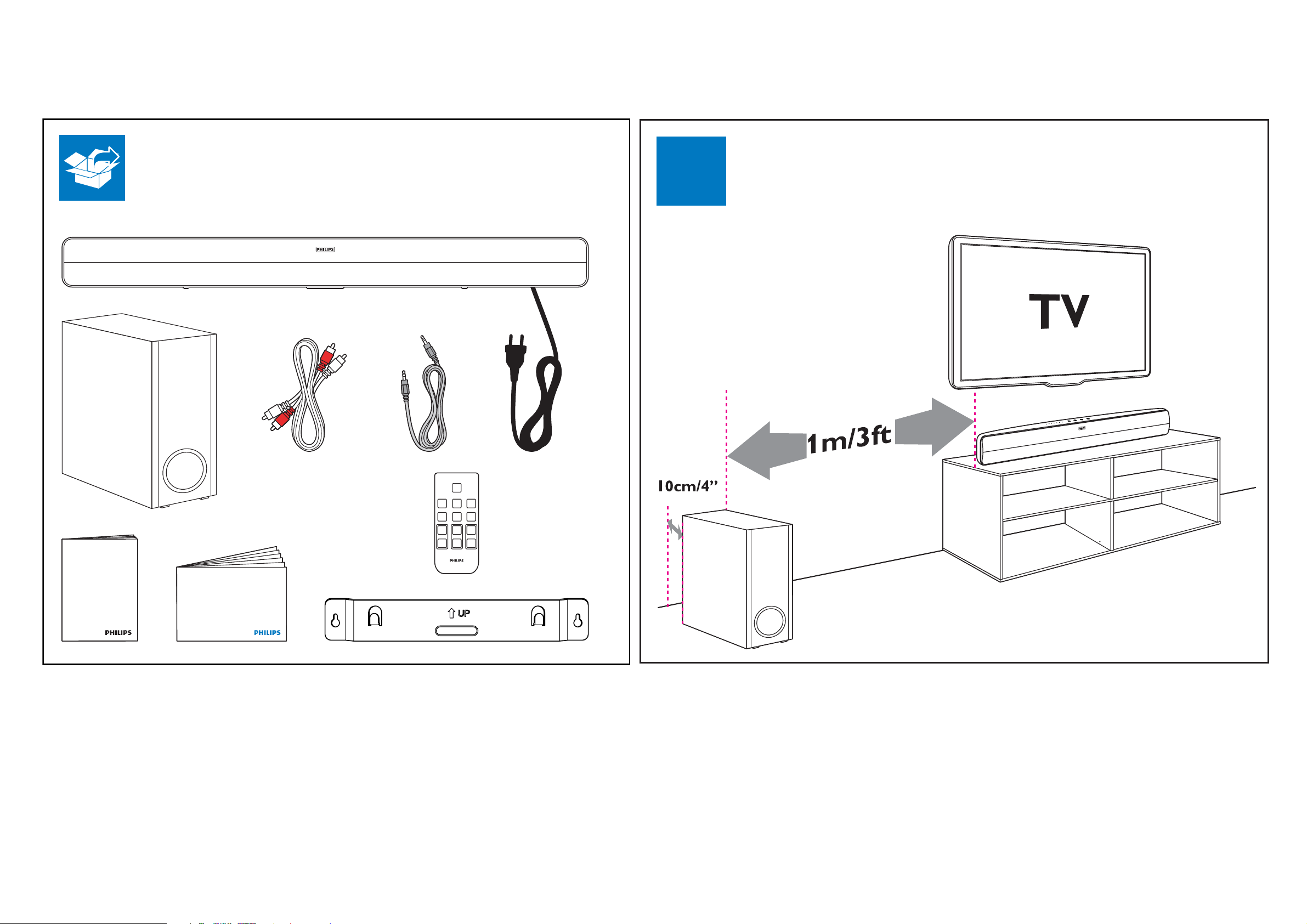
QUICK START GUIDE
The following excerpt of the QSG/DFU serves as an introduction to the set.
The complete Direction for Use can be download in the different languages from the internet site of Philips Consumer care Center: www.support.philips.com
1
EN What’s in the box
EN Speaker placement
User Manual
Quick start guide
Page 12

2
EN Connect
4 - 2 4 - 2
1 2
3
EN Manage cables
Page 13

4
EN Switch on
1
4 - 3 4 - 3
5
EN Select your audio source
AUX
2
OPTICAL
Page 14

4 - 4 4 - 4
COAXIAL
2x
EN Wall mount the soundbar
1
2x
2.5cm
MP3
LINK
~14cm/5.5”
Page 15

EN For more information about using this product,
visit www.philips.com/supplort
2 3
4 - 5 4 - 5
Non-contractual images. / Images non contractuelles. / Außervertragliche Bilder.
All registered and unregistered trademarks are proper ty of their respective owners.
Speci? cations are subject to change without notice
Trademarks are the proper ty of Koninklijke Philips Electronics N.V. or their respective owners
2011 © Koninklijke Philips Electronics N.V. All rights reserved
www.philips.com
sgtt_1036/12,05,55,78,98_v1
Evite o uso prolongado do aparelho com volume
superior a 85 decibéis, pois isto poderá
prejudicar a sua audição.
Potência total de saída de 800W RMS, 10% THD
Page 16

BLOCK DIAGRAM
5 - 1 5 - 1
MP 3-IN
AUX-IN
MP3- L
MP3- R
AUX1 - L
AUX1 - R
CD4052B
AUX
Switch
IC 4558
PCM1808PW
ADC
Audio L/ R
SC KI
switch control
MCU- Debug Port
Debug1
Debug2
GN D
+3.3V
UART Po rt
For SW -Upgrade
STBY /ON
MC U
ST M8S207R8
LQFP64 / 64K B
Hi Sp eed SPI
I2 C
Mu
Top Key B oard ( A/D Key )
Standby
te
Sour ceStandby Vol ume- Vol ume+
Volu me- Volu me+
Fr ont LED Boar d
IR
I2C
Mute
Top LED Board
AUX1 CoaxialOptica lMP3
PSU Board
power supply uni t
Power consumption<1.0W
Power Output: 30Wx2+40W
SPK (Ω)
SU B
3 Ω
4 Ω
R//R L//L R//RSU B
L//L
4 Ω 40 W 30 W
Dolb y DTS
STBY /ON
BK +3.3V
+12V
+5V
+29V
OUTPUT THD 30%
Tweet er
DVS
30 W
OPTICAL
COAXIAL
+5V
A-DO
A- BCK
A-L RCK
CS8422
SPDIF IN
AP1117E33
AP1117E18
XT I
I2C
+3.3 V
.8 V
+1
XT AL - OUT
(DAI 2 Port )
P- DOUT
P-L RCK
P-BCK
For DSP- Debug
DS P- Re st
SC P-MO SI
SC P-MI SO /S DA
SC P-CL K
DS P- BS Y
DS P- CS
DS P- IR Q
GN D
CS495313
Audio DSP
Dolby Digital
Dolby PL II
DV S
DTS Digital Surround
EQ/Auto Volume
DAO
DA1
MC LK
L RCK
BCK
CRYST AL
24.576MHz
Main Board
Volume
TAS5086
D-AMP PW M
SE
SE
PWR AMP
TAS5342L
SE
Tweeter
SU
R CH
L CH
B
Page 17

WIRING DIAGRAM
5 - 2 5 - 2
CN302
V2
V4
VWA010032-0001
VSW323462-030R
VFC100320-1200
VFC050320-1300
VFC060320-1700
V3
V1
VFC250320-0600
VWA010032-0001
Page 18

6 - 1 6 - 1
INTERNAL IC DIAGRAM - CS495313
MAIN+MP3+IR BOARD
TABLE OF CONTENTS
Internal IC Diagram ...........................................................................6-1
Circuit Diagram (Part one) ................................................................. 6-2
Circuit Diagram (Part two) ................................................................. 6-3
PCB Layout Top View .......................................................................6-4
PCB Layout Bottom View .................................................................. 6-5
Serial
Control 1
12Ch,Audio In/
6Ch,SACD In
Serial
Control 2
Paraliel
Control
D M A
32-bit
DSP A
S/PDIF
16Ch PCM
Audio Out
S/PDIF
PX Y
Ext. Mem ory Controller
INTERNAL IC DIAGRAM - TAS5342LADDV
U ART
P
G PIO
32-bit
DSP B
XY
D eoug
STC
TMR1
TMR2
PLL
Page 19

CIRCUIT DIAGRAM (part one)
6 - 2 6 - 2
C319 B1
C320 B1
C321 B1
C322 B1
C323 C1
C324 C1
C327 B1
C328 C1
C329 C1
C330 C1
C331 C1
C332 C1
C333 C1
C334 B4
C335 B4
C336 B4
C337 B4
C500 A4
C501 A4
C503 A4
C504 A4
C508 A2
C509 A3
C510 C3
C512 A2
C517 A1
C518 B3
C520 B3
C523 A1
C524 A4
C525 A4
C526 B2
C527 A2
C528 B3
C529 A3
C530 A3
C531 A3
C540 A2
C541 C2
C542 D2
C543 D2
C544 D2
C545 D2
C546 D3
A
C547 D3
C548 D3
C549 B3
C550 D3
C551 D4
C552 D4
C572 A2
C578 B1
C581 B1
C589 B1
C590 A1
C593 A2
C597 A1
C602 A1
C603 A1
C604 B1
C607 A1
C608 A3
C610 B2
C611 B2
C616 B3
C617 B3
1234
C618 D3
C619 D3
C620 D4
C621 D4
C633 A1
C634 A4
C635 A4
C636 A1
C638 A4
C639 B2
C640 A4
C641 B2
C642 C2
C643 C2
C644 C2
C645 B2
C646 B2
C649 B2
C650 B2
C651 B2
C654 B2
C655 B2
C656 A4
C657 A4
C658 A1
C659 C4
C660 C4
C661 A2
C662 A2
C666 A4
C667 A4
C691 D3
C692 D3
C693 C4
C694 D4
C695 A4
C696 C2
C698 A4
C701 A2
C702 A2
C708 A2
C709 A2
C710 A2
C711 A2
C712 A2
C713 A2
C715 A2
CN303 B1
CN501 A1
CN503 A2
CN504 C2
CN505 A1
CN506 C2
CN507 A2
CN508 A2
CN511 C2
FB301 B4
FB302 B4
FB501 A2
FB502 A2
FB503 A1
FB504 A1
FB505 A2
FB506 A2
FB508 A1
FB514 C4
FB515 C4
FB516 C4
IC504 A4
IC505 D3
IC506 B4
IC509 C4
IC510 A3
JK301 B4
JK303 B2
JK501 B2
L503 B3
L505 D2
L506 D3
L507 C4
L512 B2
LD309 C1
LD310 C1
Q309 C1
Q310 C1
Q504 D3
R309 C1
R310 C1
R319 C1
R320 C1
R329 C1
R330 C1
R336 C1
R337 C1
R338 B4
R339 B4
R512 B1
R513 B2
R514 B2
R518 A4
R519 A4
R520 A4
R521 A4
R522 C4
R523 C4
R524 B4
R525 B4
R527 C4
R528 C4
R529 C4
R530 C4
R538 B1
R539 A1
R541 D4
R542 D4
R543 D4
R545 A2
R546 A2
R547 A4
R548 D3
R549 D3
R550 D4
R551 D4
R552 A3
R558 B2
R564 A4
R566 A4
R567 C3
R580 A4
R581 A4
R582 A4
R583 A4
R584 B2
R588 D2
R590 A4
R592 A4
R593 B2
R595 C2
R596 C2
R597 C3
R598 C3
R599 C3
R600 D3
R608 B2
R610 B2
R611 B2
R614 C2
R615 D3
R617 C2
R618 C2
R620 C3
R628 D3
R629 D2
R630 D2
R631 D2
R632 D2
R633 D2
R634 D2
R635 D2
R636 D2
R637 D3
R638 D2
R639 D2
R640 D2
R641 C3
R642 C3
R643 C3
R644 D3
R645 D3
R646 D3
R647 D3
R648 D3
R657 D3
R658 A4
R659 B4
R674 D3
R675 D3
R676 C3
R677 C3
R678 D4
R679 D4
R680 D4
R681 C4
R688 A3
R694 C2
R695 C2
R696 C3
A
R697 C3
R705 A2
R706 A2
R707 A2
R708 A2
R709 A4
R710 A4
R711 C2
R712 C2
R713 C2
R714 C3
R715 C3
R716 C3
R717 D2
R718 D2
R719 C3
RB304 B4
SN301 B1
XL501 C2
B
C
D
B
C
D
1234
Page 20

CIRCUIT DIAGRAM (part two)
6 - 3 6 - 3
C339 A4
C502 D3
C505 C3
C511 A1
C513 A1
C514 A1
C515 A1
C516 A2
C519 C4
C521 B2
C522 A3
C532 B2
C533 C3
C534 B3
C535 C3
C536 C3
C537 B3
C538 B3
C539 C3
C553 D1
C554 D1
C555 D1
C556 D1
C557 D1
C558 D1
C559 D1
C560 D1
C561 D1
C562 D1
C563 D1
C564 D1
C565 D1
C566 D1
C567 D1
C568 D1
C569 C1
A
C570 D1
C571 D1
C573 D3
C574 C3
C575 D3
C576 A3
C577 A3
C579 A2
C580 A2
C582 A3
C583 A3
C584 A3
C585 A3
C586 A2
C587 A2
C588 A2
C591 B3
C592 A3
C594 A3
C595 A3
C596 A3
C598 A2
C599 A2
C600 A2
C601 A2
C605 C4
C606 D2
C609 C4
C614 C4
C615 B4
C622 A3
C623 A3
C624 A3
C625 A3
C626 B3
C627 B3
C628 B3
C629 B2
C630 A3
C631 A3
C632 A3
C663 A4
C664 A4
C665 C2
C668 C1
C675 D3
C676 D3
C677 D3
C678 D3
C679 C1
C680 C1
C682 C1
C687 D2
C688 C3
C689 C3
C697 C1
C716 A2
C717 A2
CN502 A1
CN509A A4
D501 B4
D502 B4
D503 B4
D504 A4
FB512 A3
FB517 C1
FB518 A3
IC501 C4
IC502 B4
IC503 A1
IC507 B3
IC508 C3
JK502 A2
L501 B4
L502 D2
L508 A3
L509 A3
L511 A2
L513 C1
Q501 A4
Q502 A4
R501 A1
R502 A3
R503 A3
R504 A3
R505 A3
R506 A3
R507 A3
R508 A2
R509 A2
R510 A3
R511 A2
R526 A1
R531 B1
R532 B1
R533 B1
R534 C2
R535 C2
R536 C2
R537 C2
R540 B3
R544 C2
R553 B1
R554 B1
R555 C1
R557 B2
R559 A1
R560 A1
R561 A1
R562 A1
R563 A1
R569 C2
R570 C2
R571 C2
R572 A1
R573 A1
R574 B1
R575 B1
R576 B2
R577 A3
R578 B2
R579 B3
R591 A4
R594 A4
R601 B2
R602 D3
R603 D3
R604 D3
R605 D3
R606 D4
R607 A4
R621 B2
R622 B2
R624 B3
R625 B3
R626 C3
R627 B3
R649 C3
R650 D3
R651 C3
R652 D3
R653 D3
R654 D3
R655 D3
R656 D3
R661 B1
R662 C1
R666 B2
R667 B2
R668 C3
R669 C3
R670 C3
R671 C3
1234
A
R672 B3
R684 A2
R689 D3
R691 C3
R698 A3
R701 C3
R704 C3
R726 B4
R727 B4
R728 B4
R729 B4
R730 B4
R731 B4
XL502 B1
B
C
B
C
D
D
1234
Page 21

PCB LAYOUT - TOP VIEW
6 - 4 6 - 4
C323 A2
C324 A1
C339 A1
C505 B4
C513 B4
C514 A4
C515 B4
C518 B2
C519 B4
C520 B2
C521 B4
C522 B4
A
C523 A4
C524 B2
C525 A3
C526 B3
C528 B2
C529 A2
C530 A2
C531 A2
C532 B4
C533 A3
C534 B4
C535 B4
C536 B4
C537 B4
C538 B4
C539 B4
C543 A1
C546 B2
C549 B2
C551 B2
C573 A3
C574 B3
C575 A3
C588 A4
C589 B3
C592 B1
C594 B4
C595 A4
C596 A4
C598 B4
C599 A3
C601 A4
C603 A4
C607 B3
C608 A2
C609 B2
C610 B1
C611 B1
C614 B2
C615 B3
C616 B2
C617 B2
C618 B3
C619 B3
C620 B2
C621 B2
C622 A4
C623 A4
C624 A4
C625 A4
C626 B4
C627 B4
C628 B4
C629 B4
C630 A4
C631 A4
C632 A4
C634 B2
C638 B2
C640 B2
C642 A2
C643 A2
C650 B2
C651 B3
C654 B1
C655 B1
C658 B2
C660 B3
C664 B3
C679 B3
C680 A3
C687 B3
C688 B4
C689 B4
C691 B2
C693 B2
C695 B2
C697 B3
C701 A2
C702 A2
C708 B1
C709 B1
C710 B1
C711 B1
C712 B1
C713 B1
C716 A3
C717 A4
CN303 A2
CN501 A4
CN502 A3
CN503 A3
CN504 A2
CN505 A3
CN506 A1
CN507 A3
CN508 B1
CN509A A1
CN511 A1
D501 B3
D502 B3
D503 B3
FB501 A2
FB502 A2
FB503 A3
FB504 B4
FB505 B1
FB506 B1
FB508 B2
FB512 A4
FB514 B3
FB515 B2
FB516 B2
FB517 A3
FB518 A4
IC501 B2
IC502 B3
IC503 A3
IC504 B2
IC505 A3
IC506 B2
IC507 B4
IC508 B3
IC509 B2
IC510 A2
JK301 A1
JK303 B2
JK501 B1
JK502 A2
L501 B2
L503 B2
L506 B3
L507 B3
L508 A4
L509 A4
L511 A4
L512 B2
LD309 A1
LD310 A1
Q309 A2
Q310 A2
Q504 B4
R309 A1
R310 A1
R319 A2
R320 A1
R329 A2
R330 A1
R501 B4
R503 A4
R510 A4
R511 A4
R512 B4
R513 B1
R514 B1
R522 B2
R523 B2
R524 B2
R525 B2
R526 A3
R527 B2
R528 B2
R529 B2
R530 B2
R531 B3
R532 B3
R533 B3
R534 B4
R535 B4
R536 B4
R537 B4
R540 A4
R541 B2
R542 B2
R543 B2
R544 B4
R545 B1
R546 B1
R552 A2
R553 B4
R554 B3
R557 B4
R566 B2
R567 A3
R569 B4
R570 B4
R571 B4
R574 B4
R575 B4
R576 B4
R577 B4
R578 B4
R579 B4
R580 B2
R581 B2
R582 B2
R583 B2
R584 B2
R592 B2
R593 B3
R595 A2
R598 A2
R599 A2
R600 B3
R601 B4
R602 A3
R603 A3
R604 A3
R605 A3
R606 B4
R608 B2
R610 B1
R611 B1
R614 A3
R615 B3
R617 A3
R618 A3
R620 A3
R621 B4
R622 B4
R624 B4
R625 B4
R626 A3
R627 B4
R628 B3
R629 B2
R630 B2
R631 B2
R632 B2
R633 B2
R634 B2
R635 B2
R636 B2
R637 B3
R638 B2
R639 B2
R640 B2
R641 A3
R642 A3
R643 A3
R644 A3
R645 A3
R646 A3
R648 B3
R649 A3
R650 B4
R651 B4
R652 B4
R653 B4
R654 A4
R655 A4
R656 A4
R657 B4
R659 B2
R661 B3
R666 B4
R667 B4
R668 B4
R669 A3
R672 B4
R674 A3
R675 B2
R678 B2
R679 B2
R680 B2
R681 B3
R684 A3
R688 A2
R689 A3
R691 B4
R694 A3
R695 A3
R696 A1
R697 A1
R698 A3
R701 B4
R704 B4
R705 B1
R706 B1
R707 B1
R708 B1
R711 A3
R712 A3
R713 A3
R714 A3
R715 A3
R716 A3
R719 A3
RB304 A1
SN301 A2
XL501 A2
XL502 B3
1234
A
B
B
1234
Page 22

PCB LAYOUT - BOTTOM VIEW
6 - 5 6 - 5
C319 A2
C320 A2
C321 A2
C322 A2
C327 A2
C328 A2
C329 A2
A
C330 A2
C331 A2
C332 A2
C333 A2
C334 A1
C335 A1
C336 A1
C337 A1
C500 B2
C501 B2
C502 B3
C503 B2
C504 B2
C508 A3
C509 A3
C510 B3
C511 A3
C512 A3
C516 B4
C517 B4
C527 A3
C540 A3
C541 A2
C542 A2
C544 A3
C545 A2
C547 B2
C548 B2
C550 B2
C552 B2
C553 B3
C554 B3
C555 B3
C556 B3
C557 A3
C558 A3
C559 A3
C560 A3
C561 A3
C562 B3
C563 B3
C564 B3
C565 B3
C566 A3
C567 B2
C568 A3
C569 B3
C570 B3
C571 B3
C572 A3
C576 A4
C577 A4
C578 B4
C579 A2
C580 A2
C581 B4
C582 A4
C583 A4
C584 A4
C585 A4
C586 A3
C587 A3
C590 A4
C591 A4
C593 A3
C597 A3
C600 A4
C602 A3
C604 B2
C605 B2
C606 A3
C633 A3
C635 B2
C636 A2
C639 B2
C641 B1
C644 A2
C645 B1
C646 B1
C649 B2
C656 A2
C657 A2
C659 B3
C661 A3
C662 A3
C663 A3
C665 B3
C666 B2
C667 B2
C668 A3
C675 A3
C676 A3
C677 A3
C678 A3
C682 B3
C692 B2
C694 B2
C696 A2
C698 B2
C715 A3
D504 A3
FB301 A1
FB302 A1
L502 B3
L505 A2
L513 B3
Q501 B3
Q502 B3
R336 A2
R337 A2
R338 A1
R339 A1
R502 A4
R504 A4
R505 A4
R506 A4
R507 A4
R508 A3
R509 A3
R518 B2
R519 B2
R520 B2
R521 B2
R538 A2
R539 B4
R547 B2
R548 B2
R549 B2
R550 B2
R551 B2
R555 B3
R558 B2
R559 A3
R560 A3
R561 A3
R562 A3
R563 A3
R564 B2
R572 A3
R573 A3
R588 A2
R590 B2
R591 B3
R594 A3
R596 A2
R597 A3
R607 B3
1234
R647 A3
R658 B2
R662 B3
R670 B4
R671 B3
R676 B3
R677 B3
R709 B2
R710 B2
R717 A2
R718 A2
R726 A4
R727 A4
R728 A4
R729 A4
R730 A4
R731 A3
A
B
B
1234
Page 23

7 - 1 7 - 1
KEY BOARD
TABLE OF CONTENTS
Circuit Diagram ................................................................................. 7-2
PCB Layout Top & Bottom View ........................................................ 7-3
Page 24

CIRCUIT DIAGRAM
7 - 2 7 - 2
C316 B1
C317 B1
A
B
C318 B3
C325 B1
1234
C326 B1
CN302 A1
LD308 A4
Q308 B4
Q311 A3
R308 A4
R318 A3
R328 B3
R331 A2
R332 A2
R333 A2
R334 A2
R335 A3
TA301 B2
TA302 B2
TA303 B2
TA304 B3
A
B
1234
Page 25

7 - 3 7 - 3
PCB LAYOUT - TOP VIEW
CN302 A1 LD308 A1 TA301 A1 TA302 A2 TA303 A2 TA304 A3
123
A
123
PCB LAYOUT - BOTTOM VIEW
C316 A1 C317 A1 C318 A1 C325 A1 C326 A1 Q308 A1 Q311 A2 R308 A1 R318 A1 R328 A1 R331 A1 R332 A1 R333 A2 R334 A2 R335 A2
123
A
A
A
123
Page 26

8 - 1 8 - 1
+
-
POWER BOARD
INTERNAL IC DIAGRAM - SSC620S
TABLE OF CONTENTS
Internal IC Diagram ...........................................................................8-1
Circuit Diagram .................................................................................. 8-2
PCB Layout Top View .......................................................................8-3
PCB Layout Bottom View .................................................................. 8-4
INTERNAL IC DIAGRAM - AZ431AZ
CATHODE
REF
V
REF
ANODE
Page 27

CIRCUIT DIAGRAM
8 - 2 8 - 2
BD901 A1
C901 C1
C902 B1
C903 B1
C904 B1
C905 B1
C906 A1
C907 B2
C908 C2
C910 A1
C911 A1
C912 A1
A
B
C
C913 A1
C914 B2
C915 B2
C916 B2
C917 B2
C918 A1
"
4
31:
D
61:D
"
"
54
51:S
21:S
21:D
21:SWU
2
C919 A2
C920 A2
C922 C2
C923 C2
C925 B3
C926 B2
C927 B2
C928 B3
C929 B3
C930 B2
C931 B2
C932 B2
C933 B3
C934 A2
C935 A3
C936 A2
C937 A3
C938 A2
123
42
:
51:Q
1:Q
2
52
"
21:M
61:S
31:S
"
21:OD
D
32:D
"
C
21:E
3
51:D
"
23
S
71:
41:S
"
O
2
1:G
3
W573.1:D
B
MO
"
D:22
D:21
5
T
S:1:
HU:12
"
"
21:DU
"
3
Wdd
qvusbu
G0T
8
C939 A2
C940 A2
C941 B3
C942 B2
C944 B2
C945 B3
71:Q
41:Q
71:D
9
Hoe
GC
OD
2
4
41:D
[
C946 C2
CN901 C1
CN902 C1
CN904 C2
D901 B2
D902 B1
HU:13
6
uvP
7
qdP
21:DJ
81:S
21:E
S
S
B
D:29
34:S
[
B
D903 A2
D904 A2
D905 A2
D906 A2
D907 B3
D908 B2
84:
74:S
64:
DDW
E
4
1:E
:S
92
34
35
36
31:OD
31:
44:S
,37W
32
33
D909 A2
D910 C3
D911 B3
D912 B3
D913 A2
F901 C1
Q
"
41:R
H
14:S
82:S
72:S
62:S
52:S
2:S
4
S
32:
W
DD
,23W
28
29
2:
31
GT901 B1
GT902 A1
IC901 B1
IC902 C2
IC903 C2
IC903 C2
91:Q
8
:
1
D:2:
ET
21:E
26
27
61:E
E:14
FD
234
,6W
23
24
25
IC904 B3
L901 B1
L901 B1
L902 B2
L903 A2
L904 B2
D
94:S
18:S
28:S
38:S
:S
3:S
4
53:S
63:S
3:S
7
83:S
93:S
72:D
24:S
S
S
S:22
S:21
C
21:R
41:OD
5
CL4W4
TBGFUZ
:
21
22
:
54
33:
3:S
2
13:S
:2:
52:D
9
2
3
DDW
C
D:59
PO0PGG
8
"
13:D
"
E
FD
31:R
234
D:5:
GS,
7
NTC901 C1
Q901 B2
Q902 B2
Q903 B1
Q905 A3
Q906 A3
2
4
6
51:
5
D:28
7
31:E[
:3:S
81:
D
5
4
31:D
J
51:OD
5
75:D
GS.
3
4
5
6
Q907 A3
R901 C1
R902 C1
R903 C1
R904 C1
R905 C1
2
1:U
"
62:D
"
2
8
93
:
12
2
3
22
2
3
R906 C1
R907 B1
R909 B1
R910 B2
R911 B2
R912 B1
67:S
:
7
5
S
24
74:D
54:D
E
71:
42:
E
26:S31
91:E
D:41
48:S
:D
55
65
:S
33:D
R913 B1
R914 B1
R915 B1
R916 B1
R917 B1
R918 B1
15:D
:1
E
:
27:S
17:S
37:S
47:S
D:38
34
D:49
:6:S
46:S
36:S
4:D
3
:M
D:42
95:S
91:D
41:DJ
2
R919 B2
R920 B2
R921 B2
R922 B2
R923 A2
R924 A2
D:4:
56:S
D:53
55:S
43:D
45:S
R925 B2
R926 B2
R927 B2
R928 B2
R929 B2
R930 B2
Q
61:
1
3
:Q
1:M
4
D:46
F
D
61:R
C
66:S
1:M
5
D:3:
81:E
D:39
D:37
R931 B2
R932 B1
R933 B1
R934 A2
R935 A1
R936 A1
D:48
W32,
D:56
S:85
16:S
S:86
96:
S
44:D
W6,
R937 A1
R938 A2
R942 B3
R943 C2
R944 C2
R945 C2
S:87
S:88
R:18
FD
R946 B3
R948 B2
R950 B3
R951 B2
R952 A2
R953 A2
C
76:S
R954 A2
R955 A3
R956 B3
R957 A3
R958 A3
R959 A2
86:S
R960 A2
R961 A2
R962 A2
R963 A2
R964 A2
R965 A2
97:S
R
71:
C
FD
77:S
R966 B3
R967 B3
R968 A3
R970 A2
R971 A2
R972 A2
87:S
W73,
GGP0OP
R973 B2
R974 A3
R975 A3
R976 A3
R977 A3
T901 A2
A
TVR901 C1
ZD902 B2
ZD903 B1
B
4O5
2
J
75:S
D:36
;opjuqjsdtfE
;fubE
psqqB
;sfw
6
P
D
H
3
51:DJ
98:S
25:D
doJ!*obxjbU)!tdjopsudfmF!idfutbF
rab dnuoS
0102-62-.l
irpA
niL.LC
;O0Q;po!mfepN
;opjtjwfS
0.1
oaR.semaJ
4W4LC
E
W73,
W32,
W6,
L
901PC
35:S
32:
22:E
12:E
ZUFGB
T
C
2!
!!!!;fhbQ
2!!!!!!gp
!!;sfohjtfE;sfldfiD
neWiuGouL
123
Page 28

PCB LAYOUT - TOP VIEW
8 - 3 8 - 3
BD901 B2
C901 A1
C902 B2
A
C903 A3
C904 B1
C905 B1
C911 A2
C914 A3
C915 B3
C916 B2
C918 B3
C919 A2
C920 A3
C922 A3
C923 A4
C925 A4
C926 A4
C927 A3
C934 B4
C935 B4
C938 B4
C941 A4
C942 B4
C945 B4
C946 A1
CN901 A1
CN902 A4
CN904 A1
D903 B2
D904 B3
D905 A3
D906 B4
D907 A4
D908 A4
D909 B4
D911 A4
D912 A4
D913 B4
F901 A1
GT901 B2
GT902 B3
IC903 A4
IC903 A4
J901 A2
J902 A3
J903 B3
J904 A4
J905 A4
J906 A4
J907 A4
L901 B1
L901 B1
L902 A4
L903 B4
L904 B4
NTC901 A2
Q901 B3
Q902 B3
Q903 B2
Q905 A4
R909 B2
R918 A2
R955 A4
R959 A4
R973 A3
T901 B3
TVR901 A2
1234
A
B
B
1234
Page 29

PCB LAYOUT - BOTTOM VIEW
8 - 4 8 - 4
C906 B3
C907 B3
C908 A3
C910 B2
A
C912 A3
C913 B2
C917 B3
C928 A4
C929 A4
C930 A3
C931 A4
C932 A4
C933 A4
C936 B4
C937 B4
C939 B4
C940 B4
C944 A3
D901 B3
D902 A3
D910 A4
IC901 A3
IC902 A3
IC904 A4
Q906 A4
Q907 A4
R901 B1
R902 B1
R903 B1
R904 B1
R905 B1
R906 B1
R907 A3
R910 B3
R911 B2
R912 B2
R913 A2
R914 B2
R915 B2
R916 B2
R917 A2
R919 B2
R920 B2
R921 B2
R922 B2
R923 B2
R924 B2
R925 B2
R926 B2
R927 B2
R928 B2
R929 B3
R930 A2
R931 B3
R932 A3
R933 A3
R934 B3
R935 A3
R936 A3
R937 A3
R938 A2
R942 A4
R943 A4
R944 A3
R945 A3
R946 A3
R948 A3
R950 A4
R951 A4
R952 B4
R953 B4
R954 A4
R956 A4
R957 A4
R958 A4
R960 B4
R961 B3
R962 B3
R963 B3
R964 B4
R965 B4
R966 A4
R967 A4
R968 A4
1234
R970 A2
R971 A2
R972 A2
R974 B4
R975 B4
R976 B4
R977 B4
ZD902 B3
ZD903 B3
A
B
B
1234
Page 30

9- 1 9 - 1
LED BOARD
TABLE OF CONTENTS
Circuit Diagram ................................................................................. 9-2
PCB Layout Top & Bottom View ........................................................ 9-3
Page 31

CIRCUIT DIAGRAM
C309 A1
C310 A2
C311 A2
C312 A2
C313 A3
C314 A3
C315 A3
C340 A1
C341 A1
9 - 2 9 - 2
CN301 A1
LD301 A1
LD302 A2
LD303 A2
LD304 A2
LD305 A3
LD306 A3
LD307 A3
Q301 A1
Q301 A1
Q302 A2
Q302 A2
Q303 A2
Q303 A2
Q304 A2
Q304 A2
Q305 A3
Q305 A3
Q306 A3
Q306 A3
Q307 A3
Q307 A3
R301 A1
R302 A2
R303 A2
R304 A2
R305 A3
R306 A3
R307 A3
R311 A1
R312 A1
R313 A2
R314 A2
R315 A3
R316 A3
R317 A3
R321 A1
R322 A1
R323 A2
R324 A2
R325 A3
R326 A3
R327 A3
123
AA
123
Page 32

PCB LAYOUT - TOP & BOT VIEW
9- 3 9 - 3
C309 A1
C310 A1
C311 A2
C312 A2
C313 A2
C314 A3
C315 A3
C340 A2
C341 A1
CN301 A3
LD301 A1
LD302 A1
LD303 A2
LD304 A2
LD305 A2
LD306 A3
LD307 A3
Q301 A1
Q301 A1
Q302 A1
Q302 A1
Q303 A1
Q303 A1
Q304 A2
Q304 A2
Q305 A2
Q305 A2
Q306 A3
Q306 A3
Q307 A3
Q307 A3
R301 A1
R302 A1
R303 A2
R304 A2
R305 A2
R306 A3
R307 A3
R311 A1
R312 A1
R313 A1
R314 A2
R315 A2
R316 A3
R317 A2
R321 A1
R322 A1
R323 A2
R324 A2
R325 A2
R326 A3
R327 A2
123
A A
123
Page 33

Mechanical Exploded View
10 - 1 10 - 1
Audio
Stero
Note:A1=1+2+3
B1=14+15
C1=16+17
D1=19+20+21
RC
Page 34

REVISION LIST
Version 1.0
*Initial release
Version 1.1
*HTS3111/05 combine with HTS3111/12
11 - 1
Page 35

/12 /05
01
5 996510040098 PVC SHEET L65XW441XT0.5MM $ BFP121186-0001
01
6 996510040067 POWER PCB ASSY 100W $ ABE109060-0002
01
7 996510040105 SPEAKER DRIVER 2.5" 30W FSB113025-0401
01
8 996510040091 TWEETER DRIVER 1'' 30W 4 FSB143010-0401
01
9 996510040072 AC CORD BRACKET BPL110039-0001
01
10 996510040076 REAR COVER ASB BPQ100008-0001
01
13 996510040101 KEY PCB ASSY ABE109260-0001
01
18 996510040059 LED PCB ASSY ABE109270-0001
01
22 996510040094 RUBBER FOOT L25XW15XT4MM BRF100098-0001
01
A1 996510040114 FRONT PANEL ASSY ABN100050-0003
01
B1 996510040079 SKD BUTTON+STANDBY LIGHT GUIDE ABN100099-0001
01 C1 996510040065 SKD LED LIGHT GUIDE+LIGHT GUIDE ABN100099-0002
01
D1 996510040066 MAIN+MP3+IR PCB ASSY ABE109250-0001
01
D1 996510045168 MAIN+MP3+IR PCB ASSY ABE109250-0005
01
V1 996510040082 FFC CABLE 25P 60MM VFC250320-0600
01
V2 996510040061 FFC CABLE 5P 130MM VFC050320-1300
01
V3 996510040057 FFC CABLE 6P 170MM VFC060320-1700
01 V4 996510040068 FFC CABLE 10P 120MM VFC100320-1200
01
V5 996510040069 C/W 4P WHT-BLK-RD-BLK VWA010032-0001
01
11 996510040086 WALL MOUNT SECC GSE100934-0001
01
12 996510040097 RUBBER PAD L49XW7XT3MM BRF100099-0001
01
23 996510040075
PWR CORD 2P 1450MM
$ VPE003292-0010
01
23 996510045165
PWR CORD 3P 1450MM
$ VPE00A273-0050
01
Audio 996500023267
RCA CABLE 1200MM BLK OD2.6X5.2
VRC202001-1040
01 RC 996510040085 REMOTE CONTROL WIR113001-9501
01
Stereo 996510001598
STEREO CABLE
VMC700004-0060
01 SPKSUB -- SPK SUBWOOFER ESW194001-1101
002 SUBSPK 996510040089 SUBWOOFER ANW503111-CK01
002 SRF 996510010854 RUBBER FOOT -SUBWOOFER DUF503010-0012
MAIN+MP3+IR PCB ASS'Y
002 CN509A 996500015861 CONNECTOR B4B-XH-A 4 PIN CCN250000-0104
002 D501 996510010358 DIODE 1N4007 RAD114007-1010
002 D502 996510040102 DIODE 1N5819 1A 40V RAD115819-0020
002 D503 996510010358 DIODE 1N4007 RAD114007-1010
002 D504 996510010354 DIODE 1N4148W 100V SOD-123 CJ RCD114148-0012
002 FB504
996500012470
BEAD FERITE 100 OHM/ AT 100MHZ SFB001001-0030
002 FB512 996500012470 BEAD FERITE 100 OHM/ AT 100MHZ SFB001001-0030
002 FB518 996500012470 BEAD FERITE 100 OHM/ AT 100MHZ SFB001001-0030
002 IC501 Yes 996510027042 IC 3P LD1117AL-33-AA3 3.3V RCI111733-0005
002 IC501 Yes 996510040099 GS IC 3P AZ1117H-3.3TRG1 RCI111733-0002
002 IC502 Yes 996510027889 IC 3P LD1117AL-18-AA3 RCI111718-0005
002 IC502 Yes 996510027974 IC 3P AZ1117H-1.8TRE RCI111718-0004
002 IC503 996510027406 IC 128P CS495313-CVZ RCI495313-0001
002 IC504 996510034346 IC 8P JRC4558 SOP ART RCI004558-0004
002 IC505 996510040096 IC 64P STM8S207R8T6 LQFP AIC820786-C403
002 IC505 996510045167 IC 64P STM8S207R8T6 LQFP ST AIC820786-C408
002 IC506 996510040109 IC 14P PCM1808PW TSSOP TI RCI001808-0001
002 IC507
996510025677
IC 44P TAS5342LADDV HTSSOP RCI005342-0003
002 IC508 996510040104 IC 38P TAS5086 TSSOP TI RCI005086-0001
002 IC509 996510027429 IC 32P CS8422-CNZR RCI008422-0001
002 IC510 Yes 994000000841 IC 16PIN TC4052BFN RCI004052-1001
002 IC510 Yes 996510009894 IC 16P CD4052BM SOIC TI 4-CH RCI004052-1002
002 JK301 996510036924 PHONE JACK D3.6 3P L14XW6XH5 CJM036014-5020
002 JK303 996510015645 TOSL JK PLR131/T2 RECEIVER CJT200001-0009
002 JK501 996510000594 RCA JACK 3P WT/RD CJR003303-0010
002 L508 996510025463 INDUCTOR 22UH SIN003704-2200
002 L509
996510025463
INDUCTOR 22UH SIN003704-2200
002 L511 996510025463 INDUCTOR 22UH SIN003704-2200
002 LD309 996510025456 LED 3D 2P KED900003-0020
002 LD310 996510025456 LED 3D 2P KED900003-0020
002 Q309 Yes 994000000915 XISTR NPN 2SC1623 RCN201623-1001
002 Q309 Yes 996510027037 XISTR NPN 2SC5343SG RCN205343-0001
002 Q310 Yes 994000000915 XISTR NPN 2SC1623 RCN201623-1001
002 Q310 Yes 996510027037 XISTR NPN 2SC5343SG RCN205343-0001
002 Q501 996510000625 XISTR PNP 8550SL hFE160-300 RCP008550-0001
002 Q502 996510000580 XISTR NPN MMS8050L RCN008050-1001
002 Q504 994000000921 XISTR PNP 2SA812 HFE:200-400 RCP200733-1001
002 SN301 996510032507 IRT RECEIVER IRM-3638TF4 RHO363804-2003
002 XL501 996510015058 CHIP CRYST 12MHZ 30PPM 20pF JCQ313000-1260
Alternative
HTS3111
12NC
Description
Safety
Accessories Parts
Speakers Assembly Parts
PCM Code
Main Unit Parts
Level
Item No.
Page 36

/12 /05
Alternative
HTS3111
12NC
Description
Safety
PCM Code
Level
Item No.
002 XL502 996510028537 CRYSTAL 24.576MHz JCQ011002-2462
KEY PCB ASSY
002 LD308 996510020167 LED 3 DIA ULTRA RED TINT CLEAR KED200003-0180
002 Q308 Yes 994000000915 XISTR NPN 2SC1623 RCN201623-1001
002 Q308 Yes 996510027037 XISTR NPN 2SC5343SG RCN205343-0001
002 Q311 994000000921 XISTR PNP 2SA812 HFE:200-400 RCP200733-1001
002 TA301 996510005619 AI TACT SW SKHVBE3520 ALPS MAW060001-0010
002 TA302 996510005619 AI TACT SW SKHVBE3520 ALPS MAW060001-0010
002 TA303 996510005619 AI TACT SW SKHVBE3520 ALPS MAW060001-0010
002 TA304 996510005619 AI TACT SW SKHVBE3520 ALPS MAW060001-0010
POWER PCB ASSY
002 BD901 996510040074 BRIDGE RECTIF.GBP206 2A 600V $ RHD202060-0050
002 C901 996510029694 COND SAFETY 0.22uF 275V $ PVX2024G0-2240
002 C902 996510008283 COND SAFTY 0.1uF 250V +/-10% $ PVX2024F0-1042
002 C903 996500008286 COND MYLAR 0.022UF 100V 5% PRM0373A0-2230
002 C904 996500027115 CAP.SAFTY Y1 102PF 250V 20% Y5 $ PVY1025F0-1023
002 C905 996500027115 CAP.SAFTY Y1 102PF 250V 20% Y5 $ PVY1025F0-1023
002 C910 996510032497 CAP 1000PF 1000V 10% PZL4564Q4-1030
002 C911 996510040077 COND ELECT 82UF 400V $ PVE0994K0-8200
002 C912 996510032497 CAP 1000PF 1000V 10% PZL4564Q4-1030
002 C913 996510032497 CAP 1000PF 1000V 10% PZL4564Q4-1030
002 C914 996500032755 COND MYLAR 0.01 UF 100V 5% PRM0373A0-1030
002 C915 996510040112 COND ELECT 2.2UF 160V PME0995C0-2290
002 C916 996510040112 COND ELECT 2.2UF 160V PME0995C0-2290
002 C917 996510028531 CHIP CAP 220pF 500V PZL4564M0-2210
002 C919 996510030865 COND METAL 0.0022UF 630V 10% PVN0994P0-2220
002 C920 996500027115 CAP.SAFTY Y1 102PF 250V 20% Y5 $ PVY1025F0-1023
002 C923 996500016360 COND MYLAR 0.22UF 100V 5% PRM0373A0-2240
002 C930 996510028531 CHIP CAP 220pF 500V PZL4564M0-2210
002 C932 996510028531 CHIP CAP 220pF 500V PZL4564M0-2210
002 C933 996510012861 CHIP CAP 0.1uF 100V 10% PZL4564A0-1040
002 C934 996510040058 COND ELECT 2.2UF 100V PME0995A0-2290
002 C936 996510028531 CHIP CAP 220pF 500V PZL4564M0-2210
002 C940 996510028531 CHIP CAP 220pF 500V PZL4564M0-2210
002 C943 996510008284 CHIP CAP 1000pF 1000V 10% PZL4564Q0-1020
002 CN901 996500017458 CONNECTOR 3P P=3.96MM $ CCN396021-0103
002 CN904 996500015861 CONNECTOR B4B-XH-A 4 PIN CCN250000-0104
002 D901 996510010354 DIODE 1N4148W 100V SOD-123 CJ RCD114148-0012
002 D902 996510010354 DIODE 1N4148W 100V SOD-123 CJ RCD114148-0012
002 D903 994000000938 DIODE PR1507 1.5A 1000V RAD101507-1010
002 D904 996510012516 DIODEHER105 DO-411A400V50nSFMS RAD100105-0010
002 D905 996510021223 DIODE PR2007 2A 1000V DO-15CTC RAD102007-0010
002 D906 994000000938 DIODE PR1507 1.5A 1000V RAD101507-1010
002 D907 996510040102 DIODE 1N5819 1A 40V RAD115819-0020
002 D908 996510040108 DIODE SB260 2A 60V DO-15 RAD100260-0010
002 D909 996510032852 GS(S) DIODE FMX-G22S TO-220F RHD100220-0010
002 D910 996510010354 DIODE 1N4148W 100V SOD-123 CJ RCD114148-0012
002 D911 996500026949 DIODE SW 1N4148 PB<1000PPM RAD114148-1010
002 D912 996500026949 DIODE SW 1N4148 PB<1000PPM RAD114148-1010
002 D913 996510012516 DIODEHER105 DO-411A400V50nSFMS RAD100105-0010
002 F901 996510040113 FUSE 2A 250V $ KSE020200-0030
002 GT901 996500029309 ABSORBER BL YP-501M 500V 500A L $ RAU000501-1001
002 GT902 996500029310 ABSORBER BL YP-141N 140V 500A L $ RAU000141-1001
002 IC901 996510032491 IC 8P SSC620S SOP TAPE REEL RCI006200-0004
002 IC902 996510031429 CHIP OPTICAL SENSOR4P SOP $ RCO000817-3001
002 IC903 Yes 994000000952 IC 3P TL431 RHI004310-1001
002 IC903 Yes 996500029312 IC 3 PIN TL431 TO-92 CHANG JIAN RHI004310-1101
002 IC904 996510032504 IC 5P AP2125K-33TRG1 3.3V RCI212533-0001
002 L901 Yes 996510040093 LINE FILTER ET24 29MH JFT001002-0010
002 L901 Yes 996510040107 LINE FILTER ET24 29MH JFT001002-0011
002 L902 996500016694 6UH 13.5TS 2UEW SIL106002-6090
002 L903 996510012550 CHOKECOILS 10UH 10% P=5 CUT4MM SIL006019-1000
002 L904 996500015871 INDUCTOR 10 UH 10% SAN001600-1000
002 NTC901 996510040087 NTC THERMISTOR 5 OHM 3A $ RNT003002-5090
002 Q901 996510004298 XISTR NPN 2N5551B TO-92 RAN205551-1002
002 Q902 996510004298 XISTR NPN 2N5551B TO-92 RAN205551-1002
002 Q903 996510021085 MOSFET STK1060F TO220F AUK600V $ RHM001060-1001
002 Q905 996510012475 XISTR PNP 2N5401B TO-92 J. RAP205401-1002
002 Q906 994000000915 XISTR NPN 2SC1623 RCN201623-1001
002 Q907 994000000915 XISTR NPN 2SC1623 RCN201623-1001
002 T901 Yes 996510040081 SW TRANS EER28 6+6P 60W $ TSA000012-0104
002 T901 Yes 996510040111 SW TRANS ER28 6+6P 60W $ TSA000012-0108
002 TVR901 996510040095 VARISTOR 25A 470V $ RPT025001-0010
002 ZD902 996510020001 ZENER 24V 5% 0.5W RCZ005024-0010
Page 37

/12 /05
Alternative
HTS3111
12NC
Description
Safety
PCM Code
Level
Item No.
002 ZD903 996510031433 CHIP ZENER 18V 5% 0.5W (J3) RCZ005018-0010
LED PCB ASSY
002 Q301 Yes 994000000915 XISTR NPN 2SC1623 RCN201623-1001
002 Q301 Yes 996510027037 XISTR NPN 2SC5343SG RCN205343-0001
002 Q302 Yes 996510027037 XISTR NPN 2SC5343SG RCN205343-0001
002 Q302 Yes 994000000915 XISTR NPN 2SC1623 RCN201623-1001
002 Q303 Yes 994000000915 XISTR NPN 2SC1623 RCN201623-1001
002 Q303 Yes 996510027037 XISTR NPN 2SC5343SG RCN205343-0001
002 Q304 Yes 994000000915 XISTR NPN 2SC1623 RCN201623-1001
002 Q304 Yes 996510027037 XISTR NPN 2SC5343SG RCN205343-0001
002 Q305 Yes 994000000915 XISTR NPN 2SC1623 RCN201623-1001
002 Q305 Yes 996510027037 XISTR NPN 2SC5343SG RCN205343-0001
002 Q306 Yes 996510027037 XISTR NPN 2SC5343SG RCN205343-0001
002 Q306 Yes 994000000915 XISTR NPN 2SC1623 RCN201623-1001
002 Q307 Yes 996510027037 XISTR NPN 2SC5343SG RCN205343-0001
002 Q307 Yes 994000000915 XISTR NPN 2SC1623 RCN201623-1001
'V' means existing spare parts; "--" means non existing spare parts.
Revsion List:
1.0 25-Oct-10 Initial Released HTS3111/12
1.1 2-Jun-11
Addition of HTS3111/05 versions
Note : Only the parts with Philips 12NCs are normal Service spare parts.
 Loading...