

Page 1

DVD Receiver
CLASS 1
LASER PRODUCT
HTS3100/05/12/51/75/93/98
1 Technical Specifications and Connection
Facilities 2
2 Measurements Setup, Service Aid &
Lead Free Requirements 4
3 Service Hints 8
4 Directions For Use 9
5 Dismantling Instructions & Service Positions 11
6 Service Test Program 14
7 Block Diagram and Wiring Diagram 17
Block Diagram 17
Wiring Diagram 18
8 Circuit Diagram and PWB Layout 19
Front: Display 19
Front: Display (Top view) 20
Front: Display (Bottom view) 21
Front: Standby 22
Front: Standby (Top View) 22
Front: Standby (Bottom View) 22
MKI
Mono Board: Circuit Diagram (Part 1) 23
MKI
Mono Board: Circuit Diagram (Part 2) 24
This Service manual is for HTS3100/05/12/51/75/93/98 First and Second
Generation models.
For First Generation model (HTS3100/05/12/51/93/98), the serial number
begins with NW1A xxxx xxxx (PSCI) and VN1A xxxx xxxx (PACH).
For Second Generation model (HTS3100/05/12/51/75/93/98), the serial number
begins with NW2A xxxx xxxx (PSCI) and VN2A xxxx xxxx (PACH).
©
Copyright 2006 Philips Consumer Electronics B.V. Eindhoven, The Netherlands.
All rights reserved. No part of this publication may be reproduced, stored in
a retrieval system or transmitted, in any form or by any means, electronic,
mechanical, photocopying, or otherwise without the prior permission of Philips.
Contents PageContents Page
MKI
Mono Board: Circuit Diagram (Part 3) 25
MKI
Mono Board: Circuit Diagram (Part 4) 26
MKI
Mono Board: Circuit Diagram (Part 5) 27
MKI
Layout: Mono Board (Top View) 28
MKI
Layout: Mono Board (Bottom View) 29
MKII
Mono Board: Circuit Diagram (Part 1) 30
MKII
Mono Board: Circuit Diagram (Part 2) 31
MKII
Mono Board: Circuit Diagram (Part 3) 32
MKII
Mono Board: Circuit Diagram (Part 4) 33
MKII
Mono Board: Circuit Diagram (Part 5) 34
MKII
Layout: Mono Board (Top View) 35
MKII
Layout: Mono Board (Bottom View) 36
PSU Circuit Diagram 37
8 Overview - Modulator, Input/Output and
Headphone/Line Output Connectors 41
TAS5086-5142V6REF 41
Power Output Stage (SE) 42
Power Output Stage (BTL) 43
Power Supplies 44
Amp Board Layout : Topview 45
Amp Board Layout : Bottomview 46
9 Exploded View & Spare Parts List 47
Exploded View of the set 47
Spare Part List 48
10 Revision List 49
Published by KC-TE 0635 AV Systems Printed in the Netherlands Subject to modification EN 3139 785 31871
Version 1.1
Page 2
EN 2
3139 785 318711.
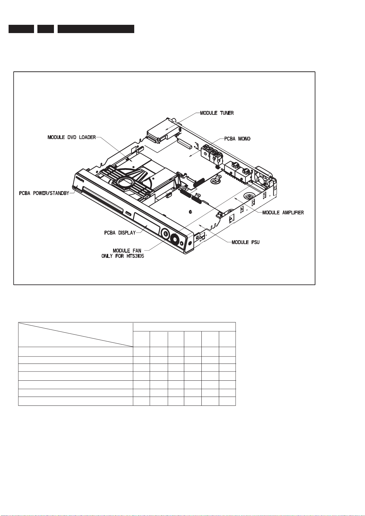
LOCATION OF PC BOARDS
Technical Specifi cations and Connection Facilities
VERSION VARIATIONS:
Type /Versions:
Features &
Progressive Scan
Line-Out
TV-In
Aux-In
Y/Pb/Pr (YUV) Component Video Output
CVBS
SCART
HTS3100
/05
/12
/51 /93 /98
/75
__
xx
__
xx
__
_
x
x
_
x
x
x
x
x
x
x
x
x
x
xxx
x
__
__
x
x
xx
xx
x
x
xx
HTS3100
Page 3

Technical Specifi cations and Connection Facilities
1. Specifi cations
3139 785 31871
1.
EN 3
1.1 General:
Mains voltage : 230V for /05, /12, /51
120V/230V for /55
/98
Mains frequency : 50/60Hz for /98, /55,
50Hz for /12, /05,
/51
Power consumption : 70W
< 1W Eco standby
power
< 70W at 1/8 P
(For main unit)
Dimension main unit : 360 x 54 x 324mm
rated
1.2 Tuner
FM
Tuning range : 87.5-108MHz
Grid : 50kHz for /12, /05, /51
100kHz for /98, /55
IF frequency : 10.7MHz ± 25kHz
Aerial input : 75Ω coaxial
Sensitivity at 26dB S/N : < 7μV
Selectivity at 600kHz bandwidth : > 25dB
IF rejection : > 60dB
Image rejection : > 25dB
Distortion at RF=1mV, dev. 75kHz : < 3%
-3dB Limiting point : 8μV
Crosstalk at RF=1mV, dev. 67.5kHz : > 28dB
Crosstalk at RF=1mV, dev. 40kHz : > 18dB
1.3 AMPLIFIER:
Output power
Front : 25W RMS / channel
Rear : 25W RMS / channel
Center : 50W RMS
Subwoofer : 50W RMS
Frequency response ±0.5dB : 20Hz-20kHz
Hum (Volume Minimum) : 200nW
Residual noise (Volume Minimum) : 40nW
Input sensitivity
Aux In : 1V ± 3dB at 22kΩ
Scart In : 0.5V ± 3dB at 22kΩ
Output sensitivity
Line Out (Left/Right) : 1V ± 2dB at 10kΩ
Scart Out (Left/Right) : 1V ± 2dB at 10kΩ
1.4 COMPACT DISC/VCD/DVD:
Video Decoding : MPEG-1/MPEG-2/
DivX 3/4/5/6 Vitra,
Video DAC : 12 Bits
Signal System : PAL / NTSC
Video Format : 4:3 / 16:9
CVBS Out
CVBS level : 1.0 ± 0.1V
Luminance S/N : >= 60dB
1)
p-p
MW
Tuning range : 531-1602kHz for /12,
/05, /51, /98, /93, /55
530-1700kHz for /98,
/55
Grid : 9kHz for /12, /05, /51,
/98, /55
10kHz for /98, /55
IF frequency : 450kHz ± 1kHz
Aerial input : Frame aerial
Sensitivity at 26dB S/N : < 4.0mV/M
Selectivity at 18kHz bandwidth : > 20dB
IF rejection : > 45dB
Image rejection : > 28dB
Distortion at RF=50mV, m=80% : < 5%
RGB/YUV Out
Amplitude : 1.0 ± 0.1V
S/N : >= 60dB
1)
Output terminals to be terminated with 75Ω
1)
p-p
Page 4
EN 4
3139 785 318712.
Measurements Setup, Service Aid & Lead Free Requirements
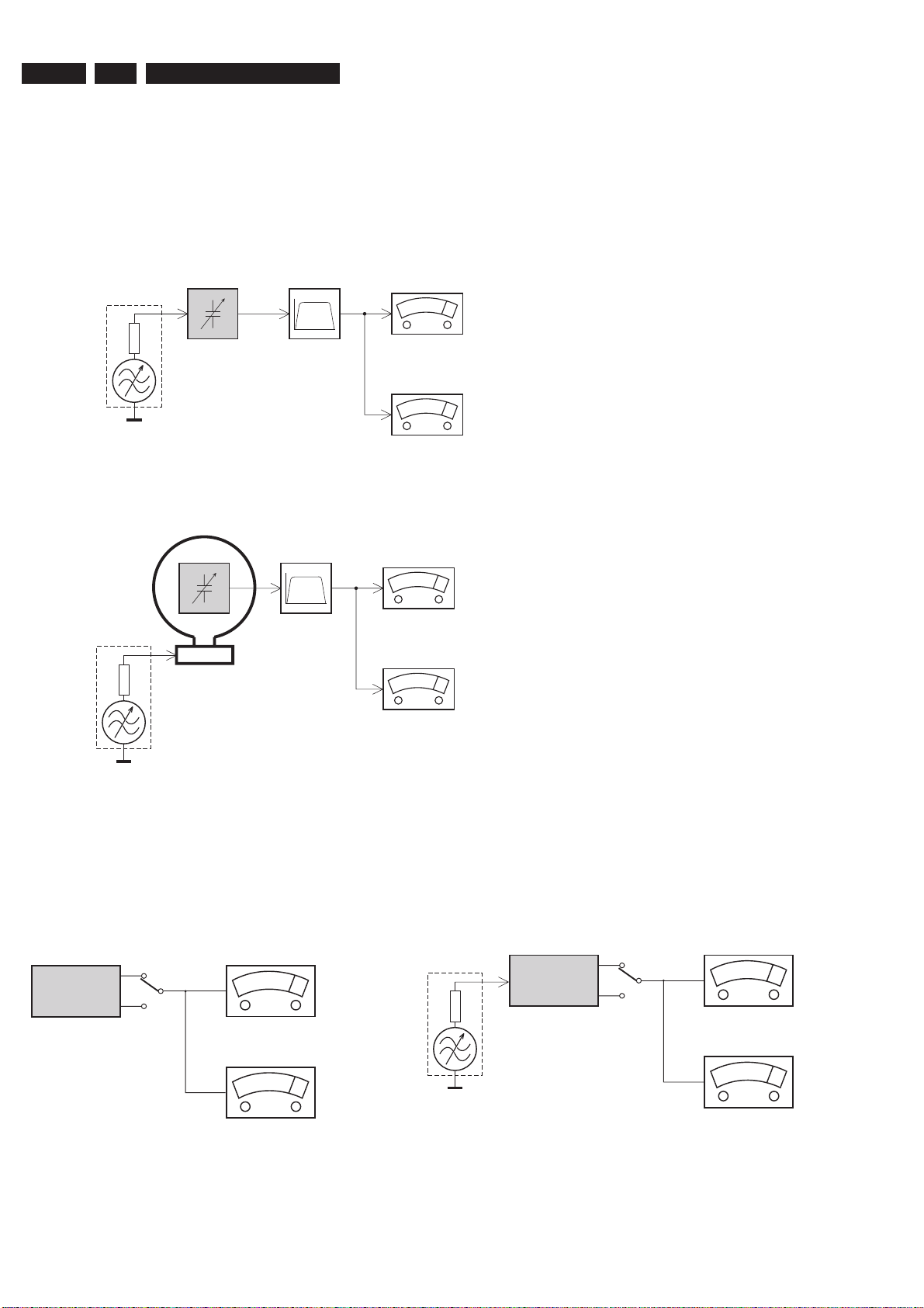
2. Measurements Setup, Service Aid & Lead Free Requirements
MEASUREMENT SETUP
Tuner FM
Bandpass
LF Voltmeter
e.g. PM2534
RF Generator
e.g. PM5326
DUT
250Hz-15kHz
e.g. 7122 707 48001
Ri=50Ω
S/N and distortion meter
e.g. Sound Technology ST1700B
Use a bandpass filter to eliminate hum (50Hz, 100Hz) and disturbance from the pilottone (19kHz, 38kHz).
Tuner AM (MW,LW)
RF Generator
e.g. PM5326
Ri=50Ω
DUT
Frame aerial
e.g. 7122 707 89001
Bandpass
250Hz-15kHz
e.g. 7122 707 48001
LF Voltmeter
e.g. PM2534
S/N and distortion meter
e.g. Sound Technology ST1700B
To avoid atmospheric interference all AM-measurements have to be carried out in a Faraday´s cage.
Use a bandpass filter (or at least a high pass filter with 250Hz) to eliminate hum (50Hz, 100Hz).
CD
Use Audio Signal Disc
(replaces test disc 3)
DUT
L
R
SBC429 4822 397 30184
S/N and distortion meter
e.g. Sound Technology ST1700B
LEVEL METER
e.g. Sennheiser UPM550
with FF-filter
Recorder
Use Universal Test Cassette CrO2 SBC419 4822 397 30069
or Universal Test Cassette
LF Generator
e.g. PM5110
Fe SBC420 4822 397 30071
DUT
L
R
S/N and distortion meter
e.g. Sound Technology ST1700B
LEVEL METER
e.g. Sennheiser UPM550
with FF-filter
Page 5
Measurements Setup, Service Aid & Lead Free Requirements
SERVICE AIDS
Service Tools:
Universal Torx driver holder .................................. 4822 395 91019
Torx bit T10 150mm ............................................. 4822 395 50456
Torx driver set T6 - T20 ......................................... 4822 395 50145
Torx driver T10 extended ...................................... 4822 395 50423
Compact Disc:
SBC426/426A Test disc 5 + 5A ............................ 4822 397 30096
SBC442 Audio Burn-in Test disc 1kHz ................. 4822 397 30155
SBC429 Audio Signals disc .................................. 4822 397 30184
Dolby Pro-logic Test Disc ...................................... 4822 395 10216
3139 785 31871
2.
EN 5
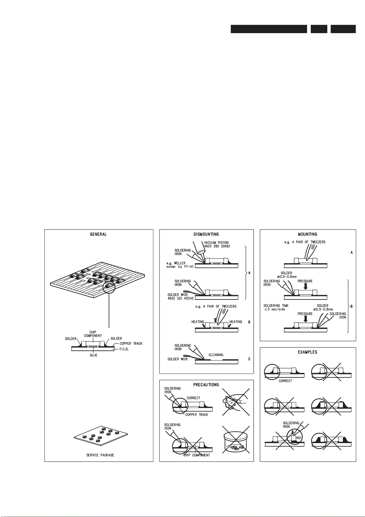
HANDLING CHIP COMPONENTS
Page 6
EN 6
3139 785 318712.
Measurements Setup, Service Aid & Lead Free Requirements
GB
All ICs and many other semi-conductors are
susceptible to electrostatic discharges (ESD).
Careless handling during repair can reduce life
drastically.
When repairing, make sure that you are
connected with the same potential as the mass
of the set via a wrist wrap with resistance.
Keep components and tools also at this
potential.
Tous les IC et beaucoup d’autres
semi-conducteurs sont sensibles aux
décharges statiques (ESD).
Leur longévité pourrait être considérablement
écourtée par le fait qu’aucune précaution n’est
prise à leur manipulation.
Lors de réparations, s’assurer de bien être relié
au même potentiel que la masse de l’appareil et
enfiler le bracelet serti d’une résistance de
sécurité.
Veiller à ce que les composants ainsi que les
outils que l’on utilise soient également à ce
potentiel.
F
WARNING
ATTENTION
GB
Complete Kit ESD3 (small tablemat, wristband,
connection box, extention cable and earth cable) ...........4822 310 10671
Wristband tester ....................................................................4822 344 13999
ESD
D
WARNUNG
Alle ICs und viele andere Halbleiter sind
empfindlich gegenüber elektrostatischen
Entladungen (ESD).
Unsorgfältige Behandlung im Reparaturfall kan
die Lebensdauer drastisch reduzieren.
Veranlassen Sie, dass Sie im Reparaturfall über
ein Pulsarmband mit Widerstand verbunden
sind mit dem gleichen Potential wie die Masse
des Gerätes.
Bauteile und Hilfsmittel auch auf dieses gleiche
Potential halten.
ESD PROTECTION EQUIPMENT:
NL
Alle IC’s en vele andere halfgeleiders zijn
gevoelig voor electrostatische ontladingen (ESD).
Onzorgvuldig behandelen tijdens reparatie kan
de levensduur drastisch doen verminderen.
Zorg ervoor dat u tijdens reparatie via een
polsband met weerstand verbonden bent met
hetzelfde potentiaal als de massa van het
apparaat.
Houd componenten en hulpmiddelen ook op
ditzelfde potentiaal.
Tutti IC e parecchi semi-conduttori sono
sensibili alle scariche statiche (ESD).
La loro longevità potrebbe essere fortemente
ridatta in caso di non osservazione della più
grande cauzione alla loro manipolazione.
Durante le riparazioni occorre quindi essere
collegato allo stesso potenziale che quello della
massa dell’apparecchio tramite un braccialetto
a resistenza.
Assicurarsi che i componenti e anche gli utensili
con quali si lavora siano anche a questo
potenziale.
WAARSCHUWING
I
AVVERTIMENTO
GB
Safety regulations require that the set be restored to its original
condition and that parts which are identical with those specified,
be used
Safety components are marked by the symbol
!
.
NL
Veiligheidsbepalingen vereisen, dat het apparaat bij reparatie in
zijn oorspronkelijke toestand wordt teruggebracht en dat onderdelen,
identiek aan de gespecificeerde, worden toegepast.
De Veiligheidsonderdelen zijn aangeduid met het symbool
!
F
Les normes de sécurité exigent que l’appareil soit remis à l’état
d’origine et que soient utiliséés les piéces de rechange identiques
à celles spécifiées.
Less composants de sécurité sont marqués
!
D
Bei jeder Reparatur sind die geltenden Sicherheitsvorschriften zu
beachten. Der Original zustand des Geräts darf nicht verändert werden;
für Reparaturen sind Original-Ersatzteile zu verwenden.
Sicherheitsbauteile sind durch das Symbol
!
markiert.
I
Le norme di sicurezza esigono che l’apparecchio venga rimesso
nelle condizioni originali e che siano utilizzati i pezzi di ricambio
identici a quelli specificati.
Componenty di sicurezza sono marcati con
!
CLASS 1
LASER PRODUCT
GB
Invisible laser radiation when open.
Avoid direct exposure to beam.
Osynlig laserstrålning när apparaten är öppnad och spärren
är urkopplad. Betrakta ej strålen.
SF
Avatussa laitteessa ja suojalukituksen ohitettaessa olet alttiina
näkymättömälle laserisäteilylle. Älä katso säteeseen!
DK
Usynlig laserstråling ved åbning når sikkerhedsafbrydere er
ude af funktion. Undgå udsaettelse for stråling.
S
Warning !
Varning !
Varoitus !
Advarse !
GB
After servicing and before returning set to customer perform a leakage
current measurement test from all exposed metal parts to earth ground to
assure no shock hazard exist. The leakage current must not exceed
0.5mA.
F
"Pour votre sécurité, ces documents doivent être utilisés par
des spécialistes agréés, seuls habilités à réparer votre
appareil en panne".
Page 7

Measurements Setup, Service Aid & Lead Free Requirements
2.1 Lead Free Requirements
3139 785 31871
2.
EN 7
Pb(Lead) Free Solder
When soldering , be sure to use the pb free solder.
INDENTIFICATION:
Regardless of special logo (not always indicated)
one must treat all sets from 1 Jan 2005 onwards, according next
rules:
Important note: In fact also products of year 2004 must be treated in
this way as long as you avoid mixing solder-alloys (leaded/ lead-free).
So best to always use SAC305 and the higher temperatures belong
to this.
Due to lead-free technology some rules have to be respected by the
workshop during a repair:
• Use only lead-free solder alloy Philips SAC305 with order
code 0622 149 00106. If lead-free solder-paste is required,
please contact the manufacturer of your solder-equipment.
In general use of solder-paste within workshops should be
avoided because paste is not easy to store and to handle.
• Use only adequate solder tools applicable for lead-free solder
alloy. The solder tool must be able
o To reach at least a solder-temperature of 400°C,
o To stabilize the adjusted temperature at the solder-tip
o To exchange solder-tips for different applications.
• Adjust your solder tool so that a temperature around 360°C
– 380°C is reached and stabilized at the solder joint. Heatingtime of the solder-joint should not exceed ~ 4 sec. Avoid
temperatures above 400°C otherwise wear-out of tips will rise
drastically and fl ux-fl uid will be destroyed. To avoid wear-out
of tips switch off un-used equipment, or reduce heat.
• Mix of lead-free solder alloy / parts with leaded solder alloy /
parts is possible but PHILIPS recommends strongly to avoid
mixed solder alloy types (leaded and lead-free).
If one cannot avoid or does not know whether product is leadfree, clean carefully the solder-joint from old solder alloy and
re-solder with new solder alloy (SAC305).
• Use only original spare-parts listed in the Service-Manuals.
Not listed standard-material (commodities) has to be
purchased at external companies.
• Special information for BGA-ICs:
- always use the 12nc-recognizable soldering temperature
profi le of the specifi c BGA (for de-soldering always use the
lead-free temperature profi le, in case of doubt)
- lead free BGA-ICs will be delivered in so-called ‘drypackaging’ (sealed pack including a silica gel pack) to protect
the IC against moisture. After opening, dependent of MSLlevel seen on indicator-label in the bag, the BGA-IC possibly
still has to be baked dry. (MSL=Moisture Sensitivity Level).
This will be communicated via AYS-website.
Do not re-use BGAs at all.
• For sets produced before 1.1.2005 (except products of 2004),
containing leaded solder-alloy and components, all needed
spare-parts will be available till the end of the service-period.
For repair of such sets nothing changes.
• On our website www.atyourservice.ce.Philips.com you fi nd
more information to:
BGA-de-/soldering (+ baking instructions)
Heating-profi les of BGAs and other ICs used in
Philips-sets
You will fi nd this and more technical information within the
“magazine”, chapter “workshop news”.
For additional questions please contact your local repair-helpdesk.
Page 8
EN 8
3139 785 318712.
Measurements Setup, Service Aid & Lead Free Requirements
2.2 Service Hints
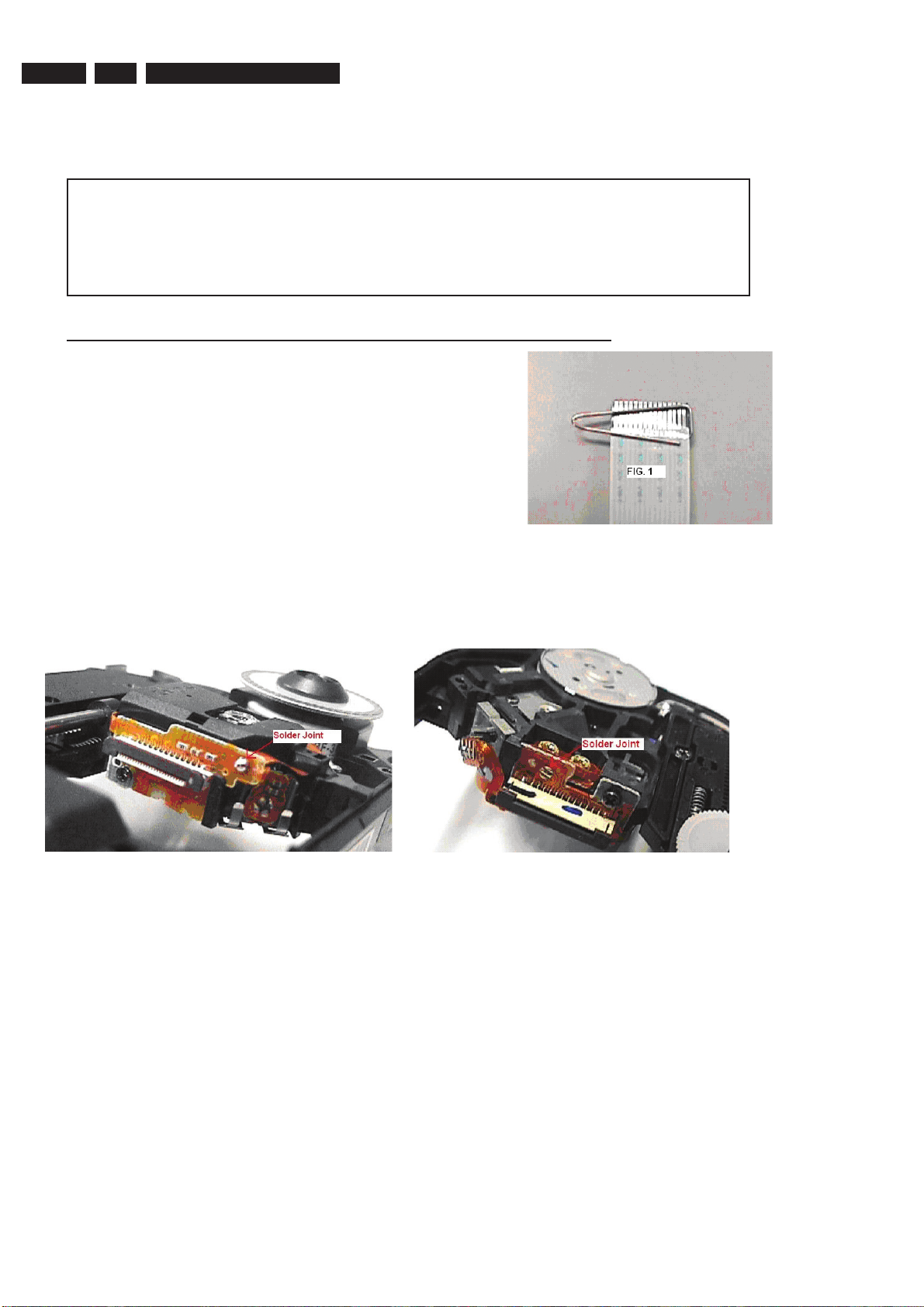
CAUTION
CHARGED CAPACITORS ON THE SERVO BOARD MAY DAMAGE THE DRIVE
ELECTRONICS WHEN CONNECTING A NEW DRIVE.THAT’S WHY, BESIDES THE SAFETY
MEASURES LIKE
• SWITCH OFF POWER SUPPLY
• ESD PROTECTION
ADDITIONAL ACTIONS MUST BE TAKEN BY THE REPAIR TECHNICIAN.
The following steps have to be done when replacing the defective loader :
1. Dismantling of the loader to access the ESD protection point if necessary.
2. Solder the ESD protection point*.
3. Disconnect fl exfoil cable from the defective loader.
4. Put a paper clip on the fl exfoil to short-circuit the contacts (fi g.1)
5. Replace the defective loader with a new loader.
6. Remove paperclip from the fl exfoil and connect it to the new loader.
7. Remove solder joint on the ESD protection point.
ATTENTION: The laser diode of this loader is protected against ESD by a solder joint which shortcircuits the laserdiode to ground.
Type 1 Type 2
(ESD protection point is accessible from top of loader) (ESD protection point is accessible from bottom of the loader)
*Only applicable for defective loader needed to be sent back to supplier for failure analysis and to support backcharging
evidence.
This is also applicable for all partnership workshops.
For proper functionality of the loader this solder joint must be remove after connection loader to the set.
Page 9
Directions for Use
AUDIO
OU
T
3139 785 31871
3.
EN 9
DVD HOME THEATRE SYSTEM HTS3100
Connect
1
Quick Start Guide
Enjoy
Set up
2
3
What’s in the box?
Scart cable
and 2 batteries
Remote Control
DVD system
User Manual
antenna
AM/MW loop
FM wire antenna
and subwoofer
1 centre, 2 front, 2 rear speakers
Set up
Finding the viewing channel
2
A
Connect the DVD system to TV
D
appears on the display panel.
A Press STANDBY ON on the DVD system.
B Press SOURCE on the DVD system until “DISC”
Television ( rear)
SCART IN
SCART IN
To off-air
antenna or
set-top box
button) until
°
screen
Select the display language on the
you see the blue DVD background.
Note To search for the correct viewing channel,
press the Channel Down button on the TV’s remote
select the correct viewing channel for the DVD
system.
C Turn on the TV. Use the TV’s remote control to
You should see the blue DVD background on the
A
DVD System (rear)
B
control repeatedly (or AV, SELECT,
TV.
B
Note It is important to connect the DVD system
directly to your TV. When watching the TV
programmes, you can press TV on the remote control
socket on this DVD system to the SCART IN socket
on your TV.
Use the supplied scart cable to connect the SCART
A
AC power outlet.
B Plug in the power cable from the DVD system to an
to get the sound output from the speakers system.
English
Dansk
Deutsch
Espanõl
Disc Lock
Display Dim
Program
OSD Language
Screen Saver
General Setup Page
The { General Setup Page } appears.
A Press SETUP.
Connect the audio from other
E
DivX(R) VOD Code
device to DVD system (optional)
Use the red and white audio cables (not supplied) to
connect the AUX IN (R/L) sockets on this DVD system
to the AUDIO output sockets on your Audio/Video
device (for example, DVD recorder, VCR).
Note The language set here is only for the menus
that are shown on the TV while operating this DVD
menu and press OK to confirm.
B Press to select { OSD Language } and press .
C Use keys to select a language option in the
AUDIO OUT
system, not for the DVD disc menu.
D Press SETUP to exit.
There are various setup options (Audio Setup, Video
Setup, Preference Setup) available on this DVD system.
b
DVD System (rear)
Refer to the user manual for more information.
Note Press AUX/DI on the remote control to get
the sound output from the speakers system.
Page 10
EN 10
AUDIO
OU
T
Set up
3139 785 318713.
Directions for Use
button) until
°
English
Dansk
Deutsch
Espanõl
Disc Lock
Display Dim
Program
OSD Language
Screen Saver
General Setup Page
DivX(R) VOD Code
2
Finding the viewing channel
A
appears on the display panel.
A Press STANDBY ON on the DVD system.
B Press SOURCE on the DVD system until “DISC”
select the correct viewing channel for the DVD
C Turn on the TV. Use the TV’s remote control to
A
Television ( rear)
SCART IN
SCART IN
Connect the DVD system to TV
D
To off-air
antenna or
set-top box
B
system.
You should see the blue DVD background on the
DVD System (rear)
control repeatedly (or AV, SELECT,
TV.
B
Note It is important to connect the DVD system
directly to your TV. When watching the TV
socket on this DVD system to the SCART IN socket
on your TV.
Use the supplied scart cable to connect the SCART
A
B Plug in the power cable from the DVD system to an
programmes, you can press TV on the remote control
AC power outlet.
The { General Setup Page } appears.
A Press SETUP.
to get the sound output from the speakers system.
screen
Select the display language on the
you see the blue DVD background.
Note To search for the correct viewing channel,
press the Channel Down button on the TV’s remote
Note The language set here is only for the menus
menu and press OK to confirm.
B Press to select { OSD Language } and press .
C Use keys to select a language option in the
D Press SETUP to exit.
AUDIO OUT
device to DVD system (optional)
Connect the audio from other
E
Use the red and white audio cables (not supplied) to
connect the AUX IN (R/L) sockets on this DVD system
to the AUDIO output sockets on your Audio/Video
device (for example, DVD recorder, VCR).
that are shown on the TV while operating this DVD
system, not for the DVD disc menu.
There are various setup options (Audio Setup, Video
Setup, Preference Setup) available on this DVD system.
Refer to the user manual for more information.
b
DVD System (rear)
Note Press AUX/DI on the remote control to get
the sound output from the speakers system.
2005 C Koninklijke Philips N.V.
All rights reserved.
12 NC 3139 245 22291
www.philips.com
Note This feature is only available for the rst time
setup. If you wish to reinstall all the radio stations, hold
PRESS PLAY”.
display panel.
Press TUNER.
Listen to radio
A
The display panel will show “AUTO INSTALL
All the available radio stations with strong reception
B Press PLAY until “START ...” appears on the
down the PROGRAM button on the remote control.
signal will be stored automatically.
preset radio station.
x until “FM/MW X DELETED” appears.
C Once complete, use . > keys to select a
D To delete a preset radio station, hold down STOP
channel.
DRAMA, ACTION or SCI-FI preset digital sound
effects.
Experience surround sound
A Press SURR to switch between stereo and multi-
B Press SOUND to select either CONCERT,
Enjoy
Note When you press PLAY button again, the
playback will resume from its last stopped point.
To start playback from the beginning, you have
to press STOP button two times to cancel the
to select an option in the menu and
3
Press OPEN CLOSE to open the disc tray.
Load a disc and close the disc tray.
Start disc playback
A
press PLAY to start playback.
B Playback will start automatically.
C If the disc menu appears, use keys
D Press STOP x to stop playback.
resume mode, then press PLAY button.
Troubleshooting
For more troubleshooting tips, see the user manual.
multi-channel surround output.
No picture.
• Press DISC button on the remote control.
• Check the connection to the TV and ensure the plugs are rmly in place.
No sound.
• Adjust the volume.
• Check the speaker connections and settings.
• Check the audio connections and press SOURCE button to select the correct input source.
• The centre and rear speakers operate only in multi-channel surround mode. Press SURR button to select
The DVD system does not work.
• Disconnect the power cord from the power outlet for a few minutes. Reconnect the power cord and try again.
Need help?
User Manual
See the user manual that cames with your Philips DVD System
Online
Go to www.philips.com/support
Page 11
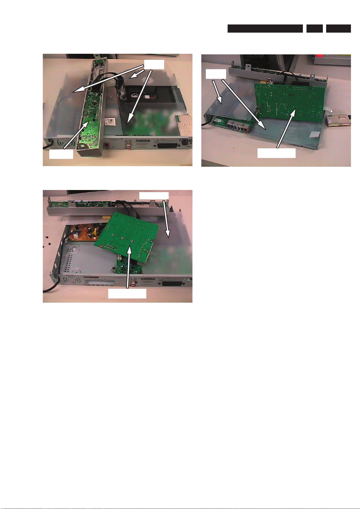
Dismantling Instructions & Service Positions
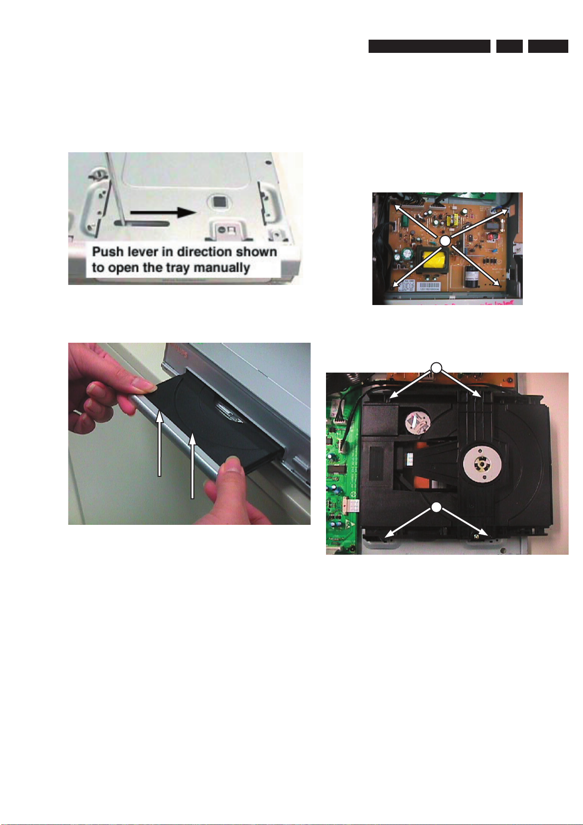
4. Dismantling Instructions
3139 785 31871
4.
EN 11
4.1 Dismantling of the DVD Loader Tray Cover
1) Insert a minus screwdriver and push the lever in the
direction as shown in Figure 4-1 to unlock the tray before
sliding it out.
Figure 4-1
2) Remove the Tray Cover as shown in Figure 4-2
4.2 Dismantling of the Front Board, PSU Module
& DVD Loader.
1) Release 4 snap hooks to remove the Front Board.
- 1 snap hook each on the left & right side
- 2 snap hooks on the bottom side
2) Loosen 4 screws A (See Figure 4-3) to remove the PSU
Module.
A
Figure 4 3
3) Loosen 4 screws B (See Figure 4-4) to remove the DVD
Loader.
B
Figure 4-2
B
Figure 4-4
Page 12
EN 12
3139 785 318714.
Dismantling Instructions & Service Positions
4.3 Dismantling of the Tuner Module & Mono
Board.
1) Loosen 1 screw C (See Figure 4-5) to remove the Tuner
Module.
Figure 4-5
2) Loosen 2 screws D and E (See Figure 4-6 & Figure 4-7)
to remove the Mono Board.
4.4 Dismantling of the Amp-module Board
1) Loosen 4 screws F and 2 screws G (See Figure 4-8 &
Figure 4-9) to remove Amp-Module Board.
C
G
Figure 4-8
H
D
Figure 4-6(AP) Figure 4-6(Europe)
F
Figure 4-7
E
H
Figure 4-9
Page 13
Dismantling Instructions & Service Positions
3.4 Service Positions
Insulation
Sheet
Insulation
Sheet
3139 785 31871
4.
EN 13
Front Board
Service Position - Front Board
Insulation Sheet
Amp Board
Service Position -Amp-Board
Mono Board
Service Position - Mono Board
Page 14
EN 14
A
A
3139 785 318715.
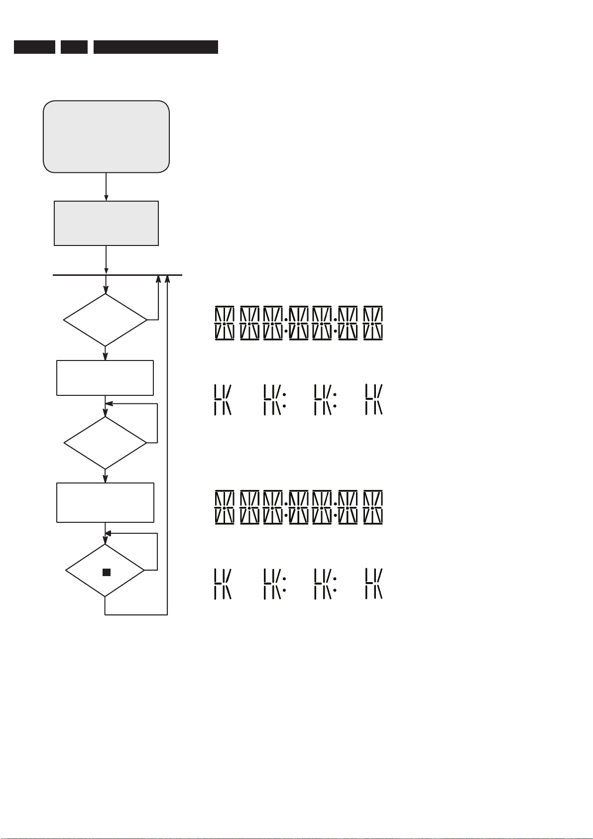
4. Service Test Program
Service Test Program
To start service test program
open the tray with remote control
or front panel key, while plugging
in the mains cord press 2, 5 8 on
remote control, the tray will close
by itself and the set will display
shown “S-Vxx-yy”
Display shows
“SERVICE”
followed by ROM version
“S-Vxx-yy”
Main Menu
Display Test
key
"DisplayTest"
triggered?
y
ctivate and display
"Pattern1"
n
S refers to Service Mode
V refers to Version
xx refers to Software version number of BEA
(counting up from 01 to 99)
yy refers to Software version number of Front uP
(counting up from 01 to 99)
4.1 Display Test
Purpose:
This test is used to check the driving circuits, the display and whether there are
any short-circuits, open-circuits or any other defects.
Player:
Following display patterns are used to test the display and its connections to μP.
Pattern 1:
- to check the open-circuits
Pattern 2: Alternate display control pins are on (Test Pattern: 0x55)
- to check the short-circuits on Data port
Default: All display control pins are ON
key
"DisplayTest"
triggered?
y
ctivate and display
"Pattern2"
key
" "
triggered?
y
n
Receiver: (HTS3100/3105):
Following display patterns are used to test the display and its connections to μP.
Pattern 1:
Default: All display control pins are ON
- to check the open-circuits
Pattern 2: Alternate display control pins are on (Test Pattern: 0x55)
n
- to check the short-circuits on Data port
Page 15

Service Test Program
3139 785 31871
5.
EN 15
4.1.1 Reprogramming of DVD version Matrix
After repair, the customer setting and region code may be lost.
Reprogramming will put the set back in the state in which it has left
the factory, ie. with the default setting and the allowed region code.
Model Region Region Code TV Type
HTS 3100/12 Europe 2 PAL
HTS 3100/51 Russia 5 PAL
HTS 3100/05 UK, Ireland 2 PAL
HTS 3100/75 Aust/NZ 4 PAL
HTS 3100/98 APAC 3 PAL
HTS 3100/93 China 6 PAL
To reprogram do as follows:
1) Power up the set and select DISC source.
2) Open tray by press “OPEN/CLOSE” button on the set or press
and hold “STOP” button on the RC.
3) Press the following buttons on the Remote Control:
<9> <9> <9> <9> <AUDIO> <0> ...........for HTS 3100/12
<9> <9> <9> <9> <AUDIO> <1> ...........for HTS 3100/51
<9> <9> <9> <9> <AUDIO> <2> ...........for HTS 3100/05
<9> <9> <9> <9> <AUDIO> <7> ...........for HTS 3100/75
<9> <9> <9> <9> <AUDIO> <4> ...........for HTS 3100/98
<9> <9> <9> <9> <AUDIO> <6> ...........for HTS 3100/93
4) The display shows ‘YYYY-ZZ’ and the tray will close.
YYYY = model number (eg. 8300, 8500, etc.)
ZZ = slash stroke version (eg. 01, 69, etc.)
4.1.2 Procedure for check Software version
1) Power up the set and select DISC source.
2) Open tray by press “OPEN/CLOSE” button on the set or press
and hold “STOP” button on the RC.
3) Press “DISPLAY” button on the Remote control.
4) The TV screen will shows:
PPPP-Vxx YYYYY-ZZ
SERVO: GGGGGGGG REG:DD
PPPP = HTS 3300MKII
xx = version number
YYYYY = model # - 3300D
ZZ = stroke version (12, 51, 05, 98, 55, 51K)
GGGGGGGG = version for servo code
4.1.3 Burning of fi rmware
1. Unzip the zip-archive attached with this service information.
2. Start the CD burning software and create a new CD Project
(Data disc) with the following settings:
a. File System: ISO9660
b. Format: MODE 2/XA
c. Recording format: Single Session (Track at once),
Finalized CD
3. Place the content of the zip-archive into the root directory of the
new CD project.
4. Burn the data onto a blank CDR or CDRW.
Note: ISO9660 is mandatory, UDF discs are not supported!
The fi nal CDROM must not contain any other data except
the fi le from the zip-archive.
4.1.4 Procedure to upgrade the fi rmware
1. Power up the set and open tray.
2. Insert the prepared Upgrade CDROM and close the tray.
3. The set will display:
LOAD -> MULTICH ->…………. ->UPG END.
The whole process takes less than 2 minutes.
Note: Do not press any button or interrupt the main supply upgrading
process,Otherwise the set may become defective.
4. When the upgrade is completed, the tray will close automatic.
5. The tray will close and the set will go to Standby mode
automatically when the upgrade process is completed.
4.1.5 Procedure to check the fi rmware version to confi rm
upgrading
1. Power up the set and open tray.
2. Press the <Menu Display> button on the Remote Control.
3. The fi rmware version will be displayed on the top left hand corner
of the OSD.
4.1.6 Trade Mode
Trade mode is a feature that will block all set keys when enabled. It is
for dealers to prevent customers fromremoving disc, changing source
etc using the set keys.Rotary and Remote Control (RC) keys are still
allowed inTrade mode.
To activate Trade Mode:
1) Power up the set and select DISC source.
2) Open tray by press “OPEN/CLOSE” button on the set
or press and hold “STOP” button on the RC.
3) Then press buttons <2> <5> <9> on the RC.
4) The display shows ‘TRA ON’ and the tray will close.
Trade Mode is now enabled.
To deactivate Trade Mode:
1) Power up the set and select DISC source.
2) Open tray by press and hold “STOP”button on the RC.
3) Then press buttons <2> <5> <9> on the RC.
4) The display shows ‘TRA OFF’ and the tray will close.
Trade Mode is now disabled.
4.1.7 Procedure to change Tuner Grid (/98, /55 only)
1 Press SOURCE to select “FM” or “MW”.
2 Press STANDBY ON to switch the
DVD system to standby mode.
3 Press STANDBY ON again to turn on
the DVD system and hold down S
button on the front panel.
➜ The display will show "GRID 9" or
"GRID 10".
Helpful Hint:
– GRID 9 and GRID 10 indicate that the
tuning grid is in step of 9 kHz and 10 kHz
respectively.
Note: Repeating the same action will toggle back to its previous
tuning grid setting.
Page 16

EN 16
Notes:
3139 785 318715.
Service Test Program
Page 17

EN 17
3139 785 31871
6
Block Diagram, Wiring Diagram
Block Diagram
MONO BD
3139-248-3380x (MKI)
3139-248-87651 (MKII)
200 W Power Amplifier
Front Board
HEF4052B
ERROR
PSU
CONTROL
HTS3100_block_duagram_MK2.pdf_2006_04_13
Page 18

EN 18
3139 785 31871
10
1
10
15169
1
Digital Datas (I2S & I2C &Control )
1
1
1
151 6
12
1
5
191415
2P-stand-by switch
AMPLIFIER BOARD
(3139 247 12701)
SP-
Sp+
LIMIT
GND
SL+
SL-
Port_S
TU_SCL
TU_SDA
TU_SD
TU_L
TU_Stereo
TU-R
NC/RDS
VCC
GND
+Vcc
+Vcc
+Vcc
GND_A
GND_A
GND_A
+12VL
+5VL
+5VL
GNDD
+5VL
+5VL
GNDD
+12VA
GNDA
-12VA
STBY
POW_DN
+12VL
GNDM
+5VL
+12VL
GND
+5V EV
-24V
LOAD-
LOAD+
TROUT
GND
TRIN
DVD LOADER
(3139 248 00181)
+5VL 1
+12VL
GND
+5V EV
-24V 5
FRONT BOARD(V63111)
9P EH TO FRONT
10P FFC TO TUNER
10 Port_S
I2S-CLK
I2S-DATA
TU_SD
TU_L
TU_Stereo
TU-R
NC/RDS
VCC
1 GND
1303
L-out
SCART
1501
1502YPb
PrCVBS
1302
AUX_IN
TV_IN
8001 313911103781(FFC FOIL 10P/120/10P AD FOLD)
MONO BOARD
(3139 248 3380x) (MKI)
(3139 248 87651) (MKII)
24P/220mm FFC
1 LOAD-
LOAD+
TROUT
GND
5 TRIN
5P/220mm PH
6P/180mm PH
1 SP-
Sp+
LIMIT
GND
SL-
6 SL+
4P PH BOARD-IN TO FRONT(MIC)
3139 248 87361 FR1 2-layer
3139 248 87371
5P EH TO Front
+12VA 1
MIC
GND
-12VA 4
1 +5VL
GND
+5VL
+5VL
GND-D
+12VA
GNDA
-12VA
STBY
POW_DN
+12VL
12 GND-M
12P EH TO PSU
Power Supply
(3139 247 12501
3139 247 12511)
1 GNDD
SCLK
GNDD
LRCLK
GNDD
MCLK
GNDD
SDIN1
GNDD
SDIN2
GNDD
SDIN3
GNDD
SDA
SCL
GNDD
/RESET
/SD
/TD
20 /PDN
20Pin FFC Cable
Video Circuit
MT1389
Analog SW
ADC
DAC
2422 542
00031/32
1300
1101 11 03 1102
1105
1301
1 +12AM
MIC
GND_A
4 -12AM
1400
1201
+5VL
+12VL
GND-A
GND-A
GND-A
+Vcc
+Vcc
+Vcc
FR C FL SR SL SW
1702
NC 9NCSTBYRCLR-CLK
GND
VSCK
VSDA
VSTB 1
1707
1 NC
NC
STBY
RC
LR-CLK
GND
VSCK
VSDA
9 VSTB
1703
1708
1 STBY
2 GND
STBY BD
(3139 243 3384X)
TUNER
TM10
1900
6.
Block Diagram, Wiring Diagram
Wiring Diagram
3100 block diagram_p.eps_022106
Page 19

EN 19
3139 785 31871
7
Front: Display
Circuit Diagram and PWB Layout
VEE
1
2
4
LED
SEG
SEG
1
VDD
DOUT
GRID
1
2
3
4
5
6
7
8
9
10
12
14
15
3
16
OSC
DIN
4
<1:6>
STB
KS
VSS
13
GRID <11:7>
2
3
4
6
5
3
2
1
11
CLK
KEY
3
2
1
4
SW
SEG
TO/FROM 1105 OF
D
E
F
G
H
I
1701 B9
1702 F2
1703 E2
1705 E5
1707 D2
1708 H2
-24V
+5V_Ever
# PROVISION
45678910111213
12
IR
I
A
B
C
10 11 12 13
A
B
C
D
E
F
G
H
123
1713 H9
1714 H8
1715 H9
1716 H8
2700 B3
2701 B4
2702 B5
2703 B5
2704 B5
2705 C4
2706 C6
2707 C6
3456789
2711 D10
2712 E9
2713 E9
2714 E9
2715 A12
2716 E3
2717 E3
2718 H3
2720 G3
2721 B9
2722 B10
2723 A11
MONOBOARD
1709 B2
1710 H8
1711 H7
1712 H8
2731 I8
2732 I9
2733 H3
2734 G11
3701 B3
3702 B3
3703 B5
3704 C5
3705 B6
3706 C6
3707 C7
3708 B7
VSTB
VOLA
2708 B6
2709 C7
3715 D10
3716 E7
3717 E8
3718 E8
3719 G12
3720 E10
3721 G4
3722 G12
3724 H3
3725 H4
3726 I4
3728 I7
STB_DET
2724 E11
2726 D11
2729 I7
2730 I8
3729 I7
3730 I8
3731 I9
3733 B10
3734 B10
3735 A11
3736 A11
3737 A12
3738 B12
3739 C7
3740 D4
3741 E6
3709 D5
3710 C9
3711 C12
3712 C9
3713 C12
3742 E6
3743 G12
4701 D6
4702 D6
4703 E5
4704 E5
5700 B4
6701 D10
6703 C5
6718 H10
6720 H10
7701 H2
VSDA
GND_MTK
VSCK
7702-1 B5
7702-2 B7
7703 C4
7704 G12
7705 A11
7706 B11
7707 B11
7708 E10
F701 E2
F702 E2
+5VL
VOLB
40kHZ
F703 E2
F704 E2
F705 E2
F706 F3
+5V_EV
F717 C12
F718 B2
F719 B2
F720 B3
F721 D2
F723 D2
F724 D2
F727 G3
F730 E11
F731 D11
F732 G3
F733 G3
F735 D2
GND
+12VL
GND_D
FROM 1500 OF MONOBOARD
FROM PSU
DISPLAY BOARD
F707 F3
F708 F3
F710 F3
F711 F3
F712 G3
F715 D10
F716 C9
3709
8K2
1K2
1714
3743
1715
SKQNAB SKQNAB
3K3
3718
3716
MGND
3K3
3K3
3717
9
1
2
3
4
143827
7
43
31
15
16
17
18
19
20
21
22
23
13
42
41
40
39
44
24
25
26
28
29
30
5
37
36
35
34
33
32
10
11
12
Φ
8
6
7708
PT6312BLQ
VFD
3725
2718
100n
10K
F723
F702
100n
2716
F704
F705
100p
2700
1K2
2K2
3702
3701
SKQNAB
1713
1
2
3
1708
WH03D-1
3731
F703
3728
4K7
150R
4K7
BC847B
3740
7703
47p
2704
MGND
68K
3703
F701
F719
10u2724
F711
F707
F730
F732
F735
F727
100n
220p
2731
2726
2717
100n
100R
3724
10p
2714
F721
F724
F720
F715
F718
1712
3730
4K7
SKQNABSKQNAB
1711 1716
SKQNAB
2
3
4
5
F706
1703
WH05D-1
1
F710
F716
6701
PDZ6.2-B
3737
10u
2721
4K7
2701
35V
100p
22u
5700
1u0
2706
BAS316
6720
3719
F717
470R
4704
4703
4K7
3729
470n
2703
BAS316
6703
3704
1K0
2K2
3734
4701
MGND
4702
4
5
OUT
1
VS
3
7701
TSOP4836ZC1
GND
2
1K0
3726
33n
1
B
3
C
245
2723
1705
EVEMC
A
220p
2729
2702
MGND
470n
10p
2713
10p
2712
5
66
77
88
99
NULL
1702
11
22
33
44
5
F733
F708
BAS316
6718
3713
33R
33R
37113710
33R
3712
2K2
3733
33R
10K
3721
3722
4K7
3720
56K
F712
2720
220p
220p
2730
1
2
4
5
MGND
1709
MSJ-035-11C B AG SR
4K7
3742
3741
1710
4K7
WH04D-1
1
2
3
4
SKQNAB
1707
1u0
2707
2734
100p
7704
BC847B
100n
2711
4
7702-1
LM833D
3
2
1
8
3707
47p
2709
3708
12K
1u0
1K0
MGND
2705
MGNDMGND
MGND
MGND
7702-2
LM833D
5
6
7
84
35V
2722
10u
1K0
3739
MGND
MGND
F731
100p
2708
3706
3K9
3705
12
P9
16V10u
2733
P15
18
5P26P37P48P59P610
P7
P8
11
NC321NC4
NC5
22
4
P1
P1013P1114P1215P1316P14
17
246G23
7G
1
F1
F1A
2
32
F2
F2A
31
19
NC2
20
291G282G273G264G25
5G
DSP
HNV-07SS54T
1701
2715
22p
10K
3738
3736
330R
3735
330R
7706
BC857B
7707
BC847B
BC817-25
7705
10K
3715
2732
STB_DET
VOLB
+5VSTBY
P(2)
220p
P(1)
P(15)
P(6)
P(5)
P(4)
P(3)
P(2)
P(14)
P(13)
P(12)
P(11)
P(10)
P(9)
P(8)
P(7)
+5VL
STB_DET
LED
+5VSTBY
LED
VGL+1
40kHZ
-V_FIL
+5VL
-24V
VGL+1
VGL-1
-24V
+12VL
+5VSTBY
40kHZ
+5VSTBY
G(7)
G(6)
G(5)
G(4)
G(3)
G(2)
G(1)
P(6)
P(5)
P(4)
P(3)
P(2)
P(1)
+5VL
VOLA
VOLB
VOLA
+5VL
+5VL
MIC
MIC
-12VAM
MGND
+5VAM
-12VAM
+5VAM
-12VAM
+5VAM
-V_FIL
VGL-1
P(1)
P(7)
G(1)
G(2)
G(3)
G(4)
G(5)
G(6)
G(7)
P(15)
P(14)
P(13)
P(12)
P(11)
P(10)
P(9)
P(8)
+12VL
3139 243 33782_DisplayBd_sh130_sh1.pdf_2005_11_16
Page 20

EN 20
3139 785 31871
7.
Front: Display (topview)
Circuit Diagram and PWB Layout
DisplayBd_Topview_33782.pdf_022106
Page 21

EN 21
3139 785 31871
Front: Display (Bottom view)
7
Circuit Diagram and PWB Layout
DisplayBd_Bottomview_33782.pdf_022106
Page 22

EN 22
3139 785 31871
Front: Standby
StdbyBd_Topview_33842.pdf_022106
StdbyBd_Bottomview_33842.pdf_022106
Front: Standby (Top View) Front: Standby (Bottom View)
7.
Circuit Diagram and PWB Layout
A
1
2
3
B3B-EH-A
12
3801
1801
470R
SKQNAB
A
1802
F801
F802
F803
1801 A2
1802 A1
2801 A1
3801 A2
6801 B2
F801 A1
F802 A1
F803 A1
B
2801
220p
6801
LTL-816EELC
3139 243 33842_StdbyBd_sh130_sh1.pdf_2005_11_16
12
B
Page 23

EN 23
3139 785 31871
7.
Circuit Diagram and PWB Layout
Mono Board: Circuit Diagram MKI (Part 1)
COM
OUT
IN
VIN3
VIN4
VINLOp
VINLOn
PREGND
PWRVCC
PREVCC
PS
VBIAS
SB
VIN1
VIN2p
VIN2n
PWRGND
HS_GND
OUTLn
OUTLp
OUT4n
OUT4p
OUT3n
OUT3p
OUT2n
OUT2p
OUT1n
OUT1p
VO2
1101 D1
1102 G1
1103 H1
1105 I9
1108 I10
2100 A3
2101 A3
2102 A8
2103 A12
2104 A11
2105 A13
2106 A13
2107 A7
2108 A8
2109 A9
2111 A3
2112 A3
2117 A8
123 5678910111213
12345678910
11 12 13
2113 A1
2114 H7
2115 A4
2116 H7
E
F
G
H
I
A
B
C
D
E
F
G
H
I
4
2121 A8
2122 A10
2123 A10
2126 D13
2127 B7
2128 B7
2129 B8
2130 B8
2131 B8
2132 B9
2133 B9
2134 A12
2135 A12
2138 B1
2139 B2
2140 B2
2141 B3
A
B
C
D
2146 B3
2147 B4
2148 B4
2149 B5
2151 B5
2152 B5
2153 B6
2154 B6
2155 B6
2156 B6
2157 B6
2158 B9
2159 B7
2160 B7
2161 B7
2162 B8
2163 B8
2164 B8
2118 A8
2119 A5
2120 A6
2169 C4
2170 C4
2171 C4
2172 C4
2173 C4
2174 C4
2175 B10
2179 F4
2180 E2
2181 F2
2182 G2
2183 G2
2184 H1
2185 H2
2186 H2
2187 I8
2188 I9
2142 B3
2143 B3
2144 B3
2145 B3
2196 G5
2197 G6
2198 G5
2199 G2
2200 C12
2201 C6
2202 C6
2203 C12
2204 C6
2205 C6
2206 C6
2207 C6
2208 C2
2209 C2
NB
2210 D5
2211 D3
2165 H5
2166 H5
2167 C2
2168 C2
2216 H5
2217 E5
2218 I2
2219 I2
2220 E6
2221 E5
2223 F4
2241 I7
2242 I8
2243 I8
2245 I9
2246 I9
2249 I11
2250 I10
NB :
2251 I11
3101 A12
2190 I10
2191 I11
2194 F5
2195 G5
3106 A9
3107 B9
3108 A7
3109 A10
3110 D13
3111 A10
3112 D13
3113 A13
3115 A12
3116 B11
3117 B11
3118 B9
3119 B7
3120 B11
3121 C12
2212 E2
2213 E5
2214 E2
2215 E5
3126 D4
3128 D3
3129 D2
3131 D12
3132 E3
3133 E2
3134 E3
3135 E2
3136 E5
3137 E5
3140 F4
3141 G5
3142 G5
3143 G2
3144 G5
3145 G1
3102 A13
3103 A5
3104 A12
3105 A13
3150 H5
3151 H9
3152 H9
3153 H9
3154 H10
3155 H10
3156 H10
3157 H10
3158 H5
3159 H5
3160 H2
3161 I11
3162 I2
3164 I8
3121 = 1K8 for high Z mode
3165 I8
3122 B11
3123 B11
3124 D12
3125 D13
3172 I11
3173 D2
3174 D2
3175 A10
3176 A12
3177 A11
3178 A13
3180 D13
3181 I8
3182 I8
3183 I8
3184 I8
3186 B10
3187 B10
3188 B10
3189 B10
3146 G5
3147 H1
3148 G1
3149 G2
4106 D6
4108 F6
4109 H10
4110 I9
4111 I9
5101 A8
5104 A1
5105 A2
5106 A3
5107 A4
5108 A6
5113 B7
5114 B8
5115 B8
5116 B9
5117 A1
3168 I2
3169 I2
3170 I11
3171 I10
5123 D2
5124 D4
5125 D3
5126 D5
5127 B2
6100 I10
6105 A1
6106 A1
7102 A2
7104 D4
7105 D3
7106 E2
7107 E3
7108 E3
7109 E9
7110 F3
7112 I11
4102 C6
4103 C6
4104 C6
4105 C6
F156 D6
T101 D1
T102 D1
T103 D1
T104 D1
T105 D1
T106 D1
T107 D1
T109 D1
T110 D1
T111 E1
T112 E1
T113 E1
T114 E1
T115 E1
T116 E1
T117 E1
5118 A2
5119 A4
5120 A5
5122 C2
T122 E1
T123 E1
T124 F1
T125 G1
T126 G1
T127 G1
T128 G1
T129 G1
T130 G1
T131 H1
T132 H1
T133 H1
T134 H1
T135 I1
F125 E12
F126 E12
F141 C6
F155 D6
T137 E6
T138 B9
T148 I8
T149 I8
T150 I8
T151 I8
T152 I8
T153 B10
T154 B10
T155 I10
T156 I10
T157 I10
T158 I10
T160 G4
T161 G4
T162 G4
T163 G4
T164 G4
T165 G4
T166 H5
T167 H5
T168 B10
T169 B10
T171 A1
T172 A3
T118 E1
T119 E1
T120 E1
T121 E1
T173 A3
T174 A1
T175 A3
T176 A4
T177 A5
T179 B2
T181 B4
T182 B4
T183 B4
T184 D4
T185 D5
T189 A5
T190 A6
T191 I11
T192 D4
T193 D3
T194 I11
T195 I10
T196 I8
T197 I8
T136 E6
2132 10u
T122
600R
4110
5127
150R 3101
4R73177
2250
1u0
D
10V
6100
BAS316
3151
2191 1u0
100R
2190 1u0
2158
470n
D
2184
220p
2120
27p
T183T179
T118
D
220p
2181
4111
47p
3111
2103
150R
3154
T182
10R
10n2165
2133 100n
1K03186
3141 27K
T173
27p
2119
220p2186
T195
4K7
3161
100n 2146
T175
3106
680K
T138
2141100n
F155
T185
T181
T184
D
10K 3168
2220 100n
3174 100R
2223 100n
330R3112
150R
3105
4106
123
4
47p 2134
B4B-PH-K
1108
2199470p
T113
2107 22p
47u 2210
3152100R
1K03162
3182 100R
100R3183
T194
D
T129
T128
T127
3145 1R0
T168
T169
2185 220p
T177
2164 47n
F141
T105
10n
2180
D
T151
2140
100n
100n
2144
5117
10K 3149
600R
T148
210647p
7106
BSH103
2175 10n
100n2127
47n
T152
2163
680K3136
3148330K
3129 390R
5122
600R
T112
T190
2147100n
T149
2123
47p
100n 2139
2218
470p
211422u
3155
T106
10R
2138
100n
100K3133
T101
T103
T150
100n
2112
5101
600R
150R
3104
1
2
3
4
5
6
1102
B6B-PH-K
23456
7
8
9
B9B-EH-A
1105
1
2159
100n
2154
100n
100n2130
T153
10n2179
22R
3124
31641K2
T192
315633R
2145100n
470p 2219
2135
47p
B5B-PH-K
1103
1
2
3
4
5
D
47p
2105
T191
47u
5106
600R
2167
4104
600R
T158
5114
600R
5123
220u2208
5126 600R
4105
3135 10K
T104
2202
1u0
10K
22K
3140
150R
3150
3109
10K3134
100n 2174
10K 3169
T116
T123
150R
150R3122
3123
100n 2170
600R
5115
2172
100n
4109
T166
T130
150R
3113
100R3173
T162
2160 100n
T154
100n2195
15K
3142
7105
2SB1132
100n
2214
100n 2115
1K0 3157
F156
2188
100n
212247p
2126 10n
1u02201
T156
T126
T124
3
4
5
6
7
8
9
2526
15
16
17
18
19
2
20
21
22
23
24
SFV24R-1ST
1101
1
10
11
12
13
14
T160
T161
600R
5107
470R
3125
3128
4R7
2142100n
94
UWR#95URD#
96
97
DVDD18_298UP1_299UP1_3
D
87
AD688IOA21
89
MB
9
ALE90AD791A1792IOA093DVSS_3
MA
DVDD3_280AD081AD182AD283AD384DVSS_285AD486AD5
HIGHA373DVDD3_1
HIGHA274HIGHA1
75
76
IOA2077IOCS#78IOA1
IOOE#
79
8
APLLVDD366IOWR#
A1667HIGHA7
68
69
HIGHA6
7
DVDRFIN
70
HIGHA571HIGHA4
72
59
HIGHA0
6
DVDRFIP
60
IOA18
61
IOA19
62
DVSS_1
63
APLLCAP
APLLVSS
64
65
51
TDO
DVDD18_1
52
53
IOA2
54
IOA3
55
IOA4
56
IOA5
57
IOA6
58
IOA7
44
USBP
USBM
45
46
USB_VDD3
FG
47
TDI
48
TMS
49
5
DVDD
TCK
50
37
DMO
FMO
38
39
TROPENPWM
4
DVDC
PWMOUT1
40
TRO
41
FOO
42
USB_VSS
43
3
DVDB
VREFO
30
31
FEO
TEO
32
TEZISLV
33
OP_OUT
34
OP_INN
35
OP_INP
36
253
OSN
254
RFGC
IREF
255
256
AVDD3
RFLVL
26
SGND
27
V2REFO
28
V20
29
246
RFRPAC
247
HRFZC
248
CRTPLP
249
RFGND
CSO
25
CEQP
250
CEQN
251
OSP
252
ADCVDD3
SVDD3
24
S_VCM
240
241
ADCVSS
242
S_VREFP
243
S_VREFN
RFVDD3
244
RFRPDC
245
JITFN
232
PLLVSS
233
IDACEXLP
234
PLLVDD3
LPFON
235
LPFIP
236
LPFIN
237
238
LPFOP
239
MC_DATA
225
SPDIF
RFGND18
226
227
RFVDD18
XTALO
228
XTALI
229
LDO1
23
230
JITFO
231
ASDATA0
ASDATA1
218
219
ASDATA2
22
LDO2
ASDATA3
220
DVDD18_6
221
ASDATA4
222
223
DVSS_13
224
21
MDI2
SPLRCK
210
211
SPBCK
212
DVDD3_10
ALRCK
213
ABCK
214
215
ACLK
216
DVSS_12
217
202
YUV5
YUV6
203
204
DVDD3_9
205
VSYN
206
YUV7
207
HSYN
208
SPMCLK
209
SPDATA
YUV2
197
DACVSSB
YUV3
198
199
DACVDDA
2
DVDA
MDI1
20
YUV4
200
DACVSSA
201
TPI
19
190
VREF
FS
191
192
YUV0
DACVSSC
193
YUV1
194
195
DACVDDB
196
RD22
DVDD3_8
182
183
RD21
184
RD20
185
RD19
186
RD18
187
RD17
188
RD16
189
DACVDDC
174
DVSS_11
175
RD25
176
RD24
177
DQM3
178
DQM2
179
TNI
18
RD23
180
181
DVDD3_7
RD31
168
RD30
169
CDFOP
17
RD29
170
RD28
171
RD27
172
DVDD18_5
173
RD26
160
RA8
DVSS_9
161
RA7
162
DVSS_10
163
164
RA6
RA5
165
RA4
166
167
153
RVREF
RCLKB
154
155
DVDD3_6
156
RCLK
CKE
157
158
RA11
159
RA9
16
CDFON
BA1
RA10
146
RA0
147
148
DVSS_8
RA1
149
15
SD
150
RA2
151
RA3
152
DVDD18_4
RWE#
CAS#
139
SC
14
RAS#
140
DVDD3_5
141
RCS#
142
143
BA0
DVSS_7
144
145
131
RD11
132
RD10
133
RD9
134
DVSS_6
RD8
135
DQS1
136
DQM1
137
138
RD1
124
125
RD0
126
RD15
127
DVDD3_4
RD14
128
RD13
129
13
SB
RD12
130
RD6
118
RD5
119
DVSS_5
12
SA
120
RD4
121
RD3
DVDD18_3
122
123
RD2
MD
11
110
PRST#
111
IR
INT0#
112
DQM0
113
DQS0
114
RD7
115
116
DVSS_4
117
UP1_6
102
103
UP1_7
104
UP3_0
105
UP3_1
106
UP3_4
107
UP3_5
DVDD3_3
108
ICE
109
7109
MT1389
1
AGND
10
MC
100
UP1_4
UP1_5
101
470p2194
T167
100n
2203
T164
2166 10n
47u
2169
2187
220p
3187 47R
2104
3103
47p
100K
47u
2211
T165
2118
T163
T172
1n0
100K
T131
3171
2SB1132
7104
10u 5124
214810u
T110
3172
100K
600R
5118
2217 2n2
15K3119
5105
3175
60R
3181
4R7
2213100n
100R
100n2128
3146 8K2
3184 100R
T135
10p
100n2121
2243
2149100n
3160 1K0
T107
100n2209
3170
47K
150R 3102
T137
60R
5104
2241 10p
2206 1u0
3115
150R
2116
T134
100n
T133
2200
100n
T114
3178
4R7
T189
F126
T125
2204 1u0
T132
2102 100n
60R
5120
100p
T196
2246
T176
BC847B
7112
2198 100n
T193
T121
56K
220p 2183
3144
F125
5108
27M
T197
47K
3110
3107
4108
100R
2152100n
100n
100p2245
2215
T171
33n2161
100p
2249
2221 2n2
100n
2212
217347u
6105
SS14
6106
SS14
2100100n
4102
2131
T111
100n
2162 1u0
3118
22R
D
470p
2216
3108
100K
2117 1n0
600R
5116
1K0 3165
31764R7
T120
680K
T157
3137
1u0
600R
5113
2205
T155
2111
BSH103
7107
100R
220u
600R
3153
5119
2197
1n5
22R
3131
2182
220p
10u 2151
2157
1K03143
100n
120p2207
150n2196
T102
100n 2153
5
4
23
24
26
27
6
25
7
22
1
10
21
8
9
28
2
3
13
14
11
12
18
17
16
15
20
19
7110
Φ
MM1646XH
29
30
3158 10K
100n 2143
390p2109
32
LD1117DT33
7102
1
T119
T136
150R3117
3116
150R
100n2129
2171
10K
47u
3159
25V47u
2113
7108
BC817-25W
3132
100K
3126 4R7
3147330K
22K
3180
100n2108
T109
10p2242
T174
T115
100n 2101
4103
2156
22R
3120
100n
10u 5125
3121
560R
T117
2155100n
220p
2251
3189 47R
47R3188
100n 2168
+3V3_D
+3V3_D
RDS_CLK
RDS_DAT
+3V3_D
STBY
STBY_DET
+5VL
+5V_STBY
+5M
+5V_STBY
+5VL
+4.5V
XTALI
PCM_LRCK
PCM_SCLK
PCM_MCLK
XO
AV_MUTE
+3V3_D
TU_SD
VSTB
+5VL
PCM_MIC_IN
+5M
VO2
V1P4
ADIN
LIMIT
+3V3_D
PCM_MIC_IN
MUTE_TV_
AMP_RST
+3V3_D
+L_V33
V1P4
+5M
+3V3_D
+3V3_D
+3V3_D
+S_V33
+5VL
+5D
+S_V33
+DV33B
+3V3_D
+V_V33
+3V3_D
+DV33B
+S_V33 +S_V33
+V18
+3V3_D
+DV33A
+DV33A
+V18
+V18
+3V3_D
+S_V33
+5V_STBY
+3V3_D
+1V8
VSDA
VSCK
VSTB
Source_sel_A1
PCM_LRCK
VSDA
VSCK
STBY_DET
RC6
SCL_DAC
SDA_DAC
S0_L3_0
PCM_LTRT
Erro_Det
V1P4
FOO
TROUT
TRIN
OP+
OP-
V1P4
FMO
VO2
V1P4
TRCLOSE
V1P4
TRO
DMO
V1P4
TROPEN
A_
Mot_stb
+5M
IOA
V1P4
V20
+S_V33
V20
V2P8
V2P8
V20
E
F
B_
D_
C_
IOA
+L_V33
+L_V33
B_
C_
D_
A_
CVBS
G_Y
V1P4
TxD
R_Cr
B_Cb
DQ(0:15)
MA(0:11)
AD(0:7)
AD(5)
AD(6)
A(21)
AD(7)
A(17)
A(0)
+V18
A(0:21)
A(9)
A(20)
PCE
A(1)
PRD
AD(0)
AD(1)
AD(2)
AD(3)
AD(4)
PWR
A(16)
A(15)
A(14)
A(13)
A(12)
A(11)
+DV33A
A(10)
A(5)
A(6)
A(7)
A(8)
A(18)
A(19)
+3V3_D
TRO
FOO
TROUT
TRIN
Mot_stb
TRCLOSE
+V18
A(2)
A(3)
A(4)
OPOP+
DMO
FMO
TROPEN
V1P4
ADIN
XO
XTALI
+DV33B
PCM_LR
PCM_LsRs
PCM_CLfe
+DV33B
S1_L3_1
E
+V_V33
F
+V_V33
+V_V33
MA(7)
MA(6)
MA(5)
MA(4)
+DV33B
+V18
MA(2)
MA(3)
+V18
+DV33B
DCLK
DCKE
MA(11)
MA(9)
MA(8)
WE
CAS
RAS
+DV33B
CS
BA0
BA1
MA(10)
MA(0)
MA(1)
DQ(15)
+DV33B
DQ(14)
DQ(13)
DQ(12)
DQ(11)
DQ(10)
DQ(9)
DQ(8)
LIMIT
DQM1
DQM0
DQ(7)
DQ(6)
DQ(5)
DQ(4)
DQ(3)
+V18
DQ(2)
DQ(1)
DQ(0)
Source_sel_A0
RxD
+DV33A
RC6
3139 243 33803_sh130_sh1.pdf_2006_01_13
Page 24

EN 24
3139 785 31871
7
Circuit Diagram and PWB Layout
Mono Board: Circuit Diagram MKI (Part 2)
11
1
0
13
12
9
8
9
10
VSS
VDDQ
1M-1
DQM
VDD
VSSQ
0
A
BA
1
6
H
0
WE
L
NC
CAS
RAS
7
5
4
3
2
15
14
11
10
CS
CKE
CLK
D
0
1
2
3
4
5
6
7
8
EN EN
19
0
1
2
3
4
5
6
7
8
9
10
11
12
13
14
15
16
17
18
19
VSS
VDD
0
A
D
5
2
4
RB
OE
CE
7
6
WE
3
1
RP
0
BYTE
2M-1 / 1M-1
NC
A-1
8
9
10
11
12
13
14
15
OSCO
RDSCL
SCOUT
VREF
RDDA
QUAL
VDDD VDDA
MPX
CIN
MODE
SYNC
TCON
OSCI
VSSA
VSSD
SCL
ADR
0
1
2SDA
WC
3
(SHEET1)
B
C
456789101112
(SHEET1)
D
E
F
G
12
456789101112
A
2253 B3
2254 B3
2255 C3
2256 C3
2257 C3
2258 C3
2259 C7
2260 C8
2261 C7
2262 C8
(SHEET1)
H
A
B
C
D
E
F
G
H
1201 C10
123
2263 C8
2264 D6
2265 E7
2266 E6
2267 F3
2268 F3
2269 E7
2271 C7
*
1202 C10
2110 C8
2252 A3
2273 G7
2274 C9
2275 G11
2276 E7
2277 E8
2279 A8
2280 A7
3203 A3
3204 G10
3209 B3
3210-1 B1
3210-2 D1
3210-3 D1
3210-4 D1
3211-1 D1
3211-2 C1
3211-3 C1
3211-4 C1
3212-1 C1
(SHEET1)
2272 G6
3214-2 E1
3214-3 E1
3214-4 E1
3227 E5
3229 E5
3233 F3
3234 E8
3235 F7
3236 F5
3237 F6
# RDS
4204 B7
4205 C6
4206 C6
5200 B3
5201 D6
5203 G6
7200 A2
7201 D3
7202 E6
7203 F2
3212-2 C1
3212-3 C1
3212-4 C1
3213-1 D1
3213-2 D1
3213-3 D1
3213-4 E1
3214-1 E1
T213 B9
T214 B9
T215 B9
T216 B9
T217 B9
T218 B9
T219 B9
T220 B9
T221 C9
T222 C9
T236 A3
T237 B2
3241 H3
3244 A9
3245 A9
3246 A8
3247 A9
4201 G2
4202 A8
4203 A8
# Refer to Table
* OPTIONAL
7206 A8
7207 A7
T201 F6
T202 A3
T203 B3
T204 E5
T205 F5
T210 A9
T211 A9
T212 B9
T238 F3
T240 D6
3238 G6
3240 H2
47p
2276
2259
22pD22p
2261
100n
2252
18
27
3214-1
10R
10R
3214-2
10R
3212-3
36
3212-4
10R
45
T222
D
T221
3
1
5
4
DD
74LVC1G125GW
7206
22
3
1
5
4
2277
1n0
74LVC1G125GW
7207
D
546124652
16
18
11427394349
28
41
8
10
11
13
42
44
39
15
36
40
38
19
2
4
45
47
48
50
51
53
5
7
29
30
31
32
33
34
20
21
17
37
1M X 16 X 4
DRAM
F
IS42S16400A-7TLI
23
24
22
35
25
26
D
7201
8
2268 100n
3213-1
10R
1
2274
22p
2279
100n
2280
100n
T240
2260
22p
3211-4
45
4201
36
10R
27
10R
3211-3
8
10R
3211-2
3212-1
10R
1
T205
T204
D
2272 47p
3247
D
47R
47R3246
T215
T216
T214
T213
220K
T212
3235
2262
22p
10R
27
10R
36
3213-2
3213-3
D
10K3244
100n2256
D
2257 100n
T237
D
36
3214-3
10R
2258 47u
16V
T219
T211
T218
4K73209
32
13
14
10
28
15
12
37
27
46
11
41
43
45
33
35
38
40
42
44
30
19
18
8
7
47
26
29
31
34
36
39
2
1
48
17
16
9
23
22
21
20
2Mx8/1Mx16
7203
M29W160ET70
25
24
6
5
4
3
[FLASH]
47K3237
3241 33R
T203
T202
D
T210
3234
10K
82p2273
22p
2275
6
11
3238 2K2
14
1
2
16
810
15
5
12
3
Φ
SAA6581T
7202
7
9
4
13
10R
18
3227
3211-1
D
1K0
600R
T238
5200
27
3212-2
10R
45
10R
3214-4
10K
3240
T217
2269 560p
45
2u22266
10R
3213-4
T236
T220
20
3
4
5
6
7
8
9
D
12
13
14
15
16
17
18
19
2
1201
1
10
11
4204
20FE-BT-VK-N
2263
22p
4205
4206
3245 10K
2254 100n
D
2253D100n
47K3236
22p
2110
3229 1K0
1
2
3
6
5
84
7
(2Kx8)
F
EEPROM
7200
M24C16-RDW6
D
D
600R
5201
10R
18
3210-1
9
D
4K73203
18
19
2
20
3
4
5
6
7
8
1
10
11
12
13
14
15
16
17
20FMN-BTRK-A
1202
2265
560p
4202
4203
2264
10R3233
D
100n
3210-3
36
D
10R
45
10R
27
3210-4
10R
3210-2
22p
2271
10K3204
2267 47u
16V
4M332
5203
T201
100n
+3V3_D +3V3_D
2255
RDS_CLK
TU_RDS_IN
PCM_MCLK
PCM_SCLK
SCL_DAC
PW_DN_
MUTE
+3V3_D
TD
PCM_LRCK
PCM_LR
PCM_LsRs
+5D
+3V3_FL
+3V3_D
+3V3_D
+3V3_D
AMP_RST
Erro_Det
SCL_DAC
SDA_DAC
+3V3_D
+3V3_D
DCLK
BA1
BA0
WE
CAS
MA(0:11)
DQ(0:15)
MA(0)
MA(11)
MA(10)
MA(9)
MA(8)
MA(7)
MA(6)
RAS
CS
DCKE
MA(5)
MA(4)
MA(3)
MA(2)
MA(1)
DQ(2)
DQ(3)
DQ(4)
DQ(5)
DQ(6)
DQ(7)
DQ(8)
DQ(9)
DQM1
DQM0
DQ(0)
DQ(1)
DQ(10)
DQ(11)
DQ(12)
DQ(13)
DQ(14)
DQ(15)
A(20)
AD(0:7)
A(21)
+3V3_FL
PRD
+3V3_FL
+3V3_FL
PWR
A(0:21)
A(0)
AD(2)
AD(3)
AD(4)
AD(5)
AD(6)
AD(7)
A(5)
A(6)
A(7)
A(8)
A(9)
A(10)
PCE
AD(0)
AD(1)
A(12)
A(13)
A(14)
A(15)
A(16)
A(17)
A(18)
A(19)
A(3)
A(4)
RDS_DAT
A(1)
A(2)
A(11)
TU_SD
TU_SD
+5D
SPDIF_IN
SPDIF_IN
PCM_CLfe
SDA_DAC
PCM_MIC_IN
PCM_MIC_IN
3139 243 33803_sh130_sh2.pdf_2006_01_13
Page 25

EN 25
3139 785 31871
7.
Circuit Diagram and PWB Layout
Mono Board: Circuit Diagram MKI (Part 3)
G4
0
3
2
VDD
VEE VSS
1
0
3
2
1
4X
030
1
M
AINL
MCLK
RST
1
0
AINR
GND REF_GND
VQ
LRCK
SCLK
FILT+
SDOUT
VLVD
VA
SDIN
SCLK
GND
VQ
FILT+
AOUTL
AOUTR
DEM
LRCK
MCLK
VA
F317 G3
F318 H2
F320 D2
F321 E2
F322 H2
F323 H2
F324 G3
T300 B6
T301 D6
T302 D6
T303 E7
T304 E7
T305 E14
T314 I5
T315 H13
T316 I13
T317 H10
T318 I10
T319 E10
T320 E10
F304 A1
F305 A2
F306 A2
F307 A2
F308 A2
F309 B2
F310 B2
F311 C2
F312 D2
F313 D2
F314 D2
F316 F3
6302 D10
6303 A11
6304 A9
6306 B10
6307 I5
7301 B3
7302 C7
7303 F11
7304-1 H8
7304-2 I8
7305-1 H3
7305-2 I3
7306 H12
7307 I5
7308-1 A10
7308-2 A11
7310 B10
F301 A2
F302 A2
F303 A2
3357 I8
3358 I9
3359 I9
3360 I10
3361 I4
3362 I4
3363 A9
3364 I6
3365 A9
3366 A10
3368 B9
4300 C3
4301 D3
4302 D10
4303 E14
4304 H2
4305 H2
4306 H2
4307 I2
5302 I13
5303 D9
6300 C3
6301 C3
3353 H7
3354 I13
3355 I3
3356 I4
3336 F4
3337 F7
3338 F4
3339 F5
3340 F5
3341 G4
3342 G4
3343 G5
3344 G7
3345 G5
3346 H8
3347 H9
3348 H9
3349 H10
3350 H4
3351 H3
3352 H4
3317 D8
3318 D8
3320 D4
3321 D9
3322 D8
3323 D11
3324 D11
3325 D3
3326 D4
3327 E8
3329 E4
3330 E14
3331 E13
3332 E3
3333 E4
3334 E4
3335 E7
2357 A11
2359 I4
2360 A11
2361 A9
2362 D12
3300 A3
3301 A3
3304 A3
3305 A4
3307 B2
3308 B4
3310 B3
3311 B6
3313 C6
3314 C7
3315 C7
3316 C4
2341 H7
2342 H11
2343 H11
2344 I11
2345 I7
2346 I13
2347 I10
2348 I9
2349 I9
2350 I10
2351 F11
2352 F12
2353 F12
2354 I13
2355 I13
2356 I13
2321 E13
2322 E12
2323 E3
2324 E4
2325 E5
2326 E3
2327 E4
2328 F7
2329 F6
2330 F4
2331 F5
2332 G6
2333 G4
2334 G5
2335 G7
2336 H7
2337 H10
2338 H9
2339 H9
2340 H10
13 14
A
B
C
D
E
F
G
H
I
A
B
C
D
E
F
G
H
I
2320 E13
567891011121314
1234567891
0
11
12
1300 A1
1301 C1
1302 F1
1303 G1
1304 H1
2306 A2
2307 C2
2308 C6
2310 E13
2311 D8
2312 D9
2313 D11
2314 D8
2315 D10
2316 D10
2317 D5
2318 E9
2319 E10
1234
100n
GND_A
GND_A
2362
LPR6520-J920G
3
1
2
14
5
15
2
11
4
13
3
1303
10
9
6
16
7
8
12
1
7302
HEF4052B
MDX
GND_tu
6306
BAS316
2326
68p
10K
3368
T300
+12AM
6304
BAS316
7310
BC857B
GND_tu
6303
BAS316
3366
D
4K7
25V100u
2360
T316
10n
2321
1
2
68p
2330
1304
LPR6520-J920G
3
GND_A
T320
5303
600R
3327
100K
2324
GND_A
GND_A
100p
3K3
4307
3348
GND_A
100p
2348
7307
BC857B
1
3
2
GND_A
6307
BAS316
F311
GND_A
F313
5
3
4
2
6
1
7308-2
BC857BS
3
1
D
7308-1
BC857BS
7301
BC547B
2
4306
4305
10V
680R
3361
1u0
2308
2328
10V 1u0
GND_A
T318
2
3
4
5
6
7
8
9
GND_A
10FE-BT-VK-N
1300
1
10
3350
680R
F305
T319
GND_tu
F310
100n
2346
3316
56K
22K
3340
T314
F308
F307
GND_A
GND_A
F306
TU_9V
+12VL
GND_tu
GND_AGND_A
3336
5K6
3339
560R
22K
3365
47K
3351
T317
GND_A
3
111
16
2
14
9
7
4
13
6
Φ
7303
CS5340
ADC
10
12
15
5
8
25V
GND_A
2342
47u
3362
220K
2344
47u 25V
3345
22K
F309
GND_A
GND_A
F318
D
GND_A
GND_A
25V47u
2361
GND_A
4K7
3332
GND_A
22p
2352
B4B-EH-A
1
2
3
4
1301
5K6
3326
GND_A D
GND_A
220p
2350
F301
560R
3341
2333
68p
D
GND_A
GND_A
F302
GND_A
5K6
3335
5K6
3311
GND_A
3338
4K7
5
6
7
8
4
4301
GND_A
7304-2
LM833D
3318
100K
2315
22u 16V
GND_A
2u2
2322
10K
3330
6K8
3337
3313
6K8
GND_A
GND_tu
2349
220p
GND_A
3358
5K1
+12AM
56p
2345
3308
GND_A
GND_A
1
9
5
4R7
7
10
26
8
3
4
Φ
CS4344
7306
GND_A
6301
BZX384-C9V1
1u0
3
2
1
8
4
GND_A
2319
LM833D
7304-1
DD
GND_A
F320
F323
F322
3346
4K7
T305
22p
2356
T315
100n
GND_A
2316
4K7
3325
T302
-12AM
GND_A
2341
5302
600R
100n
3329
22K
2329
1u0
2334
100p
F304
GND_A
10n2306
4300
GND_A D
F303
GND_A
GND_A
+12AM
-12AM
2312
+12AM
4n7
3315
6K8
4302
47K
3305
47K
3304
LPR6520-J440G
3
1
2
6
4
5
3323
1302
2K2
6302
BAS316
68p
GND_A
GND_A
2325
1u0
2323
F317
F316
GND_A
220p
2340
1K5
3310
F324
GND_A
F321
T301
2337
22u 16V
GND_A
2331
100p
1u0
GND_A
GND_A
2314
GND_A
22p
2355
2354
22p
F314
GND_A
2335
56p
3364
4K7
5
3
4
2
6
1
BC847BS
7305-2
BC847BS
7305-1
4K7
3357
+5VA
2332
56K
3320
1u0
4304
3301
1K2
GND_A
-12AM
2339
220p
F312
GND_A
GND_A
1K2
3322
1u0
2311
GND_tu GND_tu
2u2
2320
3331
33R
3334
22K
2338
100p
3363
2K7
10K
2K2
3353
3360
6K8
GND_A
2313
100n
3314
2343
100n
3300
1K2
T303
T304
3321
10K
470R
3356
GND_A
3352
470R
4n7
3359
2318
-12AM
3K3
3354
2K2
3317
1K2
GND_A
2307
GND_A
GND_A
10u
2310
10n
10K
3344
2K2
3349
47K
100u
2357
3355
3324
25V
2K2
2336
3333
5K6
100n
16V22u
2347
GND_A
5K6
3343
2359
220n
2353
22p
4K7
3342
2351
22p
1u0
2317
2327
100p
10K
3307
4303
5K1
3347
6300
BAS316
+3V3_D
+5VA
MUTE
+12AM+12AM
MUTE
+3V3_D
AV_MUTE
PCM_MCLK
PCM_LRCK
+3V3_D
TU_SD
SDA_DAC
SCL_DAC
TU_RDS_IN
GND_tu
TU_9V
MUTE_TV_
AMP_RST
PCM_MCLK
PCM_SCLK
PCM_LRCK
+3V3_D
PCM_MIC_IN
PCM_SCLK
PCM_LTRT
SCART_LO_L
SCART_LO_R
+5D
-12AM
MIC_L
SCART_TV_Left_In
SCART_TV_Right_In
MIC
Source_sel_A1
Source_sel_A0
3139 243 33803_sh130_sh3.pdf_2006_01_13
Page 26

EN 26
3139 785 31871
7
Circuit Diagram and PWB Layout
Mono Board: Circuit Diagram MKI (Part 4)
COM
OUT
IN
GND
NC
IN OUT
GND GND
GND
NC
E
F
A
B
C
1234
5678
T409 C2
T410 D2
T411 B2
B
C
D
23456789
A
D
E
F
1400 B1
1401 E1
1402 C1
1403 B4
2400 A4
2401 F4
2402 A3
2403 B5
2404 B5
2405 C3
2406 C3
2407 C3
2414 F6
2415 D3
2416 D2
2417 D2
2418 D2
2419 D2
2420 A2
2421 E2
3400 C4
9
1
3414 E5
3415 E4
3416 A7
3417 B8
3418 B7
3419 B8
3420 B7
3423 C7
3424 C8
2408 E8
2409 E8
2410 C4
2411 F8
2412 F8
6401 D3
6402 F2
6403 C3
6404 C4
6405 C4
6406 A1
7400 E3
7402 E6
7403-1 D5
3401 E8
3402 F8
3405 B6
3406 E7
3407 F6
3408 F7
3411 E6
3412 D4
3413 D4
7408 C7
7409 C8
7410 D8
7411 D7
7412 A2
F400 A4
F401 A4
F402 B4
F403 B4
3425 D7
3426 D8
3427 D7
3428 D3
3429 A2
3430 A2
3431 C4
4402 A4
4403 A6
T400 A3
T401 B4
T402 C4
T403 E4
T404 E3
T405 E9
T406 E7
T407 F8
T408 C2
7403-2 E3
7404 D3
7405 A8
7406 A7
7407 B6
F404 B4
F405 B4
F406 C4
F407 C4
F408 B3
F411 D2
F412 E2
47K
3430
100K
3429
2420
10u
100p
2406
D
D
2409
4K7
3415
10n
100n
2421
T411
1
32
10R
3401
-12VAL
7402
LD1117DT
+12VAL
100n
2419
100n2418
2403
100p
A40
D
4402
D
GND_A
100n
2417
5K1
3411
T403
4403
8
9
T404
1
10
11
12
2
3
4
5
6
7
1400
B12B-EH-A
D
+5VA
7404
BC807-25
BAS316
6401
3413
10K
T410
3420
10K
6404
BAS316
GND_A
+12A
2411
100u
2401
1u0
6
7
8
45
1
MC78L05ACD-R2
7400
2
3
D
T406
D
F2A
1403
1
2
100p 2407
+5VL
1401
B2B-EH-A
3416
22K
3417
1K8
1K8
68R
3419
3408
T405
2412
10n
D
+5V_STBY
BAS316
6406
BC847B
7412
T400
+12AM
D
100p
2400
2404
100p
F401
GND_A
D
F400
100u
2408
2414
10n
-12AM
F406
-12A
D
F403
STBY
D
+5VL
1K8
3426
10K
3427
7410
D
BC807-25
+5VL_AD
1K0
3414
T409
2410
100p
D
D
2405
100p
BC857B
7406
7408
BC817-25
BC847B
7409
BAS316
100n
2416
6403
3412
22K
7403-2
BC847BS
5
3
4
D
3428
2K2
1
F411
F412
BC847BS
7403-1
2
6
6405
BAS316
T407
+12AM
1
2
3
4
5
6
7
8
1402
B8B-EH-A
7405
BC807-25
10K
BC847B
3423
3425
7411
22K
3400
D
BAS316
6402
GND_A
470R
3431
+5V_STBY
+5V_STBY
D
4R7
+5V_STBY
T402
3418
22K
BC847B
D
1K0
7407
3424
-12A
100p
2402
3405
22K
4402
+12A
2415
10u
D
D
T408
120R
3406
F405
3402
10R
F404
D
1K5
3407
F408
F407
T401
F402
+12VL
+12VL
+5VL_AD
STBY
+12VAL
-12VAL
+5D
+4.5V
TD
PW_DN_
+1V8
3139 243 33803_sh130_sh4.pdf_2006_01_13
Page 27

EN 27
3139 785 31871
7.
Circuit Diagram and PWB Layout
Mono Board: Circuit Diagram MKI (Part 5)
SCART 1
4: 3 DVD
YUV/
Pin 8
CVBS
F503 C12
F504 D12
T500 B12
T501 B12
T502 B12
T503 C12
T511 C7
T512 C6
T513 G12
T514 G12
T515 G12
T516 H12
TV BCAST
3506 C8
3507 C9
3508 C6
3509 C9
3510 D10
3511 C7
3512 D9
4500 C9
4501 D9
4502 E7
4503 E7
6500 C9
6501 D9
7500-1 C7
7500-2 D7
T508 D12
T509 C8
T510 D8
4.5 - 7V :
0 - 2V :
2508 D13
2509 D11
2510 D11
2511 C10
2512 D10
2513 H11
2514 H11
2515 H11
2516 H12
3500 A2
3501 B11
T504 C12
T505 C12
T506 D12
T507 D12
16 : 9 DVD
0 - 0.4V :
B
C
D
E
F
G
H
I
A
B
C
D
7501-1 C10
7501-2 D10
F501 B12
F502 B12
45678
3502 B11
3503 C7
3504 B8
3505 C10
1 - 3.0V :
For Scart version only
EXT RGB
12345678910111213
E
F
G
H
I
1501-1 B12
1501-2 E12
1502 G12
2500 B2
2501 B13
2502 B10
2503 B13
9101112
CVBS
9.5-12V :
Pin 16
For -/22 only
A
PROG SCAN
14
123
13
14
2504 B10
2505 C13
2506 C13
2507 C13
220p
2514
+5V
220p
2504
F502
D
2506
220p
22K
3512
3502
T502
10K
D
2501
220p
220p
2503
1501-2
MT
MRC-021V-19 PC
2223
D
21
3
4
5
6
7
8
9
12
13
14
15
16
17
18
19
2
20
MRC-021V-19 PC
1501-1
1
10
11
D
1K8
3510
220p
2505
3506
10K
BC847BPN
7500-1
1K5
3505
6501
BAS316
4501
BAS316
6500
4500
3501
22K
D
D
D
D
F504
3509
10K
10K
T501
75R
3503
3507
2502
220p
T516
T514
T515
3
4
T513
7501-2
BC847BS
5
D
GND_A
+5V
T511
T512
T510
T509
3511
1K0
D
3500
+5D
D
220p
2516
220p
2515
2
6
4
5
T505
LPR6520-J440G
1502
3
1
22K
3508
2507
220p
GND_A
+5V
4503
220p
2510
220p
2508
D
F503
4502
+12VL
D
F501
2512
22u 16V
1
16V22u
2511
7501-1
BC847BS
2
6
7500-2
BC847BPN
5
3
4
T504
T503
D
22n
2500
220p
2513
T500
T506
T508
T507
3504
D
47K
22n
2509
S0_L3_0
S0_L3_0
S0_L3_0
FBOUT
G_Y
R_Cr
R_Cr
B_Cb
B_Cb
S_CVBS
CVBS
S1_L3_1
SCART_LO_L
S1_L3_1
S1_L3_1
SCART_TV_Left_In
SCART_LO_R
SCART_TV_Right_In
3139 243 33803_sh130_sh5.pdf_2006_01_13
Page 28

EN 28
3139 785 31871
7
Circuit Diagram and PWB Layout
Layout: Mono Board MKI (Topview)
MonoBd_Topview_33803.pdf_022106
Page 29

EN 29
3139 785 31871
7.
Circuit Diagram and PWB Layout
Layout: Mono Board MKI (Bottom view)
MonoBd_Bottomview_33803.pdf_022106
Page 30

EN 30
3139 785 31871
Mono Board: Circuit Diagram MKII (Part 1)
7
Circuit Diagram and PWB Layout
VSS
ASDATA
AKIN
SDATA<0:1>
2
ADVCM
APLLCAP
AVCM
ADACVDD
AADVDD
ALF
AL
AR
ALS
ARS
ARF
SPDIF
AAD APLL
ADACVSS
ALRCK
3
2
1
0
ACLK
ABCK
1
MC_DATA
DVDD3
DVSS
DVDD18
EN
DVD
IREF OSP
OSN
RFGC
A
B
C
D
RFIP
RFIN
MA
MB
MC
MD
SA
SB
SC
SD
CDFON
CDFOP
TNI
TPI
AVDD3RFVDD18
RFGND18 AGND
CRTPLP
RFGNDADCVSS
RFRPAC
HRFZC
RFRPDC
RFVDD3ADCVDD3
VINFC
VINSL+
VINLD
VINTK
VTCL
FWD
REV
1
2
BIAS
MUTE
NC
PGND
GND
TRB
2
1
+
VCC
-
VOFC
-
+
VOSL
-
+
VOLD
-
+
VOTK
-
+
VOTR
REGO
ADIN1 ADIN0
OP_OUT
DMO
FMO
TROPENPWM
PWMOUT1
TRO
FOO
OP_INN
OP_INP
FG
HIGHA
AD
IOA
UP1
UP3
INT0
1
0
A17
A16
7
6
5
4
3
2
21
20
19
18
7
6
5
4
3
2
0
1
4
5
URD
UWR
IOCS
IOWR
IOOE
ALE
7
6
5
IR
0
1
2
3
4
5
6
7
0
1
2
3
4
DACVDD
Y
SY
CVBS
CB
SC
CBA
DACVSS
CR
CVBS
SY
VREF
FS
R
B
CVBS
CBA
G
PLLVSS
JITFN
LPFIP
LPFIN
PLLVDD3
LPFOP
LPFON
IDACEXLP
JITFO
VREFO
V20
V2REFO
RA
DQM
BA
RD
3
0
1
2
3
4
5
6
7
8
9
10
11
0
1
0
1
RCLK
CKE
15
14
13
12
11
10
9
8
7
6
5
4
2
1
0
RCS
RAS
CAS
RWE
FEO
TEO
TEZISLV
SGND
CSO
SVDD3
RFON
RFOP
RFLVL
GPIO
VSYN
HSYN
5
6
7
XTALO
XTALI
ICE
PRST
4
3
2
1
0
LDO1 MDI1
MDI2LDO2
H
I
A
B
C
D
E
F
G
H
I
1101 D1
1102 G1
1103 H1
1105 I8
1108 I12
2101 A4
2102 A4
2103 A13
2104 A13
2105 A12
2106 A12
2107 A4
2108 B7
2109 B5
2110 A6
2111 A1
2112 A1
123456789101112 13
1234567891011
12 13
A
B
C
D
E
F
G
2113 A5
2114 A9
2115 C4
2116 A9
2117 A4
2118 I3
2119 I6
2120 I7
2122 B13
2123 B13
2126 B9
2127 B5
2128 D10
2129 A2
2132 C6
2133 D9
2134 B12
2135 B12
2136 I5
2137 E7
2138 A9
2139 A8
2140 A8
2141 B3
2142 B3
2143 B3
2144 B3
2148 A11
2149 A11
2150 I10
2151 B1
2152 B1
2153 B1
2154 B2
2155 B2
2156 D10
2157 A4
2158 C6
2159 D10
2160 G9
2161 A4
2163 C5
2164 C5
2167 F4
2168 F4
2169 G7
2170 G7
2171 G8
2172 G7
2173 G8
2174 G8
2180 E3
2181 F2
2182 G2
2183 G2
2184 G1
2185 H2
2186 H2
2187 I8
2188 I9
2189 B7
2190 B7
2191 B7
2192 B5
2194 F5
2196 F4
2197 B7
2198 F4
2199 G2
2201 D8
2202 D8
2203 B10
2204 D8
2205 D8
2206 D8
2207 D8
2208 C2
2209 C2
2210 C3
2211 D3
2212 D2
2213 A3
2214 D2
2215 D4
2216 F4
2217 E4
2218 I2
2219 I2
2220 G8
2221 E4
2223 H4
2241 I8
2242 I8
2243 I8
2245 I9
2246 I9
2249 I12
2250 I10
2251 I11
3101 A13
3102 A12
3103 I6
3104 A13
3105 A12
3106 B5
3107 A7
3108 A2
3109 B13
3110 A7
3111 B13
3112 A5
3113 B12
3114 A9
3115 B12
3116 H13
3117 H13
3118 B7
3119 D8
3121 B10
3124 B9
3125 B9
3126 C3
3128 D3
3129 D2
3131 G12
3132 E3
3133 E2
3134 E3
3135 E2
3136 E4
3137 E4
3138 B5
3139 G1
3140 H4
3141 F5
3142 G5
3143 G2
3144 G5
3145 G1
3146 F5
3147 G1
3148 H2
3149 G2
3150 G5
3151 I4
3152 B9
3153 G4
3158 G5
3159 G5
3160 H2
3161 I11
3162 H2
3164 I8
3165 I8
3166 I3
3167 F4
3168 I2
3169 I2
3170 I11
3171 I11
3172 I11
3173 D2
3174 D2
3175 B13
3176 B12
3177 A13
3178 A12
3180 I3
3181 G12
3182 G12
3183 G12
3184 I8
3187 B7
3188 B7
3189 A7
3190 H13
3191 H13
4106 A9
4107 A6
4108 E4
4109 I4
4110 I9
4111 I9
4112 E6
5101 H8
5102 H8
5103 H8
5106 A1
5107 C4
5108 I6
5115 A9
5116 C9
5117 A8
5118 B3
5119 A10
5120 B1
5122 F3
5123 C2
5124 C3
5125 D3
5126 A3
5128 A8
5129 E3
6100 I10
6101 F3
6102 F3
6103 A13
6104 A13
6105 B13
6106 B13
7103 A5
7104 C3
7105 D3
7106 D2
7107 D3
7108 E3
7109-1 D9
7109-10 A8
7109-11 A11
7109-12 I5
7109-13 C12
7109-2 D5
7109-3 G6
7109-4 G10
7109-5 A3
7109-6 B4
7109-7 E5
7109-8 C2
7109-9 F11
7110 F4
7112 I12
T101 D1
T102 D2
T103 D1
T104 D2
T105 D1
T106 D2
T107 D1
T109 D1
T110 D2
T111 D1
T112 D2
T113 E1
T114 E2
T115 E1
T116 E2
T117 E1
T118 E2
T119 E1
T120 E2
T121 E1
T122 E2
T123 E1
T124 E1
T125 G1
T126 G1
T127 G1
T128 G1
T129 G1
T130 G1
T131 H1
T132 H1
T133 H1
T134 H1
T135 H1
T136 G8
T137 G8
T138 A9
T139 D8
T140 G8
T141 G8
T142 G13
T143 B7
T144 B7
T145 B9
T148 I8
T149 I8
T150 I8
T151 I8
T152 I8
T155 H13
T156 H12
T157 H12
T158 H12
T161 G4
T162 F4
T163 G4
T164 F4
T165 G4
T166 G4
T167 G4
T173 A1
T174 A8
T175 B3
T176 A11
T177 B1
T179 F3
T181 G7
T182 G7
T183 G8
T184 D4
T185 C3
T189 I6
T190 I7
T191 I11
T192 C3
T193 D3
T194 I11
T195 I10
T196 I9
T197 I8
4
3112
47R
2
3
1
5
22R
74LVC1G125GW
7103
3118
47R
3189
T194
10n2101
33R3191
731
47
021
941
7109-8
Φ
SUPPLY
84
48
231
641
06
78
801
1712
T144
u74
p012422
155
156
157
185
158
159
188
153
187
186
178
771
971
182
183
184
154
271
151
152
981
091
081
181
174
175
173
Φ
AUDIO
IF
7109-10
671
p74
100n2168
3012
3016
B-51ZDP
5613
T195
3178 4R7
0K1
p33
9112
0212
p33
B-51ZDP6016
B-51ZDP
5016
T163
2712n001
D
B-51ZDP
4016
3015
R006
2015
R006
R0061015
3182
100R
100R
3181
2102 2n2
3167 10K
2n22217
0u1
0512
4106
T135
1u0
2110
u0228022
10u
2190
T105
100n2196
3158
3412n001
100n2127
3108100K
551T
2117
1n0
T130
T164
46132K1
1713
K001
13
14
15
18
19
215
8
9
10
11
213
212
214
191 291
12
1 612
16
17
2
3
4
5
7
6
7109-1
RF-IF
Φ
1u02201
T121
2198 15n
210209
112
208 207
602
7109-5
402502
3174 100R
Φ
ANA
SERVO
IF
051T
100n2140
4512n001
60R
5120
3136 680K
7812p022
T125
5512n001
T161
4R7 3175
2206 1u0
2164
47n
33R3190
T126
751T
791T
1u02204
T101
T119
9413K01
2412n001
2167 47u
u74
1122
941T
17
18
11
12
15
16
10
9
21
2
25
8
91
1
23
4
26
14
13
27
6
22
28
20
24
92
03
5
3
7
AM5888S
7110
Φ
MOTOR DRIVER
3162
2216
T132
330p
R051
3113
1114
D
n0019022
T107
3K33313
100n2220
1K03134
2156
100n
5129
60R
n0015112
151T
0113
K01
47p
2105
2109
390p
47n2163
7108
BC847B
100n
2149
3128
4R7
T181
31764R7
470R
3125
4109
T134
3115
150R
390R
60R
3129
1u0
5122
2205
600R
T176
5126
D
220p
2181
2013R051
2312
u01
4812
p022
60R
5118
10u 5124
T112
22u 2138
D
T113
60R
100R3173
T177
5119
T185
BC847B
7106
841T
100n2157
n01
0812
3135 3K3
T189
7013
7K4
3143
2713
K001
3104
150R
85
7413K051
88
89
91
92
93
94
95
96
97
98
86
79
49
50
51
52
53
68
70
57
102
63
62
61
59
103
83
69
55
56
47
67
73
75
76
77
78
81
80
54
66
65
64
MICRO
Φ
58
82
71
72
T175
7109-9
IF
FLASH
CONTROLLER
47p2104
1213
R065
T145
3160
0413K01
39
37
43
38
42
35
36
34
40
41
7109-7
DRIVER
MOTOR
Φ
BC847B
7107
T118
p227012
3138
6R8
15K3144
3152 100R
750K
3106
T110
1013R051
T106
T131
T109
T124
p0016422
2114 22u
1R0
4
3145
B4B-PH-K
1108
123
p011422
9912p074
8812
n001
T140
4K7
3161
164
761
561
061
961
661
361
162
168
171
161
Φ
VIDEO
IF
7109-11
170
T166
T141
T102
T192
2215 100n
4R73177
6312
091T
p001
p013422
2108
22p
29
28
30
Φ
REF.
VOLT
7109-3
5123
600R
2207
T139
120p
D
22u
2192
198
196 195
202
201
200
203
991
791
Φ
7109-6
IF
PLL
BC847B
7112
T128
1
2
3
4
5
6
121
124
1102
B6B-PH-K
117
116
115
114
111
110
109
107
106
105
122
143
142
141
140
126
136
127
113
112
119
118
104
123
131
133
130
139
134
135
145
144
IF
DRAM
Φ
128
129
125
138
7109-13
2512n001
5106
60R
D
T165
3
4
5
6
7
8
9
2526
15
16
17
18
19
2
20
21
22
23
24
SFV24R-1ST
1101
1
10
11
12
13
14
T191
T184
1112u001
p001
9422
3153 10K
T167
2197
1n5
T136
10u 5125
T114
3812p022
3151
0016
613SAB
100R
9613K01
25
31
26
72
42
32
33
T120
7109-4
Φ
ANA
MON
OUT
3170
47K
K0518413
5128
600R
3131
22R
2182
220p
T129
651T
5117
600R
8212n001
2212p74
2123
47p
2313
2K2
7104
2n2
BC807-25
23
22
20
21
2221
1612n33
Φ
ALPC
7109-2
T138
27K
1412n001
3141
9612u74
147
148
150
90
99
100
101
194
193
7109-12
MISC
Φ
44
45
46
0712n001
23456
7
8
9
B9B-EH-A
1105
1
9122
n001
T193
100n2212
R0014813
311915K
7105
BC807-25
47p
1103
1
2
3
4
5
2135
B5B-PH-K
3188
D
47R
2159100n
22K
3180
3712u74
251T
2202 1u0
600R
5116
2126 10n
330p2194
T143
3146 10K
22R
3117
4712n001
4312p74
T183
D
6012p74
10K3142
T179
851T
T182
2112
0u1
n001
V01
0522
2148 10u
4412n001
4107
600R
5115
T115
220p2186
3022
T111
n001
0114
1522
p022
100n
2137
4112
2118 100n
3112
p22
2213100n
3159
4R7
100n
3126
2160
27K
1512u01
R051
3150
9013
41SS
2016
41SS
1016
2189 100n
691T
D
10u2191
100n2116
100K3103
T116
T123
8613K01
T174
3124
47R
3187
22R
100n
2214
100n 2139
8122n001
0122u74
9212n001
100R
3183
T104
T103
2185 220p
n0748512
150R
3111
3137
680K
p0015422
150R
3105
T142
22R
3116
5108
27M
31391R0
7015
T173
R06
T162
100n 2133
4108
3114
100R
T133
T127
3166
47K
3512n001
T122
T117
T137
SP-
3222n001
B_Cb
R_Cr
CVBS
RDS_DAT
AV_FAN_MUTE
OP-
RDS_CLK
P_8
URST#
D_3V3+
ADSV
VSTB
VSDA
3DDVLLP
D_3V3+
PCM_MCLK
LIMIT
SCL_DAC
RFVDD3
RFV33
STBY_DET
+3V3_D
AMP_RST
Erro_Det
Source_sel_A1
Source_sel_A0
SDA_DAC
)51:0(QD
PCM_SCLK
PCM_LRCK
B33VD+
PCM_MIC_IN
LV5+
YBTS_V5+
M5+
DQ(14)
DQ(13)
DQ(12)
DQ(11)
DQ(10)
DQ(9)
DQ(8)
DQ(7)
DQ(6)
DQ(5)
DQ(4)
DQ(3)
DQ(2)
DQ(1)
DQ(0)
B33VD+
81V+
URST#
UWR#
DQ(15)
ILATX
OX
3DDVDAA
A_
D_
D_
C_
C_
B_
B_
F
E
RFO
+V18
A_
V1P4
+5M
{A(0:20),AD(0:7)}
STBY
SL-
SP+
SL+
REG1V8
REG3V3
TRB1V8
TRB3V3
RFVDD3
Mot_stb
PCM_CLfe
PCM_LsRs
PCM_LR
3DDVCADA
APLLVDD3
+3V3_D
RFV33
+V_V33
S1_L3_1
MA(11)
MA(2)
MA(3)
MA(4)
MA(5)
MA(6)
MA(7)
MA(8)
MA(9)
RAS
CS
WE
)11:0(AM
DQM0
ADIN
OPO
V1P4
TRO
TROPEN
FMO
DMO
OP+
CAS
MA(0)
MA(1)
MA(10)
A(7)
PCE
PRD
PWR
RxD
TxD
TU_SD
FOO
4P1V
OPO
A(10)
A(11)
A(12)
A(13)
A(14)
A(15)
A(0)
A(1)
A(18)
A(19)
A(2)
A(20)
A(3)
A(4)
A(5)
A(6)
TRCLOSE
Mot_stb
TRIN
TROUT
A(16)
A(17)
AD(0)
AD(1)
AD(2)
AD(3)
AD(4)
AD(5)
AD(6)
AD(7)
A(8)
A(9)
MID_1_2
MID_1_2
MID_1_2
V2P8
V20
V1P4
LV5+
YBTS_V5+
+3V3_D
RFO
D_3V3+
BTSV
D_3V3+
D_3V3+
MUTE_TV_
LIMIT
+5D
+3V3_D
D_3V3+
+3V3_D
+3V3_D
+3V3_D
+5VL
KCSV
TED_YBTS
6CR
+1V8
+3V3_D
RFV33
FOO
TROUT
TRIN
+PO
-PO
PCM_LTRT
VSCK
KCRL_MCP
TROPEN
TRCLOSE
TRO
DMO
FMO
V1P4
V20
IOA
A_
B_
D_
C_
RFV33
IOA
E
F
G_Y
V1P4
RC6
DQM1
BA0
BA1
DCLK
DCKE
XO
XTALI
RFVDD3
3139 243 33892_sh130_sh1.pdf_2006_03_29
Page 31

EN 31
3139 785 31871
Mono Board: Circuit Diagram MKII (Part 2)
7.
Circuit Diagram and PWB Layout
19
0
1
2
3
4
5
6
7
8
9
10
11
12
13
14
15
16
17
18
19
VSS
VDD
0
A
D
5
2
4
RB
OE
CE
7
6
WE
3
1
RP
0
BYTE
2M-1 / 1M-1
NC
A-1
8
9
10
11
12
13
14
15
SCL
ADR
0
1
2SDA
WC
EN
11
1
0
13
12
9
8
9
10
VSS
VDDQ
1M-1
DQM
VDD
VSSQ
0
A
BA
1
6
H
0
WE
L
NC
CAS
RAS
7
5
4
3
2
15
14
11
10
CS
CKE
CLK
D
0
1
2
3
4
5
6
7
8
EN
OSCO
RDSCL
SCOUT
VREF
RDDA
QUAL
VDDD VDDA
MPX
CIN
MODE
SYNC
TCON
OSCI
VSSAVSSD
*
D
E
F
G
H
1201 C9
1202 C10
2252 A3
2253 B3
2254 B3
2255 B3
2256 C3
2257 C3
* OPTIONAL
123456789101112
12345678910
11 12
A
B
C
D
E
F
G
H
A
B
C
2258 C3
2259 C7
2260 C7
2261 C7
2262 C7
2263 C8
2264 D10
2265 D10
2266 E9
2267 F3
2268 F3
2269 D11
2271 C8
2272 G10
2273 G10
2274 C8
2276 E11
)1TEEHS(
2277 D11
2278 C8
2279 A7
2280 A8
3203 A3
3204 G10
3205 D1
3209 B3
3210-1 B1
3210-2 D1
3210-3 D1
3210-4 D1
3211-1 D1
3211-2 C1
3211-3 C1
3211-4 C1
3212-1 C1
3212-2 C1
3212-3 C1
3212-4 C1
3213-1 D1
3213-2 D1
3213-3 D1
3213-4 E1
3214-1 E1
3214-2 E1
3214-3 E1
3214-4 E1
3227 E8
3229 E8
3233 F3
3234 E11
3235 F10
3236 E9
# RDS
3237 E9
3238 F10
3240 H2
3241 H3
3244 A9
3245 A9
3249 A7
3250 A8
4201 G2
4202 A7
4203 A7
4204 A8
4205 C6
4206 C6
5200 B3
5201 D9
5203 F10
7200 A2
7201 D2
7202 D10
7203 F2
7206 A7
)1TEEHS(
# Refer to Table
)1TEEHS(
)1TEEHS(
7207 A8
T201 F10
T202 A3
T203 B3
T204 E9
T205 E9
T210 A9
T211 A9
T212 B9
T213 B9
T214 B9
T215 B9
T216 B9
T217 B9
T218 B9
T219 B9
T220 B9
36
T221 C9
T222 C9
T236 A3
T237 B2
T238 F3
T240 D10
10R
3211-3
D
4206
27
10R
3214-2
45
4205
3212-4
10R
9522
p22
T221
2269 560p
D
6622
D
2u2
2279
100n
D
2280
100n
36
D
10R
3210-3
T217T237
3214-3
10R
36
2277
1n0
3622
p22
p283722
2264
10R3233
D
100n
10K
3240
600R
D
5200
4203
45
T222
10R
3213-4
6
7
8
9
D
T220
16
17
18
19
2
20
3
4
5
1
10
11
12
13
14
15
6
7
8
9
20FE-BT-VK-N
1201
14
15
16
17
18
19
2
20
3
4
5
1
10
11
12
13
D
20FMN-BTRK-A
1202
8
4K73203
3210-1
10R
1
5201
p22
600R
T240
0622
10R
45
3210-2
27
3210-4
10R
10R
18
3213-1
1722
p22
p22
1622
K015423
K014423
D
100n2253
3209 4K7
73
72
64
11
40
42
44
30
32
13
14
10
28
15
12
29
31
34
36
39
41
43
45
33
35
38
23
22
21
20
19
18
8
7
47
26
6
5
4
3
2
1
48
17
16
9
[FLASH]
2Mx8/1Mx16
7203
M29W160ET70
25
24
33R3241
T238
2254 100n
3213-3
10R36
3204
16V
10K
2267 47u
4M332
5203
5
84
7
7200
M24C16-RDW6
1
2
3
6
27
D
(2Kx8)
F
EEPROM
3212-2
10R
4722
p22
2258 47u
16V
T211
T219
18
3211-1
10R
3235220K
p22
27
2622
3213-2
10R
4202
2
3
1
5
4
74LVC1G125GW
7206
34
94
8214456216425
16
39
15
36
40
18
1
41
72
3
9
50
51
53
5
7
8
10
11
13
42
44
21
17
37
38
19
2
4
45
47
48
22
35
25
26
29
30
31
32
33
34
20
7201
1M X 16 X 4
DRAM
F
IS42S16400A-7TLI
23
24
100n
D
36
2268
10R
3212-3
2265
560p
D
T210
T204
D
2
3
1
5
4
D
74LVC1G125GW
7207
D
4204
2257 100n
100n
2252
K747323
4201
T201
2255 100n
4323
K01
3212-1
10R
18
T213
T205
p74
6722
R74
0523
R74
9423
p742722
D
T236
45
3205
33R
10R
3214-4
D
T215
T218
100n2256
3214-1
10R
18
3211-4
45
10R
3211-2
27
T203
10R
T216
D
T214
6323
T212
K74
p22
8722
3229 1K0
1K03227
T202
D
2K28323
810
15
5
21
3
6
11
7
9
4
1314
1
2
16
+3V3_D
Φ
SAA6581T
7202
PCM_SCLK
PCM_LRCK
+3V3_D
RDS_CLK
TU_RDS_IN
PCM_MCLK
SCL_DAC
PW_DN_
MUTE
Erro_Det
+3V3_D
TD
PCM_LR
PCM_LsRs
+5D
+3V3_FL
+3V3_D
+3V3_D
+3V3_D
AMP_RST
SCL_DAC
SDA_DAC
+3V3_D
DQ(0:15)
+3V3_D
CS
DCKE
DCLK
BA1
BA0
WE
CAS
MA(0:11)
MA(2)
MA(1)
MA(0)
MA(11)
MA(10)
MA(9)
MA(8)
MA(7)
MA(6)
RAS
MA(5)
MA(4)
MA(3)
DQM0
DQ(14)
DQ(15)
DQ(2)
DQ(3)
DQ(4)
DQ(5)
DQ(6)
DQ(7)
DQ(8)
DQ(9)
DQM1
DQ(0)
DQ(1)
DQ(10)
DQ(11)
DQ(12)
DQ(13)
+3V3_FL
A(0:20)
A(20)
AD(0:7)
AD(7)
PRD
+3V3_FL
+3V3_FL
PWR
PCE
AD(0)
AD(1)
A(0)
AD(2)
AD(3)
AD(4)
AD(5)
AD(6)
A(3)
A(4)
A(5)
A(6)
A(7)
A(8)
A(9)
A(10)
A(1)
A(2)
A(11)
A(12)
A(13)
A(14)
A(15)
A(16)
A(17)
A(18)
A(19)
TU_SD
TU_SD
+5D
PCM_CLfe
SDA_DAC
RDS_DAT
3139 243 33892_sh130_sh2.pdf_2006_03_29
Page 32

EN 32
3139 785 31871
Mono Board: Circuit Diagram MKII (Part 3)
7
Circuit Diagram and PWB Layout
SDIN
SCLK
GND
VQ
FILT+
AOUTL
AOUTR
DEM
LRCK
MCLK
VA
M
AINL
MCLK
RST
1
0
AINR
GND REF_GND
VQ
LRCK
SCLK
FILT+
SDOUT
VLVDVA
G4
0
3
2
VDD
VEE VSS
1
0
3
2
1
4X
030
1
I
A
B
C
D
E
F
G
H
I
1300 A1
1301 C1
1302 F1
1303 G1
1234567891011121314
123
4 5 6 7 8 9 1011121314
A
B
C
D
E
F
G
H
1304 H1
2306 A2
2307 B2
2308 C6
2310 E13
2311 D8
2312 D9
2313 D12
2314 D8
2315 D10
2316 D10
2317 D4
2318 E9
2319 E10
2320 E13
2321 E13
2322 E12
2323 E3
2324 E3
2325 E4
2326 E3
2327 E3
2328 F7
2329 F6
2330 F3
2331 F5
2332 G6
2333 G3
2334 G5
2335 G7
2336 H7
2337 H11
2338 H8
2339 H9
2340 H10
2341 H7
2342 H11
2343 H11
2344 H11
2345 I7
2346 I13
2347 I11
2348 I8
2349 I9
2350 I10
2351 F11
2352 F12
2353 F12
2354 I13
2355 I13
2356 I13
2359 I4
2360 A11
2361 A9
2362 D12
3300 A3
3301 A3
3304 A3
3305 A4
3307 B2
3308 B3
3310 B3
3311 B6
3313 C6
3314 C7
3315 C7
3316 C4
3317 D8
3318 D8
3320 D4
3321 D9
3322 D8
3323 D11
3324 D11
3325 D3
3326 D4
3327 E8
3329 E4
3330 E13
3331 E13
3332 E3
3333 E4
3334 E4
3335 E7
3336 F4
3337 F7
3338 F4
3339 F5
3340 F5
3341 G4
3342 G4
3343 G5
3344 G7
3345 G5
3346 H8
3347 H9
3348 H9
3349 H10
3350 H4
3351 H3
3352 H4
3353 H7
3354 H13
3355 I3
3356 I4
3357 I8
3358 I9
3359 I9
3360 I10
3361 I4
3362 I4
3363 A9
3364 I6
3365 A9
3366 A10
3368 B9
3369 H10
3370 I10
4300 C3
4301 D3
4302 D10
4303 E14
4304 H2
4305 H2
4306 H2
4307 I2
5302 I13
5303 D9
5304 I13
6300 C3
6301 C3
6302 D10
6303 A11
6304 A9
6306 B10
6307 I5
7301 B3
7302 C7
7303 D11
7304-1 H7
7304-2 I8
7305-1 H3
7305-2 I3
7306 H12
7307 I5
7308 A10
7309 A11
7310 B10
F301 A2
F302 A2
F303 A2
F304 A1
F305 A2
F306 A2
F307 A2
F308 A2
F309 B2
F310 B2
F311 C2
F312 D2
F313 C2
F314 D2
F316 F3
F317 G3
F318 H2
F320 D2
F321 E2
F322 H2
F323 H2
F324 G2
T300 B6
T301 C6
T302 D6
T303 E7
T304 E7
T305 E14
T314 I5
T315 H13
T316 I13
T317 H10
T318 I10
T319 E9
T320 E9
GND_A
T318
5304
600R
33K
3359 3360
12K
GND_A
GND_A
1K2
3317
GND_A
GND_A
n01
0132
4232
p001
n001
2632
GND_A
GND_A
4233
2K2
1
3
2
GND_A
BAS316
6307
BC857B
7037
GND_A
GND_A
n022
9532
p22
3532
BC857B
7308
2
3
1
D
4306
BC547B
7301
p001
7232
7033
K01
4303
R006
3035
GND_A
5433
K22
GND_A
613SAB
0036
+12AM
2311
1u0
4307
25V47u
2342
2348
5n1
3331
33R
K22
4333
5n1
2338
2K7
3363
F311
GND_A
F313
BC857B
7309
4133
n001
3132
8K6
100n
2343
4305
3361
680R
0u1
8232
V01
8032
0u1V01
GND_A
K01
1233
3356
470R
K22
9633
-12AM
3349
12K
p001
1332
470R
3352
D
GND_A
1u0
2314
3344
120K
K22
0733
K74
5533
5532
p001
p22
4532
5K6
3333
GND_A
16V
2336
100n
2347
22u
3343
5K6
7305-2
BC847BS
5
3
4
BC847BS
2
6
1
1K8
7305-1
3357
u01
p22
1532
7032
1u0
2317
GND_A
1K2
3301
3348
33K
F312
GND_A
p022
9332
3322
1K2
5K6
GND_A
3335
GND_tu
6432
n001
2u2
GND_tu
0232
8K6
5133
2034
5033
K74
120K
3353
3347
GND_A
GND_A
GND_A
p86
3232
3300
1u0
2325
T303
1K2
T304
GND_A
0432
p022
3310
1K5
GND_A
3354
100R
7n4
8132
T301
F321
GND_A
16V22u
2337
GND_A
F320
GND_A
GND_A
1K8
3346
T305
T315
F314
6532
p22
39p
2335
4K7
3364
-12AM
GND_A
600R
5302
T302
+5VA
0233
K65
2332
1u0
4304
p001
4332
F304
2306 10n
GND_A
-12AM
4300
-12AM
F303
5K6
+12AM
GND_A
3311
2132
7n4
GND_A
GND_A
K001
8133
V61u22
5132
4033
K74
3
1
2
6
4
5
LPR6520-J440G
1302
3233
2K2
613SAB
2036
GND_A GND_A
GND_tu
F316
F317
GND_A
GND_A
4
1
9
5
3308
4R7
7
10
26
8
3
7306
CS4344
Φ
9132
F324
GND_A
0u1
3
2
1
8
4
7304-1
LM833D
7233
F309
K001
F323
D
GND_A
F322
D
GND_A
1632
V52u74
6132
GND_A
GND_A
n001
3325
4K7
1301
1
2
3
4
GND_A
B4B-EH-A
2341
100n
K22
9233
1u0
2329
F301
GND_A D
3341
560R
D
GND_A
GND_A
D
GND_A
GND_tu
GND_A
F302
4K7
3338
GND_A
4301
5
6
7
8
4
LM833D
7304-2
F308
T314
F307
F306
2u2
2232
0333
K01
7333
8K6
8K6
3133
GND_AGND_A
TU_9V
3339
5K6
3358
p022
9432
2345
39p
+12AM
T317
9
7
4
13
63
11
10
12
15
5
8
1
16
2
14
ADC
CS5340
7303
Φ
BZX384-C9V1
6301
GND_AGND_A
K022
2633
25V47u
2344
1303
3
1
2
GND_A
GND_tu
4
13
3
LPR6520-J920G
7
8
12
1
14
5
15
2
11
MDX
HEF4052B
7302
10
9
6
61
F318
GND_A
GND_A
3368
10K
3332
4K7
GND_A
2532
p22
BAS316
6303
5K6
3326
0532
p022
1232
n01
GND_A
p86
3
1
2
0332
LPR6520-J920G
1304
T320
GND_A
p86
3332
680R
3350
GND_A
F305
2
3
4
5
6
7
8
9
1300
10FE-BT-VK-N
1
10
T319
F310
3342
4K7
K65
6133
0433
K22
GND_tu
BAS316
6306
p86
6232
GND_tu
GND_A
GND_A
+12AM
+12VL
T300
B758CB
0137
613SAB
4036
3336
560R
5633
K22
K74
GND_A
1533
D
6633
7K4
0632
V52u001
T316
+3V3_D
MUTE
AV_FAN_MUTE
+3V3_D
+5VA
+3V3_D
+12AM+12AM
MUTE
+3V3_D
PCM_MCLK
PCM_LRCK
TU_RDS_IN
TU_SD
SDA_DAC
SCL_DAC
MUTE_TV_
GND_tu
TU_9V
PCM_SCLK
PCM_LRCK
AMP_RST
PCM_MCLK
+3V3_D
PCM_MIC_IN
PCM_SCLK
PCM_LTRT
SCART_LO_L
SCART_LO_R
+5D
-12AM
MIC_L
SCART_TV_Right_In
SCART_TV_Left_In
MIC
Source_sel_A1
Source_sel_A0
3139 243 33892_sh130_sh3.pdf_2006_03_29
Page 33

EN 33
3139 785 31871
Mono Board: Circuit Diagram MKII (Part 4)
7
Circuit Diagram and PWB Layout
GND
NC
IN OUT
GND GND
GND
NC
1400 B1
1401 D1
1402 C1
1403 A4
2400 A3
2401 F3
2402 B3
2403 B5
2404 B4
2405 C2
2406 C3
2407 C3
2408 E8
123456789
123456
789
A
B
C
D
E
F
A
B
C
D
E
F
2409 E9
2410 C4
2411 F8
2412 F9
2413 E6
2414 F5
2415 D2
2416 D2
2417 D1
2418 D2
2419 D2
2420 F7
2422 A1
2423 E2
3400 C4
3401 E8
3402 F8
3403 D3
3405 B6
3406 F6
3407 C4
3408 F6
3412 D4
3413 D4
3415 E3
3416 A7
3417 B7
3418 B6
3419 B7
3420 B7
3421 E3
3423 C7
3424 C7
3425 D7
3426 D7
3427 D7
3428 F7
3429 F7
3430 A1
3431 A2
3432 C4
4402 B4
4403 A6
4404 C2
4405 E1
4406 C4
5401 E7
6402 F1
6403 E6
6404 E6
6405 E6
6408 D3
6409 A1
7400 E2
7401 C3
7402 E6
7403 E4
7404 D4
7405 A8
7406 B7
7407 B6
7408 C7
7409 C8
7410 D8
7411 D7
7412 E7
7413 A2
F400 A3
F401 A3
F402 B3
F403 B4
F404 B4
F405 B3
F406 C3
F407 C3
F408 B3
F411 E1
F412 E1
F413 B3
T400 A3
T401 B4
T402 C3
T403 E2
T404 E1
T405 E9
T407 F9
T408 C2
T409 D2
T410 D2
D
+5VL
T404
6408
8V6C-483XZB
8143
K22
D
+5V_STBY
2
n001
3242
1401
B2B-EH-A
1
n01
T409
2142
F407
+5VA
F402
0142
p001
D
D
PSS8550
7412
8
45
1
D
D
MC78L05ACD-R2
7400
2
3
6
7
+1V8
D
K01
D
10K
2143
3420
+3V3_D
p001
6042
n0018142
-12A
F406
F403
+12A
10R
3401
1042
0u1
LV5+
6043
6K5
BAS316
6402
+5VL
5042
p001
D
T402
D
F404
F413
3423
10K
T410
+12AM
5401
60R
4405
1243
K22
4K7
3415
5142
u01
D
D
3402
10R
n001
9142
D
T403
F411
PSS8550
7402
7406
BC847B
7409
BC817-25
6
7
8
T407
1402
B8B-EH-A
1
2
3
4
5
+5V_STBY +5VL_A
D
3400
D
7042p001
470R
TRB1V8
-12A
TRB3V3
+5V_STBY
3405
22K
4402
4403
2404
100p
+12A
n01
9042
GND_A
+5V_STBY
+12AM
D
n001
6142
4142
n001
0242
n001
7411
BC847B
K22
5243
K51
D
-12AM
8243
8043
K01
9243
1K9
D
F408
7401
BC337-25
+12VAL
D
6143
K22
3417
1K8
3419
1K8
3426
1K8
F412
F400
u001
T400
1142
T401
3431
47K
BC847B
7413
u01V05
2242
4044
BC847B
1
3
2
7408
BC857B
7403
3424
1K0
100p
2402
6405
1N4003
-12VAL
6403
1N4003
6404
1N4003
D
7407
BC847B
D
STBY
D
7405
BC807-25
0042
p001
4406
F401
T405
8042
2343
7R4
u001
n001
7142
F405
V61u74
3142
7404
BC807-25
7043
7R4
3043
5K1
GND_A
10K
3427
D
D
BC807-25
7410
2403
100p
10
11
12
2
3
4
5
6
7
8
9
1400
B12B-EH-A
1
3143
7K4
GND_A
GND_A
+5V_STBY
D
REG1V8
REG3V3
9046
613SAB
D
K0010343
4402
F2A
1403
D
T408
+5VL_A
+12VL
+12VL
AV_FAN_MUTE
D_3V3+
+12VAL
STBY
+5D
-12VAL
PW_DN_
3139 243 33892_sh130_sh4.pdf_2006_03_29
Page 34

EN 34
3139 785 31871
Mono Board: Circuit Diagram MKII (Part 5)
7
Circuit Diagram and PWB Layout
PROG SCAN
B
C
D
E
F
G
H
I
1501-1 B12
1501-2 E12
For Scart version only
12345678910 11 12 13 14
1234567
Pin 16
8 9 10 11 12 13 14
A
B
C
16 : 9 DVD
YUV/
TV BCAST
4.5 - 7V :
0 - 2V :
4: 3 DVD
D
E
F
G
H
I
A
1502 G12
2500 B2
2501 B13
2502 B11
2503 B13
2504 B11
2505 C13
2506 C13
CVBS
2507 C13
2508 D13
2509 D12
2510 E12
2512 D10
2513 H11
2514 H11
2515 H12
2516 H12
3500 A2
3501 B11
3502 B11
3503 C5
3504 C5
3505 C10
3506 C4
3507 D9
3508 D4
3509 C10
3510 D10
3511 D5
3512 D9
4502 E7
4503 E7
6502 C9
6503 C9
7500-1 D5
7500-2 C5
7501-1 C10
7501-2 D10
F501 B12
F502 B12
F503 C12
F504 D12
T500 B12
T501 B12
T502 B12
T503 C12
T504 C12
T505 C12
T506 D12
T507 D12
T508 D12
T510 D9
CVBS
For -/22 only
T511 G12
T512 G12
T513 H11
Pin 8
EXT RGB
D
0 - 0.4V :
1 - 3.0V :
9.5-12V :
SCART 1
4
5
T505
1502
LPR6520-J440G
3
1
2
6
D
0152
p022
F502
D
D
+5V
GND_A
4502
5
3
4
p022
D
BC847BS
7501-2
T504
4052
T503
D
+5V
+5D
D
3500
6152
p022
5152
p022
4152
p022
3152
p022
0052
n001
T500
T508
T506
GND_A
K22
1053
T507
2053
V5+
K22
T502
220p
2506
D
T510
F503
F501
+12VL
0153
8K1
3512
10K
1153
K01
3053
R57
p022
2052
2223
D
5
6
7
8
9
MRC-021V-19 PC
MT
1501-2
15
16
17
18
19
2
20
21
3
4
1
10
11
12
13
14
1501-1
MRC-021V-19 PC
5053
D
2505
220p
5K1
220p
220p
2507
2508
n22
T513
9052
56K
D
0/6/12
3508
6053
0K1
3504
22K
BC847BPN
7500-1
BC847BPN
7500-2
D
3509
47K
6503 BAS316
6502
BAS316
BC847BS
2
6
1
D
7501-1
F504
T501
7053
2501
D
K01
220p
D
2503
220p
u22
2152
4503
V61
T511
P_8
P_8
T512
Source_sel_A0
Source_sel_A1
FBOUT
G_Y
0/6/12
R_Cr
B_Cb
B_Cb
S_CVBS
CVBS
S1_L3_1
R_Cr
SCART_LO_L
SCART_TV_Left_In
SCART_LO_R
SCART_TV_Right_In
3139 243 33892_sh130_sh5.pdf_2006_03_29
Page 35

EN 35
3139 785 31871
Layout: Mono Board MKII (Topview)
7
Circuit Diagram and PWB Layout
HTS3100_MK2_3139_243_33892_01_TopView.pdf_081406
Page 36

EN 36
3139 785 31871
Layout: Mono Board MKII (Bottom view)
7
Circuit Diagram and PWB Layout
HTS3100_MK2_3139_243_33892_01_BottomView.pdf_081406
Page 37

EN 37
3139 785 31871
7
Circuit Diagram and PWB Layout
PSU Circuit Diagram (For information only) PSU: Europe
AC8080SCH-Europe_pg1-2.eps
Page 38

EN 38
3139 785 31871
7
Circuit Diagram and PWB Layout
PSU Circuit Diagram (For information only) PSU: Europe
AC8080SCH-Europe_pg2-2.eps
Page 39

EN 39
3139 785 31871
7Circuit Diagram and PWB Layout
PSU Circuit Diagram (For information only) PSU: AP
AC8082SCH-AP_pg1-2.eps
Page 40

EN 40
3139 785 31871
7
Circuit Diagram and PWB Layout
PSU Circuit Diagram (For information only) PSU: AP
AC8082SCH-AP_pg2-2.eps
Page 41

EN 41
3139 785 31871
For information only (Amp Board)
8
Overview - Modulator, Input/Output and Headphone/Line Output
Connectors
5
5
4
4
3
3
2
2
1
1
D D
C C
B B
A A
SDIN1
SDIN2
SDIN3
SCLKLRCLK
SDA
SCL
/VALID1
/RESET
MCLK
/SD
/VALID2
VGND
/VALID2
/SD
/TW
/SD
/TW
/VALID1
VGND
LRCLK
SDIN1
MCLK
SDIN2
SDIN3
SCLK
SDA
SCL
/RESET
/SD
/SD
/RESET
PROTECT_A
/TW
/VALID2
/PDN
/PDN
PROTECT_B
PROTECT_B
GVDD VDD
PROTECT_A
VDD
VDD
GND
PVDD
GND
PVDD
GND
GND
GND
PVDD
GVDD
GVDD
GVDD
GND
+3.3V
+3.3V
+3.3V
+3.3V
GND
GND
GND
GND
+3.3V
GND
SPEAKER OUTPUT
CH 2
FRONT RIGHT
SPEAKER OUTPUT
FRONT LEFT
CH 1
SPEAKER OUTPUT
CH 3
REAR LEFT
SPEAKER OUTPUT
CH 4
REAR RIGHT
SPEAKER OUTPUT
CH 5
CENTER
SPEAKER OUTPUT
CH 6
LFE SUBWOOFER
TAS5086-5142V6REF
1
TP24TP24
1 2
R19
10k
R19
10k
1
TP33TP33
1
TP11TP11
2
1
3
Q50
MMBT2907A
Q50
MMBT2907A
2 1
C21
100nF
C21
100nF
1
TP4TP4
1 2
R50
3.3R
0603
R50
3.3R
0603
1
TP1TP1
1
TP21TP21
12
R42
10k
R42
10k
D60
5.1V
Vishay
BZX384C5V1-V
D60
5.1V
Vishay
BZX384C5V1-V
1
TP27TP27
VR_ANA
1
AVDD
2
AVSS
3
AVSS_GR
4
PLL_FLTM
5
PLL_FLTP
6
HFCLK
7
MCLK
8
RESET
9
PDN
10
DVDD
11
DVSS
12
DVSS_OSC
13
OSC_RES
14
VR_OSC
15
MUTE
16
SDA
17
SCL
18
LRCLK
19
SCLK
20
STEST
21
SDOUT
22
SDIN4
23
SDIN3
24
SDIN2
25
SDIN1
26
BKND_ERR
27
VREG_EN
28
DVSS_ESD
29
VR_DIG
30
VALID1
31
VALID2
32
PWM_1
38
PWM_2
37
PWM_3
36
PWM_4
35
PWM_5
34
PWM_6
33
U10
TAS5086DBT
U10
TAS5086DBT
1
TP10TP10
2 1
C11
100nF
C11
100nF
1 2
R62
47R
R62
47R
12
R71
10k
R71
10k
1
TP3TP3
1
TP29TP29
1 2
R52
1.0k
0603
R52
1.0k
0603
CHANNEL 5-6
Output Stage (BTL)
PWM_A
PWM_C
OUT_A
GVDD
/TW
OUT_C
OUT_D
/SD
/RESET_AB
/RESET_CD
PVDD
VGND
OUT_B
VDD
2 1
C14
100nF
C14
100nF
1 2
R65
47R
R65
47R
1
TP23TP23
12
R79
10k
R79
10k
1
TP32TP32
1
32
Q41
PMBT2222
Q41
PMBT2222
1 2
R75
1.0k
R75
1.0k
2 1
C25
100nF
C25
100nF
12
R41
10k
R41
10k
1
TP2TP2
12
R70
10k
R70
10k
12
R53
100k
0603
R53
100k
0603
2 1
C17
100nF
C17
100nF
1
TP20TP20
1
TP26TP26
CHANNEL 1-4
Output Stage (SE)
PWM_A
PWM_B
PWM_C
PWM_D
OUT_A
OUT_B
GVDD/TW
OUT_C
OUT_D
/SD
/RESET_AB
/RESET_CD
PVDD
GND_D
GND_C
GND_B
GND_A
VGND
VDD
PROTECT_A
1 2
R83
1.0k
R83
1.0k
1
TP22TP22
2 1
C26
100nF
C26
100nF
1
TP9TP9
2 1
C60
15pF
C60
15pF
1 2
R81
220R
R81
220R
2
1
3
Q40
MMBT2907A
Q40
MMBT2907A
1 2
R60
47R
R60
47R
1
TP8TP8
1 2
R63
47R
R63
47R
2
1
3
Q42
MMBT2907A
Q42
MMBT2907A
2 1
C40
10nF
C40
10nF
2 1
C10
10nF
C10
10nF
1
TP19TP19
1
TP31TP31
1
TP7TP7
1
2
3
4
5
6
7
8
9
10
11
12
13
14
15
16
17
18
19
20
J60
Header
J60
Header
2 1
C22
100nF
C22
100nF
12
R80
10k
R80
10k
1
2
3
4
5
6
7
GND
3-CH SPEAKER TERMINAL
J101
3x2 (WH GN RE)
GND
3-CH SPEAKER TERMINAL
J101
3x2 (WH GN RE)
12
R69
10k
R69
10k
1 2
R51
1.0k
0603
R51
1.0k
0603
1
TP6TP6
12
R77
10k
R77
10k
12
C51
10uF
16V
C51
10uF
16V
12
R73
10k
R73
10k
2 1
C13
10nF
C13
10nF
1
TP25TP25
2 1
C12
100nF
C12
100nF
12
R10
220R
R10
220R
1
2
3
4
5
6
7
GND
3-CH SPEAKER TERMINAL
J102
3x2 (PU BL GR)
GND
3-CH SPEAKER TERMINAL
J102
3x2 (PU BL GR)
12
R40
10k
R40
10k
2 1
C41
10nF
C41
10nF
1
TP28TP28
1 2
R61
47R
R61
47R
1 2
R18
18.0k
R18
18.0k
1 2
R64
47R
R64
47R
12
R76
10k
R76
10k
Power Supplies
GVDD
PVDD
+3.3V
1 2
R43
10k
R43
10k
1
TP30TP30
12
R11
220R
R11
220R
12
R68
10k
R68
10k
12
R78
10k
R78
10k
12
R72
10k
R72
10k
21
C50
100nF
0603
C50
100nF
0603
1 2
R82
1.0k
R82
1.0k
1
TP5TP5
12
R74
47R
R74
47R
a785-sch-002(3.00)_pg2-6.pdf
Page 42

EN 42
3139 785 31871
For information only (Amp Board)
8
Overview - Modulator, Input/Output and Headphone/Line Output
Connectors
5
5
4
4
3
3
2
2
1
1
D D
C C
B B
A A
OUT_D
PWM_B
PWM_D
OUT_B
OUT_C
PVDD GND_A
VGND
OUT_A
PVDD GND_B
VGND
PVDD GND_D
VGND
PVDD GND_C
VGND
PVDD
PVDD
GVDD
/RESET_CD
VDD
PWM_A
PWM_C
/SD
/TW
/RESET_AB
GVDD
VGND
PROTECT_A
Split_Cap
Split_Cap
Split_Cap
Split_Cap
Split_Cap
GND
GND
GND
GND
GND
GND
GND
GND
GND
GND
GND
GND
GND
GND
GND
GND
GND
GND
GND
GND
GND
GND
GND
GND
GND
GND
GND
GND
Mode Table
M2
L
L
H
H
M1
L
H
L
H
Type
2xBTL
2xBTL
2xBTL
1xPBTL
Description
Full Protection, 2N+2 mode
No OLP - Latching Shutdown, 2N + 2, No Pulse Stretcher
Full Protection, 1N + 2 mode
Full Protection, 1N + 2 mode (PBTL)
POWER OUTPUT STAGE (SE)
2
1
3
Q102
MMBT2907A
Q102
MMBT2907A
2 1
C104
100nF
0603
C104
100nF
0603
12
R146
3.3R
0603
R146
3.3R
0603
GVDD_B
1
OTW
2
SD
5
PWM_A
6
RESET_AB
7
PWM_B
8
OC_ADJ
9
GND
10
AGND
11
VREG
12
M3
13
M2
14
M1
15
PWM_C
16
RESET_CD
17
PWM_D
18
GVDD_C
22
GVDD_D
23
BST_D
24
PVDD_D
27
OUT_D
28
GND_D
29
GND_C
30
OUT_C
31
PVDD_C
32
BST_C
33
BST_B
34
PVDD_B
35
OUT_B
36
GND_B
37
GND_A
38
VDD
21
GVDD_A
44
BST_A
43
PVDD_A
40
OUT_A
39
NC
3
NC
4
NC
19
NC
20
NC
25
PVDD_D
26
PVDD_A
41
NC
42
U100
TAS5142DDV
U100
TAS5142DDV
1 2
R118
100k
0603
R118
100k
0603
2 1
C169
47nF
50V
0603
C169
47nF
50V
0603
12
R164
3.3R
0603
R164
3.3R
0603
1 2
L130
22uH
L130
22uH
1 2
R115
100k
0603
R115
100k
0603
21
C109
33nF
1206
100V
C109
33nF
1206
100V
12
R143
10k
0603
R143
10k
0603
12
C142
220uF
35V
C142
220uF
35V
12
R165
3.3R
0603
R165
3.3R
0603
2 1
C115
100nF
0805
50V
C115
100nF
0805
50V
1 2
L151
22uH
L151
22uH
1 2
C180
10uF
16V
C180
10uF
16V
12
R162
10k
0603
R162
10k
0603
12
C160
220uF
35V
C160
220uF
35V
12
R114
100k
0603
R114
100k
0603
12
C163
220uF
35V
C163
220uF
35V
1 2
L170L170
21
C108
33nF
1206
100V
C108
33nF
1206
100V
2
1
3
Q103
MMBT2907A
Q103
MMBT2907A
1 2
R110
10R
0603
R110
10R
0603
1 2
R116
100k
0603
R116
100k
0603
2 1
C117
100nF
0805
50V
C117
100nF
0805
50V
1 2
L173L173
12
C162
220uF
35V
C162
220uF
35V
2 1
C148
47nF
50V
0603
C148
47nF
50V
0603
1 2
R140
470R
0805
R140
470R
0805
1 2
L172L172
12
R147
3.3R
0603
R147
3.3R
0603
2 1
C145
1uF
25V
0805
C145
1uF
25V
0805
1 2
L171L171
2 1
C150
1uF
C150
1uF
2 1
C101
100nF
0603
C101
100nF
0603
2 1
C147
47nF
50V
0603
C147
47nF
50V
0603
2 1
C113
100nF
0805
50V
C113
100nF
0805
50V
2 1
C151
1uF
C151
1uF
1 2
L131
22uH
L131
22uH
2 1
C144
1uF
25V
0805
C144
1uF
25V
0805
12
R166
3.3R
0603
R166
3.3R
0603
2 1
C164
1uF
25V
0805
C164
1uF
25V
0805
1 2
R117
100k
0603
R117
100k
0603
1 2
R108
10R
0603
R108
10R
0603
2 1
C166
47nF
50V
0603
C166
47nF
50V
0603
12
C140
220uF
35V
C140
220uF
35V
2 1
C146
47nF
50V
0603
C146
47nF
50V
0603
12
R163
10k
0603
R163
10k
0603
2 1
C102
100nF
0603
C102
100nF
0603
1 2
R141
470R
0805
R141
470R
0805
12
C141
220uF
35V
C141
220uF
35V
21
C110
33nF
1206
100V
C110
33nF
1206
100V
12
R167
3.3R
0603
R167
3.3R
0603
2 1
C165
1uF
25V
0805
C165
1uF
25V
0805
2 1
C149
47nF
50V
0603
C149
47nF
50V
0603
12
C143
220uF
35V
C143
220uF
35V
1 2
R160
470R
0805
R160
470R
0805
12
R144
3.3R
0603
R144
3.3R
0603
2 1
C167
47nF
50V
0603
C167
47nF
50V
0603
2 1
C119
100nF
0805
50V
C119
100nF
0805
50V
2 1
C105
100nF
0603
C105
100nF
0603
2 1
C171
1uF
C171
1uF
1 2
L150
22uH
L150
22uH
2 1
C168
47nF
50V
0603
C168
47nF
50V
0603
12
C161
220uF
35V
C161
220uF
35V
12
R142
10k
0603
R142
10k
0603
1 2
R113
10k
0603
R113
10k
0603
21
C107
33nF
1206
100V
C107
33nF
1206
100V
12
R145
3.3R
0603
R145
3.3R
0603
12
R105
68k 0603
R105
68k 0603
2 1
C170
1uF
C170
1uF
1 2
R161
470R
0805
R161
470R
0805
a785-sch-002(3.00)_pg3-6.pdf
Page 43

EN 43
3139 785 31871
8
Overview - Modulator, Input/Output and Headphone/Line Output
Connectors
For information only (Amp Board)
5
5
4
4
3
3
2
2
1
1
D D
C C
B B
A A
OUT_D
OUT_C
PVDD
VGND
OUT_A
OUT_B
PVDD
GVDD
/RESET_CD
VDD
PWM_A
PWM_C
/SD
/TW
/RESET_AB
GVDD
VGND
GND
GND
GNDGND
GND
GND
GND
GNDGND
GND
GND
GND
GND
GND
GND
GND
GND
LAYOUT NOTE
Lx72 AND Lx73
ARE A TRACK
IN THE PCB.
W: TBD MM
L: TBD MM
Mode Table
M2
L
L
H
H
M1
L
H
L
H
Type
2xBTL
2xBTL
2xBTL
1xPBTL
Description
Full Protection, 2N+2 mode
No OLP - Latching Shutdown, 2N + 2, No Pulse Stretcher
Full Protection, 1N + 2 mode
Full Protection, 1N + 2 mode (PBTL)
2 1
C238
1uF
0805
25V
C238
1uF
0805
25V
21
C209
33nF
1206
100V
C209
33nF
1206
100V
1 2
L271L271
21
C210
33nF
1206
100V
C210
33nF
1206
100V
2 1
C204
100nF
0603
C204
100nF
0603
2 1
C254
100nF
0805
50V
C254
100nF
0805
50V
2 1
C256
47nF
C256
47nF
1 2
L231
10uH
L231
10uH
2 1
C237
1uF
0805
25V
C237
1uF
0805
25V
2 1
C258
1uF
0805
25V
C258
1uF
0805
25V
1 2
L272L272
21
C207
33nF
1206
100V
C207
33nF
1206
100V
12
R234
10k
0603
R234
10k
0603
1 2
L251
10uH
L251
10uH
2 1
C213
100nF
0805
50V
C213
100nF
0805
50V
2 1
C255
47nF
C255
47nF
2 1
C236
47nF
C236
47nF
1 2
R210
10R
0603
R210
10R
0603
2 1
C205
100nF
0603
C205
100nF
0603
1 2
L273L273
GVDD_B
1
OTW
2
SD
5
PWM_A
6
RESET_AB
7
PWM_B
8
OC_ADJ
9
GND
10
AGND
11
VREG
12
M3
13
M2
14
M1
15
PWM_C
16
RESET_CD
17
PWM_D
18
GVDD_C
22
GVDD_D
23
BST_D
24
PVDD_D
27
OUT_D
28
GND_D
29
GND_C
30
OUT_C
31
PVDD_C
32
BST_C
33
BST_B
34
PVDD_B
35
OUT_B
36
GND_B
37
GND_A
38
VDD
21
GVDD_A
44
BST_A
43
PVDD_A
40
OUT_A
39
NC
3
NC
4
NC
19
NC
20
NC
25
PVDD_D
26
PVDD_A
41
NC
42
U200
TAS5142DDV
U200
TAS5142DDV
12
C274
220uF
C274
220uF
12
R262
470R
0805
R262
470R
0805
12
R253
3.3R
0603
R253
3.3R
0603
12
R264
470R
0805
R264
470R
0805
2 1
C217
100nF
0805
50V
C217
100nF
0805
50V
2 1
C252
470nF
C252
470nF
12
R252
3.3R
0603
R252
3.3R
0603
1 2
R208
10R
0603
R208
10R
0603
12
R260
470R
0805
R260
470R
0805
2 1
C201
100nF
0603
C201
100nF
0603
2 1
C215
100nF
0805
50V
C215
100nF
0805
50V
12
R263
470R
0805
R263
470R
0805
2 1
C233
100nF
0805
50V
C233
100nF
0805
50V
2 1
C257
1uF
0805
25V
C257
1uF
0805
25V
12
R233
3.3R
0603
R233
3.3R
0603
1 2
L250
10uH
L250
10uH
12
R232
3.3R
0603
R232
3.3R
0603
2 1
C202
100nF
0603
C202
100nF
0603
2 1
C253
100nF
0805
50V
C253
100nF
0805
50V
2 1
C235
47nF
C235
47nF
21
C208
33nF
1206
100V
C208
33nF
1206
100V
12
R255
10k
0603
R255
10k
0603
12
R254
10k
0603
R254
10k
0603
12
R235
10k
0603
R235
10k
0603
2 1
C234
100nF
0805
50V
C234
100nF
0805
50V
1 2
L270L270
2 1
C232
470nF
C232
470nF
1 2
L230
10uH
L230
10uH
12
C275
220uF
C275
220uF
2 1
C219
100nF
0805
50V
C219
100nF
0805
50V
12
R205
39k 0603
R205
39k 0603
a785-sch-002(3.00)_pg4-6.pdf
Page 44

EN 44
3139 785 31871
8
Overview - Modulator, Input/Output and Headphone/Line Output
Connectors
For information only (Amp Board)
5
5
4
4
3
3
2
2
1
1
D D
C C
B B
A A
PVDD
GVDD
+3.3V
GND
GND
GND
GND GND GND
GNDGND
GND
GND
POWER SUPPLIES
2 1
C906
10nF
0603
50V
C906
10nF
0603
50V
12
C901
10uF
C901
10uF
12
R951
3.3R
0603
R951
3.3R
0603
1
TP39TP39
1
TP38TP38
1
TP37TP37
1
TP36TP36
1
TP35TP35
1
TP34TP34
12
R950
3.3R
0603
R950
3.3R
0603
1
TP41TP41
2 1
C953
10nF
0603
50V
C953
10nF
0603
50V
2 1
C951
10nF
0603
50V
C951
10nF
0603
50V
IN
1
GND
2
EN3BYPASS
4
OUT
5
U900
TPS76933
U900
TPS76933
2 1
C954
100nF
0805
50V
C954
100nF
0805
50V
2 1
C950
100nF
0805
50V
C950
100nF
0805
50V
1
2
3
4
5
6
7
8
J901
Header
J901
Header
2 1
C905
100nF
0805
50V
C905
100nF
0805
50V
12
R952
3.3R
0603
R952
3.3R
0603
12
C900
10uF
C900
10uF
2 1
C955
10nF
0603
50V
C955
10nF
0603
50V
1
TP40TP40
2 1
C952
100nF
0805
50V
C952
100nF
0805
50V
12
R901
10k
0603
R901
10k
0603
12
R903
3.3R
0603
R903
3.3R
0603
a785-sch-002(3.00)_pg5-6.pdf
Page 45

EN 45
3139 785 31871
8
Overview - Modulator, Input/Output and Headphone/Line Output
Connectors
Amp Board Layout : Topview
A785-PCB-002(2.00)_pg4-5.pdf
Page 46

EN 46
3139 785 31871
8
Overview - Modulator, Input/Output and Headphone/Line Output
Connectors
Amp Board Layout : Bottomview
Page 47

Exploded View & Spare Parts List
9. Exploded View of the Set
3139 785 31871
9.
EN 47
Figure 9-1
Page 48

EN48 9. 3139 785 31871 Exploded View and Spare Parts List
HTS3100/05/12/51/93/98 MKI & MKII
MISCELLANEOUS
0127 3139 244 11161 KNOB VOLUME HTS3100 PNT
BOX SPK ASSY SW-3100 P
0151 2422 549 00493 DVD LOADER WXD-8829(Y) B
0152 2422 549 00629 DVD MECHANISM KHM-313AAA Y
0325 3139 247 12661 BOX SPK ASSY SW-3100 E
/05,/12 only
9965 000 34996 SW3100 SUBWOOFER BOX
9965 000 34997 RUBBER FOOT SW
9965 000 34998 CABLE A‚SSY 5.3M PURPLE
0326 3139 247 12681 BOX SPK ASSY CS-3100 E
/05,/12 only
0333 2422 549 00901 REMOTE CONTR HTS3100-KOK B
BOX SPK ASSY CS-3100 P
0336 2422 070 98236 MAINSCORD UK 5A 1M8 VH BK B
/05 only
0336 4822 321 11499 MAINSCORD 2.0M - EU
/12, /51,/98 only
0336 2422 070 98232 MAINSCORD CHN 6A 1M8 VH BK B
/93 only
0340 2422 076 00662 CBLE CINCH 1M7 CINCH 1P YE B
/51, /93, /98 only
0342 2422 076 00468 CBLE SCART 1M1 SCART 21P BK B
/05,/12 only
1010 3139 248 87481 PCBAS MONO HTS3100 EU
/05,/12 only
1010 3139 248 87451 PCBAS MONO HTS3100 ROW
/51, /93, /98 only
9965 000 34983 SPEAKER BOX FRONT-L
9965 000 34984 SPEAKER BOX FRONT-R
9965 000 34985 SPEAKER BOX REAR-L
9965 000 34986 SPEAKER BOX REAR-R
9965 000 34987 CABLE A'SSY 5.2M WHITE SMK
9965 000 34988 CABLE A'SSY 5.2M RED SMK
9965 000 34989 CABLE A'SSY 5.2M BLUE SMK
9965 000 34990 CABLE A‚SSY 5.2M GREY SMK
9965 000 34991 RUBBER FOOT 58.5LX5.5WX3T
9965 000 34992 RUBBER FOOT 24LX6WX1T ( L )
9965 000 34993 SPEAKER BOX CENTER
9965 000 34994 CABLE A'SSY 5.2M GREEN SMK
9965 000 34995 RUBBER FOOT 39.5LX5.5WX2T
1030 3139 247 12511 PSU 06T101 EU AC8080 LF (PIE)
/05,/12, /51 only
1030 3139 247 12501 PSU 06T101 WR AC8082 LF (PIE)
/93, /98 only
1040 2422 542 00031 TUN A F ENG07806QRF EUR B
/05,/12, /51 only
1040 2422 542 00032 TUN A F ENG06806QRF USA B
/93, /98 only
1050 3139 247 12701 MODULE AMP-05-01B 200W
1060 3139 248 87461 PCBAS FRONT HTS3100 EU
/05,/12 only
1060 3139 248 87731 PCBAS FRONT HTS3100 ROW
/51, /93, /98 only
1070 3139 248 87561 PCBA MONO II HTS3100 EU
1101 3139 241 00341 FFC FOIL 24P/220/24P AD 0.5MMP
8001 3139 241 01381 FFC FOIL10P/120/10P AD FOLD
8005 3139 241 01921 FFC FOIL 20P/080/20P AD
P001 3143 027 63751 FRAME ASSY HTS3300 MKII
/05,/12 only
P002 3143 027 63971 FRONT ASSY HTS3100/12
/05,/12 only
P001 3141 079 36081 FRAME ASSY HTS3100
/51, /93, /98 only
P002 3141 079 36021 FRONT CAB ASSY HTS3100 ROW
/51, /93, /98 only
/51, /93, /98 only
SMK
/51, /93, /98 only
Page 49

3139 785 31871 9. EN 49Revision List
10 REVISION LIST
10.1 Manual 3139 785 31871
1. Additional of HTS3100/75
2. Additional of schematic diagram (point 2) in page 21 of document.
3. Additional of HTS3100/75 for Reprogramming of DVD version Matrix in page 15 of documents.
4. Revise of spare parts list for HTS3100/75 Monoboard MKII.
5.Include Monoboard Blockdiagram.
 Loading...