

Page 1

DVD Home Theater System
Tfswjdf
1 - 1
HTS302 0/12 /05
&
HTS3019/12
Tfswjdf
Service
Service Manual
TABLE OF CONTENTS
LASER BEAM SAFETY PRECAUTIONS................................................................................................1-2
STANDARD NOTES FOR SERVICING........................................................................ ..................1-3
SAFETY AND IMPORTANT NOTICE.............................. ........................................................................1-7
LOCATION OF PCB BOARDS&VERSION VARIATION .............................................. .......................2-1
OPERATING CONTROLS AND FUNCTIONS .......... .........................................................................…..2-2
SPECIFICATIONS ................................................................................ ......................................................3-1
MEASUREMENT SETUP……………….......................................................................................................3-2 .
SYSTEM,REGION CODE,ETC..SETTING PRODURE...................................
RETURN UNIT TEST FLOW............................................ ..........................................................................3-4
MAIN UNIT REPAIR CHART....................................................................……………................………3-5
DISASSEMBLY INSTRUCTIONS .............. ............................................................................... ................4
BLOCK WIRING DIAGRAM.....................................................................................................................5
AMPLIFIER BOARD
LED + KEY BOARD
DECODE BOARD
POWER BOARD.........................................................................................................................................9
MECHANICAL EXPLODE VIEW&
REVISION LIST………………………………………………….....…..……………………....................11
©
Copyright 2009 Philips Consumer Electronics B.V. Eindhoven, The Netherlands
All rights reserved. No part of this publication may be reproduced, stored in a retrieval system or
transmitted, in any form or by any means, electronic, mechanical, photocopying, or otherwise
without the prior permission of Philips.
Published by RY0934 Service Audio Printed in The Netherlands Subject to modification
...................................................................................................................................6
....................................................................................................................................7
.......................................................................................................................................8
PART LIST......................................................................................10
Chapter
...........
..........................................3-3
GB
3139 785 34811
Version 1.1
Page 2
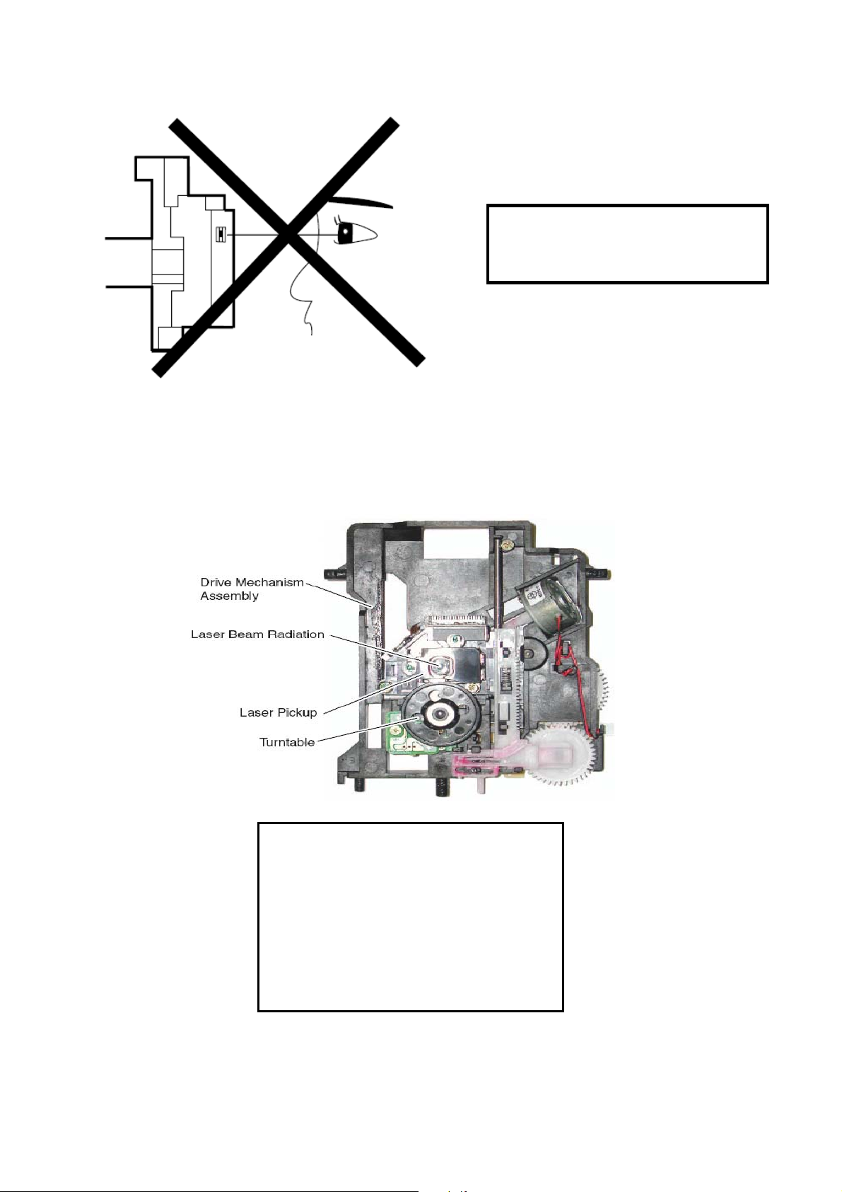
LASER BEAM SAFETY PRECAUTIONS
This DVD player uses a pickup that emits a laser beam.
Do not look directly at the laser beam
coming from the pickup or allow it to
strike against your skin.
The laser beam is emitted from the location shown in the figure. When checking the laser
diode, be sure to keep your eyes at least 30 cm away from the pickup lens when the diode is
turned on. Do not look directly at the laser beam.
CAUTION: Use of controls and adjustments, or doing procedure s o t her than those specified
herein, may result in hazardous radiation exposure.
CAUTION
LASER RADIATION
WHEN OPEN. DO NOT
STARE INTO BEAM.
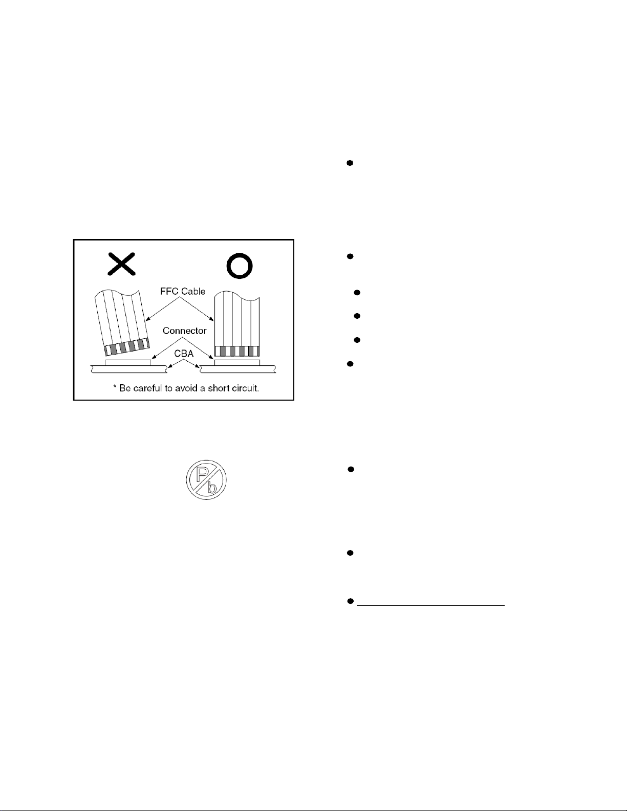
Location: Top of DVD mechanism.
1 - 2
Page 3
STANDARD NOTES FOR SERVICING
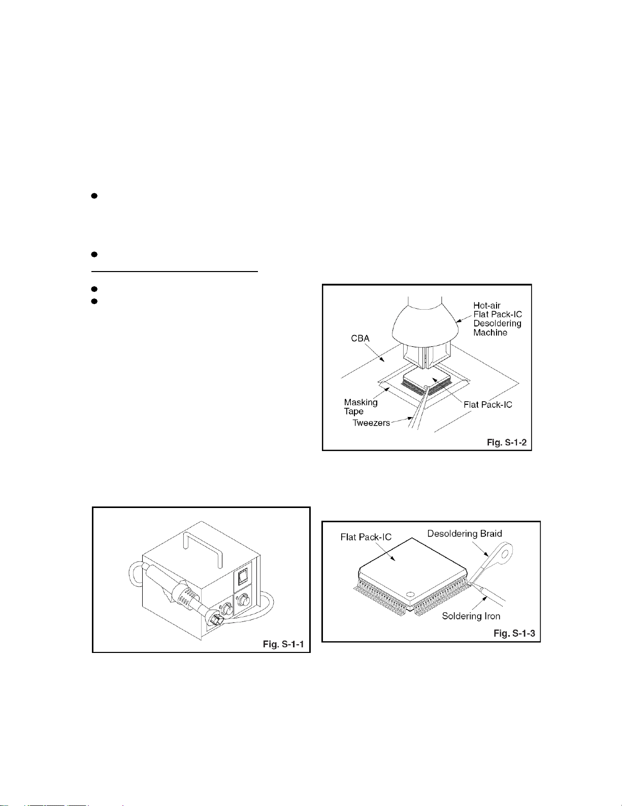
Instructions for Connectors
1. When you connect or disconnect the FFC
(Flexible Foil Connector) cable, be sure to first
disconnect the AC cord.
2. FFC (Flexible Foil Connector) cable should
be inserted parallel into the connector, not at
an angle.
Pb (Lead) Free Solder
When soldering, be sure to use the Pb free
solder.
IDENTIFICATION:
Regardless of special logo (not always
indicated)
One must treat all sets from 1.1.2005
onwards, a
Important note: In fact also products a little
older can also be treated in this way as long as
you avoid mixing solder-alloys (leaded/
lead-free). So best to always use SAC305 and
the higher temperatures belong to this.
Due to lead-free technology some rules have
to be
respected by the workshop during a repair:
ccording next rules.
Use only lead-free solder alloy Philips
SAC305 with order code 0622 149 00106. If
lead-free solder paste is required, please
contact the manufacturer of your
solder-equipment. In general use of solder
paste within workshops should be avoided
because paste is not easy to store and to
handle.
Use only adequate solder tools applicable
for leadfree solder alloy. The solder tool must
be able
To reach at least a solder-temperature of
400°C,
To stabilize the adjusted temperature at
the solder-tip
To exchange solder-tips for different
applications.
Adjust your solder tool so that a temperature
around 360°C - 380°C is reached and
stabilized at the solder joint. Heating-time of
the solder-joint should not exceed ~ 4 sec.
Avoid temperatures above 400°C otherwise
wear-out of tips will rise drastically and
flux-fluid will be destroyed. To avoid wear-out
of tips switch off un-used equipment, or
reduce heat.
Mix of lead-free solder alloy / parts with
leaded solder alloy / parts is possible but
PHILIPS recommends strongly to avoid mixed
solder alloy types (leaded and lead-free). If
one cannot avoid, clean carefully the
solder-joint from old solder alloy and re-solder
with new solder alloy (SAC305).
Use only original spare-parts listed in the
Service-Manuals. Not listed standard-material
(commodities) has to be purchased at external
companies.
Special information for BGA-ICs:
- always use the 12nc-recognizable soldering
temperature profile of the specific BGA (for
desoldering always use highest lead-free
1 - 3
Page 4
temperature profile, in case of doubt)
- lead free BGA-ICs will be delivered in
so-called 'dry-packaging' (sealed pack
including a silica gel pack) to protect the IC
against moisture. After opening, dependent of
MSL-level seen on indicatorlabel in the bag,
the BGA-IC possibly still has to be
baked dry. This will be communicated via
AYS-website.
Do not re-use BGAs at all.
For sets produced before 1.1.2005,
containing leaded soldering-tin and
components, all needed spare-parts will be
available till the end of the service-period. For
repair of such sets nothing changes.
On our website
www.atyourservice.ce.Philips.com
more information to:
BGA-de-/soldering (+ baking inst ructions)
Heating-profiles of BGAs and other ICs
used in Philips-sets.
You will find this and more technical
information within the “magazine”, chapter
“workshop news”.
For additional questions please contact your
local repair-helpdesk.
you find
How to Remove / Install Flat
Pack-IC
1. Removal
With Hot-Air Flat Pack-IC Desoldering
Machine:
1. Prepare the hot-air flat pack-IC desoldering
machine, then apply hot air to the Flat Pack-IC
(about 5 to 6 seconds). (Fig. S-1-1)
be melted). (Fig. S-1-6)
4. Release the flat pack-IC from the CBA using
tweezers. (Fig. S-1-6)
CAUTION:
1. The Flat Pack-IC shape may differ by
models. Use an appropriate hot-air flat
pack-IC desoldering machine, whose shape
matches that of the Flat Pack-IC.
2. Do not supply hot air to the chip parts
around the flat pack-IC for over 6 seconds
because damage to the chip parts may occur.
Put masking tape around the flat pack-IC to
protect other parts from damage. (Fig. S-1-2)
3. The flat pack-IC on the CBA is affixed with
glue, so be careful not to break or damage the
foil of each pin or the solder lands under the IC
when removing it.
With Soldering Iron:
1. Using desoldering braid, remove the solder
from all pins of the flat pack-IC. When you use
solder flux which is applied to all pins of the flat
pack-IC, you can remove it easily. (Fig. S-1-3)
2. Remove the flat pack-IC with tweezers while
applying the hot air.
3. Bottom of the flat pack-IC is fixed with glue
to the CBA; when removing entire flat pack-IC,
first apply soldering iron to center of the flat
pack-IC and heat up. Then remove (glue will
2. Lift each lead of the flat pack-IC upward one
by one, using a sharp pin or wire to which
solder will not adhere (iron wire). When
heating the pins, use a fine tip soldering iron or
a hot air desoldering machine. (Fig. S-1-4)
1 - 4
Page 5
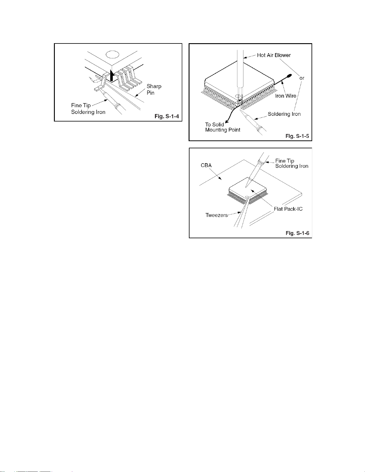
3. Bottom of the flat pack-IC is fixed with glue
to the CBA; when removing entire flat pack-IC,
first apply soldering iron to center of the flat
pack-IC and heat up. Then remove (glue will
be melted). (Fig. S-1-6)
4. Release the flat pack-IC from the CBA using
tweezers. (Fig. S-1-6)
With Iron Wire:
1. Using desoldering braid, remove the solder
from all pins of the flat pack-IC. When you use
solder flux which is applied to all pins of the flat
pack-IC, you can remove it easily. (Fig. S-1-3)
2. Affix the wire to a workbench or solid
mounting point, as shown in Fig. S-1-5.
3. While heating the pins using a fine tip
soldering iron or hot air blower, pull up the wire
as the solder melts so as to lift the IC leads
from the CBA contact pads as shown in
Fig.S-1-5.
4. Bottom of the flat pack-IC is fixed with glue
to the CBA; when removing entire flat pack-IC,
first apply soldering iron to center of the flat
pack-IC and heat up. Then remove (glue will
be melted). (Fig. S-1-6)
5. Release the flat pack-IC from the CBA using
tweezers. (Fig. S-1-6)
Note: When using a soldering iron, care must
be taken to ensure that the flat pack-IC is not
being held by glue. When the flat pack-IC is
removed from the CBA, handle it gently
because it may be damaged if force is applied.
2. Installation
1. Using desoldering braid, remove the solder
from the foil of each pin of the flat pack-IC on
the CBA
so you can install a replacement flat pack-IC
more easily.
2. The “●” mark on the flat pack-IC indicates
pin 1. (See Fig. S-1-7.) Be sure this mark
matches the 1 on the PCB when positioning
for installation. Then presolder the four
corners of the flat pack-IC. (See
Fig. S-1-8.)
3. Solder all pins of the flat pack-IC. Be sure
that none of the pins have solder bridges.
1 - 5
Page 6
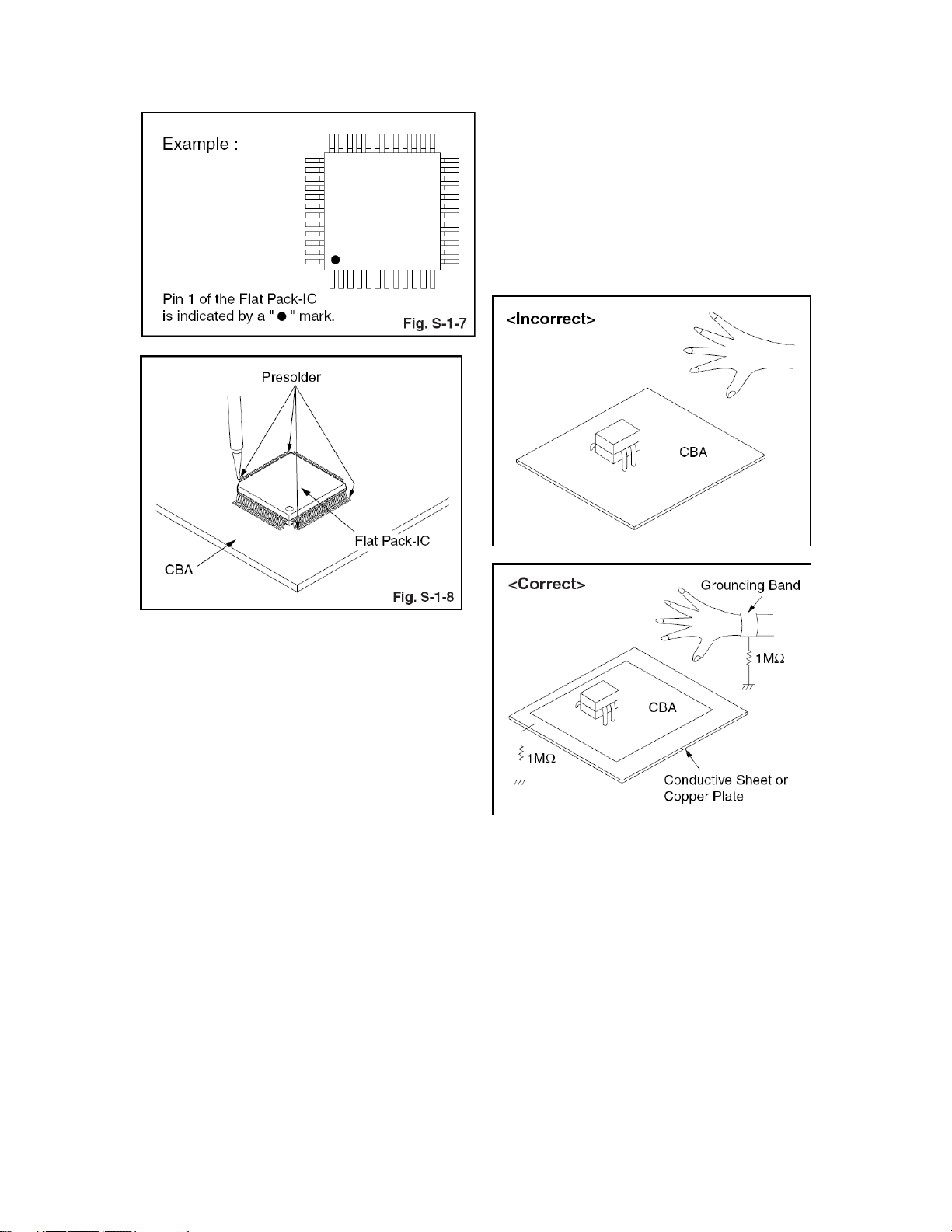
2. Ground for Workbench
Be sure to place a conductive sheet or copper
plate with proper grounding (1 M∧) on the
workbench or other surface, where the
semi-conductors are to be placed. Because
the static electricity charge on clothing will not
escape through the body grounding band, be
careful to avoid contacting semi-conductors
with your clothing.
Instructions for Handling
Semiconductors
Electrostatic breakdown of the
semi-conductors may occur due to a potential
difference caused by electrostatic charge
during unpacking or repair work.
1. Ground for Human Body
Be sure to wear a grounding band (1 M∧) that
is properly grounded to remove any static
electricity that may be charged on the body.
1 - 6
Page 7
Safety and important notice
Warning
• Risk of overheating! Never install the Home
Theater System in a confi ned space. Always
leave a space of at least 4 inches around the
Home Theater System for ventilation. Ensure
curtains or other objects never cover the
ventilation slots on the Home Theater System.
• Never place the Home Theater System,
remote control or batteries near naked fl ames
or other heat sources, including direct sunlight.
• Only use this Home Theater System indoors.
Keep this Home Theater System away from
water, moisture and liquid-fi lled objects.
• Never place this Home Theater System on
other electrical equipment.
• Keep away from this Home Theater System
during lightning storms.
• Where the mains plug or an appliance
coupler is used as the disconnect device,
the disconnect device shall remain readily
operable.
• Visible and invisible laser radiation when open.
Avoid exposure to beam.
Recycle notice
This electronic equipment contains a large
number of materials that can be recycled
or reused if disassembled by a specialized
company. If you are disposing of an old
machine, please take it to a recycling center.
Please observe the local regulations regarding
disposal of packaging materials, exhausted
batteries and old equipment.
Copyright notice
This product incorporates copyright
protection technology that is protected
by method claims of certain U.S. patents
and other intellectual property rights
owned by Macrovision Corporation and
other rights owners. Use of this copyright
protection technology must be authorised
by Macrovision Corporation, and is intended
for home and other limited viewing uses only
unless otherwise authorised by Macrovision
Corporation. Reverse engineering or
disassembly is prohibited.
About Progressive Scan
Consumers should note that not all high
defi nition television sets are fully compatible
with this product and may cause artifacts to
be displayed in the picture. In case of 525
or 625 progressive scan picture problems,
it is recommended that the user switch the
connection to the ‘standard defi nition’ output.
If there are questions regarding our TV set
compatibility with this model 525p and 625p
DVD player, please contact our customer
service center.
1 - 7
Page 8
LOCATION OF PCB BOARDS
LED BOARD
VERSION VARIATION:
Features
Output Power-200W
Voltage(220V-240V)
MP3 Link
Type/Versions
HTS3020
/12/05
HTS3019
Χ
Χ
Χ Χ
SERVICE SCNARIO MATRIX:
Board in used
DECODE board
POWER board
AMP board
LED board
KEY board
Type/Versions
HTS3020
/12/05
Bd Bd
Bd Bd
Bd Bd
Bd Bd
Bd Bd
/12
*Bd=Board Level Repair
/12
Χ
Χ
HTS3019
DECODE BOARD
KEY BOARD
AMP BOARD
POWER BOARD
2 - 1
Page 9
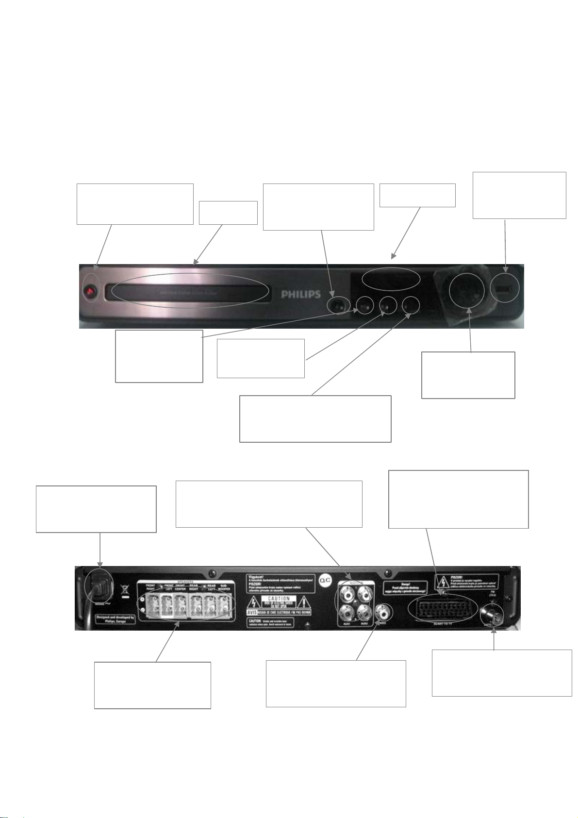
OPERATING CONTROLS AND FUNCTIONS
Front Panel
Standby-On
—
Turns on the player or
switches to standby mode
Play/Pause
—starts or pauses —Stops playback
Back Panel
MAINS~(AC Power cord)
—Connect to a standard
AC outlet
SPEAKERS
—Connect the Speakers
to the matching jacks
playback
Disc Tray
Stop
AUDIO IN
—Connect the audio cables(not supplied)
to the AUDIO IN_AUX1 jacks
Open/Close
—
Opens or closes the disc
compartment.
SOURCE
—
Selects a media to play or listen to
audio from the connected device.
VIDEO
—Connect a composite video
cable to the video jack
USB
Display Panel
VOLUME
Increases or
SCART to TV
—
decreases volume.
—Connects a USB
supported device
— Connect a scart cable(not
supplied) to the SCART to
TV jack
ANTENNA
—Connect the FM antenna to
the FM 75
jack
Ω
2 - 2
Page 10

SPECIFICATIONS
AMPLIFIER
Total output power .................................. 200 W RMS(30%THD)
Frequency Response ..........................…....……….63Hz – 14kHz / ±3 dB
Signal-to-Noise Ratio ..............................................>- 60 dB (A-weighted)
Input Sensitivity
- AUX.………........ ........................................................................500 mV
- SCART TO TV .............
- MP3 LINK .............................................................................. 500 mV
RADIO
Tuning Range ...............................................................FM 87.5-108 MHz
.......................................................................................................(50kHz)
............................................................................................26 dB Quieting
Sensitivity..... ...........................................................................FM 22 dBf,
IF Rejection Ratio .....................................................................FM 50 dB
Signal-to-Noise Ratio ................................................................FM 30 dB
Harmonic Distortion ..................................................................... FM 3%
Frequency Response ..................................... FM 180 Hz
Stereo Separation ......................................................... FM 26 dB (1 kHz)
Stereo Threshold .....................................................................FM 23.5 dB
DISC
Laser Type ......................................................... ........…...Semiconductor
Disc Diametre .........................................................................12cm / 8cm
Video Decoding ...............................................MPEG-1 / MPEG-2 /DivX
................................................................................................ / DivX Ultra
Video DAC ......................................................................12 Bits,108MHz
Signal System ........................................................................PAL / NTSC
Video S/N ......................................................................................... 56 dB
Audio DAC..........................................................................
Frequency Response ........................................... 4 Hz–20 kHz (44.1 kHz)
.............................................................................. ..4 Hz–22 kHz (48 kHz)
..................................................................................4 Hz–44 kHz (96 kHz)
PCM .......................................................................................... IEC 60958
Dolby Digital ......................................................... IEC 60958, IEC 61937
........................................................... 500 mV
–10 kHz / ±3 dB
............. 24b
its/96KHz
SPEAKERS
System .................................................... ...... Full range satellite
Speaker impedance ............................8 ohm(centre),4 ohm(Front/Rear)
Speaker drivers .................................................... .3” full range speaker
Frequency response .....................................................150 Hz – 20 kHz
Dimensions:
-Center……………………………………….....100 x 100x 75 (mm)
-Front/Rear..……………………….………….. 100 x 100x 75 (mm)
.................................................................................................(w x h x d)
Weight:
-Center……………………………………………….....…..…0.38kg
-Front/Rear……………………………………......…….0.38 kg/each
USB
Compatibility ................................ ... ............................................... USB
Class support ........................................................ UMS(USB Mass storage Class)
File system...........................................................................FAT12,FAT16,FAT32
SUBWOOFER
Impedance .....................................................................................8 ohm
Speaker drivers ................................ .................... 165mm (6.5”) woofer
Frequency response .........................................................45Hz – 150 Hz
Dimensions .......................................
..................................................................................................(w x h x d)
Weight ............................................................................................3.54kg
...............122.6x 30
9.5 x 369 (mm)
Laser specification
Type.................................................
Wave length...................................... 645-665nm (DVD) 770-800nm(CD)
Output power ................................................................6Mw(DVD) 7Mw(VCD/CD)
Beam divergence....................................................................... 60 degrees
...........Semiconductor la
ser GaAlAs(CD)
MAIN UNIT
Power Supply......………………...........……................220 - 240 V~50Hz
Standby power consumption................................................................<1W
Power Consumption ............................................................................50 W
Dimensions ................................................................ 360 x 48 x 332 (mm)
......................................................................................................(w x h x d)
Weight ...............................................................................................2.64 kg
3 - 1
Page 11
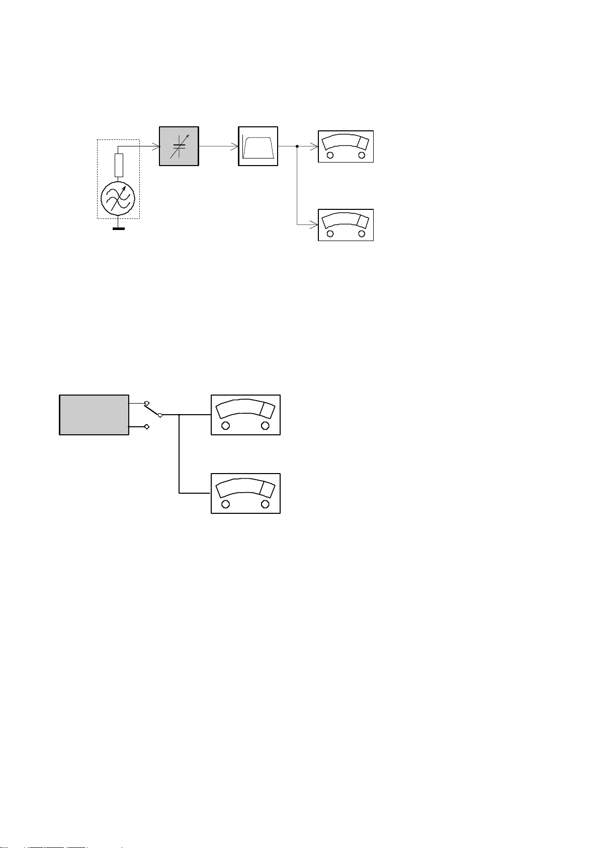
MEASUREMENT SETUP
Tuner FM
DUT
RF Generator
e.g. PM5326
Ri=75Ω
Bandpass
20Hz-15kHz
e.g. 7122 707 48001
LF Voltmeter
e.g. PM2534
S/N and distortion meter
e.g. Sound Technology ST1700B
Use a bandpass filter to eliminate hum (50Hz, 100Hz) and disturbance from the pilottone (19kHz, 38kHz).
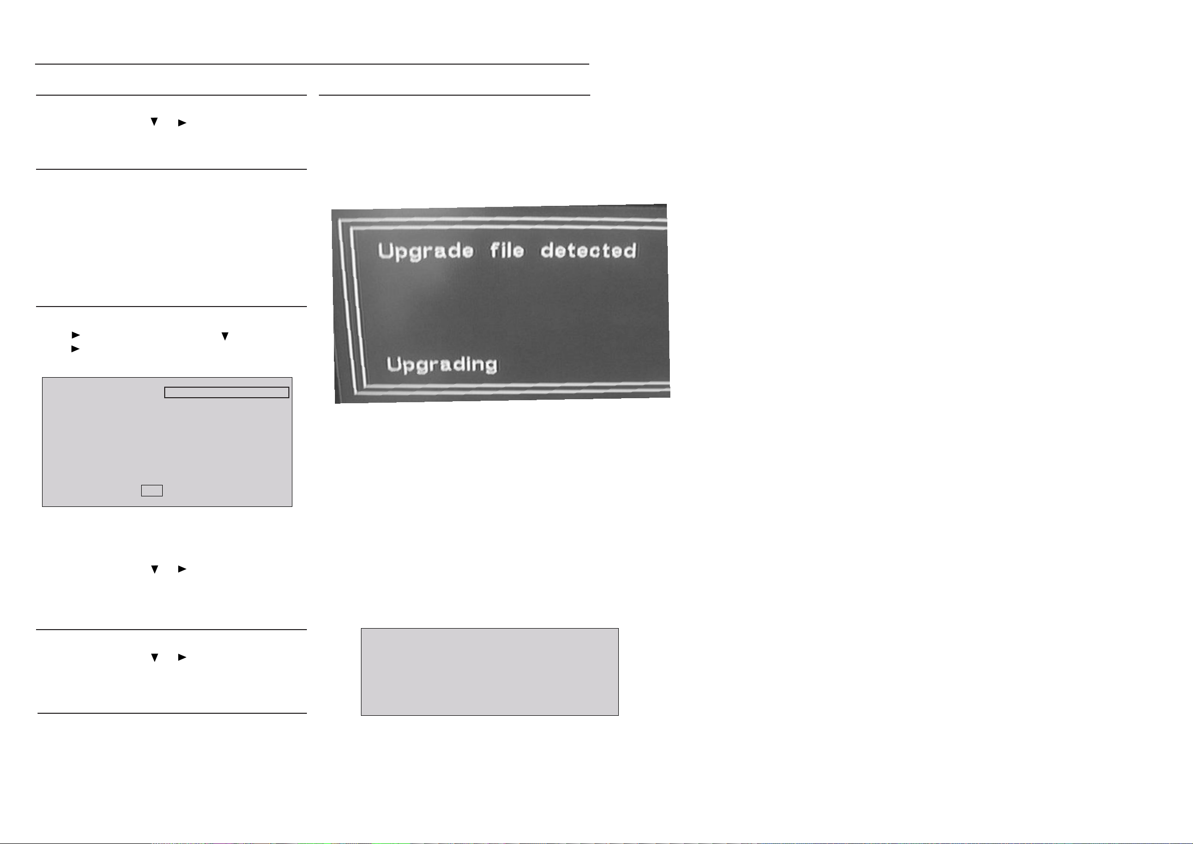
CD
Use Audio Signal Disc
(replaces test disc 3)
DUT
L
R
SBC429 4822 397 30184
S/N and distortion meter
e.g. Sound Technology ST1700B
LEVEL METER
e.g. Sennheiser UPM550
with FF-filter
3 - 2
Page 12
System , Region Code , etc. Setting Produre
1)System Reset
a) Press “SETUP“ button on RC,TV will show setup menu
b) Select the menu using the and
c) Go preference page to do system reset
2)Region Code Change
a) In open model, press”9” “9“ “9“ “9“ on R/C,then input desired
number to change region code :
1 USA
2 EU
3 AP
4 Australia ,NZ , Latam
5 Russia , INDIA
6 CHINA
3)Version Control Change
a) In open model, press “1“ “5“ “9“ on RC
b) Press and select version you want using
c) Press and “ok” button to con rm
d) TV will show message as below:
on RC
7) Upgrading new sofeware
a) Copy “sofeware les” into a CD-R or USB flash drive.
b) Insert the CD-R disc or USB flash drive.
c) Press DISC or USB, the system will identify the update file autometically.
d) VFD will show
* the system will switch off to standby automatically after update is complete.
e) OSD will show:
“Updating“ until update is complete.
Current model
Ver19.01.2M _090213_0 Region
Servo: AE.56.00.00
8032: 05.00.04.06 RISC: 05.02.00.24
IF current model does not match you set use down arrow
key on the remote to change
OK
4)Password Change
a) Press “SETUP“ button on R/C,TV will show setup menu
b) Select the menu using the and on RC
c) Go preference page select “password“ to change
* 136900 is default password supplied.
5)Check on the Sofeware Version
a) Press “SETUP“ button on R/C,TV will show setup menu
b) Select the menu using the and on RC
c) Go preference page select “Version Info“.
TV will show the version on screen.
6)Trade model
HTS3020/12
&
HTS3019/12
/05
: 6
CAUTION!
This information is confi dential and may not be
distributed.Only a qualifi ed se rvice person should
reprogram the Region Code.
a) Press “Open/Close “ button on RC
b) Press “2” “5” “9” on R/C,VFD will display “TRA ON “ or “TRA
OFF“
3 - 3
Page 13
3 - 4
Page 14
y
y
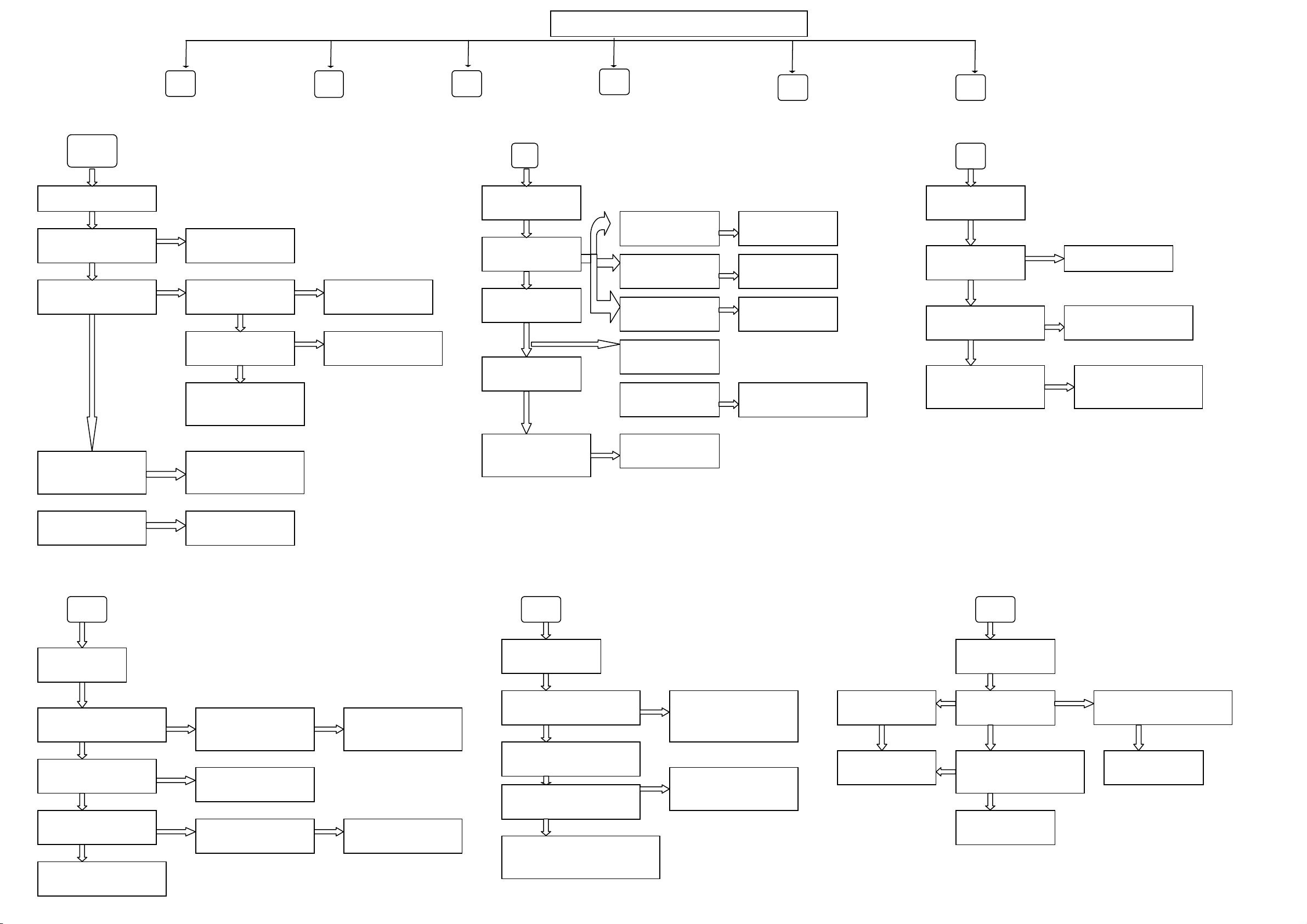
MAIN UNIT REPAIR CHART
AII Function NO
Working
A
AII Function NO Working
Check AII System, AII Coble
is Loose or bad: INT
not
Panel stand LED show
working or Not
working
A
B
Power supply NO
working
YES
RE-insert and fix the
cable
not bad
Check Back Power PCB
F901 Bad cause Damage
Check Con902 pin1
+5V affirm Correct
no
Change F901
Repair between T901
Circuit
Check control PCB
IC901 and their conjoint
Part
C
ALL Function NO
Sound
Power supply NO
Working
ALL voltage No
ALL voltage No
output
output
Check F901 Bad
Cause Damage
Check ic901
Working Or Not
not
B
YES
YES
not
YES
D
DVD Audio NO
Sound
+27V Voltage No
Output
+5V Voltage No
Output
+/-12v Voltage No
Output
Repair The Part
Check Q901 and its
conn circuit
E
Aux/TV in NO
Sound
Check D916 and its
conjoint part
Check D911 D912
and its conjoint part
Check D908 D910
and its conjoint part
not
Check Repair D905 and
conn circuit
F
Tuner NO Sound
C
ALL Function No
Sound
ok
Check cn801 vcc
Voltage=27V
ok
Check IC801A IC801B
Voltage correct is ok
ok
Check ic801a ic801b pin
23 Voltage is 3.3v
not
See Contents B
not
Check repair D916 and its
conjoint part
not
Check repair Q804=3.3V
and its conjoint part
YES
Repair The part
not
Check between U102
PIN162 163 164 and their
cojoint part
not
not
Check repair Between
L131=5V and their conjoint
part
Check D101
Voltage=10.1v
not
Check Q101 and
their conjoint part
F
Tuner NO Sound
not
Check cn111
pin9=9V
es not
Check IC112 PIN4=-12V
PIN8=+12V and other
conjoint part
not
According AUX/TV
REPAIR
es
Check u102 PIN198 199 200
and pin201 other conjoint part
Alternate tuner
Check servo pcb
Check U100 PIN2 1V8
Check U101 PIN2 3V3
Check CON903 PIN2
M5V affirm Correct
D
DVD Audio not
sound
Check open/close and disc
change working or not
ok
Check cn102 to DVD
loader loose or bad not
not
Hae picture output Yes
or No
ok
Check IC u102 AND
ok
Check Repair
U102,U104,U105,U106
Circuit
Check Switch power
Supply Circuit
not
Check cn102 cn101and
cn105 to dvd loader,
cable loose or bad int
ok
Re-insert and fix the
cable
not
Check ic804 their
conjoint part
not
Check U102 and their
cojoint part
ok
Check repair Between
ic801
Check power
Transformer Working
Or Not
E
Aux/TV in No
Sound
Check U107 U108 and its
conjoint part offirm working
Check U107 U108 PIN7=-5.1
pin16=+5V
Check U109 and its conjoint
part offirm working
not
Check U102 PIN109,210,211and
214 its conjoint part
con100 its conjoint part
3 - 5
Page 15

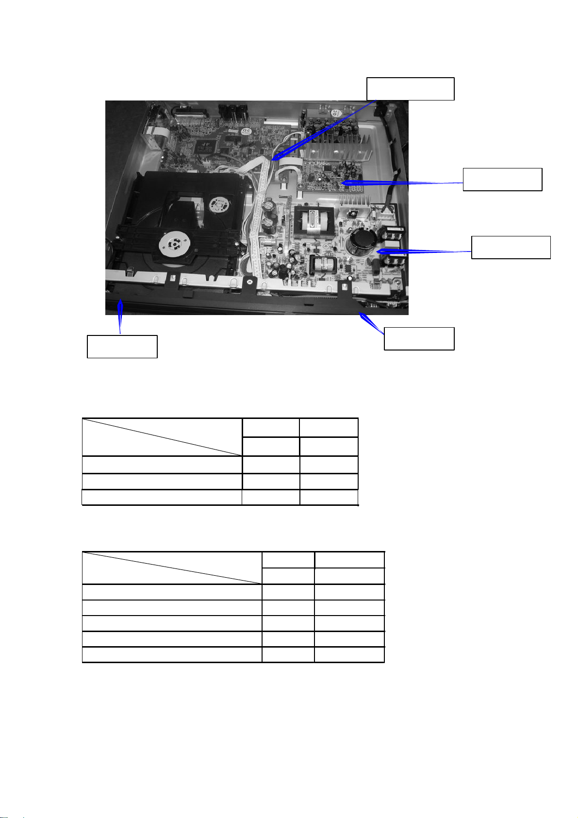
DISASSEMBLY INSTRUCTIONS
1. Disassembly Flowchart
This flowchart indicates the disassembly steps to gain access to item(s) to be serviced. When
reassembling, follow the steps in reverse order. Bend, route, and dress the cables as they were
originally.
Top Case
Loader
Dismantling of top case
2.
2-1. Ensure no disc in the tray and keep tray close, turn off the DVD player and then disconnect the mains supply.
Loosen 6 screws“A” as shown in figure 2-1.
Decode
Board
Led
Board
Front
Panel
A
Figure 2-1.
Power
Board
Key
Board
Amplifier
Board
Tuner
4 - 1
Page 16

2-2. Take off the top case as shown in figure 2-2.
OPEN
Figure 2-2.
3. Dismantling of
led+key board
3-1. Loosen 4 screws “B” as shown in figure 3-1.
B
Figure 3-1
4 - 2
Page 17

3-2. Release the lock “C” at the same time as shown figure 3-2.
PUSH PUSH PUSH
PUSH
C
3-3. Loosen 5 screws “D” as shown in figure 3-3.
4. Dismantling of loader
4-1. Loosen 4 screws “E” as shown in figure 4-1.
PUSH
Figure 3-2
D
Figure 3-3
E
Figure 4-1
4 - 3
Figure 4--1
4 - 3
Page 18

G
5. Dismantling of dec ode board
5-1. Loosen 4 screws as shown in figure 5-1.
6. Dismantling of power board
F
Figure 5-1
6-1. Loosen 4 screws “G” as shown in figure 6-1.
Figure 6-1
4 - 4
Page 19

7. Dismantling of amplifier board
7-1. Loosen 4 screw “H” as shown in figure 7-1
H
8. Dismantling of tuner
8-1. Loosen 1 screws “I” as shown in figure 8-1.
I
Figure 7-1.
Figure 8-1.
9. Dismantling of L ed board
9-1. Loosen 2 screws “J” as shown in figure 9-1.
J
Figure 9-1.
4 - 5
Page 20

FM
C1
C2
C3
C4
C5
C6C7C8
C9
C10
C11
C12
C13
BLOCK WIRING DIAGRAM
Kwang sung KST-MT
or Panasonic TM10 V2
TUNED
Lch
Stereo
RchNCVCC
SDA
SCL
Port Select
GND/PD
FBARFCD/DVD_SWDCT-T+F+F-
GND
CD-LD
VR-DVD
VR-CDNCE
VCC
VC(VREF)
Traverse & Loader
SANYO DV38 HD868 & ASA8829
HFM
MD
DVD-LD
NC
SLED-
SLED+
HOMESW
GND
LOAD-
LOAD+
INSW
GND
OUT_SW
GND-LD
SP+
SP-
Main (MPEG/Decode)Board
(/37option)
Port Select
SCL
SDA
TUNED
Lch
Stereo
Rch
NC
VCC
GND
GND-LD
DVD-LD
NC
HFM
MD
CD-LD
VR-DVD
VR-CD
NC
E
VCC
VC(VREF)
GND/PD
F
B
A
RF
CD/DVD_SW
D
C
TT+
F+
F-
SLEDSLED+
HOMESW
GND
SP+
SP-
LOADLOAD+
INSW
GND
OUT_SW
Red(YUV and SCART) for EUP/UK
AUX1(TV)) SCART OUT
iPOD dock
4558
4558
SAA6581T etc.
RDS(option)
L
Switch
ADC WM8782
or CS5340
etc.
R
MIC IN
Scart in(L/R IN)
or AUX2
MOTO Driver
AM5888S
etc.
RF
3.3V
YPb/Cb
CVBS
Bufer
Video Encoder
MPEG IC
MTK1389HD
16/32Mbit Flash
MCU(option)
USB
GND
MIC SW
MIC MIC
karaoke
5VDPDN
5VDPDN
GND
MIC SW
USB
USB/karaoke Board
05/37/12 without karaoke
Blue(YUV or SCART) for EUP/UK
Pr/Cr
L/R IN
RGB
CVBS L/R
PI5V330
64Mbit SDRAM
DC to DC5V3.3V 1.8VDC to DC5V3.3V 1.8V
other
CS/STB
CLK
GND
IR
DATA
I2C-CLK
GND
GND
GND
MIC SW
SCART SW
I2C-Data
ST (TI option) SOLUTION AMP
+12V
GND
-12V
GND
+5V
GND
VOL-
GND
VOL+
P-MUTE
LJ-L
LJ-R
MUTE
GND
POWER
TSDA0
TSD1
TSD2
GND
ALRCK
ABCK
RES
GND
SCL
SDA
A-MCLK
GND
26V 26V GNDGND
+12V
GND
-12V
GND
+5V
GND
AC3.3V
AC3.3V
-24V
GND
B5V
STB
RL
26V 26V GNDGND
Rectifier LC filiter
TRANSISTOR2
MOSFET
PWM
FSQ110
PSU Board
AMP EASY FIT JACK
LC
LSRC
STA518 STA518
L/R/SL/SR:4 ohm C/SW:8 ohm
TRANSISTOR1
STA309A/B
ST AMP Board
MOSFET
PWM
FSCQ1265RT
SW
SL
/05/12/37/55 Fixed
/98/94/51 Detach
AC 110-240V,50/60Hz or 230V+-15%(for EUP.)
AC Line
LED
KEY
STB
Switch board
GND
LED
STB-GND
STB
Panel (control)Board
VFD dirver ic
V63111 (or PT6311)
SCART SW
IR
I2C-Data
GND
I2C-CLK
GND
MIC SW
VFD
AOTOM 20070-1A04(D812C)
or SAMSUNG: HNV-08SS77
5 - 1
GND
B5V
STB
VOL-
GND
CLK
DATA
CS/STB
VOL+
IR
4 Keys
-24V
AC3.3V
AC3.3V
VOL.
Page 21

AMPLIF IER BOARD
INTERNAL IC DIAGRAM - STA309A
SA SCL SDA MVO
TABLE OF CONTENTS
Internal IC Diagram ........................................................................... 6-1
Sch ematic Diagram (part one)
Sch ematic Diagram (part two)
Sch ematic Diagram (part th ree)
Top View
Bottom View
........................................................................................... 6-5
...................................................................................... 6-6
......................................................... 6-2
......................................................... 6-3
....................................................... 6-4
LRCKI
BICKI
SDI12
SDI34
SDI56
SKI78
PLLB
SERIAL
DATA
IN
CHANNEL
MAPPING
PLL
XTI
VARIABLE
OVERSAMPLING
SYSTEM TIMING
CKOUT
2
I C
SYSTEM
CONTROL
POWER
DOWN
PWDN EAPD
TREBLE
BASS EQ
(BIQUADS)
OVERSAMPING
VOLUME
LIMITING
VARIABLE
DOWNSAMPLING
DDX
SERIAL
DATA
OUT
OUT1A/B
OUT2A/B
OUT3A/B
OUT4A/B
OUT5A/B
OUT6A/B
OUT7A/B
OUT8A/B
LRCKO
BICKO
SDO12
SDO34
SDO56
SDO78
6 - 1
6 - 1
Page 22

AMPLIFIER BOARD SCHEMATIC DIAGRAM 1/3
6 - 2
Page 23

AMPLIFIER BOARD SCHEMATIC DIAGRAM 2/3
6 - 3
Page 24

AMPLIFIER BOARD SCHEMATIC DIAGRAM 3/3
6 - 4
Page 25

AMPLIFIER BOARD TOP VIEW
6 - 5
Page 26

AMPLIFIER BOARD BOTTOM VIEW
6 - 6
Page 27

LED KEY BOARD
TABLE OF CONTENTS
FTD Display Pin Assignment . . . . . . . . . . . . . . ............................................... 7 -1
Sch ematic Diagram
Top & Bottom View
&
........................................................................... 7 -2
............................................................................ 7 -3
FTD DISPLAY PIN ASSIGNMENT
7 - 1
7 - 1
Page 28

5
LED+KEY BOARD SCHEMATIC DIAGRAM
U300
R527
10K/ NC
VOL
D D
3
2
1
3 HEADER
R510 10K
R511 10K
DWDW
DWDW
R526
10K/ NC
UP
CB506
150pF
CB533
ESD
CB507
150pF
CB532
ESD
F2
F2
26
27
28
F2 F1
VCC
4/2.0 HEADER
J500
SW5
3 4
1 2
SPOWER1 KEY
C C
4/2.0 HEADER
B B
1=2 3=4
J506
POWER/STB
STB
LED
4
GND
3
POWER/STB
2
STB
1
CB522
NC ESD
1
2
3
4
D511
LED DIP2.54
CB523
NC ESD
VCC
CB524
VCC
R538
R523 220
CB501 150pF
ESD
CB502 150pF
R502 22K
PSW
10K/ NC
Y505
455KHz
R501 2K2
40
41
42
43
44
45
46
47
48
49
50
51
52
R503 10K
CB539
ESD
+
47uF/10V
CE501
3/2.5 HEADER
CB519
R528100
R529100
CB517
0.1uF /NC
R530100
CB530
ESD/NC
R531100
CB528
ESD/NC
1
2
3
J515/ MP3
1
2
3
J508/ MIC
K_L0
3
2
1
J510
ESD/NC
J511
A A
3
2
1
3/2.0 HEADER
CB529
CB531
K_L1
ESD/NC
K_R0
CB516
0.1uF /NC
K_R1
CB518
0.1uF /NC
4
39383736353433323130292827
U520
GR6
GR7
GR5
GR4
GR3
GR2
GR1
VDD
VFD CONTROLLER
PSW
GPIO4
GPIO3
GPIO2
GPIO1
GND
OSC2
RESET
OSC1
1
D504
D502
D503
D501
1N4148
1N4148
1N4148/NC
1N4148/NC
P12
P13
P14
P15
P168G7G6G5G4G3G2G1G
VCC-24V
VEE
GR8
VDD
SG20/GR9
SG19/GR10
V63111
PIN/OUT
SDA
ROMETO
MODE
SCL
5689101112
432
7
IR_V6111
R507 4.7K
R515 4.7K
VCC
P11
SG18/GR11
SCK
R508 4.7K
P10
SG17/GR12
SG16/GR13
STBK1K2
R509 1K
R513 1K
SG15/GR14
R514 1K
SG14/GR15
SG4/KS4
SG3/KS3
SG2/KS2
SG1/KS1
K3
SG12
SG11
SG13/GR16
SG10
SG9
SG8
SG7
SG6
SG5
VDD
K4
V63111/SMD
13
PT6-52-1
R512 1K
POWER/STB
P1P2P3P4P5P6P7P8P9
26
25
24
23
22
21
20
19
18
17
16
15
14
CB538
0.1uF
F1
F1
12345678910111213141516171819202122232425
CB521
OPEN/CLOSE KEY
STOP KEY
SOURCE KEY
VFDA
200780-1A0
VCC
0.1uF
STB
SW1
3 4
1 2
1=2 3=4
SW3
3 4
1 2
1=2 3=4
SW4
3 4
1 2
1=2 3=4
3
CB536
0.1uF
D509
D507
1N4148
1N4148
SW2
3 4
1 2
1=2 3=4
D508
D505
1N4148
PLAY/PAUSE KEY
1N4148
PSW
D50
1N4148
R519 0
VCC
IR_V6111
10K
CE5xx
10uF/16V
CB515
22pF
CB50330pF
R516
R520 4.7K
R521 33
CB50530pF
CB50430pF
USB
+
VCC
3
UP
DW
R518
4.7K
4
3
2
1
2
2
Reset
IMP810
1
IR
R524 0
R525 0
Q501
CB537
ESD
R534 33
R535 33
R536 0
VCC
IR
GND
VFD_CLK
VFD_STB
VFD_DATA
U_P
DONW
BT-14S
CE506
+
10uF/10v
IR501
R505 10K/NC
IR
CB520
0.1uF
STB ON/OFF
R540 0R
CB514
0.1uF
J505
7 HEADER
1
2
3
4
5
6
7
8
123
CB525
ESD
1/0
+
CB526
ESD
CB535
0.1uF
CE502
10uF/10V
UB
UB
CB527
ESD/NC
ON/OFF
UP
+5V
R517 10
CB513
0.1uF
1
J512
GND
1
2
3
4
4 HEADER
VCC
GND
-24V
F2
F1
R541 NC 0
R537 NC 0
R539 NC 0
VCC
J507
1
2
3
4
5
6
6 HEADER
0.1uF /NC
5
4
3
2
1
7 - 2
Page 29

LED BOARD TOP VIEW
LED+KEY BOARD TOP/BOTTOM VIEW
KEY BOARD TOP VIEW
LED BOARD BOTTOM VIEW
KEY BOARD BOTTOM VIEW
7 - 3
Page 30

DECODE BOARD
TABLE OF CONTENTS
Internal IC Diagram
Sch ematic Diagram
Sch ematic Diagram
Sch ematic Diagram
Sch ematic Diagram
Sch ematic Diagram
Sch ematic Diagram
Top View
....................................................................................... 8 -8
Bottom View
(part one)
(part two)
(part th ree)
(part f our)
(part f iv e)
(part s ix )
.................................................................................. 8 -9
.................................................................... 8 -1
......................................................8 -2
...................................................... 8 -3
..................................................... 8 -4
..................................................... 8 -5
..................................................... 8 -6
..................................................... 8 -7
INTERNAL IC DIAGRAM - MT1389HD
DVD
PUH
Module
Motor
Drive
RASH
ROM
DRAM
RF Amplifier
Servo IO
Spindle
Control
Memory
Controller
System Parser
CPPM/CPRM
DRM
Audio
DSP
Debug
Port
Servo
Processor
108MHz
TV Encoder
De-
Interlacer
Video
Processor
MPEG-1/2 MPEG4 ASP
JPEG Video Decoder
Audio
output
Audio
DAC
Video DAC
PCM
CVBS,Y/C
CVBS,Y/C
Component
Component
Vide
Video
o
digital video
5.1ch Audio
Analog Audio
Output
8 - 1
GPIO
IR/VFD
System
CPU
32-bit
RISC
SDPIF
8 - 1
Page 31

5
DECODE BOARD SCHEMATIC DIAGRAM 1/6
YUV[3..6]
YUV[3..6][2]
MUTE_DAC
MUTE_DAC[2]
FS0
FS0[2]
FS1
FS1[2]
RGB_SWITCH[2]
4 4
SCART_L_IN[5]
SCART_R_IN[5]
RGB_SWITCH
SCART_L
SCART_L[5]
SCART_R
SCART_R[5]
A_MUTE
A_MUTE[5]
AVCC
AVCC[1,2,5]
+12V
+12V[1,5,6]
DV33
DV33[1,2,3,5,6]
+5V
+5V[1,2]
SCART_L_IN
SCART_R_IN
L1541.8uH
YUV4
C191
R298
75,1%
47P
L1561.8uH
YUV5 B/U
R299
C193
75,1%
47P
L1571.8uH
YUV6 R/V
R304
C195
75,1%
47P
2
C192
120P
C194
120P
C196
120P
1
1
1
DIODE SMD BAV99
3
2
DIODE SMD BAV99
3
2
DIODE SMD BAV99
3
G/Y
D107
5V_VIDEO
D108
5V_VIDEO
D109
5V_VIDEO
Low Impedance Mode
3 3
R313 10k
C201
3300pF
3 2
C204
1
1
Q121
2N3906
1
R326 470
R312 510
R314 470
Q118
2N3904
3 2
+5V
32
Q120
2N3906
D113 1N4148
32
Q117
1
2N3906
R318
100
A_MUTE
+5V
D112
5V1
DV33
MUTE_DAC
+12V
R322
2.2k
R324 0
+5V
R316 10K
R317 1k
R325 470
+
220uF/16V
MUTE_Circuit
R327
+12V
FS0
FS1
R330
2.2k
DV33
RGB_SWITCH
680
Q122
1
2N3904
3 2
R332
33
R333
4.7K
SCART CONTROL
R328
1k
R334 2.2k
Q126
2N3906
3 2
R331
2.2k
1
2 2
1 1
1
RGB/CVBS#
CB171
0.1u
3 2
ASPECT
R329
75
Q123
2N3904
4
mark:**
YUV3
R319
75,1%
R320
91R,1%
RGB_SWITCH
G_OUT
Y_OUT
G/Y
B_OUT
U_OUT
B/U
CVBS
RGB_SWITCH: 0--->RGB,
1--->CVBS/YUV
RGB/YUV Switch
IN Dir
L R,G,B
H Y,U,V
1
IN
2
S1A
3
S2A
4
DA
5
S1B
6
S2B
7
DB
8 9
GND DC
NC PI5V330W
R300 NC(0)
R301 NC(0)
R302 NC(0)
R303 NC(0)
R305 NC(0)
B/U
R306 NC(0)
R307 NC(0)
CVBS
R308 NC(0)
L162
22uF/16v
0.22uH
C203
C202
22pF
22pF
FS1
FS0
PIN157
PIN158
0
0
01
10
11
3
Q119
1
2N3904
3 2
R323
75 1%
5V_VIDEO
CB168
0.1u
CB170
0.1uF
2
1
& SCART_CVBS need output,
U113
16
VCC
15
/EN
CVBS_SCART
14
S1D
CVBSO
13
S2D
CVBS
12
DD
R_OUT
11
S1C
V_OUT
10
S2C
R/V
G_OUTG/Y
Y_OUT
R_OUTR/V
V_OUT
B_OUT
U_OUT
CVBS_SCART
CVBSO
5V_VIDEO
R315
3.3K
CE127
+
R321
3.3K
Only when both signal CVBSO
then the parts mark “**” will need to be added.
MT1389
4:3 / USB
16:9
STB / AUX IN / MP3 IN / SCART IN / FM IN
CVBSO
D111
NC DIODE SMD BAV99
3
5V_VIDEO
AVCC
2
C
B
13
3906
L155
FB
E
R342 NC 0.1uF
CE133
2
5V_VIDEO
CB167
+
CE125
0.1uF
22uF/10v
L158 FB
CVBSO
ZD106
1
3
5
7
9
11
13
15
17
19
21
L159 FB
L160 FB
L161 FB
CN112
AR
AL
BGND
VB
SWITCH
GGND
CLKOUT
G
RGND
DATA_GND
R
VGND
BLNK_GND
CVBS
SHIELD
AGND
DATA
BLNK
AIR
VIN
AIL
C197 15p
C198 15p
C199 15p
C200 15p
2
4
6
8
10
12
14
16
18
20
C206 47p
C207 47p
C210 47p
C213 47p
ESD0603/SMD
V_OUT
ZD107
ESD0603/SMD
Y_OUT
ZD108ESD0603/SMD
ZD109ESD0603/SMD
U_OUT
220uF/16v
+
ZD111
ESD0603/SMD
C205 15p
L163 FB
SCART_R
L165 FB
SCART_L
ESD0603/SMD
B_OUT
G_OUT
R_OUT
CVBS_SCART
ZD112
L167 FB
L169 FB
L170 FB
L172 FB
C208 15p
C209 15p
C211 15p
C212 15p
C214 15p
1
JR1
1
2
3
4
5
6
AV-RCA3.5
ZD110
ESD0603/SMD
L164 FB
SCART_R_IN
ZD113 ESD0603/SMD
SCART_L_IN
L166 FB
L168 FB
L171 FB
ASPECT
RGB/CVBS#
SCART CONNECTOR
RGB_SWITCH#: 1-3V RGB, 0-0.4V
CVBS
A_MUTE
A_MUTE
Q125
NC 2N3904
SCART_L
Q124
NC 2N3904
1
1
3 2
SCART_R
3 2
Amute
R340
1k
R339
1k
8 - 2
Page 32

5
DECODE BOARD SCHEMATIC DIAGRAM 2/6
4
3
2
1
TU_L
TU_R
C182
1000P
C190
1000P
TUNER_ON
TUNED
STERED
I2C_CLK
I2C_DAT
R290
13K
R296
13K
R283
68K
C181 47P
R293
68K
TUNE_L
TUNE_R
+9V
DV33
+12V
-12V
TUNER_VCC
Q115
2N3904
Q114
8550
1
R280
3 2
+
CB166
EC129
0.1u
47U/16v
-12V
-
U112A
2
3
6
5
+
8 4
-
+
8 4
1
NJM4558
+12V
-12V
U112B
7
NJM4558
+12V
EC131
10u
+
EC132
10u
+
R284
8.2K
R294
8.2K
TUNE_L
R291
NC 15K
TUNE_R
R297
NC 15K
+9V
32
+
EC130
100U/16v
DV33
1K
R282 4.7K
1
R281
10K
TUNER_ON
I2C_CLK
I2C_DAT
TUNED
TU_L
STERED
TU_R
TUNER_VCC
R28510K
DV33
R286
10K
R28710K
R288
10K
L147 FB
L148 FB
L149 FB
L150 FB
L151 FB
L152 FBC183 47P
L153 FB
C184
33P
C185
33P
C186
33P
C187
33P
NC
R292
C188
33P
PORT_SEL
C189
33P
1
2
3
4
5
6
7
8
9
10
TUNER PORT KST-6A
CN111
TUNE_L [5]
TUNE_R [5]
+9V [1]
DV33 [1,2,3,5,7]
+12V [1,5,7]
-12V [1,5]
TUNER_ON[2]
TUNED[2]
STERED[2]
I2C_CLK[2]
I2C_DAT[2]
R289
10K
R295
10K
5
8 - 3
4
3
2
1
Page 33

5
DECODE BOARD SCHEMATIC DIAGRAM 3/6
U107
13 3
AUIN1_L
IPOD_L_A
TUNE_L
AUIN2_L
AUIN_SL0
AUIN_SL1
AUIN_SL2 AUIN_SL2
D D
VEE_4051
D102
EC113
5V1
+
47UF/10v
1 2
R205 10K
M1
C C
B B
A A
R208 10K/NC
R210 10K
M0
R212 10K/NC
AD_INL
R213 100K
R214 100K
R216 100K
AD_INR
R217 100K
R227 4.7K
ADRST#
R228 10K
R229 10K/NC
ADC_DATA
R235 33
ACLK ADC_ACLK
AMDAT ADC_DATA
R239 56
R242 56
ALRCK
ABCK ADC_ABCK
R243 56
CN107
1
2
3
MP3 IN
CN110
1
2
3
4
5
6
7
8
9
IPOD
X0 X
14
X1
15
X2
12
X3
1
X4
5
X5ENVEE
2
X6
4
X7
11
A
10
B
9
C
6
74HC4051
1 2
CB158
CB157
0.1u
0.1u
L135 FB
L136 FB
L141 FB
L142 FB
L143 FB
L144 FB
L145 FB
L146 FB
C179 100p
C178 100p
VCC
GND
R195
470
ADC_VL
ADC_VL
VCCVA
VCCVA
DV33
DV33
ADC_ALRCK
C169 100P
AVCC
16
7
8
-12V
R248 NC 1.2k
R275 100
ESD0603/SMD/NC
R173 680
R177 100K
VCC_4051
VEE_4051 VCC_4051
EC114
12
+
D103
5V1
ADC_VL VCCVA
C170 100P
R249 NC 1.2k
R264 4.7k
R266 4.7k
R267 4.7k
R269 100
R274 100
ZD101
CB159
47UF/10v
0.1u
M0
ADC_ACLK
ADC_VL
ADC_DATA
ADC_VD
ADC_ABCK
ADC_ALRCK
R215
VCCVA ADC_VD
5.1
L131 FB
CB164
C168
0.1uF
1uF
R246 470
R247 470
ZD102
ESD0603/SMD/NC
EC111
C158
470p
R183 4.7K
R185 4.7K
R186 4.7K
VCC_4051
R196
1 2
100 1/4W
CB160
0.1u
U109
1
M0
2
MCLK
3
REF_GND
VL
4
SDOUT
5
GND
6
VD
7
SCLK
8 9
LRCK RST
CS5340
C165
CB161
1uF
0.1uF
AVCC
MP3_L
MP3_R
R251 47k
R250 47k
Detect ipod
Rx_ipod
IPOD_R
Tx_ipod
IPOD_L
AD_INL AD_INR
4U7/0805
AUIN_SL0
AUIN_SL1
+12VVCC_4051
16
M1
15
FILT+
14
13
VA
12
AINR
11
VQ
10
AINL
ADC_VQ
C166
1uF
+
EC123
47uF
4
U108
13 3
X0 X
14
X1
15
X2
12
X3
VCC
1
X4
5
X5ENVEE
2
X6
4
X7
11
A
10
B
9
C
6
GND
74HC4051
16
7
8
C160
0.1u
MIC_INRMIC_INL
AUIN1_R
IPOD_R_A
TUNE_R
AUIN2_R
MP3_RMP3_L
SCART_RINSCART_LIN
C161
C162
0.1u
0.1u
PIN164 PIN163 PIN162 A B C
AUIN_SL1
AUIN_SL0
0
0
0
1
0
1
0
110 MP3 IN
11 1
M0
0
0
0
1
0
1
1
1
ADC_FILT+
VCCVA
AD_INR
ADC_VQ
AD_INL
ADRST#
ADC_FILT+
+
EC121
CB162
10uF
0.1uF
L132 10uH
L133 NC(10uH)
CB165
0.1uF
IPOD_L
IPOD_R
modeM1
master single speed mode
master double speed mode
master quad speed mode
slave all speed mode
M1
CB163
0.1uF
VCC_4051
AVCC
R260
10K
R261 4.7K
C174
1000P
R277
10K
R278 4.7K
C180
1000P
AUIN_SL2
0
1
0
1
001
OUTPUT
MIC IN0
AU_IN1
IPOD
TUNER
SCART IN11 0
R253 68K
R268 68K
AU_IN2
MIC_IN
MIC_IN_M
C171 47P
2
3
C177 47P
6
5
R174 680
R179 100K
VEE_4051
MIC_IN_M
L130 10uH
R368 1K
-12V
-
U111A
1
+
NJM4558
SOP8
8 4
+12V
-12V
-
U111B
7
+
NJM4558
SOP8
8 4
+12V
C159
470p
+12V
C167
100p
+12V
3
EC112
4U7/0805
R199 1K
R204 100K
R206
1K
10UF/16V
MIC_DNY
R218 1K
R222
2.2K
R233 3.3K
R240
470K
EC126
+
1u/50V
EC127
4U7/0805
EC128
R276 8.2K
4U7/0805
EC117
R259
8.2K
SCART_L
AMP_T
A_MUTE
POW_STBY
TDS2
TDS0
SDA
ACLK
1
+
R207 100K
EC120
4.7u
+
R223
NC
D106 1N4148
32
Q112
2N3904
1
R244 68K
IPOD_L_A
32
Q109
2N3904
R262
1.8K/NC
IPOD_R_A
R279
1.8K/NC
R176 0R
R180 0R
R182 0R
R184 0R
R188 100
R190 100
R194 47
R197 33
EC115
10UF/16V
R202
4.7K
R211 100K
C164 100P
R224
R225
2K
100k
+
R237
100K
+
D105
1N4148
-
6
+
5
8 4
+12V
R234 43K
12
EC125
R241
100K
100uF
SCART_LIN
SCART_RIN
D104
1N4148
-12V
U110B
NJM4558
R371
47k
CON1
11
13
15
17
19
21
23
1
3
5
7
9
TOP
TO DIGITAL AMP
STN 24P_0.5MM
R198 1K
+12V
R200 47K
+
EC116
220UF/16V
EC119
4.7u
+
7
MIC_DET
Q113
1
2N3904
3 2
R369 12k
R370 12k
R372
47k
2
2
4
6
8
10
12
14
16
18
20
22
24
R220
100k
DV33
R175 0R
R178 0R
R181 0R
R187 100
R189 100
R191 100
R192 100
R193 47
1
3 2
R203
47K
R209 47K
C163 100P
R221
5.6K
R238
4.7K
C215 102
L129 FB
Q108
R201 0
2N3904
Q110
1
2N3904
3 2
-
2
+
3
8 4
+12V
AUIN1_L
AUIN1_R
SCART_L_IN
SCART_R_IN
AUIN2_L
C216 102
AUIN2_R
1
MIC_DET
DV33
MIC_SW_IN
R258 NC 1.2k
R257 NC 1.2k
ESD0603/SMD
R273 NC 1.2k
R272 NC 1.2k
ESD0603/SMD
MIC_SW
LINE_MUTE1
AMDAT
ADC_DATA
ABCK
ACLK
A_MUTE
POW_STBY
308_RESET
AMP_T
AMP_TWARN
Rx_ipod
Tx_ipod
Detect ipod
AUIN_SL0
AUIN_SL1
AUIN_SL2
ADRST#
TUNE_L
TUNE_R
SCART_L
SCART_R
SCART_L_IN
SCART_R_IN
R219 4.7K
R226 4.7K
EC122 10UF/10v
+
R231 4.7K
EC124 10UF/10v
+
R236 4.7K
L134 FB
MIC_IN
R245
10K
DV33
L137 FB
L138 FB
C173 100p
ZD102
L139 FB
L140 FB
C176 100p
ZD104
ALRCK
TDS1
TDS2
TDS0
SCL
SDA
+12V
-12V
+9V
DV33
AVCC
LINE_MUTE1
SCART_R
AMP_TWARN
+12V
TDS1
ABCK
ALRCK
308_RESET
SCL
MIC_DNY
-12V
U110A
NJM4558
EC118
4.7u
+
R230
R232 NC
R252 12K
R254 12K
R263 12K
R265 12K
MIC_IN_M
MIC_SW_IN
1K
C172 100p
C175 100p
1
MIC_IN_M MIC_INL
R256 47k
R255 47k
R271 47k
R270 47k
MIC_DET [2]
MIC_SW [2]
LINE_MUTE1 [2]
AMDAT [2]
ADC_DATA [2]
ABCK [2]
ACLK [2]
ALRCK [2]
TDS1 [2]
TDS2 [2]
TDS0 [2]
SCL [2,3]
SDA [2,3]
A_MUTE [7]
POW_STBY [2]
308_RESET [2]
AMP_T [2]
AMP_TWARN [2]
+12V [1,6,7]
-12V [1,6]
+9V [1,6]
DV33 [1,2,3,6,7]
AVCC [1,2,7]
Rx_ipod [2]
Tx_ipod [2]
Detect ipod [2]
AUIN_SL0 [2]
AUIN_SL1 [2]
AUIN_SL2 [2]
ADRST# [2]
TUNE_L [6]
TUNE_R [6]
SCART_L [7]
SCART_R [7]
SCART_L_IN [7]
SCART_R_IN [7]
MIC_SW
Q111
1
2N3904
3 2
MIC_INR
CN106
1
2
3
MIC INPUT
CN108
2
1
3
ZD103
RCA-AV2
AUDIO IN1
ESD0603/SMD
CN109
2
1
3
ZD105
RCA-AV2
AUDIO IN2
ESD0603/SMD
8 - 4
Page 34

5
DECODE BOARD SCHEMATIC DIAGRAM 4/6
4
3
2
1
VCC
WP
SCL
SCL
SDA
8
7
6
89_DQ[0..15]
89_AD[0..7]
DV33 [1,2,5,6,7]
SCL
SDA
DV33
SCL
SDA
DRAM
FLASH
89_MA[0..11]
89_BA[0..1]
89_DQM[0..1]
89_DCLK
89_DCKE
89_CAS#
89_RAS#
89_WE#
89_CS#
89_PCE#
89_PRD#
89_PWR#
89_A[0..20]
DV33
L127 FB
89_SD33
+
100uF/10v
CE123
CB147
0.1uF
CB148
0.1uF
CB149
0.1uF
CB150
0.1uF
CB151
0.1uF
CB152
0.1uF
CB153
0.1uF
89_DQ[0..15][2]
DRAM
89_AD[0..7][2]
FLASH
SCL[2,5]
SDA[2,5]
IIC
89_MA[0..11][2]
89_BA[0..1][2]
89_DQM[0..1][2]
89_DCLK[2]
89_DCKE[2]
89_CAS#[2]
89_RAS#[2]
89_WE#[2]
D D
89_CS#[2]
89_PCE#[2]
89_PRD#[2]
89_PWR#[2]
89_A[0..20][2]
DV33
89_DCS#
89_DRAS#
89_DCAS#
89_DWE#
C C
89_A20
89_DBA0
89_DBA1
89_SDCKE
89_SDCLK
B B
RN2
7 8
5 6
3 4
1 2
33x4
R164 0
R165 33
R166 33
R167 33
R168 33
C156
C157
10p
10p
89_CS#
89_RAS#
89_CAS#
89_WE#
AA20
89_BA0
89_BA1
89_DCKE
89_DCLK
U104
89_MA0
89_MA1
89_MA2
89_MA3
89_MA4
89_MA5
89_MA6
89_MA7
89_MA8
89_MA9
89_MA10
89_MA11
89_DBA0
89_DBA1
89_SDCLK
89_SDCKE
89_DCS#
89_DRAS#
89_DCAS# 89_A19
89_DWE#
89_DQM0
89_DQM1
23
A0
24
A1
25
A2
26
A3
29
A4
30
A5
31
A6
32
A7
33
A8
34
A9
22
A10/AP
35
A11
20
BA0/A13
21
BA1/A12
38
CLK
37
CKE
19
CS
18
RAS
17
CAS
16
WE
15
DQML
39
DQMH
36
NC
40
NC
54
VSS
41
VSS
28
VSS
A641604L-6/7TE
TSOP(II)-54/SMD
DQ0
DQ1
DQ2
DQ3
DQ4
DQ5
DQ6
DQ7
DQ8
DQ9
DQ10
DQ11
DQ12
DQ13
DQ14
DQ15
VCC
VCC
VCC
VCCQ
VCCQ
VCCQ
VCCQ
VSSQ
VSSQ
VSSQ
VSSQ
89_DQ7
2
89_DQ6
4
89_DQ5
5
89_DQ4
7
89_DQ3
8
89_DQ2
10
89_DQ1
11
89_DQ0
13
89_DQ8
42
89_DQ9
44
89_DQ10
45
89_DQ11
47
89_DQ12
48
89_DQ13
50
89_DQ14
51
89_DQ15
53
89_SD33 DV33_FLASH
1
14
27
89_SD33
3
9
43
49
6
12
46
52
R172
10k
VVG#
89_PWR#
DV33_FLASH
R373
0
89_A1
89_A2
89_A3
89_A4
89_A5
89_A6
89_A7
89_A8
89_A9
89_A10
89_A11
89_A12
89_A13
89_A14
89_A15
89_A16
89_A17
89_A18
AA20
89_PCE#
89_PRD#
TSOP 48 pin
U105
25
A0
24
A1
23
A2
22
A3
21
A4
20
A5
19
A6
18
A7
8
A8
7
A9
6
A10
5
A11
4
A12
3
A13
2
A14
1
A15
48
A16
17
A17
16
A18
9
A19
10
A20
26
CE
28
OE
11
WE
12
RESET
D10
D11
D12
D13
D14
D15
WP/ACC
BYTE
VCC
GND1
GND2
MAX29LV160-70
or
-
MAX29LV320 70
R373 for 32Mbit flash
29
D0
31
D1
33
D2
35
D3
38
D4
40
D5
42
D6
44
D7
30
D8
32
D9
34
36
39
41
43
45
14
47
37
27
46
89_AD0
89_AD1
89_AD2
89_AD3
89_AD4
89_AD5
89_AD6
89_AD7
89_A0
R171 0
CE124
100uF
DV33_FLASH DV33
L128 FB
CB156
CB155
+
0.1uF
0.1uF
R169 1k
DV33
R170 1k
DV33 DV33
U106
1
CB154
0.1uF
NC
2
NC
3
NC
4 5
GND SDA
EEPROM 24C16
SOP8/SMD
A A
5
4
3
2
1
8 - 5
Page 35

5
DECODE BOARD SCHEMATIC DIAGRAM 5/6
ADIN
OP-
OP+
R123
C126
680k
2200pF
RFV18
TRCLOSE
STBY
TRIN
TROUT
IOA
R138 10k
R139 10k
R140 100k
AVCC
FB
+
Very Important to
reduce Noise
L124
1
B
10uH
2SB1132
Q104
2SB1132
1
3 2
R146 4.7
R147 4.7
Q107
32
2SB1132
1
TP42
TP44
VOFC+
VOFC-
VOSLVOSL+
VOTR+
VOTR-
VCC
G1G2
REV
FWD
REGO1
VINSL+
REGO2
TRB1
VINFC
RFV33
V1P4
G
AVCC
EC110
100uF/10v
2
C
C
F-
1
F+
1
14
13
12
11
10
9
8
2930
7
6
5
4
3
2
1
CB137
0.1uF
TP15
TP16
TP17
TP18
TP19
D
2
1
IOA
E
TROPEN
TRCLOSE
1 2
C111 2200pF
R118 680k
R121
150k
R126 R/NC
SPSP+
IO_18
SL+
SL-
DV33
R133 10k
F-
1
F+
2
T+
3
T-
4
C/c
5
D/d
6
CD/DVD SW
7
RF
8
A/a
9
B/b
10
F
11
GND-PD
12
Vc(Vref)
13
Vcc
14
E
15
NC
16
VR-CD
17
VR-DVD
18
CD-LD
19
MD
20
HFM
21
NC
22
DVD-LD
23
GND-LD
24
SANYO
DV38
SF-HD868
CN102
TOP
TP53
TP55
MO_VCC
R129 1
R131 0
LIMIT
V18
V18
TDO
TCK
TMS
TDI
IO_19
R137 100k
1
Q102
2SK3018
24
LD-DVD
23
22
AVCC1
21
MDI1
20
LD-CD
19
18
17
16
E
15
AVCC1
14
V20
13
12
F 89_BA0
11
B
10
A
9
RFO
8
IOA
7
D
6
C
5
T-
4
T+
3
F+
2
F-
1
TP41
1
T-
T+
SL-
1
SL+
1
R153 10k
1 2
R155 10k
1 2
FMSO
TRSO
V1P4
12
STBY
CB145
0.1uF
R163
10k
D D
C C
SONY313 :
R142,R141=100
HD868 :
R142,R141=0
B B
HEADER 24 SMD0.5 TOP
A A
C112
0.1uF/NC
OPO
R119 0
R122
150k
CN101
1
2
LIMIT
3
4
5
6
CONN RECT 6
L121
CB140
FB
0.1uF
RN1
1 2
3 4
5 6
7 8
0x4
R134 0
C 2SK3018
1
3
B
E
2N3904
Q100
1
2N3904
3 2
32
32
1
Q103
2SK3018
L122
R1410
R1420
C147
0.1uF
TP39
TP40
CB144
0.1uF
L125
10uH
TP43
1
U103
15
VOTK+
16
VOTK-
17
VOLD+
18
VOLD-
19
VCC2
20
NC
21
VCTL
22
GND
23
VINLD
24
NC
25
TRB2
26
VINTK
27
BIAS
28
MUTE
12
AM5888S
12
CB146
0.1uF
5
3
3
LOAD+
LOAD-
R157 10k
FOSO
RFV33
+
+
TP4
TP5
TP6
V2P8
S
V1P4
CE117
47uF/6.3v
CE118
47uF/6.3v
SPSP+
+
CE114
47uF/6.3v
LDO2
LDO1
RFV33
C
B
A
D
RFO
C
B
A
D
C146
C/NC
ADIN
1
1
L116
FB
CB138
0.1uF
C141 1uF
C144 120pF/NC
TP21
TP22
TP23
TP24
TP25
TP26
TP27
TP28
TP29
R135 0
R136 0
CB141
0.1uF
TP38
R143
R/NC
DV33
L123
FB
C148
5600pF
3 2
32
TP54
TP56
MO_VCC
DMSO
12
CE122
+
47uF/10v
R125
6.8
V20
C139 1uF
C140 1uF
C142 1uF
R144
R145 R/NC
DV33
LDO2
Q105
1
2N3906/NC
Q106
1
2N3906/NC
LDO1
100uF/10v/NC
+
CE115
47uF/6.3v
0.1uF
C143 1uF
SUBA
SUBB
SUBC
SUBD
E
F
TP33
TP34
TP35
C145
0.1uF
R/NC
CB143
0.1uF
V18
R148
10k/NC
CE119
CB142
0.1uF
RFV33
4
RFVDD3
+
V1P4
+
V2P8
V20
V1P4
OPO
OPOP+
DMO
FMO
TROPEN
TRO
FOO
USBP
USBM
TDI
TMS
TCK
TDO
R149
10k/NC
+
CE120
100uF/10v/NC
C115
0.01uF
CE113
100uF/6.3v
CE116
47uF/6.3v
RFOP
RFON
TEZISLV
PLLVDD3
FEO
TEO
FOSO
TRSO
FMSO
DMSO
C116
2200pF
DV33
C136
0.1uF
1
AGND
2
DVDA
3
DVDB
4
DVDC
5
DVDD
6
DVDRFIP
7
DVDRFIN
8
MA
9
MB
10
MC
11
MD
12
SA
13
SB
14
SC
15
SD
16
CDFON
17
CDFOP
18
TNI
19
TPI
20
MDI1
21
MDI2
22
LDO2
23
LDO1
SVDD3
25
CSO/RFOP
26
RFLVL/RFON
27
SGND
28
V2REFO
29
V20
30
VREFO
31
FEO
32
TEO
33
TEZISLV
34
OP_OUT
35
OP_INN
36
OP_INP
37
DMO
38
FMO
39
TROPENPWM
40
PWMOUT1/V_ADIN9
41
TRO
42
FOO
43
DVSS
44
RSVD
45
DVDD3
46
USB_VSS
47
USBP
48
USBM
49
USB_VDD3
50
FG/V_ADIN8
51
TDI/V_ADIN4
52
TMS/V_ADIN5
53
TCK/V_ADIN6
54
TDO/V_ADIN7
55
DVDD18
56
IOA2
57
IOA3
58
IOA4
59
IOA5
60
IOA6
61
IOA7
62
HIGHA0
63
IOA18
64
IOA19
C149
C101
330pF
330pF
C114
0.1uF
CB139
0.1uF
TP20
MDI1
TP31
TP32
TP36
TP37
USBVDD
ADIN
V18
89_A2
89_A3
89_A4
89_A5
89_A6
89_A7
89_A8
89_A18
89_A19
+
RFVDD3
256
AVDD3
DVDD3
65
R124 15k
25524254
89_PWR#
C150
0.1uF
C128 0.1uF
IREF
IOWR#
67
89_A16
DV33
C131 0.1uF
252
253
251
OSP
OSN
RFGC
HIGHA6
HIGHA7
A16
89_A14
89_A15
89_A13
C151
0.015uF
R159 10k
1 2
R162 10k
1 2
V1P4
20pF
C117 0.1uF
C119
R120 100k
1000pF
C127
0.1uF
RFVDD3
C132 0.033uF
C137
250
245
249
248
247
246
HRFZC
RFGND
CRTPLP
RFVDD3
RFRPAC
RFRPDC
IOA20
HIGHA1
HIGHA3
HIGHA4
HIGHA5
HIGHA2
75747271706968
73
76
89_A9
89_A11
89_A20
89_PCE#
89_A12
89_A10
R150 27k
R151 27k
R152 15k
R154 10k
V1P4
C152 0.1uF
1 2
C122 0.1uF
RFVDD3
C133 0.047uF
244
243
ADCVSS
ADCVDD3
IOCS#
IOA1
7890796677
89_PRD#
89_A1
LOADLOAD+
TROUT
TRIN
LPFOP
IOCE#
89_AD0
8 - 6
4
3
TP2
C12110uF/16v
+
+
XI
XO
C123 0.47uF/NC
0
ADACVDD
R127 0
R128
RFV18
JITFN
JITFO
PLLVDD3
C134 0.047uF
XTALI
231
237
236
JITFN
PLLVSS
IDACEXLP
230
234
235
232
233
JITFO
XTALI
XTALO
RFVDD18
RFGND18
ADACVDD2
242
LPFIN
238
241
240
239
LPFIP
LPFON
PLLVDD3
MT1389HD
Pin Assignment v1.0
U102
A17
IOA21
AD6
AD4
AD3
AD2
DVSS
AD1
AD5
848382
89_AD3
89_AD4
TP46
1
2
3
4
5
ALE
87
86
85
88
ALE
89_AD5
V_VGA#
89_AD6
TP50
CN105
CONN RECT 5
3
DVSS
AD7
91
89
89_AD7
89_A17
AD0
81
80
89_AD2
89_AD1
FOO
TRO
FMO
DMO
JITFO
C120
10uF/10v
CE112
1000uF/10v
C129
4.7uF
VFD_SCL
VFD_SDA
226
228
229
227
ALF/(CTR)
AL/SDATA2
ADACVDD1
ALS/SDATA0
DVDD18
IOA0
UWR#
URD#
93
92
949596979899100
V18
89_A0
UWR#
URD#
TP45
TP51
C110 1000pF
R116 750k
CB134
0.1uF
C130
10uF/10vCB136
224
225
222
221
220
219
223
AVCM
ARF(SW)
ADACVSS1
ADACVSS2
AR/SDATA1
ARS/SDATA3
DVDD3
UP1_2
UP1_3
UP1_4
UP1_5
UP1_6
101
102
SCL
VSTB
VSCK
SDA
VSDA
H_VGA#
TP47
USBP
USBM
JITFN
TP7
APLLVDD3
218
217
APLLVSS
APLLCAP
UP1_7
UP3_0
103
104
Rx_ipod
Tx_ipod
TP12
ASPDIF
216
SPDIF
APLLVDD3
UP3_1
UP3_4
105
89_RXD
CE111
100uF/6.3v
+
ADC_DATA
AMDAT
215
213
214
ASDATA4
MC_DATA
UP3_5
ICE
106
107
108
89_TXD
ICE
URST#
TP48
TP3
V18
CB135
0.1uF
TP13
TP14
ACLK
211
212
ACLK
DVDD18
ASDATA3
PRST#IRINT0#
109
110
INT0#
IR
TP52
ABCK
210
111
89_DQM0
ALRCK
ABCK
DQM0
IO_19
DV33
209
ALRCK
IO_19
112
TP49
ADACVDD
APLLVDD3
DACVDD3
TP8
TP9
SPBCLK
SPLRCK
208
207
206
DVDD3
SPBCK
SPLRCK
RD7
RD6
RD5
113
114
115
89_DQ6
89_DQ7
89_DQ5
L117 150uH
L119 47uH
CB133
0.1uF
TP11
TP10
SPMCLK
TDS1
TDS2
SPDATA
204
205
203
202
SPDATA
SPMCLK
ASDATA2/GPO_0
RD4
RD3
DVDD3
116
117
118
119
89_DQ4
89_DQ2
89_DQ3
USB I/F
VCC_USB
CE121
R160
R161
15K
15K
+5V VCC_USB
NC
F100
Fuse(700mA)
+
L126 FB
CE110
+
10uF/16v
C10UF16V/D5H11
CE14/CE30/CE31
closed to IC's pin
I2C_CLK
STERED
DACVDD3
TUNED
VREF
I2C_DAT
TDS0
201
200
199
198
197
196
195
VREF
GPIO_3
GPIO_4
DACVDDC
RCLKB/GPIO_5
RVREF/GPIO_6
ASDATA1/GPO_1
ASDATA0/GPO_2
VSYNC/V_ADIN1
HSYNC/V_ADIN2
RD15
RD1
RD2
RD0
RD14
RD13
RD12
RD11
122
120
121
123
124
125
126
89_DQ1
89_DQ0
89_DQ15
89_DQ14
C154
C153
C155
NC
0.1uF
NC
2
L120 FB
ALRCK
VREF
FS
FS
194
193
FS
YUV0/CIN
DACVSSC
YUV1/Y
DACVDDB
YUV2/C
DACVSSB
YUV3/CVBS
DACVDDA
YUV4/G
DACVSSA
YUV5/B
YUV6/R
YUV7
DVSS
IO_17
C0/IO_0
C1/IO_1
DVDD18
C2/IO_2
C3/IO_3
C4/IO_4
DVDD3
C5/IO_5
C6/IO_6
C7/IO_7
YUVCLK/IO_8
Y0/IO_9
Y1/IO_10
Y2/IO_11
Y3/IO_12
Y4/IO_13
DVDD18
Y5/IO_14
Y6/IO_15
Y7/IO_16
DVDD3
RA11
DVSS
RCLK
DVDD3
DVDD18
RA10
RCS#
RAS#
CAS#
RWE#
DQM1
DVDD3
IO_18
RD9
RD10
128
127
4 HEADER
2
C124
22pF
XTALI
XO
1
C113
20p
Rx_ipod
Tx_ipod
Detect ipod
VFD_SDA
VFD_SCL
VSCK
VSTB
VSDA
IR
URST#
TUNER_ON
TUNED
STERED
I2C_CLK
I2C_DAT
TDS0
TDS1
TDS2
308_RESET
AMP_T
AMP_TWARN
POW_STBY
LINE_MUTE1
AMDAT
ADC_DATA
AUIN_SL2
ABCK
ACLK
YUV[3..6]
89_A[0..20]
89_AD[0..7]
89_PRD#
89_PWR#
89_PCE#
89_MA[0..11]
89_DQ[0..15]
89_BA[0..1]
89_DQM[0..1]
89_DCLK
89_DCKE
89_CAS#
89_RAS#
89_WE#
89_CS#
SCL
SDA
MUTE_DAC
FS0
FS1
RGB_SWITCH
MIC_DET
MIC_SW
1
MO_VCC
AVCC
V33
RFV33
DV33
V18
+5V
AMP
ADRST#
AUIN_SL0
AUIN_SL1
ALRCK
VIDEO INTERFACE
89_A[0..20] [3]
89_PRD# [3]
89_PWR# [3]
89_PCE# [3]
FLASH
89_MA[0..11] [3]
89_BA[0..1] [3]
89_DQM[0..1] [3]
89_DCLK [3]
89_DCKE [3]
89_CAS# [3]
89_RAS# [3]
89_WE# [3]
89_CS# [3]
MEMORY
IIC
MIC_DET [5]
MIC_SW [5]
AUDIO INTERFACE
Rx_ipod [5]
Tx_ipod [5]
Detect ipod [5]
MO_VCC [1]
AVCC [1,5,7]
V33 [1]
RFV33 [1]
DV33 [1,3,5,6,7]
V18 [1]
+5V [1,7]
VFD_SDA [1]
VFD_SCL [1]
VSCK [1]
VSTB [1]
VSDA [1]
IR [1]
URST# [1]
TUNER_ON [6]
TUNED [6]
STERED [6]
I2C_CLK [6]
I2C_DAT [6]
TDS0 [5]
TDS1 [5]
TDS2 [5]
308_RESET [5]
AMP_T [5]
AMP_TWARN [5]
POW_STBY [5]
LINE_MUTE1 [5]
AMDAT [5]
ADC_DATA [5]
ADRST# [5]
AUIN_SL0 [5]
AUIN_SL1 [5]
AUIN_SL2 [5]
ALRCK [5]
ABCK [5]
ACLK [5]
YUV[3..6] [7]
89_AD[0..7] [3]
89_DQ[0..15] [3]
SCL [3,5]
SDA [3,5]
MUTE_DAC [7]
FS0 [7]
FS1 [7]
RGB_SWITCH [7]
DV33
R132
C135
560
0.1uF
C138
C/NC
192
191
190
189
188
187
186
185
184
183
182
181
180
179
178
177
176
175
174
173
172
171
170
169
168
167
166
165
164
163
162
161
160
159
158
157
156
155
RA4
154
RA5
153
RA6
152
RA7
151
RA8
150
RA9
149
148
147
CKE
146
145
144
RA3
143
RA2
142
141
RA1
140
RA0
139
138
BA1
137
BA0
136
135
134
133
132
131
130
129
RD8
89_DQ9
89_DQ10
89_DQ11
89_DQ12
89_DQ13
CN104
1
2
3
4
R130
1k
DACVDD3YUV0
DV33
V18
DACVDD3
DACVDD3
Detect ipod
AMP_TWARN
TUNER_ON
308_RESET
RGB_SWITCH
LINE_MUTE1
AUIN_SL0
AUIN_SL1
AUIN_SL2
ADRST#
MUTE_DAC
89_MA4
89_MA5
89_MA6
89_MA7
89_MA8
89_MA9
89_MA11
89_DCKE
89_DCLK
89_MA3
89_MA2
89_MA1
89_MA0
89_MA10
89_BA1
89_CS#
89_RAS#
89_CAS#
89_WE#
89_DQM1
IO_18
89_DQ8
C118
1000pF/NC
YUV3
YUV4
YUV5
YUV6
MIC_DET
MIC_SW
POW_STBY
FAN_CTR
AMP_T
FS0
FS1
L118 2.7uH/NC
XI
C125
22pF
TP30
R117 100k
DV33
89_RxD
89_TxD
RS-232
Y100
27MHz
CN103
1
2
3
4
CONN RECT 4
Page 36

5
DECODE BOARD SCHEMATIC DIAGRAM 6/6
4
3
2
1
NAME DEVICE
VCC/+5V
DV33
RFV33
AV33
V18
SD33
+12V
-12V
AVDD5
DVDD3
MCU_3V3
TYPE
Digital 5V SUPPLY
Digital 3.3V
Servo 3.3V
MT1389HD
MT1389HD
Laser Diode 3.3V
Digital 1.8V
Digital 3.3V
Audio +12V
Audio -12V
Audio 5V
Audio 3.3V
Nxp Mcu 3.3V
MT1389HD
SDRAM
OP AMP.
OP AMP.
Audio DAC
Audio DAC
MCU
CB101
0.1uF
+5V
IR
C104
100pF
12
CB117
0.1UF
CB116
0.1UF
1 2
CB122
0.1uF
-12V
CE103
+
47uF/16v
R114 10
EC106
100UF16V
+12V -12V
EC104
+
10uF/16v
-P12V
L104
FB
DV33
R500
NC 330
LED100
NC LED DIP2.54
Open JP101 ,
if used VFD
R104
1 2
0
CB123
0.1uF
+P12V
CB129
0.1uF
U101
AM1117_3.3V
CB124
0.1uF
VSCK
VSTB
VSDA
VOL_UP
VOL_DOWN
OUTIN
ADJ
1
L105
FB
0.1uF
23
R102
NC(470)
CB128
0.1uF
CE104
+
100uF/16v
V33
DV33
R110
R11110k
R11310k
R11210k
10k
R100 100
R115 100
URST#
0.1uF
V33
+12V
L108 FB
220uF/6.3v
L110 FB
L111 FB
L112 FB
L113 FB
CB103
CB102
V18 DV33 DV33
CB105
CB104
0.1uF
CE101
+
100uF
1 2
0.1uF
CB118
0.1uF
CB106
0.1uF
+5V
R101 3.9 OHM/2W
CB107
0.1uF
CB119
0.1uF
CB108
0.1uF
CE102
+
100uF
CB109
0.1uF
U100
1
ADJ/GND
AZ1117-Adj
CB110
0.1uF
CB112
CB111
0.1uF
0.1uF
23
OUTIN
R103
680,1%
Ra
R105 300,1%
Vo=1.25x(1+Rb/Ra)
10uF/16v
+
EC100
CB130
0.1uF
CE106
+5V
L100 FB
47uF/10v
+
C100
22pF
CB125
0.1uF
CE100
CE107
+
47uF/16v
C105
22pF
DV33
C106
22pF
CB126
0.1uF
+
CB132
0.1uF
AVCC
L114 FB
L115 FB
C107
22pF
CB100
CB127
0.1uF
0.1uF
R107 470
DV33
CB121
0.1uF
D101
10V
C108
22pF
L106
FB
1
C109
22pF
CE105
47uF/6.3v
32
Q101
8050 DIP
CE109
100uF/16v
RFV33
+
CB131
0.1uF
+9V+12V
+
CN120
1
2
3
4
5
6
7
8P_2.0
CB113
0.1uF
EC105
+
100uF/6.3v
CB114
0.1uF
CB115
0.1uF
V18
CB120
0.1uF
Rb
MO_VCC
L102 FB
L103 NC(FB)
MO_VCC AVCC
VCC
L107 FB
LM809
1
GND
NC
IC114
URST#
V33
RFV33
DV33
V18
AVCC
+12V
-12V
+9V
+5V
MO_VCC
VSCK
VSTB
VSDA
IR
VFD_SDA
VFD_SCL
+5V
EC107
+P12V
470UF16V
+5V
+5V
DV33
3
2
1N4148
C102
1uF/NC
GND
D100
-P12V
R108
22k
R109 100
EC109
+
10uF/16v
C10UF16V/D5H11
C196 closer to PIN100 of MT1389S.
URST# [2]
V33
RFV33 [2]
DV33 [2,3,5,6,7]
V18 [2]
AVCC [2,5,7]
+12V [5,6,7]
-12V [5,6]
+9V [6]
+5V [2,7]
MO_VCC [2]
VSCK [2]
VSTB [2]
VSDA [2]
IR [2]
VFD_SDA [2]
VFD_SCL [2]
CN100
+P12V
-P12V
GND
1
2
3
4
5
6
7P/2.0MM PWOER
L101 FB 1A
RESET Circuit
TP1
URST# [2]
C103
0.01u
5
4
3
2
1
8 - 7
Page 37

DECODE BOARD TOP VIEW
8 - 8
Page 38

DECODE BOARD BOTTOM VIEW
8 - 9
Page 39

POWER BOARD
TABLE OF CONTENTS
Internal IC Diagram ........................................................................... 9 -1
Sch ematic Diagram
Top View
Bottom View
............................................................................................. 9 -3
........................................................................................ 9 -4
........................................................................... 9 -2
INTERNAL IC DIAGRAM - F S C1 56 5RT
9 - 1
9 - 1
Page 40

654321
POWER BOARD SCHEMATIC DIAGRAM
R903
220R/2W
5
FB
3
SY
V
IC904
FSCQ1565RP
C933
47UF/50V
4
C903
NC
R941
C904
NC
D917
1N4148
R922
220/0.25W
R940
680K/1W
680K/1W
ZD903
18V
L901
RV901
ET24 15MH
471K10D
334
112
C901
0.22UF/250V
R939 220R/2W TG902 1K/0.25W
2
4
D915
UF4007
7
C930
8
ZD907
9.1V
R938
3K/2W
3
R923
1K/0.25W
C931
473/50V
Q904
2N5551
R921
3K/0.25W
392/50V
E1C
B
2
C940
470P/400V
C941
NC
IC905
PC817
IC906
PC817
2
4
7
8
D
C
1
2
3
4
CON901
4PIN/3.96mm
V+
R920
39K/3W
D914
FR207
F901
1
3.5A/250V
2
3
4
C928
103/1KV
1
C929
471/1KV
D
G
2
C932
104/50V
B
A
4
C902
2
0.22UF/250V
T902
EER40
VCC
TG901
1K/0.25W
R901
L902
680K/1W
ET24 15MH
4
334
112
R902
680K/1W
12
12
10
10
33R/2W
1
3
D916
FFPF20U20DN
R926
2.2K/0.25W
2
R924
1
2
2
3
IC907
KA431
C934
47P/1KV
C935
2200UF/50V
R927
47K/0.25W
C906
1000P/400V
C907
1000P/400V
430K/0.25W
R930
2
R934
1K/0.25W
2
M5V
1
C
B
E
Q906
C1815
3
R935
1K/0.25W
1
C
B
E
Q905
C1815
3
2
1K/0.25W
R936
1
C
B
E
Q907
C1815
3
4
L906
5U/7A
C936
2200UF/50V
R928
680K/0.25W-NC
R931
2.2K/0.25W
R933
10K/0.25W
R937
10K/0.25W
V-
104/50V
C938
M5V
2
AC
AC
3
R932
10K/0.25W
STBY
V+
22K/0.25W
BD901
D4SB460
R929
1
NTC901
10D15
104/50V
C908
330UF/400V
C937
ZD904
36V
+32V/5A
FSQ110
C942
NC
IC901
V+
V+
R905
C909
68K/1W
222/1KV
D6D7D
GND
8
Vcc
Ipk
Vfb
3
D901
UF4007
D904 1N4148
2
4
104/50V
C914
104/50V
CON904
4PIN/3.96mm
Q901
VCC
1
2
3
4
2N5551
C913
R906
15K/2W
ZD901
12V
R908
68R/0.25W
1
2
3
4
47U/50V
D902
UF4007
C911
22UF/100V
D905
R907
UF4007
10R/0.25W
C912
T901
EEL19
CON902
+27V/5A FL+
7PIN/2.54mm
ZD906
R904
68K/1W
5
Vstr
1
12V
t
IC902
PC817
D906
UF4007
D907
UF4007
C917
100UF/25V
D908
UF4007
D909
UF4007
D910
UF4007
33R/1W
R914
D911
SB340
D912
SB340
1
+5V/2.5A
1
2
2
3
3
+5V/2.5A
4
+12V/0.15A
4
5
5
6
-12V/0.1A
6
7
STBY
7
22UF/100V
220UF/25V
R915
1K/0.25W
IC903
KA431
C915
47U/50V
ZD902
C921
L905
10UH/3A
1
2
3
4
5
6
R916
1K/0.25W
R917
1K/0.25W
R919
5.1K/0.25W
1
R910
1K/0.25W
C925
1000UF/10V
1
2
3
4
5
6
5.1V
Q902
2N5401
E
C
B
2
+12V/0.15A
C922
104/50V
C927
104/50V
FL-
-24V
M5V
STBY
C916
100UF/50V
-12V/0.1A
L903
100UH
C918
L904
10UH/1A
C920
220UF/25V
C923
47P/1KW
C924
1000UF/10V
CON903
6PIN/2mm
3
D913
1N5817
R918
5.1K/0.25W
R911
1K/0.25W
C926
104/50V
FL+
FL-
R909
10K/0.25W
-24V
C919
47UF/10V
Q903
2N5551
R912
5K/0.25W
R913
10K/0.25W
ZD905
5.1V
D
STBY
M5V
C
+5V/2.5A
B
A
1 2 3 4 56
9 - 2
Page 41

POWER BOARD TOP VIEW
9 - 3
Page 42

POWER BOARD BOTTOM VIEW
9 - 4
Page 43

MECHANICAL EXPLODE VIEW
10 - 1
Page 44

MECHANICAL PART LIST(FOR HTS3019/12) MECHANICAL PART LIST(FOR HTS3020/12/05)
Alt.
LOC.
MY01-HTS3020/12(HI)POWER BOARD(FOR/12
MY01-HTS3020/05(HI)POWER BOARD(FOR/05
MY01-HTS3020/12(HI) KEY BOARD(FOR/12)
MY01-HTS3020/05(HI) KEY BOARD(FOR/05)
MY01-HTS3020/12(HI) DECODE BOA(FOR/12
MY01-HTS3020/05(HI) DECODE BOA(FOR/05
MY01-HTS3020/12(HI)AMPLIFIER B(FOR/12
MY01-HTS3020/05(HI)AMPLIFIER B(FOR/05
CVBS
LOC.
2 996510028174 VOLUME BUTTON-ABS/BLACK 80007 1 996510021743 FR.PANEL-ABS/80301/FOILED HL-3
4 996510029109 CD DOOR-ABS/BLACK 80301(HTS301 2 996510021704 VOLUME BUTTON-ABS/BLACK 80007
5 996510021707 RUBBER FOOT 3 996510021711 FRONT LENS-PMMA/BLACK 80248(TR
6 996510028162 INSULATED PLATE(BOTTOM)-BLACK 4 996510021703 CD DOOR -ABS/BLACK 80301(HTS30
7 996510021709 BOTTOM CASE -SECC 5 996510021707 RUBBER FOOT
9 996510028164 TOP CASE SUPPORT(CU) 6 996510021702 INSULATED PLATE(BOTTOM)-BLACK
10 996510028159 FUNCTION BOARD SUPPORT(RIGHT) 7 996510021709 BOTTOM CASE -SECC
12 996510028161 FUNCTION BOARD SUPPORT(LEFT) 11 996510021746
15 996510028155 FUNCTION BUTTON-ABS/BLACK 11 996510021735
24 996510021933 BACK PANEL-SECC(WITH SCART HTS 15 996510021698 FUNCTION BUTTON-ABS/BLACK 8000
25 996510021701 INSULATED PLATE(TOP)-BLACK PVC 16 996510021747
26 996510021751 AC LINE CORD 1500MM VDE PLUG 2 16 996510021733
27 996510021727 TOP CASE-SPCC/BLACK 80301/NO K 17 996510021715 POWER BUTTON & LED LENS
A 996510029112 MY01- KEY BOARD & LED BOARD 18 996510021706 MY01-HTS3020/05(HI)LED BOARD
AB 996510029115 MY01-HTS3019/12(HI)AMPLIFIER B 19 996510022159 LOADER SUPPOREER ASM
BATTERY
C1 996510021699 FILM FLAT CABLE 24 PIN PITCH=0 20 996510021734
C2 996510021729 FILM FLAT CABLE 10 PIN PITCH=1 21 996510021718 AM/FM TUNER MODEL10.7MHZ KST-M
C3 996510021714 HOUSING 06+ HOUSING 06+190MM F 23 996510021749
C3 996510021714 HOUSING 06+ HOUSING 06+190MM F 23 996510021708
C4 996510021712 HOUSING 05+ HOUSING 05+230MM M 24 996510021933 BACK PANEL-SECC(WITH SCART HTS
C9 996510028182 HOUSING 04+ HOUSING 04+50MM FL 25 996510021701 INSULATED PLATE(TOP)-BLACK PVC
C11 996510021725 HOUSING 05(2.5) + HOUSING 05(2 26 996510021751 AC LINE CORD 1500MM VDE PLUG 2
C12 996510029108 FILM FLAT CABLE 24 PIN PITCH=0 27 996510021727 TOP CASE-SPCC/BLACK 80301/NO K
DB 996510029111 MY01-HTS3019/12(HI) DECODE BOA C1 996510021699 FILM FLAT CABLE 24 PIN PITCH=0
FM 996510021718 AM/FM TUNER MODEL10.7MHZ KST-M C2 996510021729 FILM FLAT CABLE 10 PIN PITCH=1
FPA 996510029117 FRONT PANEL ASSY C3 996510021714 HOUSING 06+ HOUSING 06+190MM F
LSA 996510022159 LOADER SUPPOREER ASM C4 996510021712 HOUSING 05+ HOUSING 05+230MM M
OPU 996510022224 DVD PLAY HEAD OPTICAL PICK-UP C11 996510021725 HOUSING 05(2.5) + HOUSING 05(2
PA 996510029116 MY01-HTS3019/12 PACKING C12 996510021697 FILM FLAT CABLE 24 PIN PITCH=0
PB 996510029114 MY01-HTS3019/12(HI)POWER BOARD
PBA 996510021715 POWER BUTTON & LED LENS FM 996510021732 FM antenna
RC 996510021705 REMOTE CONTROL 41 KEYS FOR HTS RC 996510021705 REMOTE CONTROL 41 KEYS FOR HTS
SS 996510029138 SPEAKER & SUBWOOFER
SPEAKER ASSY
SC 996510029148 SPEAKER BOX-CENTER SPEAKER ASSY
SML 996510029147 SPEAKER BOX-MAIN-LEFT CS 996510021726 CENTER SPEAKER HTS3020
SMR 996510029146 SPEAKER BOX-MAIN-RIGHT FLS 996510021739 FRONT LEFT SPEAKER HTS3020
SSL 996510029145 SPEAKER BOX-SURROUND-LEFT FRS 996510021737 FRONT RIGHT SPEAKER HTS3020
SSR 996510029144 SPEAKER BOX-SURROUND-RIGHT RLS 996510021731 REAR LEFT SPEAKER HTS3020
SW 996510029149 SPEAKER BOX-SUBWOOFER RRS 996510021742 REAR RIGHT SPEAKER HTS3020
12NC Safety Description
996520030958 BATTERY UM - 4AAA 20 996510021748
Alt. 12NC. Safety Description
996510021741 RCA TO RCA AV SIGNAL CABLE1515
SPA 996520035759 SPEAKER ASSY
SS 996510021717 SUBWOOFER SPEAKER HTS3020
KEY BOARD
C5 996510029113 90 DEG PIN 04 +90 DEG PIN 04 +
C8 996510021728 90 DEGREE PIN 07+ HOUSING 07+2
AMPLIFIER BOARD
C13 996510021716 PIN 04(3.96)+HOUSING 04(3.96)
10 - 2
Page 45

REVISION LIST
Version 1.0
*Initial release
Version 1.1
*Adding Model H T S 3019/12
=Altemative Codes
﹟
=Safety Symbol
11 - 1
 Loading...