

Page 1

1 - 1
DVD Home Theater System
HTS2501/12/94
TfswjdfService
TfswjdfService
Service
Service Manual
T
ABLE OF CONTENTS
Location of PCB Boards ............................................
Versions Variation ...................................................... 1-2
Specifications ............................................................ 1-3
Measurement Setup .................................................. 1-4
Service Aids .............................................................. 1-5
ESD & Safety Instruction .......................................... 1-6
Lead-free soldering Information ................................ 1-7
Setting procedure & Repair Instructions........................ 2
Disassembly Instructions & Service positions .............. 3
Quick Start Guide .......................................................... 4
Block & Wiring Diagram ................................................ 5
VFD+USB Board............................................................ 6
Main Board .................................................................... 7
Power Board .................................................................. 8
Mechanical Exploded view ..........................................
Revision List ................................................................ 12
Chapter
1-2
11
©
Copyright 2010 Philips Consumer Electronics B.V. Eindhoven, The Netherlands
All rights reserved. No part of this publication may be reproduced, stored in a retrieval system or
transmitted, in any form or by any means, electronic, mechanical, photocopying, or otherwise
without the prior permission of Philips.
Published by RY_LYF_1101 Service Audio Printed in The Netherlands Subject to modification
Version 1.0
3139 785 35560
GB
Page 2

LOCATION OF PCB BOARDS
VFD PCB
1 - 2
MAIN PCB
POWER PCB
USB PCB
VERSION VARIATION:
Type/Versions
Features
Output Power - 240W
Output Power - 300W
Voltage (110-240V)
AUX
REPAIR SCENARIO MATRIX:
/12
x
x
x
HTS2501
/94
x
x
x
x
Type/Versions
Board in used
Main Board
Power Board
VFD+USB Board
*C = Component Level Repair
/12
C
C
C
HTS2501
/94
C
C
C
Page 3

SPECIFICATIONS
1 - 3
Playback media
DVD-Video, DVD+R/+RW, DVD-R/-RW, CD-R/CD-RW, Audio
CD, Video CD/SVCD, Picture CD, MP3-CD, WMA-CD, DivXCD, USB storage device
File Format
...................................................................... .mp3, .wma
Audio
Video ....... .divx, .divx ultra, .mpeg, .mpg, .wmv (simple pro le)
Picture ....................................................................... .jpeg, .jpg
Amplifier
Total output power ................ 300 W RMS (30% THD) (for:/12)
Total output power ............................. 240 W RMS (10% THD),
............................................ 300 W RMS (30% THD) (for:/94)
Frequency response .................................. 20 Hz-20 kHz /±3dB
Signal-to-noise ratio .................... > 65 dB (CCIR) /(A-weighted)
Input sensitivity ..........................................................................
AUX ........................................................................... 1000 mV
Video
Signal system ........................................................ PAL / NTSC
Audio
Sampling frequency ...................................................................
MP3 ................................................ 32 kHz, 44.1 kHz, 48 kHz
WMA ............................................................ 44.1 kHz, 48 kHz
Constant bit rate ........................................................................
MP3 ........................................................ 112 kbps - 320 kbps
WMA ......................................................... 48 kbps - 192 kbps
Subwoofer
Impedance .....................................................................
Speaker drivers .....................................133 mm (5.25”) woofer
Frequency response ...........................................40 Hz-150 kHz
Dimensions (WxHxD) ............................ 60 x 267.5 x 265 (mm)
Weight ............................................................................2.65 kg
Cable length ........................................................................ 2 m
Laser specification
Type .....................................Semiconductor laser GaAIAs (CD)
Wave length ............... 645 - 665 nm (DVD), 770 - 800 nm (CD)
Output power .............................6 mW (DVD), 7 mW (VCD/CD)
Beam divergence .................................................... 60 degrees.
Speci cations subject to change without prior notice.
12 ohm
Radio
Tuning range ..................................FM 87.5-108 MHz (50 kHz)
Signal-to-noise ratio ....................................................FM 50 dB
Frequency response ..........................FM 180 Hz-10 kHz/ ±6dB
USB
Compatibility ....................................................................... USB
Class support ......................... UMS (USB Mass Storage Class)
File system .........................................................FAT16, FAT32
Maximum memory support .......................................... < 160GB
Main Unit
Power supply .......................................... 110-240V, ~50-60 Hz;
Power consumption ........................................................... 55 W
Standby power consumption .........................................≤ 0.9 W
Dimensions (WxHxD) ................................ 360 x 58 x 303(mm)
Weight ..............................................................................2.3 kg
Speakers
System ........................................................... full range satellite
Speaker impedance ......................................................... 3 ohm
Speaker drivers ...................................................... 3” full range
Frequency response ...........................................150 Hz-20 kHz
Dimensions (WxHxD) ................................ 100 x 100 x 75(mm)
Weight ..........................................................0.30~0.66 kg/each
Cable length ..............................................................................
Center ................................................................................ 1 m
Front .................................................................................. 2 m
Rear ................................................................................. 10 m
Page 4

MEASUREMENT SETUP
Tuner FM
1 - 4
Bandpass
LF Voltmeter
e.g. PM2534
RF Generator
e.g. PM5326
DUT
250Hz-15kHz
e.g. 7122 707 48001
Ri=50
S/N and distortion meter
e.g. Sound Technology ST1700B
Use a bandpass filter to eliminate hum (50Hz, 100Hz) and disturbance from the pilottone (19kHz, 38kHz).
CD
Use Audio Signal Disc
(replaces test disc 3)
DUT
SBC429 4822 397 30184
L
R
S/N and distortion meter
e.g. Sound Technology ST1700B
LEVEL METER
e.g. Sennheiser UPM550
with FF-filter
Page 5

SERVICE AIDS
Service Tools:
Universal Torx driver holder .................................4822 395 91019
Torx bit T10 150mm ...........................................4822 395 50456
Torx driver set T6-T20 .........................................4822 395 50145
Torx driver T10 extended .....................................4822 395 50423
Compact Disc:
SBC426/426A Test disc 5 + 5A ...........................4822 397 30096
SBC442 Audio Burn-in test disc 1kHz .................4822 397 30155
SBC429 Audio Signals disc .................................4822 397 30184
Dolby Pro-logic Test Disc ....................................4822 395 10216
HANDLING CHIP COMPONENTS
1 - 5
Page 6
GB
A
WARNING
1 - 6
ESD
WAARSCHUWING
NL
ll ICs and many other semi-conductors are
susceptible to electrostatic discharges (ESD).
Careless handling during repair can reduce life
drastically.
When repairing, make sure that you are
connected with the same potential as the mass
of the set via a wrist wrap with resistance.
Keep components and tools also at this
potential.
F
ATTENTION
Tous les IC et beaucoup d’autres
semi-conducteurs sont sensibles aux
décharges statiques (ESD).
Leur longévité pourrait être considérablement
écourtée par le fait qu’aucune précaution n’est
prise à leur manipulation.
Lors de réparations, s’assurer de bien être relié
au même potentiel que la masse de l’appareil et
enfiler le bracelet serti d’une résistance de
sécurité.
Veiller à ce que les composants ainsi que les
outils que l’on utilise soient également à ce
potentiel.
GB
Complete Kit ESD3 (small tablemat, wristband,
connection box, estention cable and earth cable ....... 4822 310 10671
Wristband tester ................................................................. 4822 344 13999
D
WARNUNG
Alle ICs und viele andere Halbleiter sind
empfindlich gegenüber elektrostatischen
Entladungen (ESD).
Unsorgfältige Behandlung im Reparaturfall kan
die Lebensdauer drastisch reduzieren.
Veranlassen Sie, dass Sie im Reparaturfall über
ein Pulsarmband mit Widerstand verbunden
sind mit dem gleichen Potential wie die Masse
des Gerätes.
Bauteile und Hilfsmittel auch auf dieses gleiche
Potential halten.
ESD PROTECTION EQUIPMENT
Alle IC’s en vele andere halfgeleiders zijn
gevoelig voor electrostatische ontladingen
(ESD).
Onzorgvuldig behandelen tijdens reparatie kan
de levensduur drastisch doen verminderen.
Zorg ervoor dat u tijdens reparatie via een
polsband met weerstand verbonden bent met
hetzelfde potentiaal als de massa van het
apparaat.
Houd componenten en hulpmiddelen ook op
ditzelfde potentiaal.
I
AVVERTIMENTO
Tutti IC e parecchi semi-conduttori sono
sensibili alle scariche statiche (ESD).
La loro longevità potrebbe essere fortemente
ridatta in caso di non osservazione della più
grande cauzione alla loro manipolazione.
Durante le riparazioni occorre quindi essere
collegato allo stesso potenziale che quello della
massa dell’apparecchio tramite un braccialetto
a resistenza.
Assicurarsi che i componenti e anche gli utensili
con quali si lavora siano anche a questo
potenziale.
GB
Safety regulations require that the set be restored to its original
condition and that parts which are identical with those specified,
be used.
Safety components are marked by the symbol
!
.
CLASS 1
LASER PRODUCT
NL
Veiligheidsbepalingen vereisen, dat het apparaat bij reparatie in
zijn oorspronkelijke toestand wordt teruggebracht en dat onderdelen,
identiek aan de gespecificeerde, worden toegepast.
De Veiligheidsonderdelen zijn aangeduid met het symbol
!
.
3122 110 03420
F
Les normes de sécurité exigent que l’appareil soit remis à l’état
d’origine et que soient utiliséés les piéces de rechange identiques
à celles spécifiées.
Less composants de sécurité sont marqués
!
.
D
Bei jeder Reparatur sind die geltenden Sicherheitsvorschriften zu
beachten. Der Original zustand des Geräts darf nicht verändert werden;
für Reparaturen sind Original-Ersatzteile zu verwenden.
Sicherheitsbauteile sind durch das Symbol
!
markiert.
I
Le norme di sicurezza esigono che l’apparecchio venga rimesso
nelle condizioni originali e che siano utilizzati i pezzi di ricambio
identici a quelli specificati.
Componenty di sicurezza sono marcati con
!
.
GB
After servicing and before returning set to customer perform a leakage
current measurement test from all exposed metal parts to earth ground
to assure no shock hazard exist, The leakage current must not
exceed 0.5mA.
GB
Warning !
Invisible laser radiation when open.
Avoid direct exposure to beam.
S
Varning !
Osynlig laserstrålning när apparaten är öppnad och spärren
är urkopplad. Betrakta ej strålen.
Varoitus !
SF
Avatussa laitteessa ja suojalukituksen ohitettaessa olet alttiina
näkymättömälle laserisäteilylle. Älä katso säteeseen!
DK Advarse !
Usynlig laserstråling ved åbning når sikkerhedsafbrydere er
ude af funktion. Undgå udsaettelse for stråling.
F
"Pour votre sécurité, ces documents doivent être utilisés par
des spécialistes agréés, seuls habilités à réparer votre
appareil en panne".
Page 7

Pb(Lead) Free Solder
When soldering , be sure to use the pb free solder.
INDENTIFICATION:
Regardless of special logo (not always indicated)
onemusttreatallsetsfrom1 Jan 2005 onwards,according
next rules:
Important note: In fact also products of year 2004 must
be treated in this way as long as you avoid mixing solderalloys (leaded/ lead-free). So best to always use SAC305
and the higher temperatures belong to this.
Due to lead-free technology some rules have to be
respected by the workshop during a repair:
• Use only lead-free solder alloy Philips SAC305 with
order code 0622 149 00106. If lead-free solder-paste
is required, please contact the manufacturer of your
solder-equipment. In general use of solder-paste
within workshops should be avoided because paste is
not easy to store and to handle.
• Use only adequate solder tools applicable for lead-
free solder alloy. The solder tool must be able
– To reach at least a solder-temperature of 400@C,
– To stabilize the adjusted temperature at the solder-
tip
– To exchange solder-tips for different applications.
• Adjust your solder tool so that a temperature around
360@C – 380@C is reached and stabilized at the solder
joint. Heating-time of the solder-joint should not exceed
~ 4 sec. Avoid temperatures above 400@C otherwise
wear-out of tips will rise drastically and flux-fluid will
be destroyed. To avoid wear-out of tips switch off unused equipment, or reduce heat.
• Mix of lead-free solder alloy / parts with leaded solder
alloy / parts is possible but PHILIPS recommends
strongly to avoid mixed solder alloy types (leaded and
lead-free).
If one cannot avoid or does not know whether product
is lead-free, clean carefully the solder-joint from old
solder alloy and re-solder with new solder alloy
(SAC305).
• Use only original spare-parts listed in the Service-
Manuals. Not listed standard-material (commodities)
has to be purchased at external companies.
• Special information for BGA-ICs:
– Always use the 12nc-recognizable soldering
temperature profile of the specific BGA (for desoldering always use the lead-free temperature profile,
in case of doubt)
– Lead free BGA-ICs will be delivered in so-called ‘dry-
packaging’ (sealed pack including a silica gel pack) to
protect the IC against moisture. After opening,
1 - 7
dependent of MSL-level seen on indicator-label in the
bag, the BGA-IC possibly still has to be baked dry.
(MSL=Moisture Sensitivity Level). This will be
communicated via AYS-website.
Do not re-use BGAs at all.
• For sets produced before 1.1.2005 (except products
of 2004), containing leaded solder-alloy and
components, all needed spare-parts will be available
till the end of the service-period. For repair of such
sets nothing changes.
• On our website www.atyourservice.ce.Philips.com
you find more information to:
• BGA-de-/soldering (+ baking instructions)
• Heating-profiles of BGAs and other ICs used in
Philips-sets
You will find this and more technical information
within the “magazine”, chapter “workshop news”.
For additional questions please contact your local
repair-helpdesk.
Page 8
Setting procedure & Repair instruction
2 - 12 - 1
c) Remove solder joint on the ESD protection point.
1) Restore factory setting
a) Press <SETUP> button on R/C.
b) Select <preference setup> ,then press < OK >.
c) Select <default>,then press <OK> to con rm.
2) Version control change
a) Open the Door,then,press “1” “5” “9” on RC.
b) Press <OK> button on RC.
c) TV will show message as follow:
Current model: 2501-12/94
Version:00.07.02_0 Release:2010.06.10
Region:0 Servo:62.10.00.07
8032: 0F.01.00.09 Risc:01.00.00.04
MCU: 07.00 BootLoader: Er
if current model doesnot match your set,
use down arrow key on the remote to change
OK
d) If current model doesnot match your set, use down arrow key on
the remote to change.
3) Password change
a) Press <SETUP> button on R/C.
b) Select <preference setup> ,then press <OK>.
c) Select <password> <change>,then press <OK> to con
“0000” is default password supplied.
4) Trade model
a) Press <Open/Close>button on R/C.
b) Press “2” “5” “9” on R/C,VFD will display “TRA ON “ or “TRA
OFF“.
rm
6) Upgrading new software
a) Check for the latest software version on
www.philips.com/support.
Search for your model and click on ‘software&drivers’.
b) Copy the latest upgrading software onto a CD-R or USB storage
device.
c) Insert the CD-R program disc or connect the USB storage device
to the home theater.
d) Press <USB> button on R/C.
e) TV will show message as follow:
Upgrade fi le detected
Upgrade?
Press PLAY
f) Press <PLAY> “u” button on R/C.
g) TV will show message as follow:
to start
Upgrade fi le detected
Upgrade?
Press PLAY
to start
Upgrading
h) When the updated is complete ,the home theater automatically
switch to standby.
Note: when upgrade in progress, please do not unplug or switch off
the device.
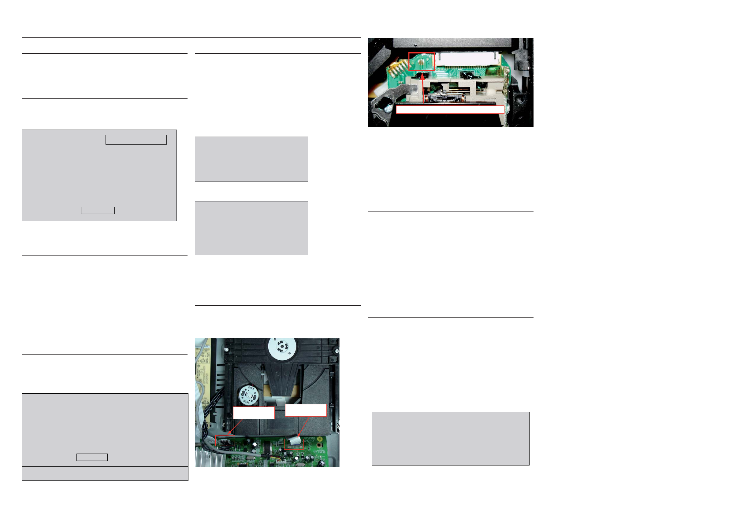
7) How to replace the defective DVD Loader
a) Remove the defective DVD Loader (see chapter 3).
b) Accordingly connect DVD Loader and “CN201”, “CN203” on the
top of main board as shown below
The ESD protection point on the Top side view of OPU
Note: The ESD protection point on t
be soldered if
- the DVD Loader is OK and needs to be disconnected from
connector “CN201” and “CN203” of the main board.
- the defective DVD Loader is needed to be send back to supplier
for failure analysis and to support back charging evidence.
8) Produce to change Tuner grid (only for /98 version)
In some countries, you can switch the FM tuning grid between 50
kHz and 100 kHz. Changing the tuning grid erases all preset radio
stations.
a) Press<radio> button on R/C
b) Press <Stop> button on R/C.
c) Press and hold <Play> until (50 kHz) or (100 kHz) is displayed.
Note: repeaing the same action will toggle back to it previous
tunning grid setting.
The Top side view of OPU
he Top side view of OPU must
5) Check on software version
a) Press <SETUP> button on R/C.
b) Select <preference setup> ,then press <OK>.
c) Select <version info>,then press <OK>.
d) TV will show message as follow:
Current model: 2501-12/94
Version:00.07.02_0 Release:2010.06.10
Region:0 Servo:62.10.00.07
8032: 0F.01.00.09 Risc:01.00.00.04
MCU: 07.00 BootLoader: Er
OK
Press SETUP
to exit menu
CN203
CN201
CAUTION!
This information is confi dential and may not be
distributed.Only a qualifi
ed service person should
reprogram the Region Code.
Page 9

REPAIR INSTRUCTION
2 - 22 - 2
G
Power Supply
No working
G
Power Supply
No working
All Voltage
No Output
Check F901
Bad Causc Damage
Check BK3.3V
Working or Not
AC1 AC2 Voltage
No Output
+32.5V Voltage
No Output
-27V Voltage
No Output
+12V Voltage
No Output
+5.1V Voltage
No Output
BK3.3V Voltage
No Output
Check Requir IC901 IC904
And Its conn circuit
Check D905 Q901 IC901 ZD903
And Its Conjoint Part
Check D908 Q901 IC901
And Its Conjoint Part
Check D906 Q901 IC901
And Its Conjoint Part
Check D904 Q901 IC901
And Its Conjoint Part
Check D902 Q901 IC901
And Its Conjoint Part
Check D910 IC904 Q901 IC901
And Its Conjoint Part
Page 10

DISASSEMBLY INSTRUCTIONS
3 - 1 3 - 1
Dismantling of theTop & Front Panel Assemble
1) Open the DVD Tray by using the Open/Close Button while the Set is ON and disconnect the mains supply after removing the Tray
Cover.
Note: If this is not possible, the DVD Tray has to be open manually.
Take a mini screw driver about 2mm diameter and make a marking 24mm from the tip as shown in gure 2 . Place the set on its
side, insert the mini screw driver till the marking and slide it towards the left as shown in gure 1 until the Tray moves out of the Front
Panel.
2) Return the set to its upright position and remove the Tray Cover as shown in Figure 3 and close the tray manually by pushing it back
in.
Push
3) Loosen 6 screws and remove the Top Cover by lifting the rear portion upwards before sliding it out towards the rear.
- 4 screws “A” at the back panel as shown in gure 4.
- 1 screw “B” each on the left & right side as shown in gure 5.
A
Figure 4
B
Figure 5
mm2
24mm
Figure 1
Figure 2
Dismantling of the DVD Loader Module
1) Loosen 4 screws “ C “ at the DVD Loader Module as shown in gure 6.
C
Figure 3
Figure 6
Page 11

3 - 2 3 - 2
Dismantling of the VFD+USB Board
1) Loosen 7 screws “D” on the top of VFD+USB Board as shown in gure 7.
Figure 7
Dismantling of the POWER Board
1) Loosen 5 screws “G ” on the top of Power Board as shown in gure 10.
D
Dismantling of the MAIN Board
1) Loosen 4 screws “ E ” on the top of MAIN Board as shown in gure 8.
2) Loosen 5 screws “ F ” at the back panel as shown in gure 9.
E
Figure 8
G
Figure 10
SERVICE POSITIONS
Figure 9
F
Note:In some service positions the components or copper patterns of one board may risk touching its neighbouring pc boards or
metallic parts. To prevent such short-circuit use a piece of hard paper or other insulating material between them.
Page 12
4 - 1 4 - 1
SUBWOOFER
SUBWOOFER
FRONT
RIGHT
FRONT
RIGHT
FRONT
LEFT
FRONT
LEFT
FRONT
CENTER
FRONT
CENTER
REAR
RIGHT
REAR
RIGHT
REAR
LEFT
REAR
LEFT
REAR
LEFT
REAR
RIGHT
FRONT
LEFT
FRONT
CENTER
FRONT
RIGHT
SUBWOOFER
CIRCUIT DIAGRAM
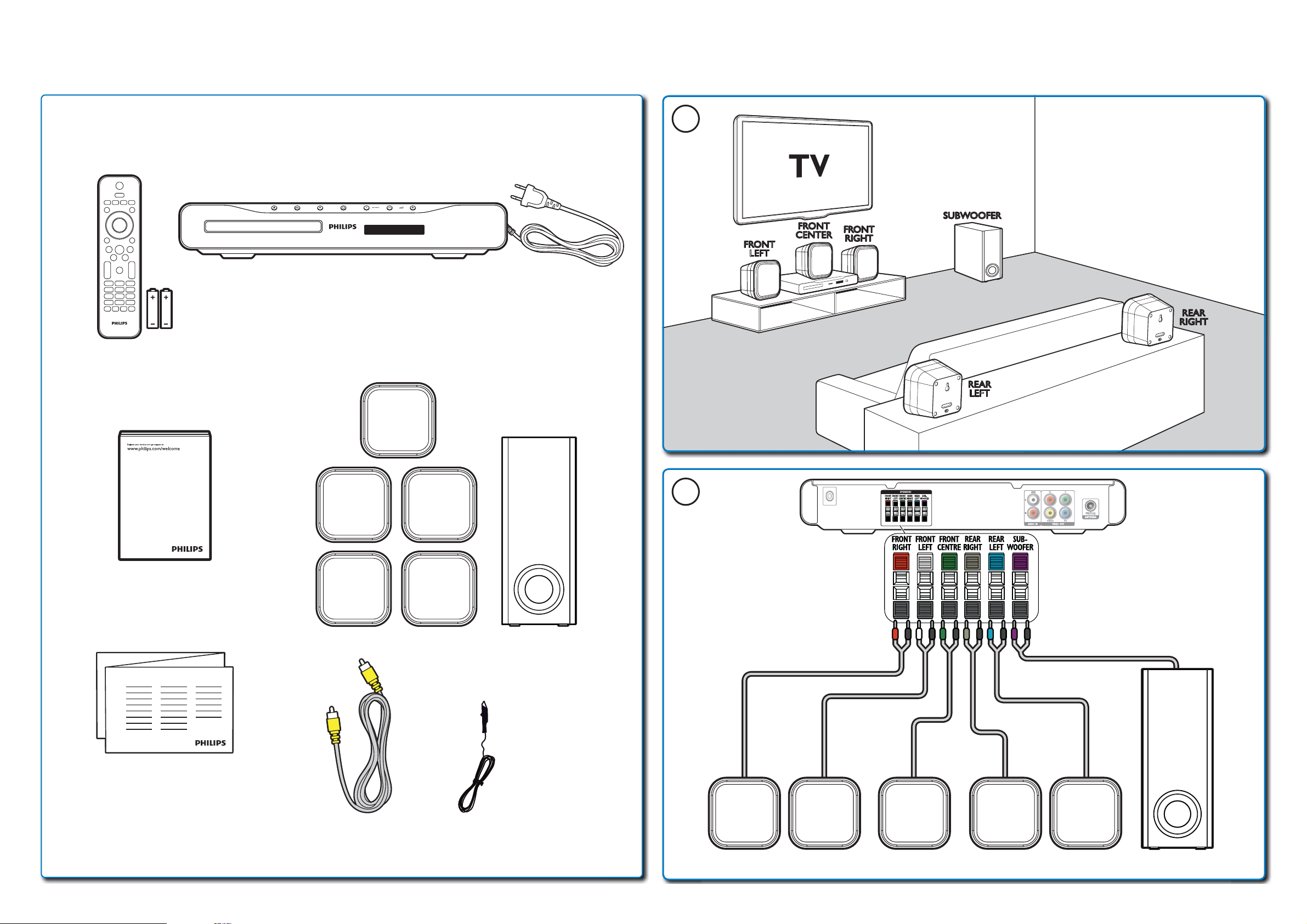
The following excerpt of the QSG/DFU serves as an introduction to the set.
The complete Direction for Use can be download in the different languages from the internet site of Philips Consumer care Center: www.support.philips.com
1
User Manual
2
Composite
FM Antenna
Page 13

4 - 2 4 - 2
3
4
Video
Cable
FM
Antenna
Audio
Cable
6
AAA
x 2
5
1
2
Page 14

4 - 3 4 - 3
USB
Settings
TV
AV
HOME THEATER
HOME THEATER
General Setup
OSD Language
Screen Saver
Screen Saver
OSD Language
Display Dim
Sleep Timer
DivX(R) VOD Code
Українська
General Setup
Русский
Display Dim
OSD Language
Screen Saver
Screen Saver
Sleep Timer
DivX(R) VOD Code
Melayu
ไทย
ύЎ!)䳾ᥟ*!
English
ύЎ!)ᕷᡏ*!
Auto
OSD Language
1
1
3
2
2
3
4
5
1
2
3
Page 15

4 - 4 4 - 4
User Manual
w
2
1
ww.philips.com/support
Specifications are subject to change without notice
Trademarks are the property of Koninklijke Philips Electronics N.V.
or their respective owners
2010 © Koninklijke Philips Electronics N.V. All rights reserved.
sgsna_1021/51,94,98_v1
Page 16

BLOCK DIAGRAM
5 - 1 5 - 1
Page 17

WIRING DIAGRAM
5 - 2 5 - 2
For tuner lead-in
CN201
For cvbs and rgb output
CN204
For AUX input
MAIN BOARD
CN202
CN203
CN302
CN902
For speaker output
For 220V input
V1V2
CN901
LOADER
CN903
V3
POWER BOARD
V5
USB BOARD
CN601
For usb input
CN601
VFD BOARD
Page 18

6 - 1 6 - 1
VFD+USB BOARD
FTD DISPLAY PIN ASSIGNMENT
TABLE OF CONTENTS
FTD Display Pin Assignment ............................................................. 6-1
Circuit Diagram ................................................................................. 6-2
PCB Layout Top & Bottom View ........................................................6-3
PIN CONNECTION
Page 19

CIRCUIT DIAGRAM
6 - 2 6 - 2
C601 B1
C602 B2
C603 D1
C604 B1
C605 B2
C606 B2
C607 B2
C608 B2
C609 C2
C610 A2
C611 B3
C612 C1
A
C613 C1
C614 C1
C615 C2
C616 B2
CN601 B1
CN602 D1
DP601 A2
IC601 C2
LD601 A1
Q601 A2
Q602 B1
R601 A1
R602 A1
R603 A1
R604 A1
R605 A1
R606 A1
R607 A2
R608 A2
R609 A2
R610 B3
R611 B1
R612 B1
R613 B1
R614 B2
R615 B2
R616 C1
R617 C1
R618 C1
R619 D1
R620 D1
R621 D1
R622 C1
R623 C1
R624 C1
R625 C1
SN601 A2
TA601 A1
TA602 A1
TA603 A1
TA604 A1
TA605 A2
TA606 A2
TA607 A2
USB601 D1
123
A
B
C
D
B
C
CN602
D
123
Page 20

PCB LAYOUT - TOP VIEW
6 - 3 6 - 3
C604 A2
C608 A4
C609 A2
CN601 A2
CN602 A1
DP601 A3
JM1 A3
JM10 A2
JM12 A2
JM3 A3
JM6 A3
JM7 A3
JM8 A3
JM9 A3
LD601 A2
SN601 A4
TA601 A4
TA602 A3
TA603 A3
TA604 A2
TA605 A2
TA606 A1
TA607 A1
USB601 A1
1234
A A
CN602
1234
PCB LAYOUT - BOTTOM VIEW
C601 A3
C602 A4
C603 A1
C605 A4
C606 A4
C607 A4
C610 A4
C611 A3
C612 A3
C613 A3
C614 A3
C615 A2
C616 A3
IC601 A3
Q601 A2
Q602 A2
R601 A3
R602 A3
R603 A3
R604 A3
R605 A2
R606 A2
R607 A1
R608 A1
R609 A4
R610 A3
R611 A2
R612 A2
R613 A3
R614 A4
R615 A4
R616 A3
R617 A3
R618 A3
R619 A3
R620 A3
R621 A3
R622 A3
R623 A3
R624 A3
R625 A3
1234
A A
1234
Page 21

7 - 1 7 - 1
A
d
INTERNAL IC DIAGRAM - MT1389DXE/J
MAIN+LED BOARD
TABLE OF CONTENTS
Internal IC Diagram ...........................................................................7-1
Circuit Diagram(part one) .................................................................. 7-2
Circuit Diagram(part two) ...................................................................7-3
Circuit Diagram(part three) ................................................................ 7-4
PCB Layout Top View .......................................................................7-5
PCB Layout Bottom View .................................................................. 7-6
DVD
PUH
Module
Motor
Drive
FLASH
ROM
DRAM
GPIO
IR/VFD
RF Amplifier
Servo IO
Spindle
Control
Memory
Controller
System
CPU
Debug
Servo
Processor
Audio
DSP
System
Parser
CPPM/CPRM
DRM
32-bit
RISC
Port
108MHz
TV Encoder
Video
Processor
Video Decoder
Audio
Ouptut
Video DAC
interlacer
MPEG-1/2/4
JPEG
6ch Audio DACs
USB 2.0 High
Speed
controller
MS/SD/MMC
Card
Controller
De-
Internal
PCM output
Internal
Audio ADC
CVBS, Y/C
Component
Video
6ch Audio Analog
outputs
Audio
DAC
SDPIF
USB 2.0 High
/ Full Speed
Device
MS/SD/MMC
Flash Card
Audio Mic1
Audio Mic2
INTERNAL IC DIAGRAM - TAS5508BPAG
AVDD_ PLL
AV SS_PLL
VDD_REF
VRD_ PLL
VR_P LL
MCLK
XTL_OUT
XTL_IN
PLL_FLTM
PLL_FLTP
OSC CAP
SCLK
LRCLK
SDIN1
SDIN2
SDIN3
SDIN4
SDA
SCL
RE SET
PDN
MUTE
HP_SEL
BKND_ERR
Clock, PLL, and Serial Date I/F
12C
Serial
Control
I/F
VRA_ PLL
VBGA P
Power Supply
D evice
Control
System Control
DA P Control
PWM Control
DVDD
AVDD
DV SS
AV SS
PWM_M PP and MR
PWM_M PP and ML
PWM AP and AM1 L Front
PWM AP and AM2 R Front
PWM AP and AM3 L Rear
PWM AP and AM4 R Rear
PWM AP and AM 7 Center
PWM AP and AM8
Subwoofer
PWM AP and AM 5 L Surround
PWM L Lineout
PWM AP and AM 5 R Surroun
PWM R Lineout
VALID
PS VS
8x8 Crossber Mixer
8
0
Det7Blquads
0
Det7Blquads
0
Det7Blquads
0
Det7Blquads
0
Det7Blquads
0
Det7Blquads
0
Det7Blquads
0
uads
Det7Blq
8 4
9
Soft
Tone
Soft
Tone
Soft
Tone
Soft
Tone
Soft
Tone
Soft
Tone
Soft
Tone
Soft
Tone
Volume
Control
Soft
Vol
Soft
Vol
Soft
Vol
Soft
Vol
Soft
Vol
Soft
Vol
Soft
Vol
Soft
Vol
Loud
Comp
Loud
Comp
Loud
Comp
Loud
Comp
Loud
Comp
Loud
Comp
Loud
Comp
Loud
Comp
8
DRC
DRC
DRC
DRC
DRC
DRC
DRC
DRC
PWM Section
DC
BlockDeEm ph
DC
BlockDeEm ph
DC
BlockDeEm ph
8x2 Crossber Mixer
2
2
DC
BlockDeEm ph
DC
BlockDeEm ph
DC
BlockDeEm ph
DC
BlockDeEm ph
DC
BlockDeEm ph
Interpolate SRC
Interpolate SRC
Interpolate SRC
Interpolate SRC
Interpolate SRC
Interpolate SRC
Interpolate SRC
Interpolate SR
NS PWM
NS PWM
NS PWM
NS PWM
NS PWM
NS PWM
NS PWM
NS PWM
C
Output Control
88
PS VC
Page 22

CIRCUIT DIAGRAM - part one
C401 D1
C402 A1
C403 A1
C404 A1
C405 A1
C406 A2
C407 A2
C408 B1
C409 B1
C410 B1
C411 B1
C412 B1
C413 B2
C414 B2
C415 A1
C416 A1
C417 A1
C418 B1
C419 A1
C420 B1
C421 A1
C424 B1
C425 B1
C426 B2
C427 B1
C428 B2
C429 B2
C430 B2
C431 B2
C432 B2
C433 B2
C434 B2
C436 C1
C437 D1
C438 C1
C439 A4
C440 C1
C441 C1
C442 C1
C443 C1
C444 C1
C445 C1
C446 C1
C447 C2
C448 C2
C449 C2
C450 A4
C451 A4
C452 D2
C454 C2
C455 D1
C456 D1
C457 C2
C458 A3
C459 A3
C460 B3
C461 B3
C462 A3
C463 B3
C464 C3
C465 D3
C466 C3
C467 D3
C468 D3
C469 D3
C470 A3
C471 A3
C472 B3
C473 C3
C474 C3
C475 D3
C476 A3
7 - 2 7 - 2
C477 A3
C478 B3
C479 B3
C480 B4
C481 B4
C482 B4
C483 B4
C484 C3
C485 C3
C486 D3
C487 D3
C488 D4
C489 D4
C490 D4
C491 D4
C492 A3
C493 A3
C494 B3
C495 B3
C496 B4
C497 B4
C498 C3
C499 C3
C500 D3
C501 D3
C502 D4
C503 D4
C504 A4
C505 A4
C506 A4
C507 B4
C508 B4
C509 B4
C510 B4
C511 B4
C512 B4
C513 C4
C514 C4
C515 C4
C516 D4
C517 D4
C518 D4
C519 D4
C520 D4
C521 D4
C522 A4
C523 C4
C524 A4
C525 B4
C526 B4
C527 C4
C528 D4
C529 D4
C532 C4
C533 C4
C534 A4
C535 A4
C536 A4
C537 C4
C538 C4
C541 C4
C542 A3
C543 D3
C544 B4
C545 B4
C546 B4
C547 B4
C548 D4
C549 D4
C550 D4
C551 D4
D401 C2
D402 C2
D403 C2
D404 C2
D407 C2
D408 D2
D409 D2
D411 D2
D412 C2
FB401 B1
FB402 B1
FB403 B1
FB404 B1
FB405 B1
FB406 B1
FB407 D1
IC401 A2
IC402 B2
IC403 A3
IC404 C3
JK401 C4
L401 A4
L402 A4
L403 B4
L404 B4
L406 C4
L407 D3
L408 D4
Q401 D1
Q402 B1
Q404 D2
R401 D1
R402 D1
R403 A1
R404 A1
R405 A1
R406 B2
R407 B2
R408 A1
R409 A1
R410 A1
R411 A1
R412 A2
R413 B2
R414 B2
R415 B2
R416 B2
R417 B2
R418 B2
R419 B2
R420 B2
R421 A1
R422 A1
R423 A1
R424 A2
R425 A3
R426 A2
R427 B3
R428 A2
R429 C3
R430 A2
R431 D3
R432 A2
R433 C2
R434 A2
R435 B2
R437 B1
R438 B1
R439 B1
R440 B2
R441 A2
R442 C1
R443 C1
R444 B2
R445 B2
R446 A4
R449 C1
R450 C1
R451 C2
R452 C1
R453 B1
R454 C2
R455 C2
R456 C2
R457 C1
1234
R458 C1
R459 C1
R460 C2
R462 C2
R463 C2
R464 C2
R465 C2
R466 C2
R467 C2
R468 C2
R470 D2
R471 D1
R472 A3
R473 A3
R474 B3
R475 B3
R476 C3
R477 C3
R478 D3
R479 D3
R480 A3
R481 C3
R484 A3
R485 C3
R486 A4
R487 B4
R488 B4
R489 C4
R490 D4
R491 D4
R492 A4
R494 B4
R495 B4
R496 C4
R498 D4
R499 D4
R500 A4
R501 A4
R502 B4
R503 B4
R504 B4
R505 B4
R506 C4
R507 C4
R508 D4
R509 D4
R510 D4
R511 D4
R512 B3
R513 D3
R514 B4
R515 B4
R516 B4
R517 B4
R518 D4
R519 D4
R520 D4
R521 D4
R522 C4
R523 C4
R525 D2
XL401 B1
ZD401 B1
ZD402 C2
A
B
C
A
B
C
D
D
1234
Page 23

CIRCUIT DIAGRAM - part two
C201 A2
C202 A2
C203 A2
C204 A2
C205 B2
C206 B2
C207 B2
C208 D3
C209 D3
C210 D3
C211 D4
C212 A2
C213 A2
C214 A2
C215 B2
C216 B2
C217 A3
C218 B4
C219 D4
C220 D4
C221 D4
C222 D4
C223 D4
C224 D4
C225 D4
C226 D3
C228 D3
C229 A1
C230 A1
C231 A1
C232 A1
C233 A1
C234 A1
C235 A1
C236 A1
C237 A1
C238 A1
C239 A1
C240 A1
C241 A1
C242 A1
C243 B1
C244 B1
C245 B2
C246 C1
C247 C1
C248 C1
C249 C1
7 - 3 7 - 3
C250 C1
C251 B1
C252 B1
C253 B1
C254 C1
C256 C1
C257 D1
C258 D1
C259 D1
C260 D1
C261 D1
C262 D1
C263 D1
C264 D1
C265 D1
C266 D1
C267 D2
C268 D2
C269 D2
C270 D3
C271 D3
C272 C3
C273 D2
C274 D2
C275 D1
C276 D2
C277 D2
C278 C2
C279 C3
C280 C2
C281 C2
C282 B1
C283 B1
C284 B1
C285 B1
C286 B1
C287 B2
C288 A4
C289 A4
C290 B4
C291 B4
C292 A4
C293 B4
CN201 B1
CN202 D1
CN203 D1
CN204 C2
CN205 B4
D209 C1
D211 B1
D212 B1
F201 C2
FB201 D3
FB202 A1
FB203 A1
FB204 A1
FB205 A1
FB206 D1
FB207 D1
FB209 D1
FB210 D1
FB211 D1
FB212 D1
FB213 D1
FB214 D1
FB215 D1
FB216 D1
FB217 D2
FB219 B1
IC201 B2
IC202 A4
IC203 D3
IC204 D4
IC205 D2
JK201 A2
L201 A2
L202 A2
L203 B2
L204 B2
L205 B2
L206 B4
L207 D3
L208 A1
L209 A1
L210 A1
L211 A1
L212 B1
L213 B1
L214 B1
L215 B1
L217 A4
L218 A4
Q201 B1
Q202 B1
Q208 B1
Q209 B1
R201 A2
R202 B2
R203 B3
R204 C2
R205 C2
R206 B2
R207 B2
R208 B2
R209 B3
R211 C3
R212 C3
R213 C3
R214 C3
R215 D3
R216 D3
R217 C3
1234
R218 C3
R219 D3
R220 D3
R221 A1
R222 A1
R223 A1
R224 A1
R225 A1
R226 A1
R227 D1
R228 B4
R229 B1
R230 B1
R231 B4
R232 C1
R233 C1
R237 C1
R238 C1
R239 C1
R240 C1
R242 D2
R243 D1
R244 D1
R246 D2
R247 D2
R250 D2
R251 D2
R252 C2
R253 C2
R256 B1
R257 B1
R258 B1
R259 B1
R260 B2
R261 B2
R262 A4
XL201 A2
ZD201 C3
ZD202 A1
ZD203 A1
A
B
A
B
C
D
C
D
1234
Page 24

CIRCUIT DIAGRAM - part three
C301 A1
C302 A2
C303 A2
C304 A2
C305 C2
C306 C2
C307 C2
C308 C2
C309 A2
C310 B3
C311 B3
C312 B3
C313 B4
C314 B4
C315 B4
C316 B4
C317 A1
C318 B3
C319 B4
C320 A1
C321 A1
C322 A1
C323 A1
C324 A2
C325 A2
C326 A2
C327 A2
C328 A3
C329 A3
C330 A3
C331 A3
C332 A4
C333 A4
C334 B1
C335 B1
C336 C1
C337 C1
C338 C1
C339 C1
C340 C1
C341 D1
C342 D1
C343 C2
C344 C2
C345 B3
C346 B3
C347 B4
C348 B4
7 - 4 7 - 4
C349 B3
C350 B3
C351 B3
C352 A1
C353 B3
C354 B3
C355 D3
C356 D3
C357 D3
C358 D3
C359 D3
C360 D3
C361 C3
C362 C3
C363 C3
C364 C3
C365 D3
C366 A1
C367 A1
C368 C4
C369 D3
C372 B3
C373 A1
CN302 B2
CN303 D4
FB301 A4
FB302 B1
FB303 B1
FB304 C2
FB305 D2
FB306 C2
FB307 C2
FB308 D2
FB309 C2
FB310 C2
FB311 C2
FB312 C2
FB313 C2
FB314 C2
IC301 A2
IC302 A3
IC303 B4
IC304 B4
IC305 D4
JK301 B1
L301 A1
L302 D3
L303 D3
Q301 B3
Q302 C3
Q303 C4
Q304 C4
Q305 C4
Q306 D4
Q307 D4
R302 A1
R303 A3
R304 A3
R305 A1
R306 A1
R307 A1
R308 A1
R309 A1
R310 A1
R311 A1
R312 A1
R313 A1
R314 A1
R315 A2
R316 A2
R317 A2
R318 A2
R319 A2
R320 A2
R321 A3
R322 A3
R323 A3
R324 A3
R325 A3
R326 A3
R327 A3
R328 A3
R329 A4
R330 A4
R331 C4
R332 A4
R333 A4
R336 B1
R337 B1
R338 B1
R339 B1
R340 B4
R345 B3
R346 B3
R347 C3
R348 C3
R350 C3
R351 C3
R352 D4
R353 D4
R354 D4
R355 D4
R356 D2
R357 C3
R358 C3
R359 C3
R360 C4
R361 D4
R362 D4
R363 D4
R364 D4
R365 D4
R366 D4
R367 D4
R368 D4
R369 D3
R370 D4
R371 D4
R372 D4
R373 C4
R374 C4
R375 C4
R376 C4
R377 D1
R378 D1
R379 D1
R383 D1
R384 D1
R385 D1
R386 D2
R387 D2
R388 D2
R389 C4
R390 C4
R391 C4
R392 C4
1234
R393 C4
R394 D3
R395 D3
R396 C2
R397 D4
R398 C2
R399 C2
TU301 D2
XL301 C3
ZD301 B3
ZD302 B3
ZD305 C3
A
B
A
B
C
D
C
D
1234
Page 25

PCB LAYOUT - TOP VIEW
C201 B1
C202 B1
C217 B1
C218 B2
C219 A2
C220 B2
C221 B2
C222 B2
C223 A2
C225 B2
C226 B2
C229 A1
C230 A1
C231 A2
C232 A1
C233 A1
C234 A1
C235 A1
C236 A2
C237 A1
C238 A1
C239 A1
C240 A2
C247 C2
C249 C2
C250 C2
C251 B1
C252 B1
C253 B1
C254 C1
C256 C1
C266 C2
C269 C2
C272 C3
C273 C2
C274 C2
C275 C2
C276 C2
C277 C2
C278 C2
C280 C2
C281 C2
C283 C3
C284 C4
C285 C3
C286 C2
C287 C3
C292 B1
C293 B1
C302 A1
C306 C5
C309 B1
C314 A3
C315 A2
C316 A2
C317 B1
C318 A2
C319 A2
C320 B1
C321 B1
C322 A1
C323 B1
C324 A1
C325 A1
C326 A1
C327 A1
C328 A2
C329 A2
C343 C5
C345 A2
C346 A2
C347 A3
C348 A2
C349 C5
C351 C5
C352 B1
C353 C5
C354 C5
C355 C3
C357 C3
C360 B3
C361 B3
C362 C2
C363 C3
C364 B2
C366 B1
C367 C1
C368 C3
C369 C3
C402 A3
C403 A3
C404 A3
C405 A3
C412 A3
C414 B3
12345
C415 A3
C416 A3
C417 A3
C418 A3
C419 A3
C420 A3
C424 B3
C425 B3
C426 A3
C427 A3
C436 A5
C437 C4
C440 C5
C441 C4
C442 B4
C443 B4
C444 B4
C445 A4
C446 A5
7 - 5 7 - 5
C447 A3
C448 A4
C452 A3
C455 B3
C456 C4
C457 A4
C458 A3
C459 A4
C460 B3
C461 A3
C462 A3
C463 B4
C464 B3
C465 B3
C466 B4
C467 B3
C468 B3
C469 C4
C470 A4
C471 A4
C472 B4
C473 B4
C475 C4
C476 A4
C477 A4
C478 A4
C479 A4
C484 B4
C485 B4
C486 B4
C487 B4
C492 A4
C493 A4
C494 A4
C495 B4
C498 B4
C499 B4
C500 B4
C501 C4
C504 A4
C507 B4
C508 A4
C513 B4
C516 B4
C517 C4
C522 A4
C523 B4
C524 A4
C525 A5
C526 A5
C527 A5
C528 A5
C529 A5
C532 B4
C533 B5
C542 A4
C543 B4
C544 B4
C545 A4
C546 B5
C547 B5
C548 C5
C549 C4
C550 C4
C551 C5
CN201 C1
CN202 C3
CN203 C3
CN204 C2
CN205 B2
CN302 C4
CN303 B2
D209 C2
D211 C3
D212 C3
D408 A3
F201 C2
FB201 A2
FB202 A1
FB203 A2
FB204 A1
FB205 A1
FB206 C2
FB207 C2
FB210 C2
FB211 C2
FB212 C2
FB213 C2
FB215 C2
FB216 C2
FB217 C3
FB219 C3
FB301 A2
FB302 A2
FB303 A2
FB304 C3
FB305 C3
FB306 C3
FB307 C3
FB308 C3
FB309 C4
FB310 C4
FB311 C4
FB312 C4
FB313 C5
FB314 C4
FB401 C5
FB402 C5
FB403 B5
FB404 B4
FB405 B5
FB406 B4
FB407 C4
IC201 B2
IC202 B1
IC203 B2
IC204 B2
IC205 C2
IC301 B1
IC302 A3
IC303 A2
IC304 B2
IC305 B3
IC401 A3
IC403 A4
IC404 B4
JK201 A1
JK301 A2
JK401 A5
L208 A1
L209 A1
L210 A1
L211 A2
L212 C2
L213 B1
L214 C1
L215 C1
L301 C1
L302 C3
L303 B3
L401 A5
L402 A4
L403 B5
L404 B5
L406 B5
L407 B5
L408 B5
Q201 C1
Q202 B1
Q208 C3
Q209 C3
Q301 C5
Q302 B2
Q303 C3
Q304 C3
Q305 C3
Q307 B3
Q402 B3
Q404 A3
R201 B1
R202 B2
R203 B2
R204 B2
R205 B2
R206 C2
R207 B2
R208 B2
R209 B2
R212 A2
R213 A2
R214 A2
R215 A2
R216 A2
R218 A2
R220 A2
R221 A1
R222 A1
R223 A1
R224 A2
R225 A1
R226 A1
R227 C2
R228 B2
R229 B1
R230 B1
R231 B2
R232 C2
R233 C2
R237 C2
R238 C2
R239 B2
R240 B1
R242 C2
R243 C2
R244 C2
R247 C2
R250 C2
R251 C2
R252 B2
R253 C2
R256 C3
R258 C3
R259 C3
R262 B1
R303 A3
R304 A3
R305 B1
R306 B1
R307 A1
R308 B1
R309 A1
R310 B1
R31
1 B1
R312 A1
R313 A1
R314 B1
R315 A1
R316 A1
R317 A1
R318 B1
R319 A1
R320 B1
R327 A3
R328 A3
R329 A2
R330 A2
R331 B3
R332 A3
R333 A2
R336 A2
R337 A2
R338 A2
R339 A3
R340 A2
R345 C5
R346 C5
R347 B2
R348 B2
R350 C3
R351 B2
R352 B3
R353 B3
R354 B3
R357 B3
R358 B3
R359 B3
R360 B3
R361 B2
R362 B2
R363 B3
R364 B3
R365 B3
R366 B3
R367 B3
R368 B2
R369 C3
R370 B2
R371 B3
R372 B3
R373 B3
R374 C3
R375 C3
R376 C3
R379 B3
R383 C3
R389 B3
R390 B3
R391 B3
R392 B2
R393 B2
R394 B3
R395 B3
R397 B2
R403 A3
R404 A3
R405 A3
R408 A3
R409 A3
R410 A3
R411 A3
R412 B3
R413 A3
R414 A3
R415 A3
R416 A3
R417 A3
R418 A3
R419 A3
R420 A3
R421 B3
R422 A3
R423 A3
R424 A3
R425 A3
R426 B3
R427 A3
R428 B3
R429 B3
R430 B3
R431 B3
R432 B3
R434 B3
R438 A3
R439 A3
R440 B3
R441 A3
R443 A5
R445 A3
R453 A5
R455 A3
R470 A3
R472 A3
R473 A4
R474 B3
R475 B4
R476 B3
R477 B4
R478 C3
R479 C4
R480 A3
R481 B3
R484 A3
R485 B3
R486 A4
R487 A4
R488 B4
R489 B4
R490 B4
R491 C4
R512 A3
R513 B3
R515 B5
R519 B5
R520 B5
R525 A3
TU301 B1
XL201 B1
XL301 C3
XL401 A3
ZD201 C2
ZD202 A1
ZD203 A1
ZD305 C5
ZD402 A3
A
B
C
A
B
C
12345
Page 26

PCB LAYOUT - BOTTOM VIEW
C203 B1
C204 B1
C205 B2
C206 B2
C207 B2
C208 B2
C209 B2
C210 B2
C211 B2
C212 B1
C213 B1
C214 B2
C215 B2
C216 B2
C224 B2
C228 A2
C241 A1
C242 A2
C243 C2
C244 B1
C245 B1
C246 C1
C248 C1
C257 C3
C258 C4
C259 C3
C260 C3
C261 C4
C262 C4
C263 C3
C264 C3
C265 C3
C267 C2
C268 C2
C270 C2
C271 C3
C279 C2
C282 C4
C288 B1
C289 B1
C290 B1
C291 B1
C301 B1
C303 B3
C304 B3
C305 C4
C307 C4
C308 C4
C310 A2
C311 A2
C312 A2
C313 A3
C330 A2
C331 A2
C332 A2
C333 A2
C334 A2
C335 A2
C336 C4
C337 C4
7 - 6 7 - 6
C338 C4
C339 C4
C340 C4
C341 C4
C342 C4
C344 C4
C350 C5
C356 B3
C358 B3
C359 B3
C365 B3
C372 A3
C373 A1
C401 A3
C406 A3
C407 B3
C408 B3
C409 A3
C410 A3
C411 A3
C413 B3
C421 A3
C428 A3
C429 A3
C430 A3
C431 A3
C432 A3
C433 A3
C434 A3
C438 C5
C439 A4
C449 A5
C450 A4
C451 A4
C454 A5
C474 B4
C480 A5
C481 A5
C482 B5
C483 B5
C488 B5
C489 B5
C490 B5
C491 B5
C496 A5
C497 B5
C502 B5
C503 A5
C505 A4
C506 A4
C509 B5
C510 A5
C511 A5
C512 B5
C514 B5
C515 B5
C518 A5
C519 A5
C520 B5
C521 C5
C534 A4
C535 A4
C536 A5
C537 B5
C538 B5
C541 A5
D401 A5
D402 A5
D403 A5
D404 A5
D407 A5
D409 A3
D411 A3
D412 A5
FB209 C3
FB214 C4
IC402 A5
L201 B1
L202 B1
L203 B1
L204 B2
L205 B2
L206 B2
L207 B2
L217 B1
L218 B1
Q306 B3
Q401 A3
R211 A2
R217 A2
R219 A2
R246 B2
R257 C3
R260 C3
R261 C3
R302 B1
R321 A2
R322 A2
R323 A3
R324 A3
R325 A3
R326 A3
R355 B3
R356 A1
R377 B3
R378 B3
R384 B3
R385 B3
R386 B3
R387 B3
R388 B3
R396 C5
R398 C5
R399 C5
R401 A3
R402 A3
R406 A3
R407 A3
R433 A4
R435 A2
R437 B3
R442 A5
R444 A4
R446 A4
R449 A5
R450 A5
R451 A4
R452 A5
R454 A2
R456 A5
R457 A5
R458 A5
R459 A5
R460 A5
R462 A4
R463 A4
R464 A5
R465 A5
R466 A5
R467 A5
R468 A5
R471 B3
R492 A4
R494 A5
R495 B5
R496 A5
R498 B5
R499 A5
R500 A4
R501 A4
R502 B5
R503 A5
R504 A5
R505 B5
R506 B5
R507 B5
R508 A5
R509 A5
R510 B5
R511 C5
R514 B4
R516 B4
R517 B4
R518 B4
R521 C5
R522 B4
R523 B5
ZD301 A2
ZD302 A2
ZD401 B3
12345
A
B
C
A
B
C
12345
Page 27

8 - 1 8 - 1
+
-
POWER BOARD
INTERNAL IC DIAGRAM - AZ431
CATHODE
REF
REF
V
TABLE OF CONTENTS
Internal IC Diagram ...........................................................................8-1
Circuit Diagram .................................................................................. 8-2
PCB Layout Top View .......................................................................8-3
PCB Layout Bottom View .................................................................. 8-4
ANODE
Page 28

CIRCUIT DIAGRAM
BD901 A1
C902 B1
C903 C1
C904 B1
C905 B1
C906 B1
C907 A1
C910 A1
C912 A1
C913 C2
C914 C2
C915 C2
C916 C2
C917 B1
C922 A3
C925 A3
C926 A4
C929 A3
C930 B2
C932 A3
C933 A3
C934 C3
C935 C3
C936 C3
8 - 2 8 - 2
C938 B4
C939 A3
C940 B4
C941 B4
C942 A3
C943 B2
C944 A3
C945 A3
C946 A3
C947 B4
C948 B4
C949 A3
C950 A3
C951 A3
C952 A4
C953 A3
C954 A3
C956 A3
C961 C3
C962 A1
C963 C4
C964 A1
C966 A1
C967 A1
C968 A4
CN901 C1
CN902 B4
CN903 A4
D901 A1
D902 A3
D903 B2
D904 A3
D905 A2
D906 A3
D907 A2
D908 A3
D909 B2
D910 B2
D911 C2
D912 C3
F901 C1
GT902 B1
IC901 B1
IC902 C2
IC903 C3
IC903 C3
IC904 B4
L901 B1
L902 A3
L903 A3
L904 A3
L905 A3
NTC901 C1
Q901 A2
Q903 B2
Q904 B2
Q905 A3
Q906 C3
Q907 C3
R901 C1
R902 C1
R903 C1
R904 B1
R905 B1
R906 B1
R908 A1
R911 B1
R912 B2
R913 B2
R914 B2
R915 C2
R916 C2
R917 B2
R918 B2
R919 B2
R920 B2
R921 A1
R922 B2
R923 A3
R924 A3
R925 A3
R926 A3
R927 B2
R928 A3
R929 A2
R930 A2
R932 C3
R933 A4
R934 B2
R935 C3
R936 A3
R937 A3
R938 C3
R939 C3
R940 A3
R941 C3
R942 A3
R943 C4
R944 C4
R945 A4
R946 A4
R947 A4
R960 B1
R961 C1
R962 B2
R963 B2
R964 C4
T901 A2
T901 A2
TVR901 C1
ZD901 C1
ZD901 C1
ZD902 B2
ZD903 A4
ZD904 A2
1234
A
B
A
B
C
C
1234
Page 29

PCB LAYOUT - TOP VIEW
BD901 B1
C902 B1
C903 A3
C904 D1
C906 C1
C907 B1
C910 A2
C912 A1
C913 C3
C914 B3
C915 B2
C916 B3
C917 B3
C922 D2
C930 B4
C932 C4
C933 D4
C935 C4
C938 C4
C939 C4
C940 D4
C946 C3
C947 D3
C949 D2
8 - 3 8 - 3
C950 D3
C951 D2
C952 D3
C962 B1
C966 A2
C967 B2
CN901 D1
CN902 D4
CN903 A4
D902 C3
D903 B4
D904 C3
D905 C3
D906 C3
D907 A3
D908 D2
D909 B4
D910 C3
D912 C4
F901 D2
GT902 C2
IC903 B4
IC903 B4
J901 B1
J902 B2
J903 A3
J904 A3
J905 A4
J906 A4
J907 B3
J908 C4
J909 C4
J910 D4
J912 D4
J913 D4
J914 D4
J915 D3
J916 D3
J917 D3
L901 C2
L902 C3
L903 D3
L904 D2
L905 D3
NTC901 D1
Q901 A2
Q903 B4
Q904 A4
Q905 C4
R906 B1
R912 B4
R914 B4
R918 A2
R923 C3
R924 D4
R930 A2
T901 C2
T901 C2
TVR901 D1
1234
A
B
A
B
C
D
C
D
1234
Page 30

PCB LAYOUT - BOTTOM VIEW
C905 A3
C925 D3
C926 D4
C929 C2
C934 B4
C936 C4
C941 D4
C942 C3
C943 C3
C944 C3
C945 D3
C948 D3
C953 D3
C954 D3
C956 D3
C961 D4
C963 C4
C964 A3
C968 D4
D901 A3
D911 B4
IC901 B3
IC902 B4
IC904 C4
Q906 D4
8 - 4 8 - 4
Q907 C4
R901 B3
R902 C1
R903 C1
R904 C1
R905 C1
R908 B3
R911 B3
R913 B4
R915 C3
R916 B4
R917 A4
R919 C3
R920 A3
R921 A2
R922 A3
R925 D2
R926 D2
R927 A2
R928 C4
R929 B3
R932 C4
R933 D3
R934 C3
R935 B4
R936 C4
R937 C4
R938 C4
R939 C4
R940 D4
R941 C4
R942 C4
R943 C4
R944 C4
R945 D3
R946 D3
R947 D3
R960 C1
R961 C1
R962 A3
R963 C3
R964 D4
ZD901 B4
ZD901 B4
ZD902 A4
ZD903 A4
ZD904 A2
1234
A
B
A
B
C
D
C
D
1234
Page 31

Mechanical Exploded View
9 - 1 9 - 1
35
MF
VIDEO
Only for:/55
for:/94/55/98
Only for:/12
33
34
for:/94/55/98
4 HSP140054-1060 SCREW T3.0x1.06PxL6mm NICKEL 17 HST143084-1080 SCREW M3.0x0.5PxL8mm NICKEL
6 HST143084-1060 SCREW M3.0x0.5PxL6mm NICKEL 19 HST143084-3060 SCREW M3x0.5PxL6mm BLACK OXIDE
14 HSP140054-1100 SCREW T3.0x1.06PxL10mm NICKEL 21 HSP140054-1080 SCREW T3.0x1.06PxL8mm NICKEL
Page 32

REVISION LIST
Version 1.0
*Initial release
10 - 1
Page 33

/12 /94
01
1 996510037149 DVD DOOR ABS L435XW11.2XD8.5MM BPD100309-0002
01
2 996510037187 FRONT DIS PANEL ABS 94HB W360X $ BPF106071-0001
01
3 996510037492 FUNCTION BUTTION ASSY
WMA100019-0001
01
8 996510037179 VFD+USB PCB ASSY ABE108960-0001
01
9 996510037178 PVC SHEET L169XW138XT0.5MM BLK $ BFP121181-0001
01
10 996510037151 POWER PCB ASSY $ ABE109010-0001
--
01
10 996510037489 POWER PCB ASSY $ ABE109010-0002
--
01
11 996510031708 RUBBER FOOT BRF100095-0001
01
12 996510038371 PWR CORD 2P 1450MM BLACK VDE $ VPE003272-0130
--
01
12 YES 996510038372 PWR CORD 2P 1300MM BK INDIA $ VPE00320D-0020
--
01
15 996510041588 MAIN PCB ASSY ABE108950-0011
--
01
15 996510041464 MAIN PCB ASSY ABE108950-0008
--
01
16 996510041456 TOP COVER SECC W360XD285XT0.5 GSE100002-0003
01
18 YES 996510021248 DVD LOADER $ ABN110013-0003
01
18 YES 996510031719 DVD LOADER $ ABN110013-0006
01
22 996510021367 AC SOCKET 2P 2.5A 250V $ CJP011003-0030
--
01
23 996520032521 SHRINK TUBE DIA=5 L=20mm $ DTB005000-0200
--
01
24 996510031344 SHRINKAGE TUBE $ DTB120000-0301
--
01
V1 996510037166 FFC CABLE 30P 60MM UL20706 VFC300820-060R
01
V2 996510037159 C/W 5P 260MM 2468#26 RAINBOW VFL501244-220R
01
V3 996510037156 FFC CABLE 16P 100MM UL20706 VFC160820-1000
01
V4 996510036071 C/W 4P 120MM WHT-NC-NC-RED
VWA310012-0003
--
01
V5 996510037488 SHIELD WIRE 5P 430MM
VSW524445-043R
01
V6 996510032807 FFC CABLE 16P 300mm UL20798 P=1.0mm VFC160320-3000
Accessories Parts
01
FM 996510008251 FM ANT WIRE VTA400003-0060
01
FM 996510004177
TANTENNA 1500mm+2x850mmW/FEMALE PLUG
VTA200002-0020
--
01
RC 996510037162 REMOTE CONTROL 39 KEYS WIR139004-9504
01
VIDEO 996500013058 RCA CABLE 2P 1.2M VRC101008-0010
Speakers Assembly Parts
002 CSPK 996510037163 SPEAKER BOX-CENTER ANC5C2500-CK01 --
002 CSPK 996510041465 SPEAKER BOX-CENTER ANC502501-CK01 --
002 FLSPK 996510037161 SPEAKER BOX-M-LEFT
ANM5M2500-CK01
--
002 FLSPK 996510041454 SPEAKER BOX-M-LEFT
ANM502501-CK01
--
002 FRCRF 996510027049 RUBBER FOOT DUF003058-0002
002 FRSPK 996510037176 SPEAKER BOX-M-RIGHT
ANM5M2500-CK02
--
002 FRSPK 996510041457 SPEAKER BOX-M-RIGHT
ANM502501-CK02
--
002 RLSPK 996510037172 SPEAKER BOX-REAR-LEFT
ANU5U2500-CK01
--
002 RLSPK 996510041462 SPEAKER BOX-REAR-LEFT ANU502501-CK01 --
002
RRSPK 996510037152 SPEAKER BOX-REAR-RIGHT
ANU5U2500-CK02
--
002
RRSPK 996510041463 SPEAKER BOX-REAR-RIGHT ANU502501-CK02
--
002
SRF 996510010854 RUBBER FOOT -SUBWOOFER DUF503010-0012
002
SSPK 996510037155 SPEAKER BOX-SUBWOOFER
ANW5W2500-CK01
--
002
SSPK 996510041461 SPEAKER BOX-SUBWOOFER
ANW502501-CK01
--
Main Unit Parts
Description
Safety
PCM Code
HTS2501
Level
Item No.
Alternativ
e
12NC
Page 34

MAIN PCB ASSY
002 D209
YES
996510037153 PS DIODE BAT54C SOT-23 PHILIPS RCD100540-0130
002 D209
YES
996510041145 CHIP DIODE BAT54C SOT-23 CJ RCD100540-0110
002 D211 996510010358 DIODE 1N4007 RAD114007-1010
002 D212 996510010358 DIODE 1N4007 RAD114007-1010
002 D401 996510010354 DIODE 1N4148W 100V SOD-123 CJ RCD114148-0012
002 D402 996510010354 DIODE 1N4148W 100V SOD-123 CJ RCD114148-0012
002 D403
996510010354
DIODE 1N4148W 100V SOD-123 CJ RCD114148-0012
002 D404 996510010354 DIODE 1N4148W 100V SOD-123 CJ RCD114148-0012
002 D407 996510010354 DIODE 1N4148W 100V SOD-123 CJ RCD114148-0012
002 D408 996510010354 DIODE 1N4148W 100V SOD-123 CJ RCD114148-0012
002 D409 996510010354 DIODE 1N4148W 100V SOD-123 CJ RCD114148-0012
002 D411 996510010354 DIODE 1N4148W 100V SOD-123 CJ RCD114148-0012
002 D412 996510010354 DIODE 1N4148W 100V SOD-123 CJ RCD114148-0012
002 F201 996500041960 PTC THERMISTOR RCT218121-1560
002 FB217 996500012470 BEAD FERITE 100 OHM/ AT 100MHZ SFB001001-0030
002 FB219 996500012470 BEAD FERITE 100 OHM/ AT 100MHZ SFB001001-0030
002 FB401 996500012470 BEAD FERITE 100 OHM/ AT 100MHZ SFB001001-0030
002 FB402
996500012470
BEAD FERITE 100 OHM/ AT 100MHZ SFB001001-0030
002 FB403 996500012470 BEAD FERITE 100 OHM/ AT 100MHZ SFB001001-0030
002 FB404 996500012470 BEAD FERITE 100 OHM/ AT 100MHZ SFB001001-0030
002 FB405 996500012470 BEAD FERITE 100 OHM/ AT 100MHZ SFB001001-0030
002 FB406 996500012470 BEAD FERITE 100 OHM/ AT 100MHZ SFB001001-0030
002 FB408 996500012470 BEAD FERITE 100 OHM/ AT 100MHZ SFB001001-0030
002 IC201 996510041589 IC 8P EN25F16-100HIP SOP EON AIC025016-C412 --
002 IC201 996510041455 IC 8P EN25F16-100HIP SOP EON 16 MBIT AIC025016-C410 --
002 IC202 996510037177 IC 128P MT1389DXE/J LQFP RCI13890J-0002
002 IC203 996510009895 IC 54P A641604L-6T TSOP II RCI641604-0001
002 IC204
994000005209
IC 3P AZ809NSTR-E1 SOT23 RCI000809-0008
002 IC204 996500041284 IC 3P STM809SWX6F 3.0V RCI000809-0012
002 IC205 996510012506 IC 28P AM5888S L/F HSOP AMTEK RCI005888-0001
002 IC205 996510010380 IC 28P A5888S HSOP RCI005888-0003
002 IC301 996510034346 IC 8P JRC4558 SOP ART RCI004558-0004
002 IC302 996510004287 IC 16P 4052L-S16-R SOP 4CH SW RCI004052-0006
002 IC302 994000000841 IC 16PIN TC4052BFN RCI004052-1001
002 IC302 996510009894 IC 16P CD4052BM SOIC TI RCI004052-1002
002 IC303 996510021056 IC 20P WM8781GEDS SSOP WOLFSON RCI008781-0001
002 IC304 996510016619 IC 14 PIN SN74HC04DR TI RCI740004-1001
002 IC305 996510041581 IC 44P STM8S105S6T6CTR LQFP ST AIC810566-C410 --
002 IC305 996510041458 IC 44P STM8S105S6T6CTR LQFP ST 16MHZ AIC810566-C408 --
002 IC401 996510021092 IC 64P TAS5508APAG TQFP TI RCI005508-0001
002 IC402 996510034346 IC 8P JRC4558 SOP ART RCI004558-0004
002 IC403 996510025677 IC 44P TAS5342LADDV HTSSOP RCI005342-0003
002 IC404 996510025677 IC 44P TAS5342LADDV HTSSOP RCI005342-0003
002 JK201 996510012542 RCA JACK4PRED-GRN/YEL-BLUW/GND CJR004301-0060
002 JK301 996510004632 RCA JACK 2P WHT-RED STAND CJR002601-0010
002 JK401 996510037174 SPK JACK 12P R-W-G-G-B-P/BKX6 CJS012103-0010
002 L401 996510025463 INDUCTOR 22UH SIN003704-2200
002 L402 996510025463 INDUCTOR 22UH SIN003704-2200
002 L403 996510025463 INDUCTOR 22UH SIN003704-2200
002 L404 996510025463 INDUCTOR 22UH SIN003704-2200
Page 35

002 L406 996510025463 INDUCTOR 22UH SIN003704-2200
002 L407 996510025463 INDUCTOR 22UH SIN003704-2200
002 L408 996510025463 INDUCTOR 22UH SIN003704-2200
002 Q201 996500026927 XISTR PNP 2SB1132RT100 ROHM HFE: RCP201132-1003
002 Q202 996500026927 XISTR PNP 2SB1132RT100 ROHM HFE: RCP201132-1003
002 Q208 996510000593 XISTR PNP 8550SS-D TO-92 CJ RAP008550-0001
002 Q209 996510000593 XISTR PNP 8550SS-D TO-92 CJ RAP008550-0001
002 Q301 996510000625 XISTR PNP 8550SL hFE160-300 RCP008550-0001
002 Q302
994000000915
XISTR NPN 2SC1623 RCN201623-1001
002 Q303 996500041281 FET 2N7002 60V/115MA
RCM207002-1002
002 Q304 996500041281 FET 2N7002 60V/115MA
RCM207002-1002
002 Q305 996500041281 FET 2N7002 60V/115MA
RCM207002-1002
002 Q306
996510000578
XISTR NPN KTC3875-Y RCN003875-1101
002 Q307 994000000921 XISTR PNP 2SA812 HFE:200-400 RCP200733-1001
002 Q401
996510000580
XISTR NPN MMS8050L RCN008050-1001
002 Q402 996500028742 XISTR NPN 2SD882P PB<1000PPM RHN200882-1001
002 Q404 996510000625 XISTR PNP 8550SL hFE160-300 RCP008550-0001
002 TU301 996510037175 TUNER PACK KST-MW004FV1-S78E WTP000011-0009
002 XL201 996510015057 CHIP CRYSTAL 27MHZ 20PPM 20PF JCQ012010-2760
002 XL301 996510015058 CHIP CRYST 12MHZ 30PPM 20pF JCQ313000-1260
002 XL401 996510021233 X'TAL 13.5MHz 15ppm 20pF JQC028100-1361
002 ZD201 996510028097 TVSESLC5VT523-3U RCU050523-4001
002 ZD202 996510031123 TVS PESD3V3S2UT SOT23 PHILIPS RCU030302-4001
002 ZD203
996510031123
TVS PESD3V3S2UT SOT23 PHILIPS RCU030302-4001
002 ZD301 996500021177 CHIP ZENR5.1V5%0.5W(E1)SOD-123 RCZ005005-0030
002 ZD302 996500021177 CHIP ZENR5.1V5%0.5W(E1)SOD-123 RCZ005005-0030
002 ZD305
994000005204
DIODE ZENR 12.6-13.1V 0.5W RAZ005012-1020
002 ZD401 996510031125 ZENER 4.0~4.6V 0.5W SOD-123 RCZ005004-0060
002 ZD402 994000005478 DIODE ZENER 9.1V 5% 0.5W RCZ005009-Z021
VFD+USB PCB
002 DP601 996510012856 VFD 32P KLV000044-0030
002 IC601 996500041280 IC 52P ET16311 VFD DRIVER RCI016311-0001
002 IC601 996500029614 IC 52P PT6311(PTC) RCI006311-1001
002 LD601 996510020167 LED 3 DIA ULTRA RED TINT CLEAR KED200003-0180
002 Q601 994000000921 XISTR PNP 2SA812 HFE:200-400 RCP200733-1001
002 Q602 994000000915 XISTR NPN 2SC1623 RCN201623-1001
002 SN601 996510032507 IRT RECEIVER IRM-3638TF4 RHO363804-2003
002 TA601 996510037188 TACT SW 2P 12V 50MA D3.5XH4.3M
MSW006014-0010
002 TA602 996510037188 TACT SW 2P 12V 50MA D3.5XH4.3M
MSW006014-0010
002 TA603 996510037188 TACT SW 2P 12V 50MA D3.5XH4.3M
MSW006014-0010
002 TA604 996510037188 TACT SW 2P 12V 50MA D3.5XH4.3M
MSW006014-0010
002 TA605 996510037188 TACT SW 2P 12V 50MA D3.5XH4.3M
MSW006014-0010
002 TA606 996510037188 TACT SW 2P 12V 50MA D3.5XH4.3M
MSW006014-0010
002 TA607 996510037188 TACT SW 2P 12V 50MA D3.5XH4.3M
MSW006014-0010
002 USB601 996500041955 USB JACK 4P AC 750V 1A CJU040005-0003
POWER PCB ASSY
002 BD901 996510032523 BRIDGE KBL406 4A 600V UL $ RHD204060-0040
002 C902 994000005344 CAP. SAFET. 560PF 400V 10% $ PVY1704K0-5610
002 C903 996510022033 COND MYLAR 0.0056uF 100V 5%
PRM0373A0-5620
Page 36

002 C904 996510029694 COND SAFETY 0.22uF 275V $ PVX2024G0-2240
002 C906 994000005344 CAP. SAFET. 560PF 400V 10% $ PVY1704K0-5610
002 C907 996510029694 COND SAFETY 0.22uF 275V $ PVX2024G0-2240
002 C910 996510030865 COND METAL 0.0022UF 630V 10% PVN0994P0-2220
002 C912 996500018042 COND DISC 0.01UF 1KV 20% PRD2355Q0-1030
002 C914 996500008286 COND MYLAR 0.022UF 100V 5%
PRM0373A0-2230
002 C915 994000005344 CAP. SAFET. 560PF 400V 10% $ PVY1704K0-5610
002 C916 994000005344 CAP. SAFET. 560PF 400V 10% $ PVY1704K0-5610
002 C929 996510008284 CHIP CAP 1000pF 1000V 10% PZL4564Q0-1020
002 C930 996510037154 COND ELECT 2.2UF 160V 20% 105 PRE0995C0-2290
002 C932 996510012511 COND ELECT 2.2 uF 100V PRE0395A0-2290
002 C933 996500020275 COND DISC 0.1UF 100V PRD3396A0-1040
002 C935 996510004633 COND MYLAR 0.1 uF 100V 5%
PRM0373A0-1040
002 C942 996510012513 CHIP CAP 470pF 500V 10% PZL4564M0-4710
002 C943 996510012513 CHIP CAP 470pF 500V 10% PZL4564M0-4710
002 C953 996510012861 CHIP CAP 0.1uF 100V 10% PZL4564A0-1040
002 C954 996510012861 CHIP CAP 0.1uF 100V 10% PZL4564A0-1040
002 C956 996510012861 CHIP CAP 0.1uF 100V 10% PZL4564A0-1040
002 C962 996510037185 COND ELECT 180UF 400V 20% $ PJE4995K0-1810 --
002 C962 996510041072
CODN ELECT 180uF 450V 20%105' D30xL30
$ PJE4995L0-1810 --
002 C962 996510041071
CODN ELECT 180uF 450V 20%?105' D30xL30
$ PJE4995L0-1811 --
002 C964 996510032497 CAP 1000PF 1000V 10% PZL4564Q4-1030
002 C966 996500018042 COND DISC 0.01UF 1KV 20% PRD2355Q0-1030
002 C967 996500018042 COND DISC 0.01UF 1KV 20% PRD2355Q0-1030
002 CN901 996510018268 CONNECTOR 4P P=3.96mm180' NICK $ CCN396141-0104
002 D901 996510010354 DIODE 1N4148W 100V SOD-123 CJ RCD114148-0012
002 D902 996510037167 GS DIODE SB560 DO-201AD 5A 60V RAD100560-0030
002 D903 994000000938 DIODE PR1507 1.5A 1000V RAD101507-1010
002 D904 996500038438 DIODE POWER RECTIFIER RHD100503-0010
002 D905 996510012516 DIODEHER105 DO-411A400V50nSFMS RAD100105-0010
002 D906 996510012516 DIODEHER105 DO-411A400V50nSFMS RAD100105-0010
002 D907 996510021223 DIODE PR2007 2A 1000V DO-15CTC RAD102007-0010
002 D908 996510032852 GS(S) DIODE FMX-G22S TO-220F RHD100220-0010
002 D909 996510012516 DIODEHER105 DO-411A400V50nSFMS RAD100105-0010
002 D910 996510012516 DIODEHER105 DO-411A400V50nSFMS RAD100105-0010
002 D911 996510010354 DIODE 1N4148W 100V SOD-123 CJ RCD114148-0012
002 D912 996510004297 IN5819 1A 28V SCHOTTKY RAD115819-1010
002 F901 996500017388 FUSE 3.15A 250V SLOW $ KSA020315-0121
002 GT902 996500029309 ABSORBER BL YP-501M 500V 500A L $ RAU000501-1001
002 GT903 996500029310
SURGE ABSORBER BL YP-141N 140V 0.8pF
$ RAU000141-1001
002 IC901 996510032491 IC 8P SSC620S SOP TAPE REEL $ RCI006200-0004
002 IC902 996510031429 CHIP OPTICAL SENSOR4P SOP $ RCO000817-3001
002 IC903 996500029312 IC 3 PIN TL431 TO-92 CHANG JIAN RHI004310-1101
002 IC903 994000000952 IC 3P TL431 RHI004310-1001
002 IC904 996510032504 IC 5P AP2125K-33TRG1 3.3V RCI212533-0001
002 L901 996510013776 LINE FILTER ET-24 7mH D0.7x44Ts 2UEW JFT001011-0010
002 L901 996510021225 LINE FILTER ET-24 7mH 2UEW D0.7x44Ts JFT001011-0030
002 L902 996500016694 6UH 13.5TS 2UEW SIL106002-6090
002 L903 996500016694 6UH 13.5TS 2UEW SIL106002-6090
002 L904 996500015871 INDUCTOR 10 UH 10% SAN001600-1000
002 L905 996500027104 INDUCTOR 6UH /-15% D=1.0MM PB SIL166001-0010
Page 37

002 NTC901 994000005232 THERMISTOR NTC 5R 5A $ RNT005130-5092
002 Q901 996510021085 MOSFET STK1060F TO220F AUK600V $
RHM001060-1001
--
002 Q901 996510032517 MOSFET SMK1080CI TO-3P 800V $
RHM001080-1001
--
002 Q903 996510004298 XISTR NPN 2N5551B TO-92 RAN205551-1002
002 Q904 996510004298 XISTR NPN 2N5551B TO-92 RAN205551-1002
002 Q905 996510012475 XISTR PNP 2N5401B TO-92 J. RAP205401-1002
002 Q906 994000000915 XISTR NPN 2SC1623 RCN201623-1001
002 Q907 994000000915 XISTR NPN 2SC1623 RCN201623-1001
002 R912 996510037158 RES 20K OHM 2W 5% FKK MOF
QGO205000-2030
002 R914 996510037158 RES 20K OHM 2W 5% FKK MOF
QGO205000-2030
002 R918 996510021241 RESISTOR 0.22R 3W 5% QKO305000-2280
002 T901 996510037164 SW TRANS ER35 8+8P 100W $ TSB000004-0018
002 T901 996510037165 SW TRANS EER35/42 8+8P 100W $ TSB000004-0014
002 TVR901 996510011373 METAL OXIDE VARISTOR 50A560V $ RPT050001-0040
002 ZD901 996510031129 ZENER 11.4-12.7V 0.5W SOD-123 RCZ005012-0030
002 ZD901 996510019996 ZENER 11.4-12.6V 0.5W RCZ005012-0040
002 ZD902 996510020001 ZENER 24V 5% 0.5W RCZ005024-0010
002 ZD903 996500019397 CHIP ZENER 5.6V 5% 0.5W RCZ005006-0011
Note : Only the parts with Philips 12NCs are normal Service spare parts.
'V' means existing spare parts; "--" means non existing spare parts.
Revsion List:
1.0 ###### Initial Released HTS2501/12/94
 Loading...