


INTEGRATED CIRCUITS
DATA SH EET
For a complete data sheet, please also download:
•The IC04 LOCMOS HE4000B Logic
Family Specifications HEF, HEC
•The IC04 LOCMOS HE4000B Logic
Package Outlines/Information HEF, HEC
HEF4755V
LSI
Transceiver for serial data
communication
Product specification
File under Integrated Circuits, IC04
January 1995
Philips Semiconductors Product specification
Transceiver for serial data communication
DESCRIPTION
The HEF4755V transceiver is a circuit for serial data
communication. It provides maximum transmission
security and effectiveness. Therefore, in addition to the
normal precautions, it contains a programmable digital
bit-check, a programmable CRC (Cyclic Redundancy
Check; Hamming distance 4 or 6) and format protection.
The circuit has 8 possible operating modes:
• synchronous
– error checking only
– receiving
– transmitting
– receiving with data out and transmitting the same
message
• asynchronous
– error checking only
– receiving
– transmitting
– receiving with data out and transmitting of a
regenerated message.
SUPPLY VOLTAGE/CURRENT
V
DD
I
SS
FAMILY DATA, I
See Family Specification
HEF4755V
LSI
RATING RECOMMENDED OPERATING
−0,5 to +15 4,75 to 12,6 V
30 − mA
LIMITS category LSI
DD
FEATURES
• Transmission rate:
V
DD
10 V 3,2 Mbaud 125 kbaud
• Inputs: standard LOCMOS
• Outputs: TTL compatible (1 TTL load)
• Operating ambient temperature range: −40 to + 85 °C
• Transmit or receive a serial binary data stream
• Start bit generation and recognition
• Format protection and checking
• Redundancy byte generation and checking
• Digital bit check
• Error recognition and error distinguishing
• 8-bit parallel input/output transfer
SYNCHRONOUS ASYNCHRONOUS
5 V 0,8 Mbaud 31 kbaud
7 V 1,6 Mbaud 62 kbaud
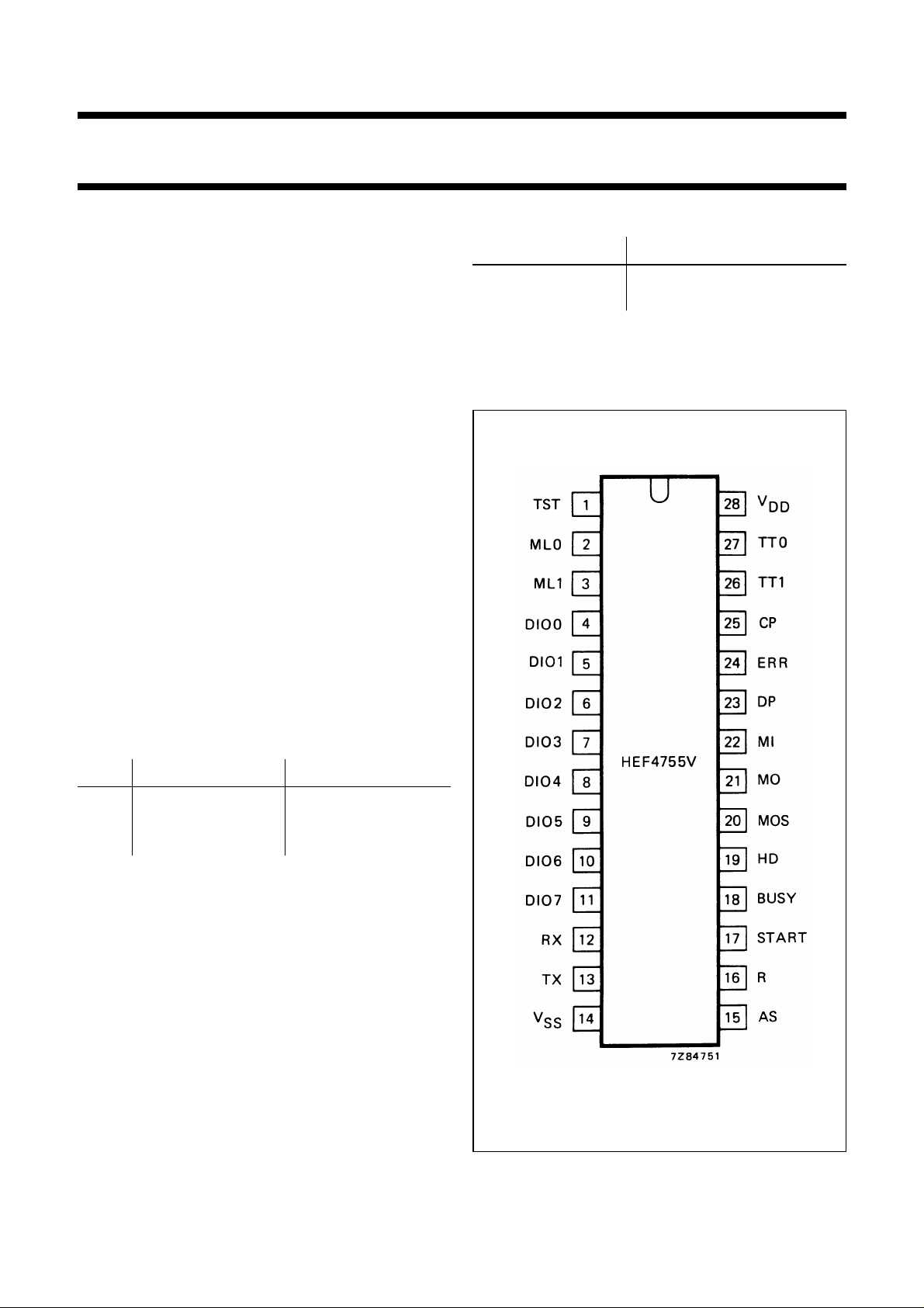
Fig.1 Pinning diagram.
January 1995 2

Philips Semiconductors Product specification
Transceiver for serial data communication
HEF4755VP(N): 28-lead DIL; plastic
(SOT117-2)
HEF4755VD(F): 28-lead DIL; ceramic (cerdip)
(SOT135)
HEF4755VT(D): 28-lead SO; plastic
(SOT136-1)
( ): Package Designator North America
PINNING
1 TST Test pin; during normal use
connected to V
HIGH (VDD), internal check points
are connected to the data bus.
2 ML0 Input code for message length (see
3 ML1
4 DIO0
11 DIO7
12 RX Mode input: receive; see Table 2
13 TX Mode input: transmit; see Table 2
15 AS Mode input: asynchronous;
16 R Reset; a positive signal resets
17 START Input start in transmitting mode;
18 BUSY Output busy; active during
Table 1).
Bidirectional data bus.to to
see Table 2
all internal registers.
synchronization input (from MOS)
in synchronous receiving mode.
receiving or transmitting a message.
. When TST is
SS
HEF4755V
LSI
19 HD Hamming distance; determines the
length of the redundancy byte:
LOW = 7 bit (HD = 4)
HIGH = 15 bit (HD = 6)
20 MOS Output message synchronization
used in synchronous mode.
21 MO Message output.
22 MI Message input.
23 DP Output data pulse; take-over pulse
for data on the data bus.
24 ERR Output error; an active output
means that at least 1 transmission
error is recognized.
25 CP Clock input; in synchronous mode
equal to the transmission bit rate.
26 TT1 Programming of the permissible time
27 TT0
28 V
14 V
DD
SS
tolerance in bit distortion
(see Table 3).
Positive supply voltage; 4,5 V to
12,5 V (is the logic HIGH level).
Ground (is the logic LOW level).
January 1995 3

Philips Semiconductors Product specification
Transceiver for serial data communication
Table 1 Input code for message length
ML0 ML1 MESSAGE LENGTH
H H 6 data bytes
L H 4 data bytes
H L 2 data bytes
variable length
LL
Table 2 Input code for input mode
RX TX AS
L L L status register connected to the data bus for error recognition
H L L receiving in synchronous mode
L H L transmitting in synchronous mode
H H L receiving messages (without redundancy bit); data parallel out;
L L H only bit check in asynchronous mode; no data output on data bus
H L H receiving in asynchronous mode
L H H transmitting in asynchronous mode
H H H receiving and transmitting of a regenerated message in the
depends on
format byte
calculating of redundancy byte; transmitting data with redundancy
byte in synchronous mode
asynchronous mode
HEF4755V
LSI
Table 3 Permissible time tolerance in bit distortion
TT1 TT0 PERMITTED DISTORTION (dt/T)
L L 6/32 ≈ 19%
L H 8/32 = 25%
H L 10/32 ≈ 31%
H H 12/32 ≈ 37%
Notes
1. H = HIGH state (the most positive voltage)
2. L = LOW state (the least positive voltage)
January 1995 4
 Loading...