

Philips HEF4750VU, HEF4750VDB, HEF4750VD, HEC4750VDB Datasheet

DATA SH EET
Product specification
File under Integrated Circuits, IC04
January 1995
INTEGRATED CIRCUITS
HEF4750V
LSI
Frequency synthesizer
For a complete data sheet, please also download:
•The IC04 LOCMOS HE4000B Logic
Family Specifications HEF, HEC
•The IC04 LOCMOS HE4000B Logic
Package Outlines/Information HEF, HEC

January 1995 2
Philips Semiconductors Product specification
Frequency synthesizer
HEF4750V
LSI
DESCRIPTION
The HEF4750V frequency synthesizer is one of a pair of
LOCMOS devices, primarily intended for use in
high-performance frequency synthesizers, e.g. in all
communication, instrumentation, television and broadcast
applications. A combination of analogue and digital
techniques results in an integrated circuit that enables high
performance. The complementary device is the universal
divider type HEF4751V.
Together with a standard prescaler, the two LOCMOS
integrated circuits offer low-cost single loop synthesizers
with full professional performance. Salient features offered
(in combination with HEF4751V) are:
• Wide choice of reference frequency using a single
crystal.
• High-performance phase comparator low phase
noise low spurii.
• System operation to > 1 GHz.
• Typical 15 MHz input at 10 V.
• Flexible programming:
frequency offsets
ROM compatible
fractional channel capability.
• Programme range 6
1
⁄2 decades, including up to
3 decades of prescaler control.
• Division range extension by cascading.
• Built-in phase modulator.
• Fast lock feature.
• Out-of-lock indication.
• Low power dissipation and high noise immunity.
APPLICATION INFORMATION
Some examples of applications for the HEF4750V in
combination with the HEF4751V are:
• VHF/UHF mobile radios.
• HF s.s.b. transceivers.
• Airborne and marine communications and navaids.
• Broadcast transmitters.
• High quality radio and television receivers.
• High performance citizens band equipment.
• Signal generators.
SUPPLY VOLTAGE
RATING RECOMMENDED OPERATING
−0,5 to +15 9,5 to 10,5 V
January 1995 3
Philips Semiconductors Product specification
Frequency synthesizer
HEF4750V
LSI
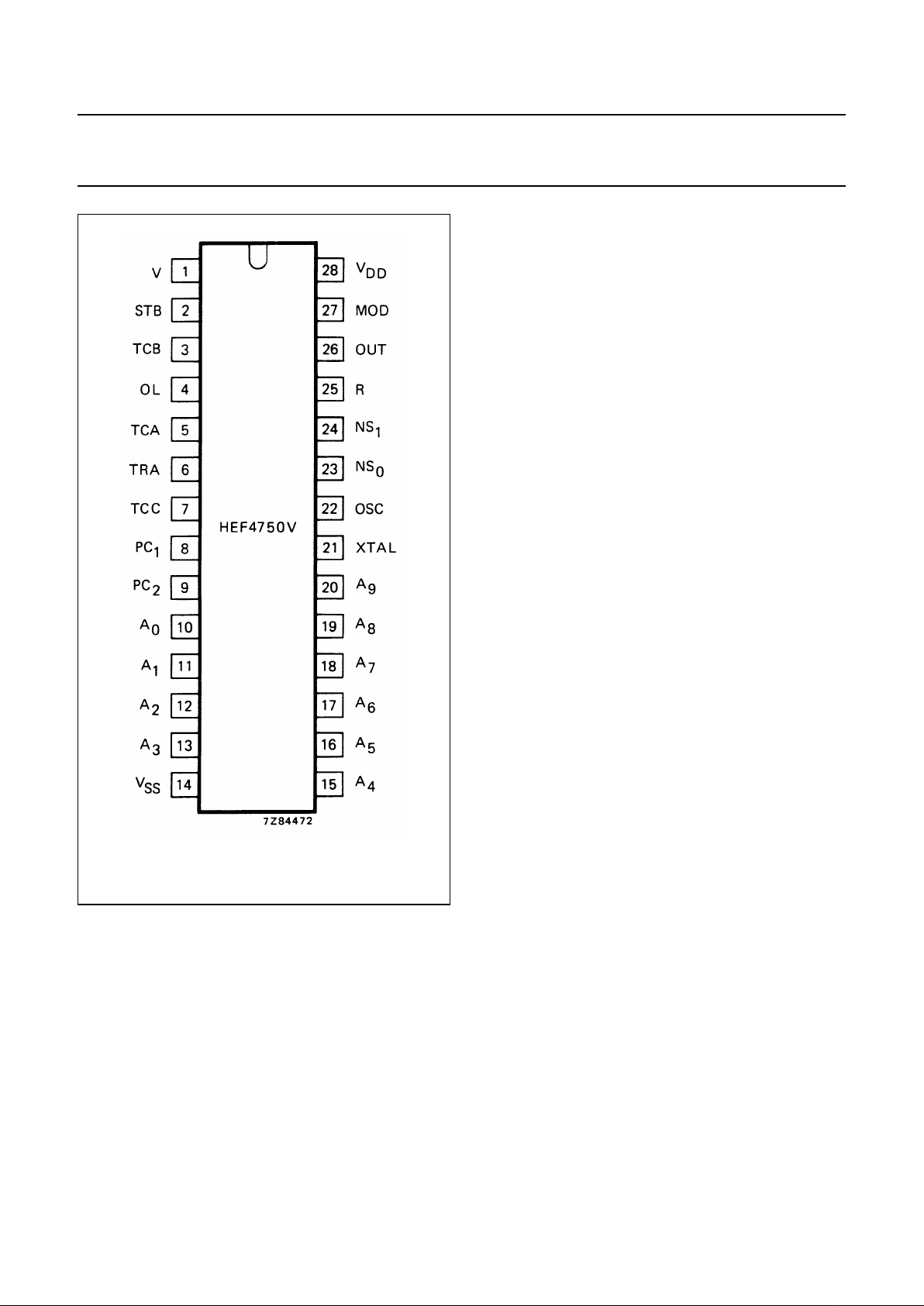
HEF4750VD(F): 28-lead DIL; ceramic (cerdip)
(SOT135)
( ): Package Designator North America
Fig.1 Pinning diagram.
PINNING
R phase comparator input, reference
V phase comparator input
STB strobe input
TCA timing capacitor C
A
pin
TCB timing capacitor C
B
pin
TCC timing capacitor C
C
pin
TRA biasing pin (resistor R
A
)
PC
1
analogue phase comparator output
PC
2
digital phase comparator output
MOD phase modulation input
OL out-of-lock indication
OSC reference oscillator/buffer input
XTAL reference oscillator/buffer output
A
0
to A
9
programming inputs/programmable divider
NS
0
, NS1programming inputs, prescaler
OUT reference divider output
January 1995 4
Philips Semiconductors Product specification
Frequency synthesizer
HEF4750V
LSI
This text is here in white to force landscape pages to be rotated correctly when browsing through the pdf in the Acrobat reader.This text is here in
_white to force landscape pages to be rotated correctly when browsing through the pdf in the Acrobat reader.This text is here inThis text is here in
white to force landscape pages to be rotated correctly when browsing through the pdf in the Acrobat reader. white to force landscape pages to be ...
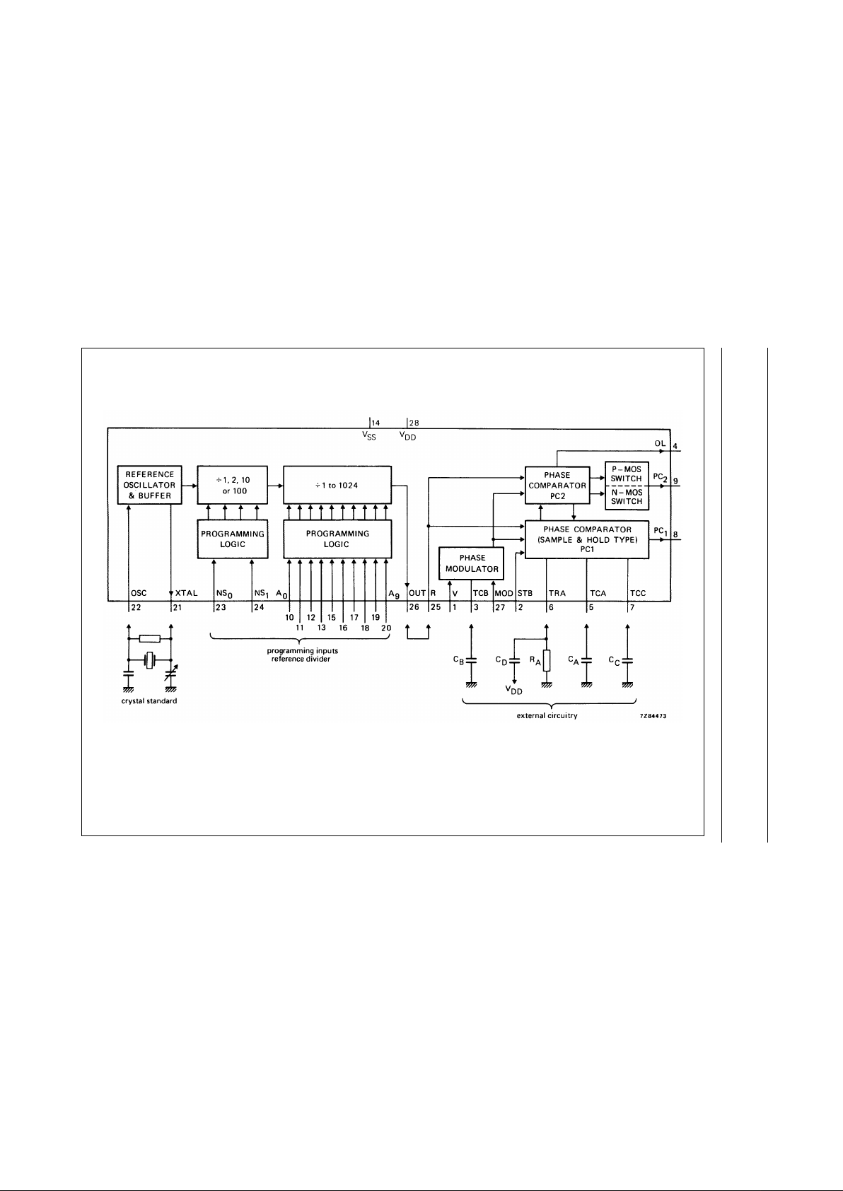
Fig.2 Block diagram comprising five basic functions: phase comparator 1 (PC1), phase comparator 2 (PC2), phase modulator, reference
oscillator and reference divider. These functions are described separately.
N.B. PC1= analogue output; PC2= 3-state output.
January 1995 5
Philips Semiconductors Product specification
Frequency synthesizer
HEF4750V
LSI
FUNCTIONAL DESCRIPTION
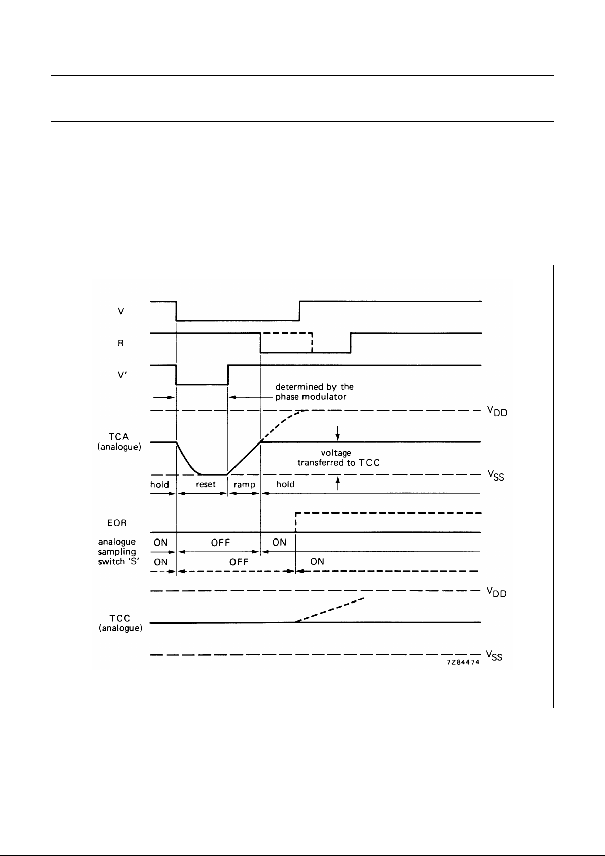
Phase comparator 1
Phase comparator 1 (PC1) is built around a SAMPLE and
HOLD circuit. A negative-going transition at the V-input
causes the hold capacitor (C
A
) to be discharged and after
a specified delay, caused by the Phase Modulator by
means of an internal V’ pulse, it produces a positive-going
ramp. A negative-going transition at the R-input terminates
the ramp. Capacitor C
A
holds the voltage that the ramp
has attained. Via an internal sampling switch this voltage
is transferred to CCand in turn buffered and made
available at output PC1.
If the ramp terminates before an R-input is present, an
internal end of ramp (EOR) signal is produced.
These actions are illustrated in Fig.3.
The resultant phase characteristic is shown in Fig.4.
Fig.3 Waveforms associated with PC1.
January 1995 6
Philips Semiconductors Product specification
Frequency synthesizer
HEF4750V
LSI
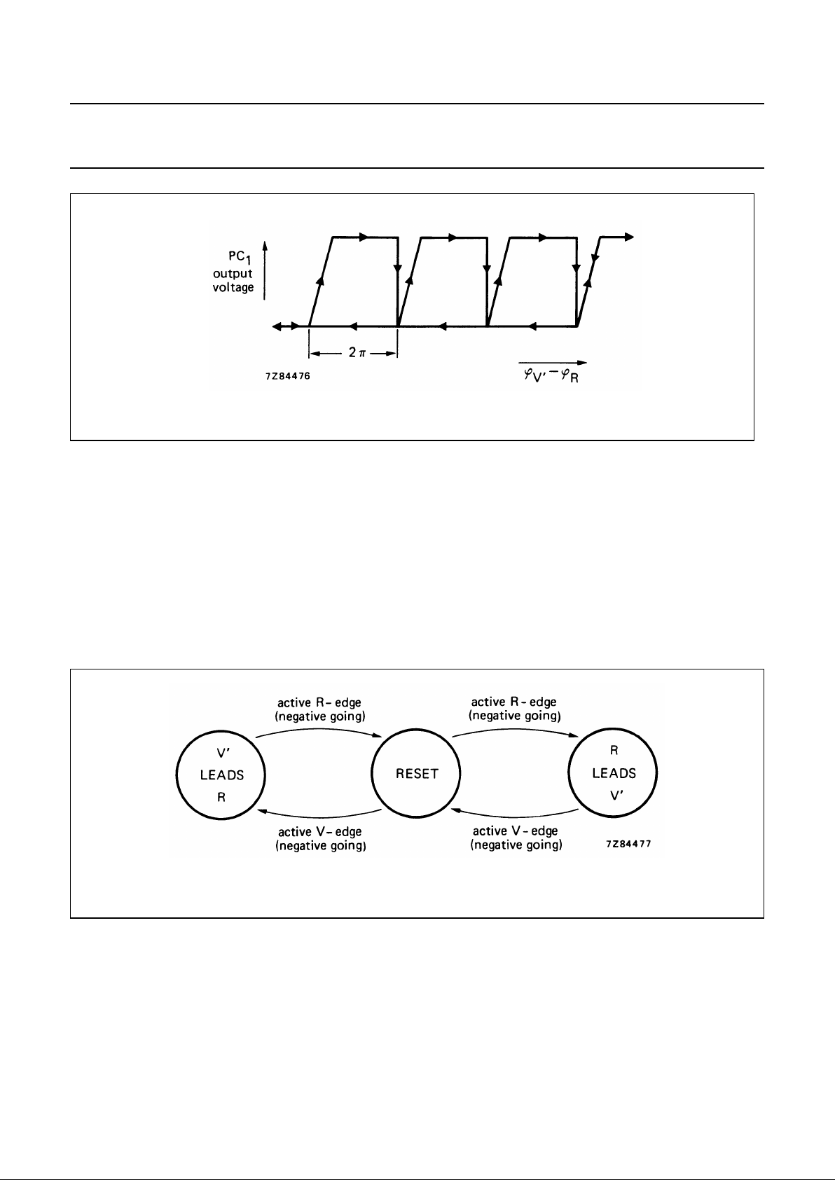
Fig.4 Phase characteristic of PC1.
PC1 is designed to have a high gain, typically 3200 V/cycle
(at 12,5 kHz). This enables a low noise performance.
Phase comparator 2
Phase comparator 2 (PC2) has a wide range, which
enables faster lock times to be achieved than otherwise
would be possible. It has a linear ± 360° phase range,
which corresponds to a gain of typically 5 V/cycle.
This digital phase comparator has three stable states:
• reset state,
• V’ leads R state,
• R leads V’ state.
Conversion from one state to another takes place
according to the state diagram of Fig.5.
Fig.5 State diagram of PC2.
Output PC2produces positive or negative-going pulses
with variable width; they depend on the phase relationship
of R and V’. The average output voltage is a linear function
of the phase difference. Output PC2remains in the high
impedance OFF-state in the region in which PC1 operates.
The resultant phase characteristic is shown in Fig.6.
 Loading...