

Philips HEF4720B, HEF4720V DATASHEETS

INTEGRATED CIRCUITS
DATA SH EET
For a complete data sheet, please also download:
•The IC04 LOCMOS HE4000B Logic
Family Specifications HEF, HEC
•The IC04 LOCMOS HE4000B Logic
Package Outlines/Information HEF, HEC
HEF4720B
HEF4720V
LSI
256-bit, 1-bit per word random
access memories
Product specification
File under Integrated Circuits, IC04
January 1995
Philips Semiconductors Product specification
HEF4720B
256-bit, 1-bit per word random access memories
HEF4720V
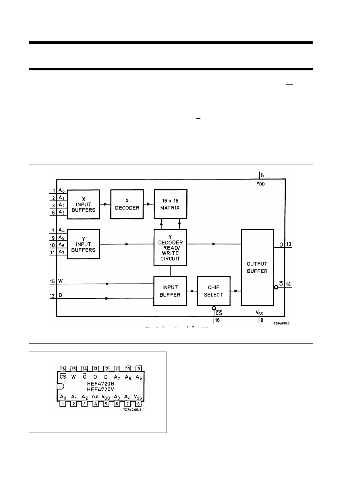
DESCRIPTION
The HEF4720B and HEF4720V are 256-bit, 1-bit per word
random access memories with 3-state outputs. The
memories are fully decoded and completely static.
Recommended supply voltage range for HEF4720B is 3 to
15 V and for HEF4720V is 4,5 to 12,5 V; minimum
stand-by voltage for both types is 3 V.
The use of LOCMOS gives the added advantage of very
low stand-by power. The circuits can be directly interfaced
with standard bipolar devices (TTL) without using special
interface circuits. The memory operates from a single
power supply. The separate chip select input (
simple memory expansion when the outputs are wire-O
Red. If CS is HIGH, the outputs are floating and no new
information can be written into the memory. The signal at
O has the same polarity as the data input D, while the
signal at O is the complement of the signal at O. The write
control W must be HIGH for writing into the memory.
CS) allows
Fig.1 Functional diagram.
Fig.2 Pinning diagram.
January 1995 2
HEF4720BP; HEF4720VP(N): 16-lead DIL; plastic
(SOT38-1)
HEF4720BD; HEF4720VD(F): 16-lead DIL; ceramic
(cerdip) (SOT74)
HEF4720BT; HEF4720VT(D): 16-lead SO; plastic
(SOT109-1)
( ): Package Designator North America
FAMILY DATA
See Family Specifications.
Philips Semiconductors Product specification
HEF4720B
256-bit, 1-bit per word random access memories
IDDLIMITS
See below.
HEF4720V
FUNCTION TABLE
CS W O O MODE
L H data written complement of data write
into memory written into memory
L L data written complement of data read
into memory written into memory
H X Z Z inhibit
PINNING
CS chip select input (active LOW)
W write enable input
D data input
A
0
to A
7
address inputs
O 3-state output (active HIGH)
O 3-state output (active LOW)
Notes
1. H = HIGH state (the more positive voltage)
L = LOW state (the less positive voltage)
X = state is immaterial
Z = high impedance OFF-state
SUPPLY VOLTAGE
RATING RECOMMENDED OPERATING STAND-BY MIN.
HEF4720B −0,5 to 18 3,0 to 15,0 3 V
HEF4720V −0,5 to 18 4,5 to 12,5 3 V
The values given at VDD= 15 V in the following DC and
AC characteristics, are not applicable to the HEF4720V,
because of its lower supply voltage range.
DC CHARACTERISTICS
=0 V
V
SS
T
(°C)
amb
V
V
DD
V
OL
V
SYMBOL
−40 +25 +85
MIN. MAX. MIN. MAX. MIN. MAX.
Output current 4,75 0,4 2,4 2 1,6 mA
LOW 10 0,5 I
OL
4,8 4 3,2 mA
15 1,5 10,0 10 7,5 mA
Quiescent device 5 25 25 200 µA
current 10 I
DD
50 50 400 µA
15 100 100 800 µA
Input leakage current
HEF4720V 10
HEF4720B 15 0,3 0,3 1 µA
±I
IN
0,3 0,3 1 µA
January 1995 3
Philips Semiconductors Product specification
HEF4720B
256-bit, 1-bit per word random access memories
AC CHARACTERISTICS
V
DD
SYMBOL MIN. TYP. MAX.
V
55pF
Output capacitance 10 C
15 5 pF
A.C. CHARACTERISTICS
V
SS
= 0 V; T
=25°C; CL= 50 pF; input transition times ≤ 20 ns
amb
O
5pF
HEF4720V
V
DD
V
SYMBOL MIN. TYP. MAX.
TYPICAL EXTRAPOLATION
FORMULA
Read cycle
5 320 580 ns 292 ns + (0,55 ns/pF) C
Read access time 10 t
ACC
130 220 ns 118 ns + (0,23 ns/pF) C
15 100 160 ns 92 ns + (0,16 ns/pF) C
Chip select to 5 180 ns
output time 10 t
CO
70 ns
15 50 ns
50ns
Address hold time 10 t
OA
0ns
15 0 ns
Output hold time 5 60 170 ns 142 ns + (0,55 ns/pF) C
with respect to 10 t
VAL1
20 50 ns 38 ns + (0,23 ns/pF) C
address input 15 15 40 ns 32 ns + (0,16 ns/pF) C
Output hold time 5 130 ns
with respect to 10 t
COH
70 ns
chip select input 15 60 ns
Output floating time 5 0 ns
with respect to 10 t
COF
0ns
chip select input 15 0 ns
5 580 ns
Read cycle time 10 t
RC
220 ns
15 160 ns
Output transition 5 60 120 ns 10 ns + (1,0 ns/pF) C
times 10 t
TLH
30 60 ns 9 ns + (0,42 ns/pF) C
LOW to HIGH 15 20 40 ns 6 ns + (0,28 ns/pF) C
54080ns14ns+(0,52 ns/pF) C
HIGH to LOW 10 t
THL
22 40 ns 11 ns + (0,22 ns/pF) C
15 15 30 ns 7 ns + (0,16 ns/pF) C
L
L
L
L
L
L
L
L
L
L
L
L
January 1995 4

Philips Semiconductors Product specification
HEF4720B
256-bit, 1-bit per word random access memories
AC CHARACTERISTICS
V
= 0 V; T
SS
Write cycle
Write cycle time 10 t
Address to write 5 110 ns
set-up time 10 t
Write pulse width 10 t
Write recovery time 10 t
Data set-up time 10 t
Data hold time 10 t
Chip select set-up 5 370 ns
time with respect 10 t
to write pulse 15 80 ns
Chip select hold 5 0 ns
time with respect 10 t
to write pulse 15 0 ns
Chip select lead time 5 0 ns
over write pulse to 10 t
prevent writing 15 0 ns
=25°C; CL= 50 pF; input transition times ≤ 20 ns
amb
V
DD
V
SYMBOL MIN. TYP. MAX.
5 580 ns
WC
220 ns
15 160 ns
AW
15 50 ns
5 370 10 000 ns
WP
130 10 000 ns
15 80 10 000 ns
5 100 ns
WR
15 30 ns
5 250 ns
DW
100 ns
15 80 ns
5 100 ns
DH
15 20 ns
CSW
CSH
CSL
130 ns
50 ns
40 ns
30 ns
0ns
0ns
HEF4720V
January 1995 5
 Loading...