Philips hef4527b DATASHEETS

INTEGRATED CIRCUITS
DATA SH EET
For a complete data sheet, please also download:
•The IC04 LOCMOS HE4000B Logic
Family Specifications HEF, HEC
•The IC04 LOCMOS HE4000B Logic
Package Outlines/Information HEF, HEC
HEF4527B
MSI
BCD rate multiplier
Product specification
File under Integrated Circuits, IC04
January 1995

Philips Semiconductors Product specification
BCD rate multiplier
DESCRIPTION
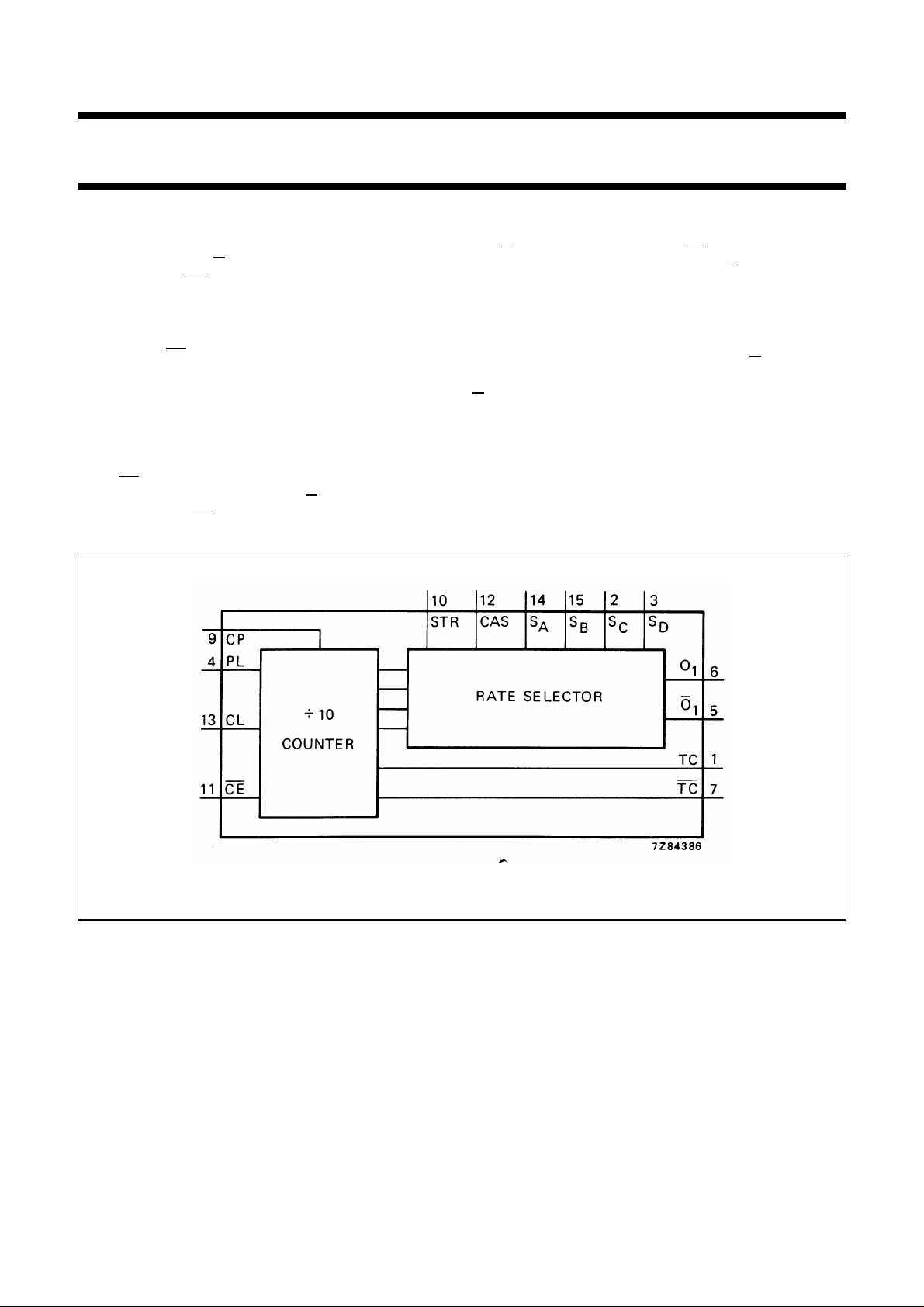
The HEF4527B is a BCD rate multiplier with two buffered
rate outputs (O1 and O1), two buffered terminal count
outputs (TC and TC), four BCD rate select inputs (SA, SB,
SC, SD), a common clock input (CP), a preset input (PL),
an overriding asynchronous clear input (CL), a strobe input
(STR), a cascade input (CAS) and an active LOW count
enable input (CE).
The BCD rate multiplier provides an output pulse rate
based upon the BCD input number. For example, if 6 is the
BCD number, there will be six output pulses for every ten
clock input pulses. The output is clocked on the
negative-going transition of the clock.
CE, STR, CAS, CL and PL are LOW, the rate pulses
When
are available at the outputs O1 and O1, the terminal count
pulses at TC and TC.
HEF4527B
MSI
A HIGH on CL resets the counter, independent of all other
input conditions and a rate of 10 pulses is available at O
and O1when SDis HIGH. When CE is HIGH, the counter
is disabled, the state of the outputs (O1, O1) depend on the
content of the counter.
A HIGH on PL sets the counter in the ‘9’ state and TC
becomes HIGH.
A HIGH on STR inhibits the outputs O1and O1. A HIGH on
CAS forces the output O1to HIGH, while the state of
O1depends on the inputs SAto SD(see lines 1 to 16 of
function table).
This device may be used to perform arithmetic operations.
For the add mode and multiply mode see Figs 5 and 6.
Schmitt-trigger action in the clock input makes the circuit
highly tolerant to slower clock rise and fall times.
1
Fig.1 Functional diagram.
FAMILY DATA, I
See Family Specifications
January 1995 2
LIMITS category MSI
DD

Philips Semiconductors Product specification
BCD rate multiplier
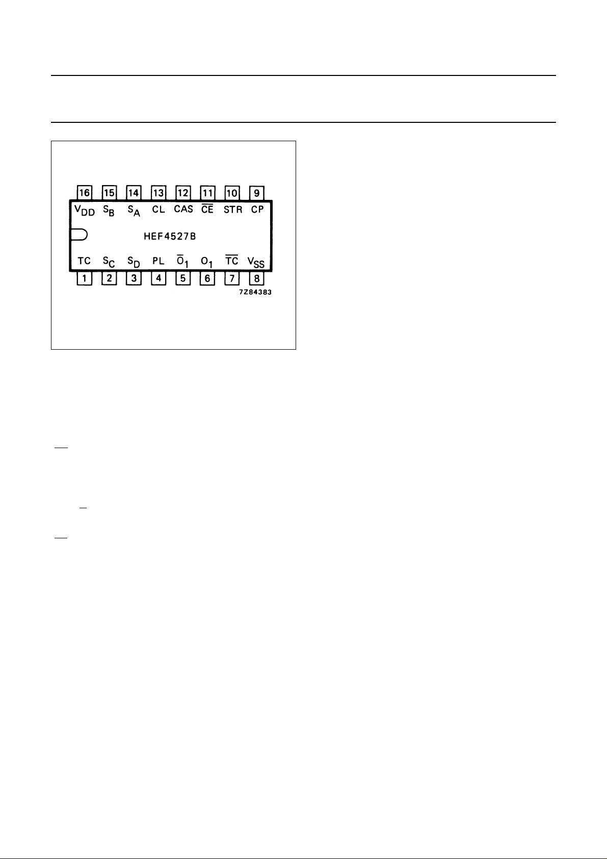
Fig.2 Pinning diagram.
HEF4527B
MSI
HEF4527BP(N): 16-lead DIL; plastic
(SOT38-1)
HEF4527BD(F): 16-lead DIL; ceramic (cerdip)
(SOT74)
HEF4527BT(D): 16-lead SO; plastic
(SOT109-1)
( ): Package Designator North America
PINNING
CP clock input
PL preset to ‘9’ input
CL counter clear input
CE count enable input (active LOW)
STR strobe input
CAS cascade input
S
to S
A
D
O
to O
1
TC terminal count output (active HIGH)
TC terminal count output (active LOW)
rate select inputs
rate outputs
1
January 1995 3
 Loading...