

Philips HEF4517BU, HEF4517BT, HEF4517BPB, HEF4517BP, HEF4517BD Datasheet

DATA SH EET
Product specification
File under Integrated Circuits, IC04
January 1995
INTEGRATED CIRCUITS
HEF4517B
LSI
Dual 64-bit static shift register
For a complete data sheet, please also download:
•The IC04 LOCMOS HE4000B Logic
Family Specifications HEF, HEC
•The IC04 LOCMOS HE4000B Logic
Package Outlines/Information HEF, HEC
January 1995 2
Philips Semiconductors Product specification
Dual 64-bit static shift register
HEF4517B
LSI
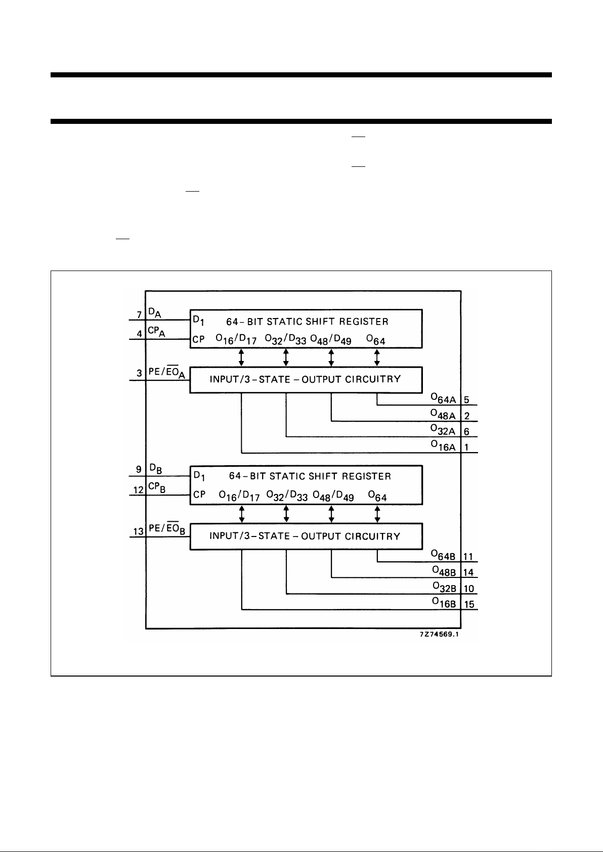
DESCRIPTION
The HEF4517B consists of two identical, independent
64-bit static shift registers. Each register has separate
clock (CP), data input (D), parallel
input-enable/output-enable (PE/EO) and four 3-state
outputs of the 16th, 32nd, 48th and 64th bit positions
(O16to O64). Data at the D input is entered into the first bit
on the LOW to HIGH transition of the clock, regardless of
the state of PE/EO.
When PE/
EO is LOW the outputs are enabled and the
device is in the 64-bit serial mode.
When PE/EO is HIGH the outputs are disabled (high
impedance OFF-state), the 64-bit shift register is divided
into four 16-bit shift registers with D, O16, O32and O48as
data inputs of the 1st, 17th, 33rd, and 49th bit respectively.
Schmitt-trigger action in the clock input makes the circuit
highly tolerant to slower clock rise and fall times.
FAMILY DATA, I
DD
LIMITS category LSI
See Family Specifications
Fig.1 Functional diagram.
January 1995 3
Philips Semiconductors Product specification
Dual 64-bit static shift register
HEF4517B
LSI
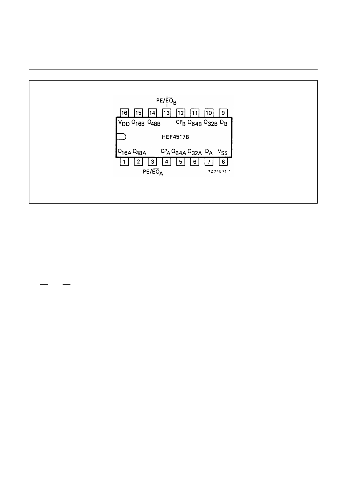
PINNING
HEF4517BP(N): 16-lead DIL; plastic (SOT38-1)
HEF4517BD(F): 16-lead DIL; ceramic (cerdip) (SOT74)
HEF4517BT(D): 16-lead SO; plastic (SOT109-1)
( ): Package Designator North America
CP
A
, CP
B
clock inputs
PE/
EOA, PE/EO
B
parallel input-enable/output-enable inputs
D
A
, D
B
data inputs
O
16A
, O
32A
, O
48A
3-state outputs/inputs
O
16B
, O
32B
, O
48B
3-state outputs/inputs
O
64A
, O
64B
3-state outputs
Fig.2 Pinning diagram.
 Loading...