

Page 1

查询HEF4104B供应商查询HEF4104B供应商
INTEGRATED CIRCUITS
DATA SH EET
For a complete data sheet, please also download:
•The IC04 LOCMOS HE4000B Logic
Family Specifications HEF, HEC
•The IC04 LOCMOS HE4000B Logic
Package Outlines/Information HEF, HEC
HEF4104B
MSI
Quadruple low to high voltage
translator with 3-state outputs
Product specification
File under Integrated Circuits, IC04
January 1995
Page 2
Philips Semiconductors Product specification
Quadruple low to high voltage translator
with 3-state outputs
DESCRIPTION
The HEF4104B quadruple low voltage to high voltage
translator with 3-state outputs provides the capability of
interfacing low voltage circuits to high voltage circuits,
such as low voltage LOCMOS and TTL to high voltage
LOCMOS. It has four data inputs (I0to I3), an active HIGH
output enable input (EO), four data outputs (O0to O3) and
their complements (O0to O3).
With EO HIGH, O0to O3and O0to O3are in the low
impedance ON-state, either HIGH or LOW as determined
to I3; with EO LOW, O0to O3and O0to O3are in the
by I
0
high impedance OFF-state.
HEF4104B
MSI
DDO
) and
SS
DDO
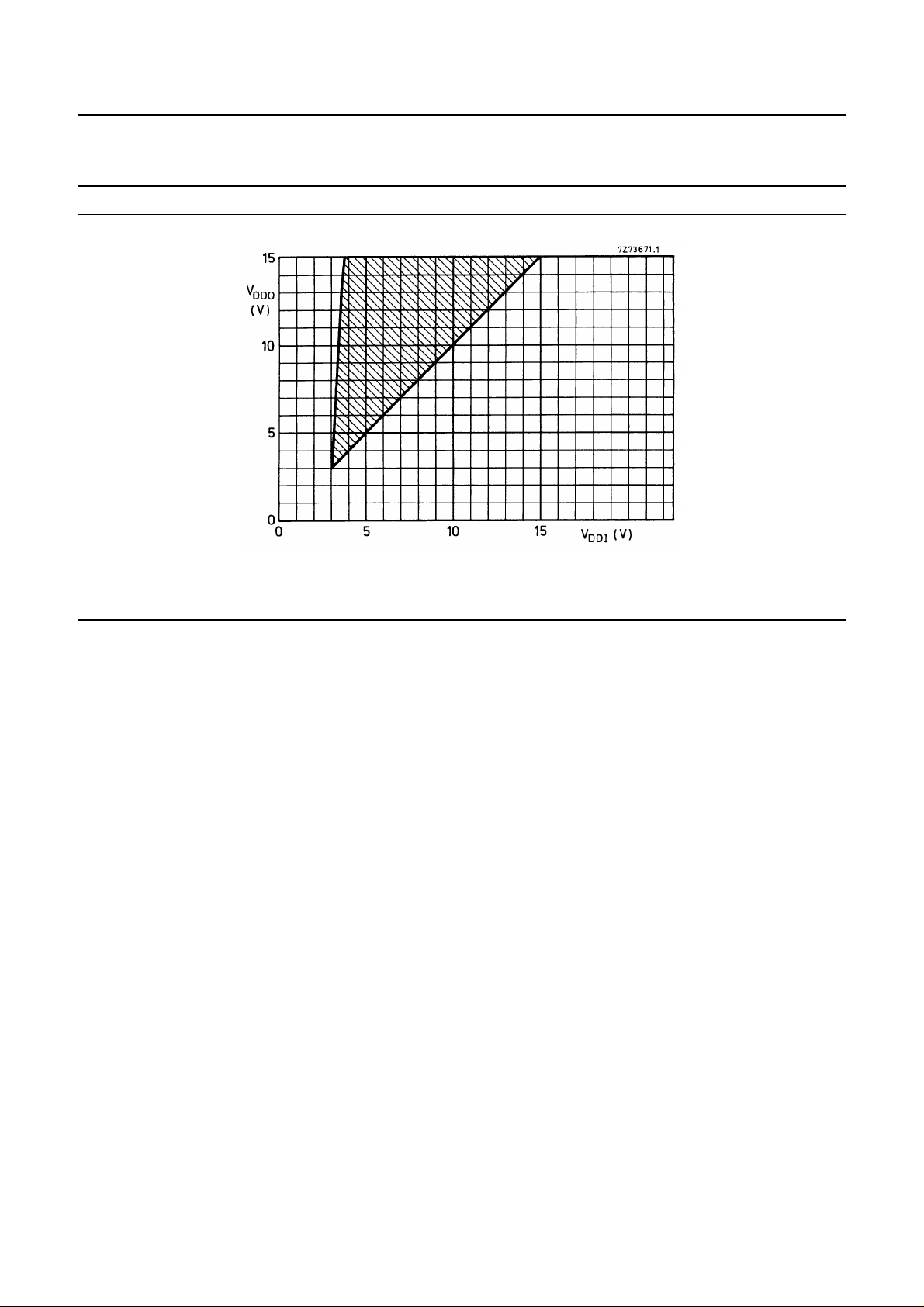
see graph
The device uses a common negative supply (V
separate positive supplies for inputs (V
(V
). V
DD0
must always be less than or equal to V
DDI
) and outputs
DDI
even during power turn-on and turn-off. For the
permissible operating range of V
DDI
and V
Fig.4.
Each input protection circuit is terminated between
V
and VSS. This allows the input signals to be driven
DDO
from any potential between V
and VSS, without regard
DDO
to current limiting. When driving from potentials greater
than V
or less than VSS, the current at each input must
DDO
be limited to 10 mA.
,
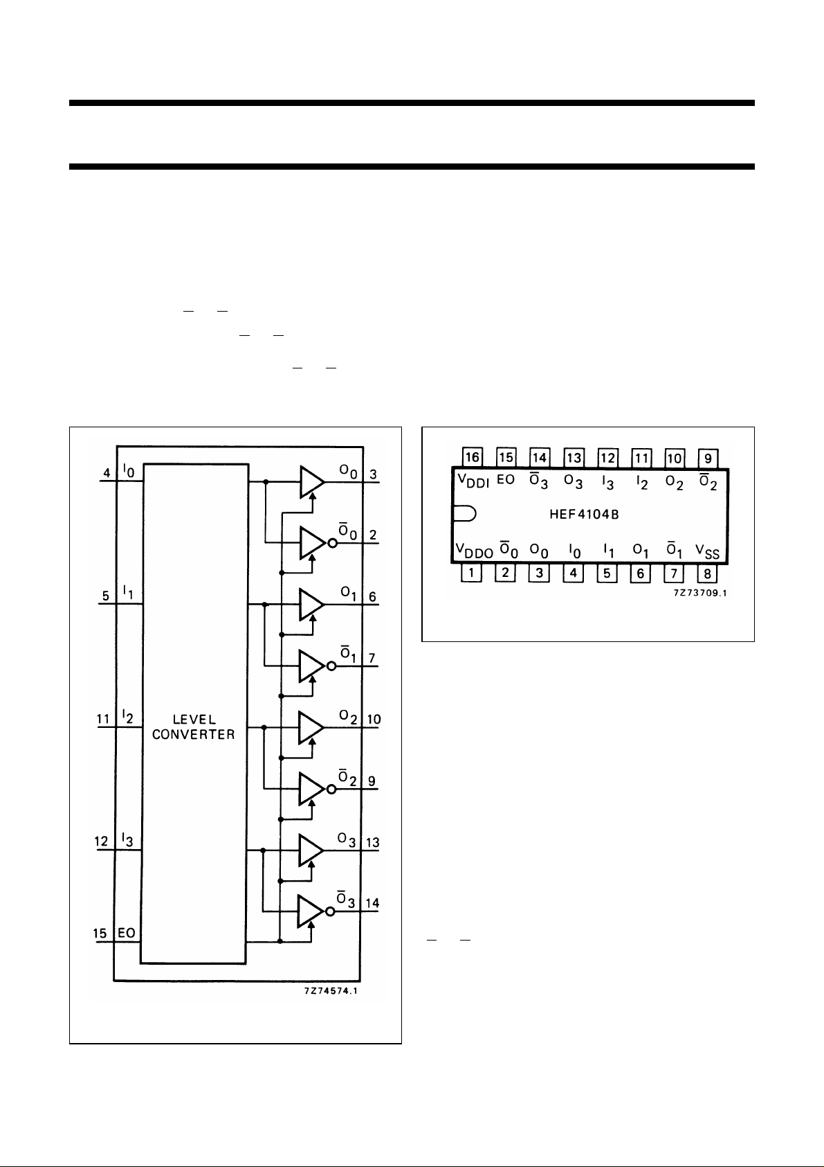
Fig.1 Functional diagram.
Fig.2 Pinning diagram.
HEF4104BP(N): 16-lead DIL; plastic
(SOT38-1)
HEF4104BD(F): 16-lead DIL; ceramic (cerdip)
(SOT74)
HEF4104BT(D): 16-lead SO; plastic
(SOT109-1)
( ): Package Designator North America
PINNING
I
to I
0
3
data inputs
EO output enable input
O
to O
0
3
O0to O
3
FAMILY DATA, I
data outputs
complementary data outputs
LIMITS category MSI
DD
See Family Specifications
January 1995 2
Page 3
Philips Semiconductors Product specification
Quadruple low to high voltage translator
with 3-state outputs
HEF4104B
MSI
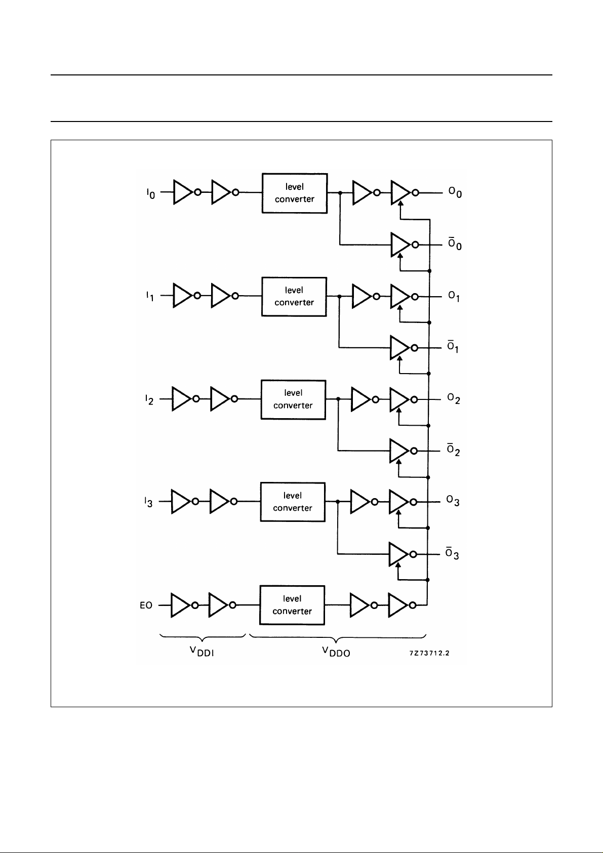
Fig.3 Logic diagram.
January 1995 3
Page 4
Philips Semiconductors Product specification
Quadruple low to high voltage translator
HEF4104B
with 3-state outputs
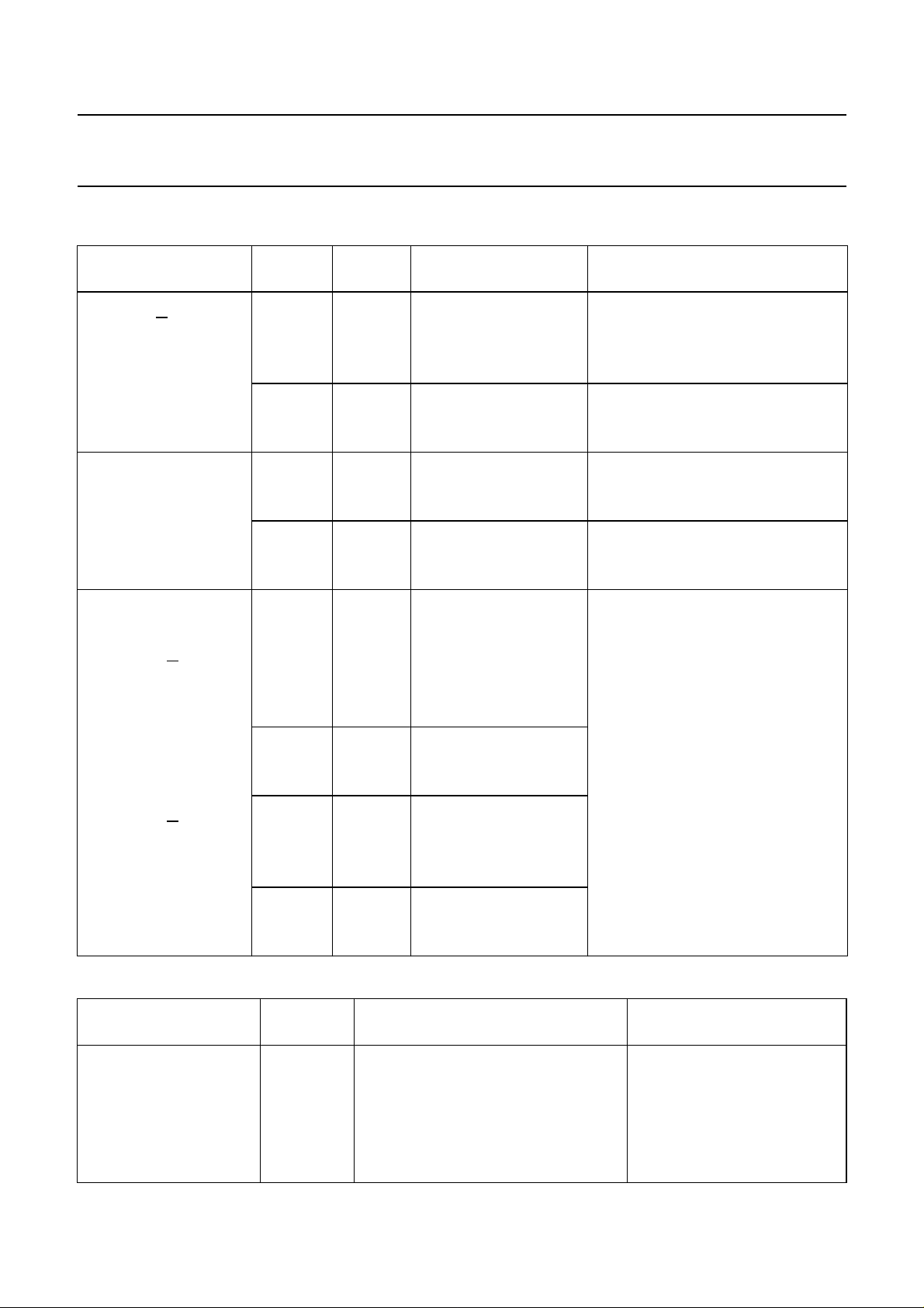
AC CHARACTERISTICS
V
= 0 V; T
SS
Propagation delays
In→ On, O
HIGH to LOW 10 t
LOW to HIGH 10 t
Output transition times 5 60 120 ns 10 ns + (1,0 ns/pF) C
HIGH to LOW 10 t
LOW to HIGH 10 t
3-state propagation
delays
Output disable times
EO → O
HIGH 10 t
LOW 10 t
Output enable times
EO → O
HIGH 10 t
LOW 10 t
=25°C; CL= 50 pF; input transition times ≤ 20 ns
amb
V
DD
V
n
SYMBOL TYP. MAX.
5 170 340 ns 143 ns + (0,55 ns/pF) C
PHL
15 65 135 ns 57 ns + (0,16 ns/pF) C
5 170 340 ns 143 ns + (0,55 ns/pF) C
PLH
15 70 140 ns 62 ns + (0,16 ns/pF) C
THL
15 20 40 ns 6 ns + (0,28 ns/pF) C
5 60 120 ns 10 ns + (1,0 ns/pF) C
TLH
15 20 40 ns 6 ns + (0,28 ns/pF) C
n
, O
n
5 70 135 ns
PHZ
15 60 120 ns
5 70 135 ns
PLZ
15 55 110 ns
n
, O
n
5 195 395 ns
PZH
15 80 165 ns
5 195 395 ns
PZL
15 80 160 ns
TYPICAL EXTRAPOLATION
FORMULA
80 160 ns 69 ns + (0,23 ns/pF) C
80 160 ns 69 ns + (0,23 ns/pF) C
30 60 ns 9 ns + (0,42 ns/pF) C
30 60 ns 9 ns + (0,42 ns/pF) C
55 110 ns
55 105 ns
95 195 ns
95 190 ns
MSI
L
L
L
L
L
L
L
L
L
L
L
L
V
DD
V
TYPICAL FORMULA FOR P (µW)
Dynamic power 5 3 000 f
dissipation per 10 12 200 f
package (P) 15 31 000 f
January 1995 4
+∑(foCL) × V
i
+∑(foCL) × V
i
+∑(foCL) × V
i
DD
DD
DD
2
2
2
where
fi= input freq. (MHz)
fo= output freq. (MHz)
C
= load capacitance (pF)
L
∑ (f
) = sum of outputs
oCL
V
= supply voltage (V)
DD
Page 5
Philips Semiconductors Product specification
Quadruple low to high voltage translator
with 3-state outputs
HEF4104B
MSI
Fig.4 V
as a function of V
DDO
; the shaded area shows the permissible operating range.
DDI
January 1995 5
 Loading...