Philips hef4031b DATASHEETS

INTEGRATED CIRCUITS
DATA SH EET
For a complete data sheet, please also download:
•The IC04 LOCMOS HE4000B Logic
Family Specifications HEF, HEC
•The IC04 LOCMOS HE4000B Logic
Package Outlines/Information HEF, HEC
HEF4031B
MSI
64-stage static shift register
Product specification
File under Integrated Circuits, IC04
January 1995

Philips Semiconductors Product specification
64-stage static shift register
DESCRIPTION
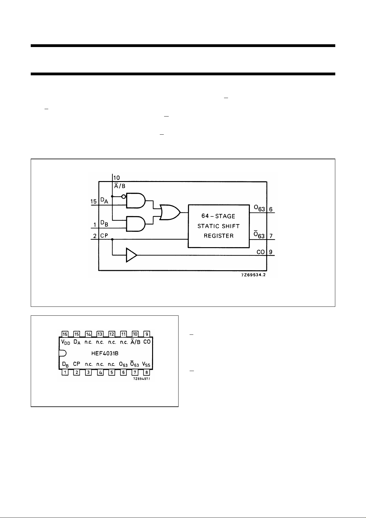
The HEF4031B is an edge-triggered 64-stage static shift
register with two serial data inputs (DA, DB), a data select
input A/B, a clock input (CP), a buffered clock output (CO),
and buffered outputs from the 64th bit position (O63, O63).
The output O63 is capable of driving one TTL load.
Data from DA or DB, as determined by the state of A/B, is
shifted into the first shift register position and all the data in
HEF4031B
MSI
the register is shifted one position to the right on the LOW
to HIGH transition of CP. D
by a HIGH on A/B. Registers can be cascaded either by
connecting all CP inputs together or by driving CP of the
most right-hand register with the system clock and
connecting CO to CP of the preceding register. When the
second technique is used in the recirculating mode, a
flip-flop must be used to store O63 of the most right-hand
register until the most left-hand register is clocked.
is selected by a LOW, and D
A
B
Fig.1 Functional diagram.
Fig.2 Pinning diagram.
HEF4031BP(N): 16-lead DIL; plastic (SOT38-1)
HEF4031BD(F): 16-lead DIL; ceramic (cerdip) (SOT74)
HEF4031BT(D): 16-lead SO; plastic (SOT109-1)
( ): Package Designator North America
PINNING
D
, DBdata inputs
A
A/B data select input
CP clock input (LOW to HIGH edge-triggered)
CO buffered clock output
O
63
O
63
FAMILY DATA, I
See Family Specifications
buffered output from the 64th stage
complementary buffered output from the 64th
stage
LIMITS category MSI
DD
January 1995 2

Philips Semiconductors Product specification
64-stage static shift register
HEF4031B
MSI
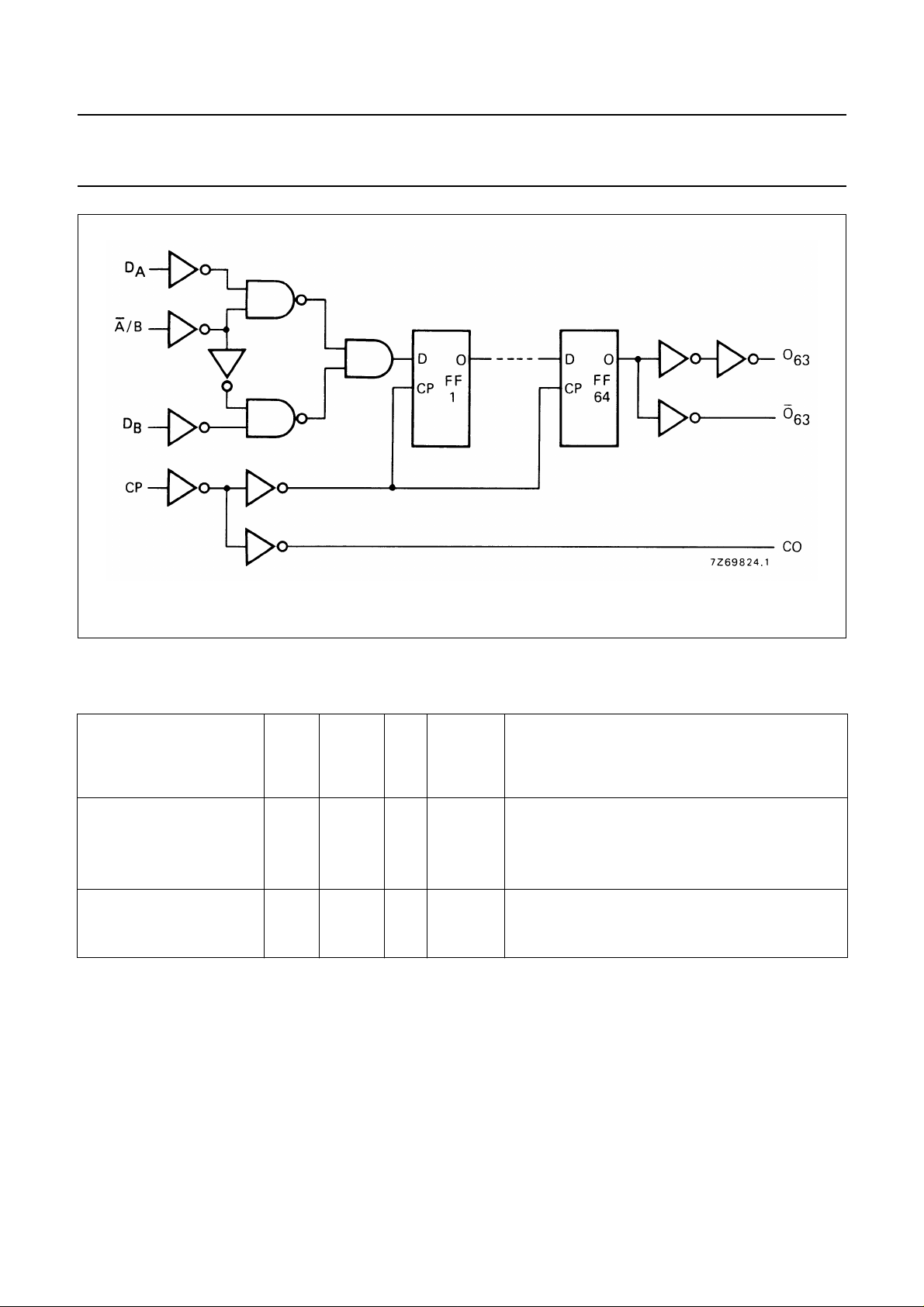
Fig.3 Logic diagram.
DC CHARACTERISTICS
V
= 0 V; VI=VSSor V
SS
DD
T
(°c)
amb
V
DD
V
V
OH
V
V
V
OL
SYMBOL
−40 + 25 + 85
MIN. MAX. MIN. MAX. MIN. MAX.
Output (source) 5 4, 6 1,0 0,85 0,65 mA
current 10 9,5 −I
HIGH; O
HIGH; O
63
63
15 13,5 10,0 8,5 6,5 mA
5 2,5 −I
OH
OH
3,0 2,5 2,0 mA
3,0 2,5 2,0 mA
Output (sink) 4,75 0,4 2,7 2,3 1,8 mA
current 10 0,5 I
LOW; O
63
15 1,5 24,0 20,0 16,0 mA
OL
9,5 8,0 6,3 mA
January 1995 3
 Loading...