

Philips HEF40175BU, HEF40175BT, HEF40175BPB, HEF40175BP, HEF40175BDB Datasheet
...
DATA SH EET
Product specification
File under Integrated Circuits, IC04
January 1995
INTEGRATED CIRCUITS
HEF40175B
MSI
Quadruple D-type flip-flop
For a complete data sheet, please also download:
•The IC04 LOCMOS HE4000B Logic
Family Specifications HEF, HEC
•The IC04 LOCMOS HE4000B Logic
Package Outlines/Information HEF, HEC
January 1995 2
Philips Semiconductors Product specification
Quadruple D-type flip-flop
HEF40175B
MSI
DESCRIPTION
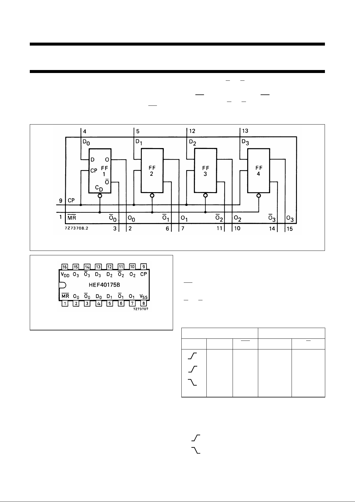
The HEF40175B is a quadruple edge-triggered D-type
flip-flop with four data inputs (D0to D3), a clock input (CP),
an overriding asynchronous master reset input (MR), four
buffered outputs (O0to O3), and four complementary
buffered outputs (
O0to O3). Information on D0to D3is
transferred to O0to O3on the LOW to HIGH transition of
CP if MR is HIGH. When LOW, MR resets all flip-flops
(O0to O3= LOW, O0to O3= HIGH), independent of CP
and D0to D3.
Fig.1 Functional diagram.
FAMILY DATA, IDDLIMITS category MSI
See Family Specifications
HEF40175BP(N): 16-lead DIL; plastic
(SOT38-1)
HEF40175BD(F): 16-lead DIL; ceramic (cerdip)
(SOT74)
HEF40175BT(D): 16-lead SO; plastic
(SOT109-1)
( ): Package Designator North America
Fig.2 Pinning diagram.
PINNING
FUNCTION TABLE
Notes
1. H = HIGH state (the more positive voltage)
L = LOW state (the less positive voltage)
X = state is immaterial
= positive-going transition
= negative-going transition
D
0
to D3data inputs
CP clock input (LOW to HIGH; edge-triggered)
MR master reset input (active LOW)
O
0
to O3buffered outputs
O0to O3complementary buffered outputs
INPUTS OUTPUTS
CP D
MR O O
HH H L
LH L H
X H no change no change
XXL L H
 Loading...