

Philips hef4016b DATASHEETS

INTEGRATED CIRCUITS
DATA SH EET
For a complete data sheet, please also download:
•The IC04 LOCMOS HE4000B Logic
Family Specifications HEF, HEC
•The IC04 LOCMOS HE4000B Logic
Package Outlines/Information HEF, HEC
HEF4016B
gates
Quadruple bilateral switches
Product specification
File under Integrated Circuits, IC04
January 1995
Philips Semiconductors Product specification
Quadruple bilateral switches
DESCRIPTION
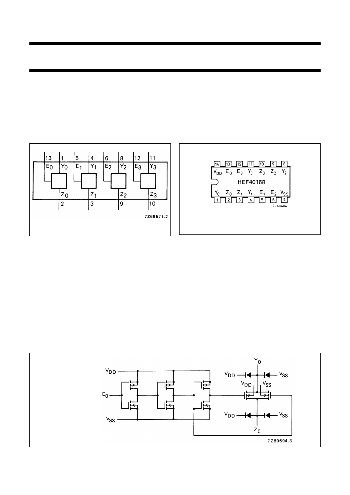
The HEF4016B has four independent analogue switches
(transmission gates). Each switch has two input/output
terminals (Y/Z) and an active HIGH enable input (E). When
E is connected to VDDa low impedance bidirectional path
between Y and Z is established (ON condition). When E is
connected to VSSthe switch is disabled and a high
HEF4016B
gates
impedance between Y and Z is established (OFF
condition). Current through a switch will not cause
additional V
terminals of the switch is maintained within the supply
voltage range; VDD≥ (VY, VZ) ≥ VSS. Inputs Y and Z are
electrically equivalent terminals.
current provided the voltage at the
DD
Fig.1 Functional diagram.
PINNING
to E
E
0
Y
to Y
0
to Z
Z
0
enable inputs
3
input/output terminals
3
input/output terminals
3
APPLICATION INFORMATION
Some examples of applications for the HEF4016B are:
• Signal gating
• Modulation
• Demodulation
• Chopper
Fig.2 Pinning diagram.
HEF4016BP(N): 14-lead DIL; plastic (SOT27-1)
HEF4016BD(F): 14-lead DIL; ceramic (cerdip) (SOT73)
HEF4016BT(D): 14-lead SO; plastic (SOT108-1)
( ): Package Designator North America
Fig.3 Schematic diagram
(one switch).
January 1995 2
Philips Semiconductors Product specification
Quadruple bilateral switches
HEF4016B
RATINGS
Limiting values in accordance with the Absolute Maximum System (IEC 134)
Power dissipation per switch P max. 100 mW
For other RATINGS see Family Specifications
DC CHARACTERISTICS
=25°C; VSS= 0 V (unless otherwise specified)
T
amb
V
PARAMETER
DD
V
5 8000 −ΩE
ON resistance 10 R
15 115 350 Ω
5 140 425 Ω Enat VIH; Vis=VSS; see Fig.4
ON resistance 10 R
15 50 145 Ω
5 170 515 Ω Enat VIH; Vis=VDD; see Fig.4
ON resistance 10 R
15 75 220 Ω
‘∆’ ON resistance 5 200 −ΩE
between any two 10 ∆R
channels 15 10 −Ω
SYMBOL TYP. MAX. UNIT CONDITIONS
at VIH; Vis= 0 to VDD; see Fig.4
n
ON
ON
ON
ON
230 690 Ω
65 195 Ω
95 285 Ω
15 −Ω
at VIH; Vis= 0 to VDD; see Fig.4
n
gates
T
(°C)
amb
UNIT−40 + 25 + 85 CONDITION
PARAMETER
V
DD
V SYMBOL
MIN. MAX. MIN. MAX. MIN. MAX.
Quiescent 5 − 1,0 − 1,0 − 7,5 µAV
device 10 I
DD
− 2,0 − 2,0 − 15,0 µA
current 15 − 4,0 − 4,0 − 30,0 µA
Input leakage
current at E
n
15 ± I
IN
−−−300 − 1000
nA E
= 0; all valid
SS
input combinations;
VI=VSSor V
at VSSor V
n
OFF-state leakage 5 −−−−−−nA Enat VIL;
current, any 10 I
OZ
−−−−−−nA
channel OFF 15 −−−200 −−nA
input 5 − 1,5 − 1,5 − 1,5 V switch OFF; see
E
n
voltage LOW 10 V
IL
− 3,0 − 3,0 − 3,0 V
Vis=VSSor VDD;
Vos=VDDor V
Fig.9 for I
15 − 4,0 − 4,0 − 4,0 V
E
input 5 3,5 − 3,5 − 3,5 − V low-impedance
n
voltage HIGH 10 V
15 11,0 − 11,0 − 11,0 − V
IH
7,0 − 7,0 − 7,0 − V
between Y and Z (ON
condition)
see RONswitch
DD
DD
SS
OZ
January 1995 3
 Loading...