

Philips HEF4011UBU, HEF4011UBPB, HEF4011UBP, HEF4011UBDB, HEF4011UBD Datasheet

DATA SH EET
Product specification
File under Integrated Circuits, IC04
January 1995
INTEGRATED CIRCUITS
HEF4011UB
gates
Quadruple 2-input NAND gate
For a complete data sheet, please also download:
•The IC04 LOCMOS HE4000B Logic
Family Specifications HEF, HEC
•The IC04 LOCMOS HE4000B Logic
Package Outlines/Information HEF, HEC
January 1995 2
Philips Semiconductors Product specification
Quadruple 2-input NAND gate
HEF4011UB
gates
DESCRIPTION
The HEF4011UB is a quadruple 2-input NAND gate. This
unbuffered single stage version provides a direct
implementation of the NAND function. The output
impedance and output transition time depends on the input
voltage and input rise and fall times applied.
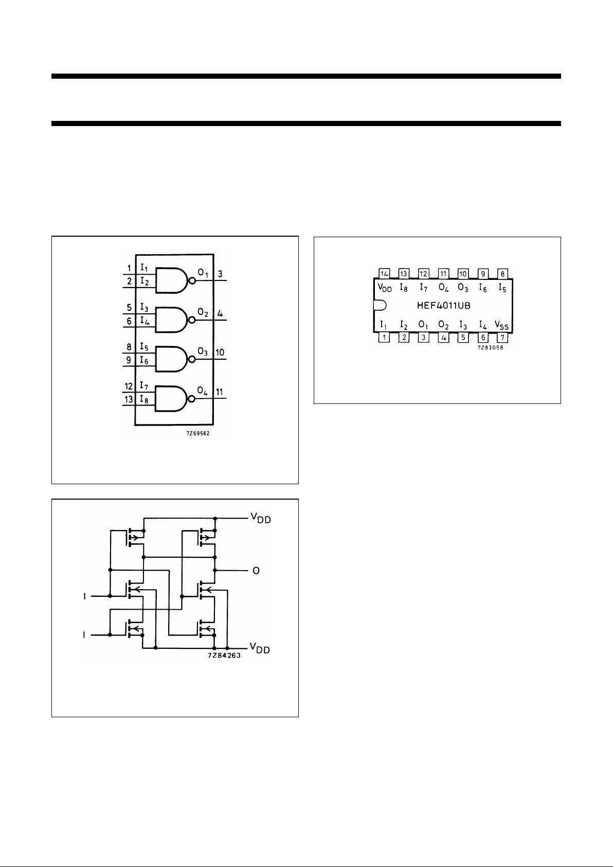
Fig.1 Functional diagram.
HEF4011UBP(N): 14-lead DIL; plastic
(SOT27-1)
HEF4011UBD(F): 14-lead DIL; ceramic (cerdip)
(SOT73)
HEF4011UBT(D): 14-lead SO; plastic
(SOT108-1)
( ): Package Designator North America
Fig.2 Pinning diagram.
FAMILY DATA, IDDLIMITS category GATES
See Family Specifications for V
IH/VIL
unbuffered stages
Fig.3 Schematic diagram (one gate). The
splitting-up of the n-transistors provide
identical inputs.

January 1995 3
Philips Semiconductors Product specification
Quadruple 2-input NAND gate
HEF4011UB
gates
AC CHARACTERISTICS
V
SS
= 0 V; T
amb
=25°C; CL= 50 pF; input transition times ≤20 ns
V
DD
V
SYMBOL TYP. MAX.
TYPICAL EXTRAPOLATION
FORMULA
Propagation delays
In→ O
n
5 60 120 ns 25 ns + (0,70 ns/pF) C
L
HIGH to LOW 10 t
PHL
25 50 ns 12 ns + (0,27 ns/pF) C
L
15 20 40 ns 10 ns + (0,20 ns/pF) C
L
5 35 70 ns 8 ns + (0,55 ns/pF) C
L
LOW to HIGH 10 t
PLH
20 40 ns 9 ns + (0,23 ns/pF) C
L
15 17 35 ns 9 ns + (0,16 ns/pF) C
L
Output transition 5 75 150 ns 15 ns + (1,20 ns/pF) C
L
times 10 t
THL
30 60 ns 6 ns + (0,48 ns/pF) C
L
HIGH to LOW 15 20 40 ns 4 ns + (0,32 ns/pF) C
L
5 60 110 ns 10 ns + (1,00 ns/pF) C
L
LOW to HIGH 10 t
TLH
30 60 ns 9 ns + (0,42 ns/pF) C
L
15 20 40 ns 6 ns + (0,28 ns/pF) C
L
Input capacitance C
IN
10 pF
V
DD
V
TYPICAL FORMULA FOR P (µW)
Dynamic power 5 500 f
i
+∑(foCL) × V
DD
2
where
dissipation per 10 5 000 f
i
+∑(foCL) × V
DD
2
fi= input freq. (MHz)
package (P) 15 25 000 f
i
+∑(foCL) × V
DD
2
fo= output freq. (MHz)
C
L
= load capacitance (pF)
∑ (f
oCL
) = sum of outputs
V
DD
= supply voltage (V)
 Loading...