Philips hef4011ub DATASHEETS

INTEGRATED CIRCUITS
DATA SH EET
For a complete data sheet, please also download:
•The IC04 LOCMOS HE4000B Logic
Family Specifications HEF, HEC
•The IC04 LOCMOS HE4000B Logic
Package Outlines/Information HEF, HEC
HEF4011UB
gates
Quadruple 2-input NAND gate
Product specification
File under Integrated Circuits, IC04
January 1995

Philips Semiconductors Product specification
Quadruple 2-input NAND gate
DESCRIPTION
The HEF4011UB is a quadruple 2-input NAND gate. This
unbuffered single stage version provides a direct
implementation of the NAND function. The output
impedance and output transition time depends on the input
voltage and input rise and fall times applied.
HEF4011UB
gates
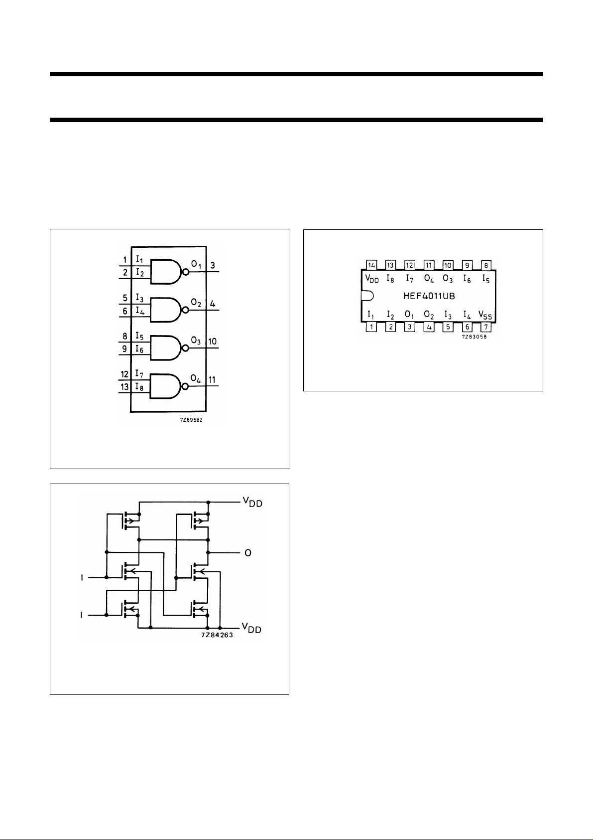
Fig.2 Pinning diagram.
Fig.1 Functional diagram.
Fig.3 Schematic diagram (one gate). The
splitting-up of the n-transistors provide
identical inputs.
HEF4011UBP(N): 14-lead DIL; plastic
(SOT27-1)
HEF4011UBD(F): 14-lead DIL; ceramic (cerdip)
(SOT73)
HEF4011UBT(D): 14-lead SO; plastic
(SOT108-1)
( ): Package Designator North America
FAMILY DATA, IDDLIMITS category GATES
See Family Specifications for V
January 1995 2
unbuffered stages
IH/VIL

Philips Semiconductors Product specification
Quadruple 2-input NAND gate
HEF4011UB
AC CHARACTERISTICS
V
= 0 V; T
SS
Propagation delays
In→ O
HIGH to LOW 10 t
LOW to HIGH 10 t
Output transition 5 75 150 ns 15 ns + (1,20 ns/pF) C
times 10 t
HIGH to LOW 15 20 40 ns 4 ns + (0,32 ns/pF) C
LOW to HIGH 10 t
Input capacitance C
=25°C; CL= 50 pF; input transition times ≤20 ns
amb
V
DD
V
n
5 60 120 ns 25 ns + (0,70 ns/pF) C
SYMBOL TYP. MAX.
PHL
15 20 40 ns 10 ns + (0,20 ns/pF) C
5 35 70 ns 8 ns + (0,55 ns/pF) C
PLH
15 17 35 ns 9 ns + (0,16 ns/pF) C
THL
5 60 110 ns 10 ns + (1,00 ns/pF) C
TLH
15 20 40 ns 6 ns + (0,28 ns/pF) C
IN
TYPICAL EXTRAPOLATION
FORMULA
25 50 ns 12 ns + (0,27 ns/pF) C
20 40 ns 9 ns + (0,23 ns/pF) C
30 60 ns 6 ns + (0,48 ns/pF) C
30 60 ns 9 ns + (0,42 ns/pF) C
10 pF
gates
L
L
L
L
L
L
L
L
L
L
L
L
V
DD
V
TYPICAL FORMULA FOR P (µW)
Dynamic power 5 500 f
dissipation per 10 5 000 f
package (P) 15 25 000 f
+∑(foCL) × V
i
+∑(foCL) × V
i
+∑(foCL) × V
i
DD
DD
DD
2
2
2
where
fi= input freq. (MHz)
fo= output freq. (MHz)
= load capacitance (pF)
C
L
∑ (f
) = sum of outputs
oCL
= supply voltage (V)
V
DD
January 1995 3
 Loading...