

Philips HEF40106BDB, HEF40106BD, HEF40106BU, HEF40106BT, HEF40106BPB Datasheet
...
DATA SH EET
Product specification
File under Integrated Circuits, IC04
January 1995
INTEGRATED CIRCUITS
HEF40106B
gates
Hex inverting Schmitt trigger
For a complete data sheet, please also download:
•The IC04 LOCMOS HE4000B Logic
Family Specifications HEF, HEC
•The IC04 LOCMOS HE4000B Logic
Package Outlines/Information HEF, HEC
January 1995 2
Philips Semiconductors Product specification
Hex inverting Schmitt trigger
HEF40106B
gates
DESCRIPTION
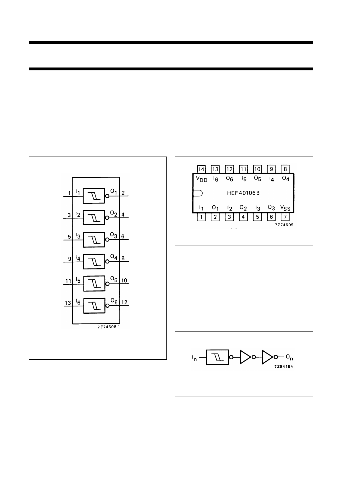
Each circuit of the HEF40106B functions as an inverter
with Schmitt-trigger action. The Schmitt-trigger switches at
different points for the positive and negative-going input
signals. The difference between the positive-going voltage
(VP) and the negative-going voltage (VN) is defined as
hysteresis voltage (VH).
This device may be used for enhanced noise immunity or
to “square up” slowly changing waveforms.
Fig.1 Functional diagram.
FAMILY DATA, IDDLIMITS category GATES
See Family Specifications
HEF40106BP(N): 14-lead DIL; plastic
(SOT27-1)
HEF40106BD(F): 14-lead DIL; ceramic (cerdip)
(SOT73)
HEF40106BT(D): 14-lead SO; plastic
(SOT108-1)
( ): Package Designator North America
Fig.2 Pinning diagram.
Fig.3 Logic diagram (one inverter).
January 1995 3
Philips Semiconductors Product specification
Hex inverting Schmitt trigger
HEF40106B
gates
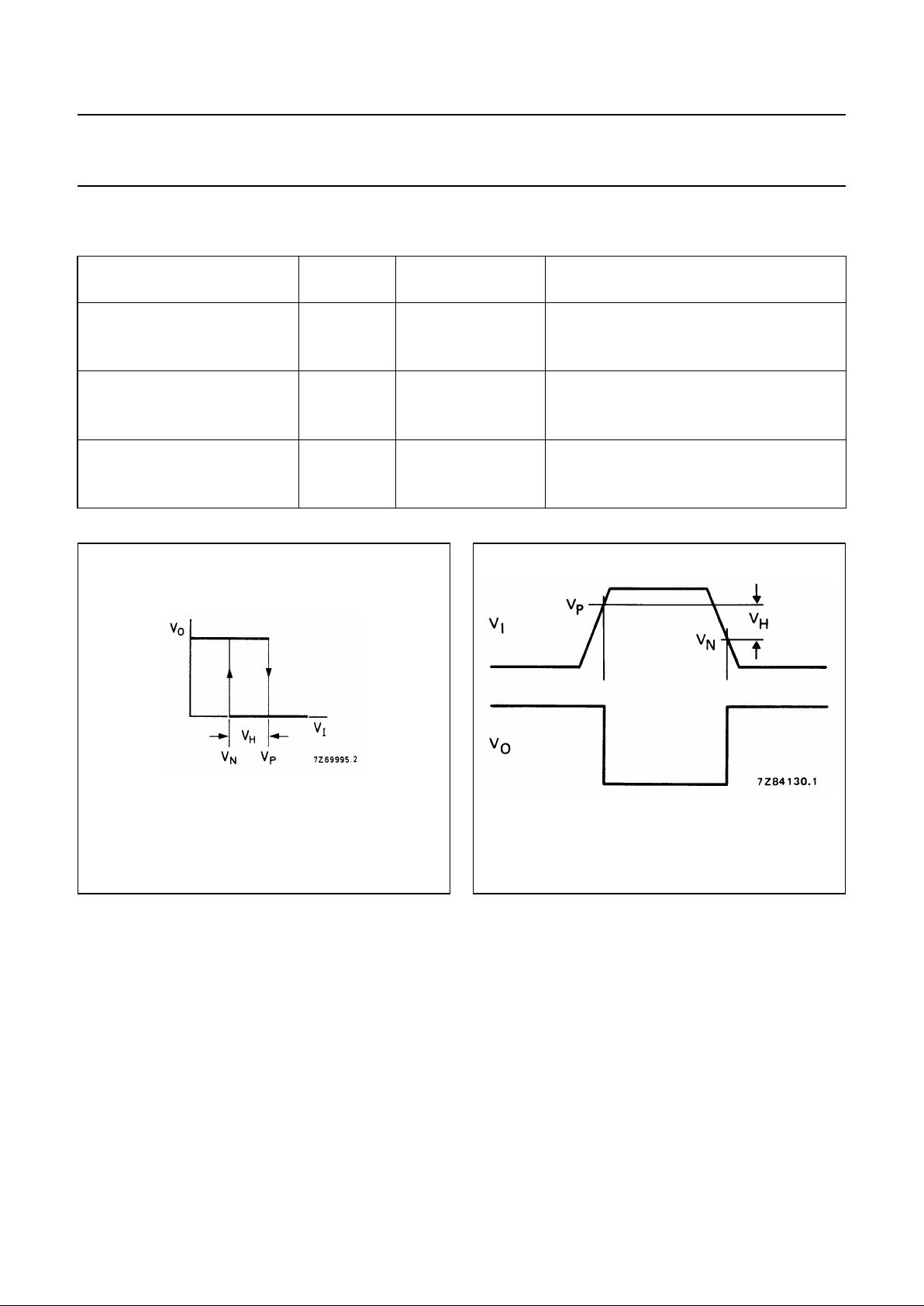
DC CHARACTERISTICS
V
SS
= 0 V; T
amb
=25°C
V
DD
V
SYMBOL MIN. TYP. MAX.
Hysteresis 5 0,5 0,8 V
voltage 10 V
H
0,7 1,3 V
15 0,9 1,8 V
Switching levels 5 2 3,0 3,5 V
positive-going 10 V
P
3,7 5,8 7 V
input voltage 15 4,9 8,3 11 V
negative-going 5 1,5 2,2 3 V
input voltage 10 V
N
3 4,5 6,3 V
15 4 6,5 10,1 V
Fig.4 Transfer characteristic.
Fig.5 Waveforms showing definition of
VP,VNand VH, where VNand VPare
between limits of 30% and 70%.
 Loading...