Philips hef4006b DATASHEETS

INTEGRATED CIRCUITS
DATA SH EET
For a complete data sheet, please also download:
•The IC04 LOCMOS HE4000B Logic
Family Specifications HEF, HEC
•The IC04 LOCMOS HE4000B Logic
Package Outlines/Information HEF, HEC
HEF4006B
MSI
18-stage static shift register
Product specification
File under Integrated Circuits, IC04
January 1995

Philips Semiconductors Product specification
18-stage static shift register
DESCRIPTION
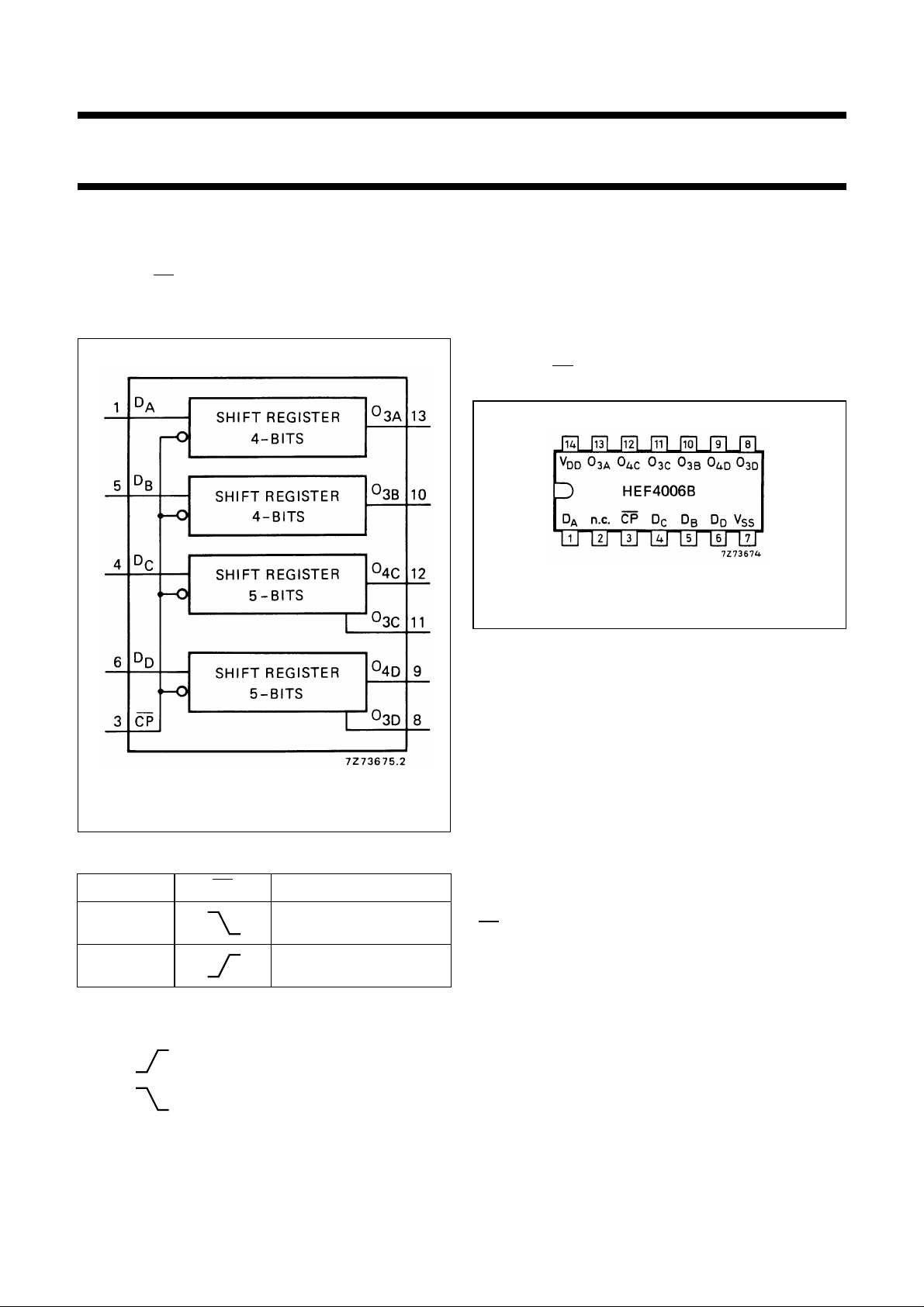
The HEF4006B is an 18-stage shift register arranged as
two 4-stage and two 5-stage shift registers with a common
clock input (CP). The two 4-stage shift registers each have
a data input (DA, DB) and a data output (O3A, O3B); the two
HEF4006B
MSI
5-stage shift registers each have a data input (D
data outputs from the fourth and fifth stages (O3C, O4C,
O3D, O4D).
The registers can be operated in parallel or interconnected
to form a single shift register of up to 18 bits. Data are
shifted into the first register position of each register from
the data inputs (DA to DD) and all the data in each register
are shifted one position to the right on the HIGH to LOW
transition of CP.
, DD) and
C
Fig.1 Functional diagram.
FUNCTION TABLE
D
n
D
1
CP O
X no change
Notes
1. X = state is immaterial
2. = positive-going transition
Fig.2 Pinning diagram.
HEF4006BP(N): 14-lead DIL; plastic
(SOT27-1)
HEF4006BD(F): 14-lead DIL; ceramic (cerdip)
(SOT73)
HEF4006BT(D): 14-lead SO; plastic
(SOT108-1)
( ): Package Designator North America
(5)
n
D
1
PINNING
D
A
to D
D
data inputs
CP clock input
(HIGH to LOW; edge-triggered)
to O3D; O4C; O4Ddata outputs
O
3A
FAMILY DATA, I
LIMITS category MSI
DD
See Family Specifications
3. = negative-going transition
4. D
= either HIGH or LOW
1
5. The moment D1 appears at O depends on the register
length.
January 1995 2
 Loading...