

Page 1
查询GTL2020供应商
INTEGRATED CIRCUITS
GTL2020/GTL2021/GTL2022/GTL2023
32-bit GTL terminator with octal enables
Product specification 2000 Jan 14
Page 2
Philips Semiconductors Product specification
32-bit GTL terminator with octal enables
FEATURES
•GTL2020 r
•GTL2021 r
•GTL2022 r
•GTL2023 r
•Low power: 50 µW
•Switching speed: 5 ns max.
•Channel on capacitance: 3 pF
•V
operating range: +5 V ±10%
CC
•Latch-up protection passes Class II JESD78
•ESD protection exceeds 2000 V HBM per JESD22-A114,
200 V MM per JESD22-A115, and 1000 V CDM per JESD22-C101
•Available in TSSOP56 package
DESCRIPTION
The GTL202x series are 32-bit bus switches with GTL termination
and octal output enables. The GTL202x is intended to provide GTL
bus termination in multi-processor environments.
The enable pins allow the system control to disconnect the bus
termination. When the bus switch is enabled, a 56, 75, 100 or 150 Ω
series resistance is connected to the GTL Vbias.
is 56 Ω typical connected to 1.5 V V
ON
is 75 Ω typical connected to 1.5 V V
ON
is 100 Ω typical connected to 1.5 V V
ON
is 150 Ω typical connected to 1.5 V V
ON
BIAS
BIAS
BIAS
BIAS
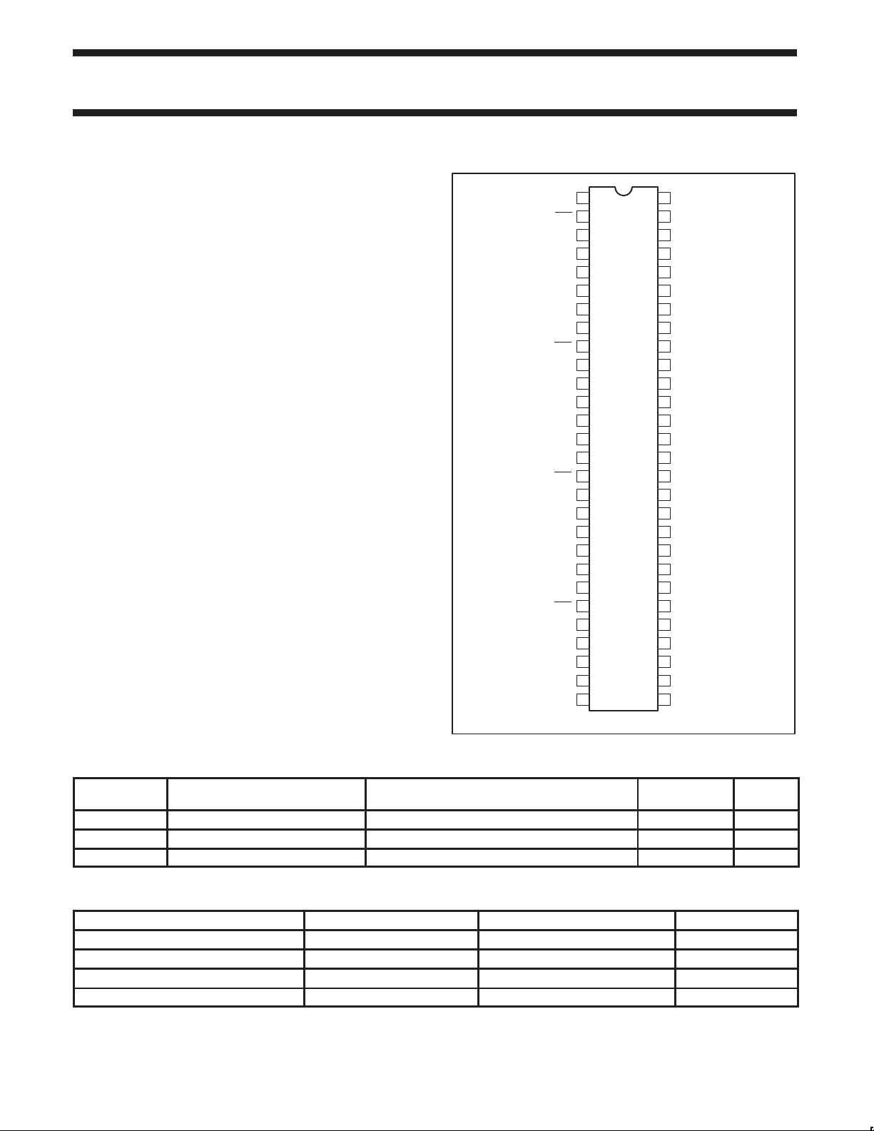
PIN CONFIGURATION
1
EN0
2
3
A0
4
A1
5
A2
6
A3
7
GND
VBIAS1A
VBIAS2A
VBIAS3A
8
9
EN1
10
A8
11
A9
12 45
13
14
GND
15
16
EN2
17
A16
18 39
A17
19 38
A18
20
21
GND
22
23
EN3
24
A24
25 32
26 31 A30A26
27 30 A31A27
28 29GND NC
GTL2020/GTL2021/
GTL2022/GTL2023
56VBIAS0A
V
CC
VBIAS0B
55
A4
54
A5
53
A6
52
A7
51
NC
50
V
49
CC
VBIAS1B
48
47
A12
46
A13
A14A10
A15
44A11
NC
43
42
V
CC
VBIAS2B
41
40
A20
A21
A22
37A19
A23
36
NC
35
V
CC
34
VBIAS3B
33
A28
A29A25
SW00473
QUICK REFERENCE DA TA
SYMBOL PARAMETER
t
PE/PD
C
ON
C
OFF
Bus enable/disable CL = 20 pF, RL = 500 Ω 2.5 nS
Input capacitance switch on VIN = 0 V 3 pF
Input capacitance switch off VIN = 0 V 6 pF
CONDITIONS
T
= 25°C; GND = 0V
amb
TYPICAL UNIT
ORDERING INFORMATION
PACKAGES TEMPERATURE RANGE ORDER CODE DWG NUMBER
56-Pin Plastic TSSOP Type II –40°C to +85°C GTL2020 DGG SOT364-1
56-Pin Plastic TSSOP Type II –40°C to +85°C GTL2021 DGG SOT364-1
56-Pin Plastic TSSOP Type II –40°C to +85°C GTL2022 DGG SOT364-1
56-Pin Plastic TSSOP Type II –40°C to +85°C GTL2023 DGG SOT364-1
2000 Jan 14
2
Page 3

Philips Semiconductors Product specification
SYMBOL
PARAMETER
TEST CONDITIONS
UNIT
32-bit GTL terminator with octal enables
LOGIC DIAGRAM
A0
A7
EN0
A8
A15
EN1
A16
A23
EN2
R
R
R
R
R
R
VBIAS0A
VBIAS0B
VBIAS1A
VBIAS1B
VBIAS2A
VBIAS2B
FUNCTION TABLE
ENn SWITCH
L ON
H OFF
NOTES:
When enabled:
Ports Ax connect to V
Ports Ay connect to V
Where:
X = 0–3, 8–11, 16–19, 24–27
Y = 4–7, 12–15, 20–23, 28–31
GTL2020/GTL2021/
GTL2022/GTL2023
BIASnA
BIASnB
A24
A31
EN3
R
R
VBIAS3A
VBIAS3B
SW00474
Figure 1.
ABSOLUTE MAXIMUM RATINGS
1
Above which the useful life may be impaired. For user guidelines, not tested.
SYMBOL
V
CC
V
I
T
stg
T
amb
Supply voltage to ground potentials Inputs and VCC only –0.5 to +7.0 V
DC input voltage –0.5 to +7.0 V
Storage temperature range –65 to +150 °C
Ambient temperature range with power applied –40 to +85 °C
PARAMETER CONDITIONS RATING UNIT
NOTE:
1. Stresses greater than those listed under Absolute Maximum Ratings may cause permanent damage to the device. this is a stress rating only
and functional operation of the device at these or any conditions above those indicated in the operational sections of this specification is not
implied. Exposure to absolute maximum rating conditions for extended periods of time may affect reliability.
RECOMMENDED OPERATING CONDITIONS
LIMITS
1
MAX.
V
V
V
V
V
V
BIAS
T
amb
IH
CC
IH
MIN. TYP.
TTL input HIGH voltage Control Inputs 2.0 — — V
IL
TTL input LOW voltage Control Inputs — — 0.8 V
DC supply voltage 4.5 — 5.5 V
High-level input voltage (control pin) 2.0 — — V
IL
Low-level input voltage (control pin) — — 0.8 V
DC supply voltage 1.35 — 1.65 V
Operating free-air temperature range –40 — +85 °C
2000 Jan 14
3
Page 4

Philips Semiconductors Product specification
SYMBOL
PARAMETER
TEST CONDITIONS
UNIT
I
r
SYMBOL
PARAMETER
WAVEFORM
TEST CONDITIONS
UNIT
GTL2020
GTL2021
GTL2022
GTL2023
32-bit GTL terminator with octal enables
DC ELECTRICAL CHARACTERISTICS
VCC = 5 V ±10%; T
I
V
IK
ON
C
IN
C
ON
C
OFF
I
CC
∆I
CC
NOTES:
1. Typical values are shown at V
2. This is the increase in supply current for each LVTTL input at the specified voltage level other than V
= –40°C to +85°C
amb
Control inputs VCC = 5.5 V, VI = VCC or GND — 0.1 ±1 µA
Switch inputs VCC = 5.5 V, VI = 1.65 V, V
= 0 V — 0.01 ±1 µA
BIAS
Input clamp voltage VCC = 4.5 V, IIK = –18 mA — –0.85 –1.2 V
GTL2020 switch on resistance VCC = MIN, VIN = 0 V, V
GTL2021 switch on resistance VCC = MIN, VIN = 0 V, V
GTL2022 switch on resistance VCC = MIN, VIN = 0 V, V
GTL2023 switch on resistance VCC = MIN, VIN = 0 V, V
= 1.5 V 42 56 70 Ω
BIAS
= 1.5 V 64 75 92 Ω
BIAS
= 1.5 V 80 100 120 Ω
BIAS
= 1.5 V 125 150 175 Ω
BIAS
Input capacitance ENx pins VIN = 0 V — 5.6 — pF
Input capacitance, switch on VIN = 0 V — 3 — pF
Input capacitance, switch off VIN = 0 V — 6 — pF
Power supply quiescent V
VCC = 4.5 V to 5.5 V; one input at VCC –3.0 V,
Additional supply current per input pin
= 5.0 V, +25°C ambient and maximum loading.
CC
2
= 1.5 OE = 0 V or V
BIAS
other inputs at VCC or GND
CC
GTL2020/GTL2021/
GTL2022/GTL2023
LIMITS
MIN. TYP.1MAX.
— — 10 µA
— 0.1 0.5 mA
or GND.
CC
AC ELECTRICAL CHARACTERISTICS
VCC = 5 V ±10%; T
t
PE
t
PD
t
PE
t
PD
t
PE
t
PD
t
PE
t
PD
= –40°C to +85°C; tr = tf = 2.5 nS
amb
Bus enable
Bus disable
Bus enable
Bus disable
Bus enable
Bus disable
Bus enable
Bus disable
AC WAVEFORMS
Input
Ax
1.5 V
t
PE
V
OL+0.3 V
VOLTAGE WAVEFORMS PROPAGATION DELAY TIMES
1.5 V
t
PD
Waveform 1.
3.0 V
0 V
V
OH–0.3 V
LIMITS
MIN. TYP. MAX.
1 CL = 20 pF, RL = 500 Ω 1 – 3 ns
1 CL = 20 pF, RL = 500 Ω 1 – 3 ns
1 CL = 20 pF, RL = 500 Ω 1 – 3 ns
1 CL = 20 pF, RL = 500 Ω 1 – 3 ns
1 CL = 20 pF, RL = 500 Ω 1 – 3 ns
1 CL = 20 pF, RL = 500 Ω 1 – 4 ns
1 CL = 20 pF, RL = 500 Ω 1 – 5 ns
1 CL = 20 pF, RL = 500 Ω 1 – 5 ns
TEST CIRCUIT
V
CC
V
O
C
L
of pulse generators.
OUT
V
OH
V
OL
SW00566
V
PULSE
GENERATOR
I
D.U.T.
R
T
Test Circuit for switching times
DEFINITIONS
RL = Load resistor
CL = Load capacitance includes jig and probe capacitance
RT = Termination resistance should be equal to Z
Figure 2.
20 pF
RL = 500Ω
SW00565
2000 Jan 14
4
Page 5

Philips Semiconductors Product specification
32-bit GTL terminator with octal enables
GTL2020/GTL2021/
GTL2022/GTL2023
TSSOP56: plastic thin shrink small outline package; 56 leads; body width 6.1mm SOT364-1
2000 Jan 14
5
Page 6

Philips Semiconductors Product specification
32-bit GTL terminator with octal enables
Data sheet status
Data sheet
status
Objective
specification
Preliminary
specification
Product
specification
Product
status
Development
Qualification
Production
Definition
This data sheet contains the design target or goal specifications for product development.
Specification may change in any manner without notice.
This data sheet contains preliminary data, and supplementary data will be published at a later date.
Philips Semiconductors reserves the right to make changes at any time without notice in order to
improve design and supply the best possible product.
This data sheet contains final specifications. Philips Semiconductors reserves the right to make
changes at any time without notice in order to improve design and supply the best possible product.
[1]
GTL2020/GTL2021/
GTL2022/GTL2023
[1] Please consult the most recently issued datasheet before initiating or completing a design.
Definitions
Short-form specification — The data in a short-form specification is extracted from a full data sheet with the same type number and title. For
detailed information see the relevant data sheet or data handbook.
Limiting values definition — Limiting values given are in accordance with the Absolute Maximum Rating System (IEC 134). Stress above one
or more of the limiting values may cause permanent damage to the device. These are stress ratings only and operation of the device at these or
at any other conditions above those given in the Characteristics sections of the specification is not implied. Exposure to limiting values for extended
periods may affect device reliability.
Application information — Applications that are described herein for any of these products are for illustrative purposes only. Philips
Semiconductors make no representation or warranty that such applications will be suitable for the specified use without further testing or
modification.
Disclaimers
Life support — These products are not designed for use in life support appliances, devices or systems where malfunction of these products can
reasonably be expected to result in personal injury . Philips Semiconductors customers using or selling these products for use in such applications
do so at their own risk and agree to fully indemnify Philips Semiconductors for any damages resulting from such application.
Right to make changes — Philips Semiconductors reserves the right to make changes, without notice, in the products, including circuits, standard
cells, and/or software, described or contained herein in order to improve design and/or performance. Philips Semiconductors assumes no
responsibility or liability for the use of any of these products, conveys no license or title under any patent, copyright, or mask work right to these
products, and makes no representations or warranties that these products are free from patent, copyright, or mask work right infringement, unless
otherwise specified.
Philips Semiconductors
811 East Arques Avenue
P.O. Box 3409
Sunnyvale, California 94088–3409
Telephone 800-234-7381
Copyright Philips Electronics North America Corporation 2000
All rights reserved. Printed in U.S.A.
Date of release: 02-00
Document order number: 9397 750 06869
2000 Jan 14
6
 Loading...