

Philips GTL2005 Datasheet

INTEGRATED CIRCUITS
GTL2005
Quad GTL/GTL+ to LVTTL/TTL
bidirectional non-latched translator
Product specification
Supersedes data of 1999 Jun 23
1999 Sep 17
Philips Semiconductors Product specification
SYMBOL
PARAMETER
UNIT
Quad GTL/GTL+ to LVTTL/TTL
bidirectional non-latched translator
FEA TURES
•Operates as a quad GTL/GTL+ sampling receiver or as a
LVTTL/TTL to GTL/GTL+ driver
•Quad bidirectional bus interface
•Live insertion/extraction permitted
•Latch-up protection exceeds 500 mA per JESD78
•ESD protection exceeds 2000 V HBM per JESD22-A114, and
1000 V CDM per JESD22-CC101
DESCRIPTION
The GTL2005 is a quad translating transceiver designed for 3.3 V
system interface with a GTL/GTL
The direction pin allows the part to function as either a GTL to TTL
sampling receiver or as a TTL to GTL interface.
QUICK REFERENCE DA TA
t
PLH
t
PHL
C
IN
C
I/O
+
bus.
Propagation delay
An to Bn or Bn to An
CL = 50 pF; VCC = 3.3 V
Input capacitance DIR VI = 0 V or V
I/O pin capacitance Outputs disabled; V
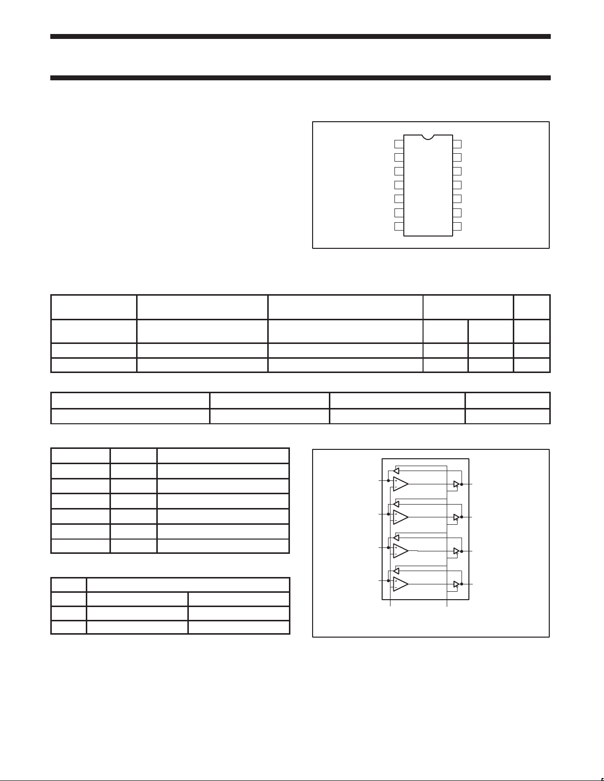
PIN CONFIGURATION
1DIR
2
A0
A1
3
4
GTLREF
A2
5
A3
6
GND
7
CONDITIONS TYPICAL
T
= 25°C B to A A to B
amb
CC
= 0 V or 3.0 V 7.8 4.5 pF
I/O
14
13
12
11
10
9
8
SW00321
2.1
1.9
3.0 3.0 pF
GTL2005
V
CC
B0
B1
GND
B2
B3
GND
4.1
4.3
ns
ORDERING INFORMATION
PACKAGES TEMPERATURE RANGE ORDER CODE DWG NUMBER
14-Pin Plastic TSSOP Type II –40°C to +85°C GTL2005 PW DH SOT402-1
PIN DESCRIPTION
LOGIC SYMBOL
PIN NUMBER SYMBOL NAME AND FUNCTION
1 DIR Direction control input
2, 3, 5, 6 A0 – A3 Data inputs/outputs (A side, GTL)
A0
B0
13, 12, 10, 9 B0 – B3 Data inputs/outputs (B side, TTL)
4 GTLREF GTL reference voltage
A1
B1
7, 8, 11 GND Ground (0 V)
14 V
CC
Positive supply voltage
A2
B2
FUNCTION TABLE
INPUT INPUT/OUTPUT
DIR B A
H Inputs Bn = An
L An = Bn Inputs
H = HIGH voltage level
L = LOW voltage level
A3
GTLREF DIR
B3
SW00320
1999 Sep 17 853–2171 22353
2
Philips Semiconductors Product specification
VIDC input voltage
3
VODC output voltage
3
IOLCurrent into any output in the LOW state
VTTTermination voltage
V
V
Suppl
oltage
V
VIInput voltage
V
VIHHIGH-level input voltage
V
VILLOW-level input voltage
V
IOLLOW-level output current
Quad GTL/GTL+ to LVTTL/TTL
bidirectional non-latched translator
ABSOLUTE MAXIMUM RATINGS
In accordance with the Absolute Maximum System (IEC 134); voltages are referenced to GND (ground = 0 V).
SYMBOL
V
CC
I
IK
I
OK
I
OH
T
stg
NOTES:
1. Stresses beyond those listed may cause permanent damage to the device. These are stress ratings only and functional operation of the
device at these or any other conditions beyond those indicated under “Recommended Operating Conditions” is not implied. Exposure to
absolute-maximum-rated conditions for extended periods may affect device reliability .
2. The performance capability of a high-performance integrated circuit in conjunction with its thermal environment can create junction
temperatures which are detrimental to reliability. The maximum junction temperature of this integrated circuit should not exceed 150°C.
3. The input and output negative voltage ratings may be exceeded if the input and output clamp current ratings are observed.
DC supply voltage –0.5 to +4.6 V
DC input diode current VI < 0 –50 mA
p
DC output diode current VO < 0 –50 mA
Current into any output in the HIGH state A port –64 mA
Storage temperature range –60 to +150 °C
PARAMETER TEST CONDITIONS RATING UNIT
p
1
A port –0.5 to +7.0
B port –0.5 to +4.6
Output in Off or High state; A port –0.5 to +7.0 V
Output in Off or High state; B port –0.5 to +4.6 V
p
A port 128
B port 80
GTL2005
V
V
mA
mA
RECOMMENDED OPERATING CONDITIONS
SYMBOL
V
CC
REF
I
OH
T
amb
NOTE:
1. Unused control inputs must be held HIGH or LOW to prevent them from floating.
Supply voltage 0 3.6 V
pp
p
HIGH-level output current B port –12 mA
Operating free-air temperature range –40 85 °C
PARAMETER TEST CONDITIONS MIN TYP MAX UNIT
y v
p
p
p
1
GTL 1.14 1.2 1.26
GTL+ 1.35 1.5 1.65
GTL 0.74 0.8 0.87
GTL+ 0.87 1.0 1.10
A port 0 0 V
Except A port 0 5.5
A port V
Except A port 2
A port V
Except A port 0.8
A port 40 mA
B port 12 mA
REF
+ 50 mV
REF
TT
– 50 mV
1999 Sep 17
3
 Loading...