

INTEGRATED CIRCUITS
GTL16612
+
18-bit GTL/GTL
to LVTTL/TTL
bidirectional latched translator (3-State)
Product specification
1999 Sep 13
Philips Semiconductors Product specification
SYMBOL
PARAMETER
UNIT
+
18-bit GTL/GTL
to LVTTL/TTL bidirectional
GTL16612
latched translator (3-State)
FEA TURES
•18-bit bidirectional bus interface
•Translates between GTL/GTL+ logic levels (B ports) and
LVTTL/TTL logic levels (A ports)
•5 V I/O tolerant on the LVTTL/TTL side (A ports)
•No bus current loading when LVTTL/TTL output is tied to 5 V bus
•3-State buffers
•Output capability: +64 mA/-32 mA on the LVTTL/TTL side
(A ports); +40 mA on the GTL side (B ports)
•TTL input levels on control pins
•Power-up reset
•Power-up 3-State
•Positive edge triggered clock inputs
•Latch-up protection exceeds 500 mA per JESD78
•ESD protection exceeds 2000 V HBM per JESD22-A114,
200 V MM per JESD22-A115 and 1000 V CDM per JESD22-C101
QUICK REFERENCE DATA
t
PLH
t
PHL
C
C
I
CCZ
Propagation delay
An to Bn or Bn to An
Input capacitance (Control pins) VI = 0 V or V
IN
I/O pin capacitance Outputs disabled; V
I/O
Total supply current Outputs disabled 12 mA
CL = 50 pF 1.9 ns
DESCRIPTION
The GTL16612 is a high-performance BiCMOS product designed for
V
operation at 3.3 V with I/O compatibility up to 5 V .
CC
This device is an 18-bit universal transceiver featuring non-inverting
3-State bus compatible outputs in both send and receive directions.
Data flow in each direction is controlled by output enable (OEAB
OEBA
), latch enable (LEAB and LEBA), and clock (CPAB and
CPBA) inputs. For A-to-B data flow, the device operates in the
transparent mode when LEAB is High. When LEAB is Low, the A
data is latched if CPAB is held at a High or Low logic level. If LEAB
is Low, the A-bus data is stored in the latch/flip-flop on the
Low-to-High transition of CPAB. When OEAB
active. When OEAB
state. The clocks can be controlled with the clock-enable inputs
(CEBA/CEAB).
Data flow for B-to-A is similar to that of A-to-B but uses OEBA
LEBA and CPBA.
CONDITIONS
T
= 25°C
amb
CC
= 0 V or V
I/O
is High, the outputs are in the high-impedance
CC
is Low, the outputs are
TYPICAL
3.3 V
4 pF
8 pF
and
,
ORDERING INFORMATION
PACKAGES TEMPERATURE RANGE ORDER CODE DWG NUMBER
56-Pin Plastic TSSOP Type II –40°C to +85°C GTL16612 DGG SOT364-1
1999 Sep 13 853–2166 22326
2
Philips Semiconductors Product specification
18-bit GTL/GTL+ to LVTTL/TTL bidirectional
latched translator (3-State)
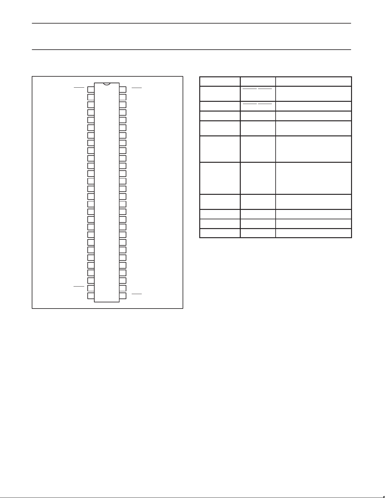
PIN CONFIGURATION
1
OEAB
2
LEAB
3
A0
4
GND
A1
5
A2
6
7
V
CC
8
A3
9
A4
10
A5
11
GND
12
A6
13
A7
14
A8
15
A9
16
A10
17
A11
18
GND GND
19
A12
20
A13
21
A14
22
V
CC
23
A15
24
A16
25
GND
A17
26
27
OEBA
28 29
LEBA
SW00485
56
CEAB
CPAB
55
B0
54
53
GND
B1
52
B2
51
NC
50
B3
49
B4
48
B5
47
46
GND
B6
45
B7
44
B8
43
B9
42
B10
41
B11
40
39
B12
38
B13
37
B14
36
35
V
REF
B15
34
B16
33
32
GND
B17
31
CPBA
30
CEBA
GTL16612
PIN DESCRIPTION
PIN NUMBER SYMBOL NAME AND FUNCTION
1, 27 OEAB/OEBA A-to-B/ B-to-A Output enable
29, 56 CEBA/CEAB B-to-A/A-to-B clock enable
2, 28 LEAB/LEBA A-to-B/B-to-A Latch enable input
55,30 CPAB/CPBA A-to-B/B-to-A Clock input
3, 5, 6, 8, 9, 10,
12, 13, 14, 15,
16, 17, 19, 20,
A0-A17 Data inputs/outputs (A side)
21, 23, 24, 26
54, 52, 51, 49,
48, 47, 45, 44,
43, 42, 41, 40,
B0-B17 Data inputs/outputs (B side)
38, 37, 36, 34,
33, 31
4, 11, 18, 25,
GND Ground (0 V)
32, 39, 46, 53
7, 22 V
35 V
CC
REF
50 NC No connection
input (active Low)
(active rising edge)
Positive supply voltage
GTL reference voltage
1999 Sep 13
3

Philips Semiconductors Product specification
18-bit GTL/GTL+ to LVTTL/TTL bidirectional
latched translator (3-State)
LOGIC SYMBOL (Positive Logic)
1
OEAB
56
CEAB
55
CPAB
2
LEAB
28
LEBA
30
CPBA
29
CEBA
27
OEBA
3
A0
CE
1D
C1
CLK
CE
1D
C1
CLK
GTL16612
54
B0
To 17 other channels
SW00254
FUNCTION TABLE
INPUTS
CEAB1OEAB1LEAB1CPAB
1
X H X X X Z
X L H X L L
X L H X H H
H L L X X B
H L L X X B
L L L ↑ L L
L L L ↑ H H
L L L H X B
L L L L X B
X = Don’t care
H = High voltage level
L = Low voltage level
↑ = Low to High
Z = High impedance “off” state
1. A-to-B data flow is shown: B-to-A flow is similar but uses OEBA
2. Output level before the indicated steady-state input conditions were established.
3. Output level before the indicated steady-state input conditions were established, provided that CP AB was Low before LEAB went Low.
OUTPUT
A
B
2
O
2
O
2
O
3
O
, LEBA, CPBA, and CEBA.
1999 Sep 13
4
 Loading...