

Philips GM 5605 User Manual

PHILIPS
MANUAL
Cathode
66-(02
58.2-10
1/86-4/01
ray
GM
oscilloscope
5605
Contents
GENERAL
I.
Introduction
II.
Technical
III.
Accessories
7
data
8
10
DIRECTIONS
I.
Installation
A.
Adjusting
B.
Earthing
C.
Checking
D.
Switching
II.
Operation
A.
Preliminary setting
B.
Displaying waveforms
FOR USE AND
C. How to use
III. Applications
A.
Measuring
B.
Using
C.
Displaying a diode
D.
Displaying a hysteresis
the X
APPLICATIONS
to the
12
before
on 13
•v,v*$r
%
the
local voltage
switching
14
the X input
-j-
•
*••
T.
amplitude
input
18
characteristic
11
on 12
15
16
18
21
loop
21
SERVICE
I.
Circuit description
DATA
A. Y
amplifier
B.
Trigger
C.
Time base
D. X
amplifier
E.
Cathode
F.
Supply
pulse
ray
part
23
shaper
generator
tube
25
-3-|
II.
Gaining
A.
Removing
B.
Removing
C.
Removing
D.
Removing
III. Maintenance
A.
Wafer switches
B.
Cabinet
IV.
Adjusting elements
access
panels
Contents
to the
the
the
the
the
parts
cabinet
knobs
front
window
36
36
and
panels
34
panel
and the
their functions
33
34
graticule
37
34
3
V.
Checking
A.
Mains current
B.
Supply
C.
Ripple
D.
Barrel
E.
Focusing
F. Y
G. X
H.
Time
VI.
Replacing
A.
Thermal fuse
B.
Supply transformer
C.
Switches
D.
Switch wafers
E.
Switch
F.
Switch
G.
Potentiometers
H. CRT and
and
adjusting
voltage
on the
and
and
amplifier
amplifier
base
generator
parts
SK2,
wafers
wafers
valves
38
+ 280 V 38
supply voltage + 280 V 38
pincushion distortion
astigmatism
39
41
45
47
47
SK3
and
SK2
48
SK3
48
SK4
48
on the
48
39
SK4
front
38
47
panel
. 48
VII.
VIII.
Fault
List
A.
List
B.
List
finding 54
of
parts
of
mechanical parts
of
electrical parts
55
58
List
of
figures
1
Adjusting
to the
local
mains
voltage
1
1
2 The
3
Preliminary setting
4
Functions
5
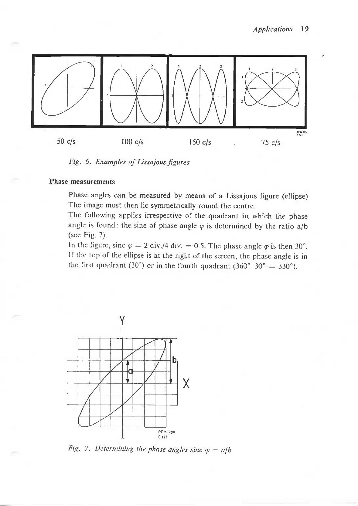
Measuring
6
Examples
7
Determining
8
Network
9
Some particular phase angles
10
Displaying
11
Displaying a hysteresis loop
12
Block diagram
13
Circuit diagram
14
Removing
15
Removing
apparatus
of the
the
of
Lissajous
the
for
quadrant
the
the
the
ia
tilted
controls
amplitude
phase angles sine
diode characteristic
of the
of the
cabinet panels
knobs
position
figures
determination
"bootstrap"
"bootstrap"
and
sockets
9? = a/b
of the OA 85
integrator
integrator
12
14
17
18
19
19
20
20
21
26
27
16
Removing
17
Removing
18
Square wave response
19
Square wave response
20
Replacing
21
Replacing
22
Anode connection
23
Positioning
24
Right-hand
25
Left-hand side view with
26
Front
27
Block diagram
28
Unit
the
the
view
A; Y
bottom plate
the
graticule
thermal
the
supply transformer
the
c.r.t.
side
view
with
adjusting elements
amplifier
and
of the Y
of the X
fuse
with
adjusting
adjusting
front panel
amplifier
amplifier
elements
elements
and
and
units
units
34
35
40
43
47
47
49
49
50
50
65
29
Circuit
30
Unit
31
Circuit
32
UnitC; X amplifier
33
Circuit diagram
34
Unit
35
Circuit diagram
36
Unit
37
Unit
38
Circuit diagram
diagram
D;
time
diagram
B;
beam
E;
H.T. unit
F;
supply
base
List
of figures 5
of the Y
generator
of the
amplifier
and
trigger
trigger pulse
67
pulse
shaper
shaper
73
79
of the X
control
of the
amplifier
81
85
c.r.t.
circuit
87
91
part
92
of the
supply
part
95
71
Important!
In
correspondence concerning this apparatus
and
serial number
as
given
on the
plate
please
at the
back
quote
of the
the
type number
apparatus.
GENERAL
PART
Introduction
The
tion
educational purposes.
amplifiers
is,
therefore, extremely suitable
two
quantities,
can be
time-base generator.
I
cathode
and is
ray
oscilloscope
particularly suitable
For X and Y
having
displayed
the
e.g.
frequency
as a
same properties
CM
and
function
5605
has an
for use in
deflection
(X-Y
for
displaying
phase relationships.
of
time
by
extensive
service
the
oscilloscope).
means
field of
workshops
apparatus
The GM
the
relationship between
Moreover,
of the
and for
contains
incorporated
applica-
d.c.
5605
voltages
8
Technical
Cathode-ray
data
Properties
stated
Numerical
instrument
tube circuit
expressed
are
guaranteed
values
and are
Tube
a.
type
b.
effective
c.
total accelerating voltage
screen area
Graticule
V
amplifier
Type
Deflection
sensitivity
Frequency response
Overshoot
Sweep expansion
Input
a.
input sockets
b.
input resistance
c.
input capacitance
d.
maximum
voltage
permissible
at
d.c.
input
without
input
in
numerical
at
nominal
tolerances
only
given
DH7-78
for the
flat
supplied)
6 x 5 cm
1750V
10 X 8div.
d.c.
amplifier
adjustable
0.1-0.3-1-3-10-30
Tolerance:
Between
ously adjusted
0-200
the
1
3 X the
and
At
can be
vertical
4-mm
500
45
kc/s
bandwidth
% for
pulses with
useful
downwards from
maximum expansion
displayed
shift
plug sockets
kO
pF in
switch
25
pF in the
55
pF in the
400
Vr.m.s.
values
mains
for
which a tolerance
voltages
indicate
the
information
on the
properties
of the
screen (other screen types
(width X height)
(1
div.
= 5.5 mm)
to 8
calibrated values:
V/div.
±3%
the
steps,
(— 3
the
sensitivity
in a
ratio
of
dB).
is: 5
Via the
c/s-200
a rise
time
screen height,
the
centre.
the
undistorted
1:
3.5
kc/s.
of ^ 25 ns
i.e.
peaks
by
control.
position
"0.01
positions
V/div."
"0.03"
and
other positions.
II
has
been
voltage adapter.
of the
user.
can be
(uncalibrated).
capacitor
1.5 X
of the
means
of the
"0.1
average
can be
0.01-0.03-
continu-
input
upwards
signal
of the
attenuator
V/div."
Technical
data
9
e.
Maximum permissible
voltage
f.
RC
X
amplifier
at the
time
of the
a.c.
capacitor input
Type
Deflection sensitivity
Response
curve
Overshoot
Sweep expansion
Input
a.
input sockets
b.
input resistance
c.
input
d.
maximum permissible
e.
Maximum permissible
f-
RC
capacitance
voltage
on
d.c, voltage
time
of the
d.c.
input
on the
capacitor input
d.c.
input
input
a.c.
input
300V
50
ms
d.c.
amplifier
adjustable
0.3-1-3-10-30
Tolerance:
Between
ously
0-200
the
bandwidth
1
% for
3 x the
left
and to the
At
maximum expansion
can be
horizontal
4-mm
500
kH
45
pF in
to 7
calibrated values:
V/div.
±3%
the
steps,
adjusted
kc/s
in a
(— 3 dB).
is: 5
pulses with a rise time ^ 25 ns.
useful
screen width,
right
displayed undistorted
shift
control.
plug
sockets
position
"0.03
switch
25
pF in the
55
pF in the
400
Vr.m.s.
position
other
300V
50 ms
the
sensitivity
ratio
of
1:
Via the
c/s-200
from
the
the
V/div"
"0.1
V/div."
positions.
0.03-0.1-
can be
3.5
(uncalibrated).
capacitor
kc/s.
i.e.
1.5 x to the
centre.
peaks
by
of the
means
of the
continu-
input
signal
of the
attenuator
Phase
Phase
Time
difference
difference
base
generator
Sweep times
Mode
of
operation
of the
amplifiers
^
5° for
that
the two
adjusted
to " x I".
adjustable
ms/div.
at a
triggered
frequencies
of
0-200
kc/s,
continuous attenuator controls
in 12
steps
from
time base length
20
fxs/div.
of 10
divisions,
provided
are
to 100
10
Accessories
Triggering
a.
required picture
ternal triggering
b.
required voltage
triggering
c.
input impedance
"EXT.TRIGG."
Supply
Mains
Influence
ations
internal
voltage
of
mains-voltage vari-
of ± 10%
height
for
external
of
socket
for in- 0.5
0.5
The
view
1
MO//20
voltage adapter
and 245 V. The
40-100
nominal
SOW.
The Y and X
inversely
or
external
division
Vp-p
maximum
of
for
for
frequencies
crosstalk).
pF
c/s
(mains frequencies
mains
proportional
frequencies
voltage amounts
for
110-125-145-200-220
mains frequency
voltage).
deflection sensitivity changes
to the
of 5
c/s-200 kc/s.
of 5
c/s-200 kc/s.
to 10
may
< 50 c/s
Power consumption
mains voltage.
Vp_p
range
only
from
(in
at
is
Mechanical
Dimensions
Weight
data
Accessories
height
width
depth
10kg
25 cm
16 cm
35 cm
v
III
1
mains
1
manual
2
test
flex
cables

11
DIRECTIONS
AND
Installation
A.
ADJUSTING
APPLICATIONS
I
TO THE
The
apparatus
200-220
The
panel.
-
Remove
-
Pull
uppermost
-
Refit
and 245 V by
adjusted value
The
instrument
the
the
adapter
the
cover
FOR USE
LOCAL
can be
cover
and
plate.
can be
out a
then
adjusted
means
is
adjusted
plate
little, turn
press
MAINS
read through
at the
VOLTAGE
to
mains voltages
of a
voltage
to
another mains voltage
rear
it
the
adapter back again.
the
(Fig.
until
adapter.
1).
round
the
correct
of
110-125-145-
opening
in the
as
voltage
rear
follows.
value
is
j
-
.
.
.
-
V
Fig. L Adjusting
voltage
to the
local
mains
12
Installation
B.
EARTHING
Earth
the
instrument
may
be
done
- via the
a
plug with rim-earthing
-
via one of the
mains
flex,
earthing
in
accordance
if
the
apparatus
contacts,
sockets
with
has a
or
("•=•")
the
local
3-core
at the
safety
mains
front
regulations.
flex
provided
of the
apparatus.
This
with
Double
C
CHECKING BEFORE SWITCHING
-
Check
-
Check whether
- Set
-
Connect
earthing connections
the
knob
setting
"INTENSE
the
of the
the
apparatus
apparatus
may
cause
hum and
must
be
ON
mains voltage adapter (see section
has
been properly earthed (see
to
position
to the
"0".
mains
via the
mains
flex.
avoided.
A).
section
B).
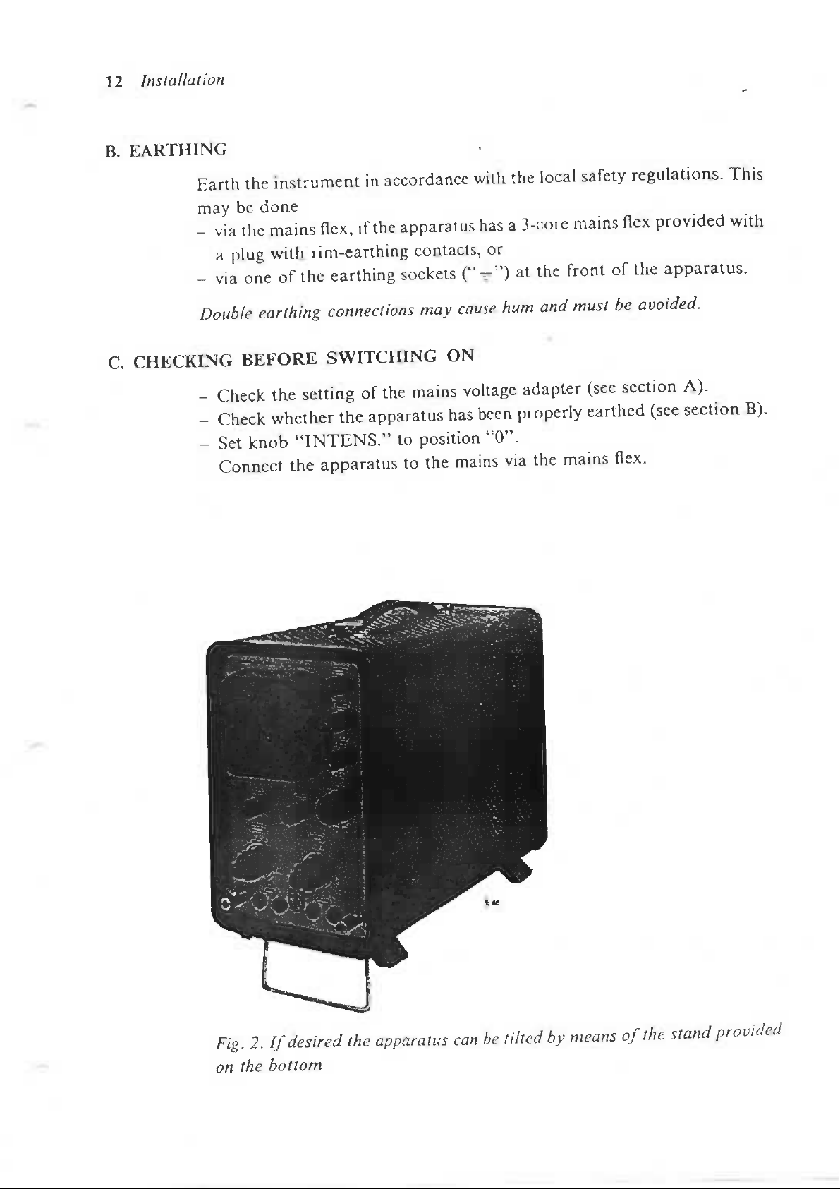
Fig.
on
the
2.
If
bottom
desired
the
apparatus
can be
tilted
by
means
of the
stand provided

D.
SWITCHING
ON
Installation
13
Switch
to
A
a
on the
apparatus
approximately
stationary picture
time
may
permanently damage
by
setting
its
central position.
of
maximum
knob
brightness,
the
screen.
"INTENS."
left
on the
from position
screen
for too
"0"
long

14
Operation
A.
PRELIMINARY SETTING
- Set
all
knobs
-
Adjust
knobs
-
Check
If
VI.H.l.
-
Adjust
controls
the
time
"jYf
whether
necessary,
the
definition
"FOCUS."
to the
and
positions
base
"<-X-»".
the
time
line
reposition
and the
and
indicated
to the
base line
the
centre
appears horizontally
picture
brightness
"INTENS.".
in
of the
tube
of the
Fig.
3.
screen
in
accordance
picture
by
by
means
on the
with
means
II
of the
screen.
section
of the
Fig.
3.
Preliminary
17*.
setting

Notes
- If the
and
on the
base
that
turned (see
-
If
of the X
must
longer
the
time
"|Yj",
left-hand
line
the
knob
be
shifts
With cathode
screen
meter
"ASTIGM.",
base
line
cannot
potentiometer
side
of the
appears.
picture
section
"X
AMPL."
amplifier (accessible
adjusted
if the
is not
This
potentiometer must
does
not
shift
V.F.I).
is in
in
such a way, that
continuous control
ray
tubes,
round.
astigmatism
This
accessible
be
displayed
"DC-Balance"
apparatus) must
if the
position
on the
can be
continuous
"0.3
right-hand side
on the
V/div.",
the
is
may
corrected
left-hand side
Operation
by
means
of the Y
be
be
light
turned (see section V.G.
arise.
of
knobs
amplifier
turned until
adjusted
control
knob
spot
Then
by
in
"Y
"DC-Balance"
of the
on the
the
means
of the
"<—X-V*
(accessible
the
such a way,
AMPL."
apparatus)
screen
light
spot
of
potentio-
apparatus.
15
time
is
no
I).
on
B.
DISPLAYING
1.
Time
Note;
meter
according
2.
Time
WAVEFORMS
base
internally
-
Adjust
Turn knob
appears.
-
Apply a voltage
Turn
-
Place
base
-
Adjust
Turn knob
appears.
-
Apply a voltage
-
Apply
right-hand
voltage
originates).
-
Place
as
described under "Preliminary
"STAB.*'
knob
If no
"LEVEL"
externally
"STAB."
knobs
knobs
"Y
triggering
to
section
as
described under "Preliminary
"STAB."
an
external trigger voltage
side
must
"Y
triggered
anti-clockwise,
to the
until a stable
AMPL."
occurs
(R513,
V.H.I.
triggered
anti-clockwise
to the
of the
be
derived from
AMPL."
apparatus
until
d.c.
or
a.c. input
picture
and
"NV*
at
in the right-hand
d.c.
or
the
and
in the
minimum
until
a.c. input
to
socket
(if the
voltage from which
"N\
picture must
at the
setting"
the
of the Y
is
required
setting
side wall) must
setting"
the
of the Y
required
(page 14).
time base
amplifier.
obtained.
position.
(0.5 div.),
(page 14).
time base
amplifier.
"EXT.TRIGG."
be
the Y
position.
line
just
dis-
potentio-
be
adjusted
line
just dis-
on the
stationary, this
signal
also
16
Operation
C. HOW TO USE THE X
If a voltage
with
each other
Some
of
-
Connect
AMPL."
-
Place switches
-
Set the
The
picture
trols
"jYf"
In
order
amplifier
is
applied
and
these applications
the
voltages
and "DC
continuous control
can now be
and
to
obtain good stationary pictures,
inputs should
INPUT
to
both
amplifiers,
their
relationships
are
to be
compared
(AC) X AMPL.".
"Y
AMPL."
"X
brought
"<-X-»-".
be
synchronous.
these voltages
can be
also mentioned
to the
and
"X
AMPL."
AMPL"
on the
to
screen
position " X 1".
made
input
visible.
in
chapter III.
sockets
in the
by
means
the
voltages
can be
compared
"DC
(AC)
Y
desired position.
of the
shift
con-
on the two
•
Step
.-Iit* W Uw
Horl(««l
VcrUcil
vertici
picture
(Hcun
(ta
dull
BnC|.U>eu
I
it.-rniil
tnuii-rmj;
,-iu
,
-X
Operation
cu»n>J/ii«IH.uic
W
iKc-
pKI-re
trtf—l-r
nmul
wKk
»•
nli-nul
k
,J
|Kr
i.,
AWI'l. " ..
IH
•«
nnr
p.rt,u—
*Imi
hr
.---I
l-fc.
->H-J
11
«
lui
.
•rffUtUTWHt
••'.
|.
1<K>U*
k..i
ii.wlal
..
1..I..
il,
l
i,n,
HI
u(
«w
JKHLlHJA
(in
;;.
iv i ii
twntonul
,i
,4
UK1
I..MLH.I.
II
IWllClKd
Cxndnuuui
>elt«lUVt1l'
1>V('
IH>)
ih.
li....
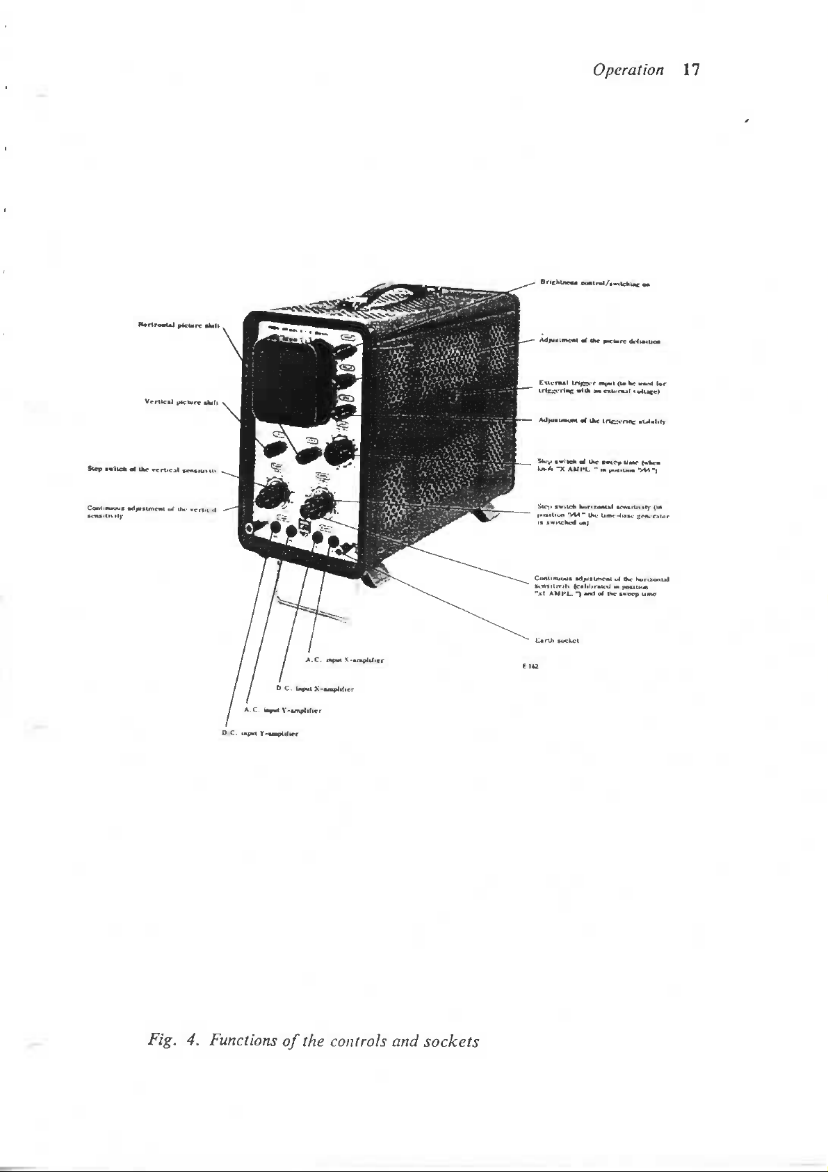
Fig.
4.
Functions
of the
controls
and
sockets
18
Applications
A.
MEASURING
-
Measure
-
Determine
(continuous
Now
height)
THE
the
the
amplitude
= 30 V.
\.
AMPLITUDE
distance
the
position
attenuator
between
of
in
amounts
the
peaks,
knob
"Y
AMI*!./1
position " x
to 10
(attenu;,i0r
c.j/. 3 div. (see Fig.
l"j,
e.g.
10
V/div.
position)
x3
III
5)
(picture
B.
USING
THE X
The
Frequency
Phase measurements
Displaying characteristics
Etc.
Frequency
If a
spot
influence
Dependent
peaks.
INPUT
following examples
measurements
measurement
voltage
on the
of
screen
of a
on the
The
unknown
number
number
by
unknown
will
voltage
frequency
of
peaks
of
peaks
means
frequency
PEM
217
EI:S
can be
frequency
mentioned:
of
Lissajous
is
applied
describe a so-called
of
known frequency applied
the
image
K-
figures
Lissajous
will
at the top
X
at the
side
known frequency.
5.
Measuring
to the Y
the
amplifier,
figure,
to the X
show a certain
amplitude
the
light
under
the
amplifier.
number
of
Some
used
common
as
reference
Lissajous
frequency.
figures are
shown
in
Fig.
6, in
which
50 c/s is
Applications
19
50c/s
Fig.
Phase
measurements
Phase
The
The
angle
(see
In the figure,
If
the top of the
the
100
6.
Examples
angles
of
can be
image must then
following
is
found:
Fig.
applies irrespective
the
7).
sine
<p
ellipse
first
quadrant
(30°)
c/s
Lissajous
figures
measured
lie
symmetrically round
sine
of
phase angle
— 2
div./4 div. — 0.5.
is at the
or in the
by
right
fourth
150c/s
means
of the
<p
of the
quadrant
of a
Lissajous
the
centre.
quadrant
is
determined
The
phase angle
screen,
75
c/s
figure
in
which
by the
the
phase angle
the
<p
is
(ellipse)
phase
ratio
then
a/b
30°.
is in
(360°-30° = 330°).
Fig.
7.
Determining
the
P£M
E12J
phase
290
angles
sine
<p
= a/b
20
Applications
If the top is at the
(180°-30° - 150°)
determination
-
Include a circuit
closed
-
Open
mum
Fig.
switch.
the
value.
8.
Network
of the
switch
In
for
left
of the
or in the
quadrant
as
shown
and
turn
doing
so, the
quadrant
screen,
third
proceed
in
the
shape
determination
the
quadrant (180
as
Fig. 8 into
potentiometer
of the
PEM
289
E127
angle
follows:
the
lead
ellipse
is in the
+ 30° =
to the X
from
minimum
must
second quadrant
210°).
amplifier
clearly
For
with
to
maxi-
change.
Phase
angle (thus also
becomes
larger
smaller
If
the
picture appears
angle
is 0°
y=0°(360°)
(360°)
a)
as a
or
180° (Fig.
Quadrant
2.
(90°-I80°)
3.
(180°-270°)
straight
diagonal
9).
¥>
=90°(270°)
on the
PEM2M
Quadrant
1.
(0°-90°)
4.
(270°-360°)
screen,
the
phase
Fig.
9.
Some
particular
phase
angles
C.
DISPLAYING A DIODE CHARACTERISTIC
In
displaying a diode characteristic
plotted
made
sinewave voltage.
expected internal resistance
directly proportional
anode
which
voltage.
as a
function
of the
voltage
represents
circuit shown
is
of the
The
to the
applied
the
voltage
in
Fig.
resistance R must
of the
anode current,
to the X
relationship between
10.
diode.
the
current
across
amplifier.
the
Voltage
be
The
is fed to the Y
anode
Applications
through
diode.
source E supplies
small with respect
voltage
Now a
For
curve
current
the
this,
across
amplifier.
diode
use can be
R,
is
displayed
and
21
a low
to the
which
The
anode
is
is
Fig.
10.
Displaying
D.
DISPLAYING A HYSTERESIS
In
displaying
B
is
plotted
contains
through
of the field
mary
winding.
hysteresis
as a
no air
the
number
strength
the
function
gaps,
The
(see Fig. 12).
The
voltage
Here
k is a
This
voltage
across
proportional
low and
across
constant.
is
the
capacitor then becomes
to the
must
the
integrated
be
adequately amplified,
diode characteristic
LOOP
loops
the field
of
H. A
voltage
voltage
of
magnetic
of the field
strength
windings.
resistor
across
secondary winding
by an RC
across
The
Rp is
Uc = k.B/R.C.
of the OA 85
material,
strength
is
primary
connected
this
resistor
is Us = k.dB/dt.
network
the
capacitor.
is fed to the Y
the
magnetic
H.
If the
proportional
current
is
(R»
iron
is
in
series
applied
I/o>c).
The
induction
This
voltage,
amplifier.
induction
core
of a
coil
to the
thus a measure
to the X
with
The
current
the
pri-
input
voltage
B is
thus
which
is
22
Applications
Fig.
11.
Displaying a hysteresis loop
Note - It is
to the Y
the
axis.
screen
possible that
The
peak
by
reversing
the
trace
of the
the
connections
is
displayed
hysteresis
of one of the
as a
loop
mirror i mage
is
brought
to the
coil
windings.
with
right
respect
of
23
SERVICE
Circuit
A. Y AMPLIFIER
diagram
The
The
(AC)
circuit
1.
Attenuator circuit
An
the
In
ed is
A
in
positions.
C30,
in
DATA
amplifier
voltage under test
and
attenuator circuit, which
input
the
positions
attenuated
step attenuator with high impedance
the
other positions
C31,
all
positions
I
(unit
and a
A,
Fig.
29)
for the Y
subsequently applied
phase inverter.
circuit
By
C32 and
of the Y
"3
V/div."
by the
means
of SK3 the
deflection
is
connected
is
amplifier.
and
voltage dividers
of
SK3.
of the
C33,
trimmers C27,
the
attenuators
attenuation
is a
d.c.
to
socket
to the
operated
"10
The
output
by
V/div."
R34-R26//R41
(R36-R28
attenuator switch
C28 and C29 and the
are
is
frequency independent.
coupled
means
of
push-pull
BU2
(DC)
amplifier
SK3, thesignal
adjusted
of
...
or to
via an
SK3,
and
R32)
has
in
amplifier.
socket
attenuator
is
included
to be
R35-R27//R41
is
eight calibrated
such
a way
BU3
in
measur-
included
capacitors
that
2.
Phase
inverter
Via
the
phase
control grid
cathode resistor R40.
R42, this valve
signal
the
anodes
voltage
The
amplitude
value
by
means
Turning
d.c. voltage
stage
attenuator
inverter
to be
difference
of the
stage
of
valve
is
measured,
of
Bl
of the
anode resistors
of
potentiometer
potentiometer
on the
circuit
with
driven
and B2 are
between these
input
the
Bl.
Valves
As the
by a
but
signal
R6
of the
the
signal
valves
control grid
voltage whose magnitude
opposed
symmetrical with
can be
R43 and R49 - and
R6.
would also result
next
to be
Bl
and B2.
Bl and B2 are
in
phase
anodes.
adjusted continuously
amplifier
measured
This
of B2 is
to the
respect
in a
stage
is
stage
coupled
connected
latter.
to the
thus
variation
(B1
'-B2'),
applied
is
driven
via the
to
is
equal
The
voltage
average d.c.
by
varying
the
amplification
of the
which would
to the
on the
common
earth
via
to the
on
the
average
-
24
Circuit
description
3.
Output
give
rise
to a
equalizing
by
means
arises
across
Resistor
current
resistor
C34.
R37 in the
in the
on the
stage
shift
of the
the
values
of
potentiometer
of the
R6.
control
case
of
positive
square
light
wave
spot
on the
d.c. voltages
R57
(DC-Balance),
grid
circuit
input
response
signals.
is
screen. This
on the
of
valve
The
eliminated
anodes
so
that
Bl
serves
adverse
by
is
avoided
of
Bl'
and
no
d.c. voltage
to
limit
influence
the
of
by
B2'
grid
this
parallel capacitor
Output
B2',
citance
B2.
Bl
shift
cathode
the
of
shift
to the
impedance
voltage
dependent
balance
dividers
meter
that
The
common
nected
the
age of B3,
shaper
amplifier
which
As a
are
of the
result
output
and B3 or B2 and
controls
R4-R4'
followers.
control grids
Bl'
opposite
in the
vertical
control grids
R76-R64
dividers
of the
is
maintained. Capacitors
from
affecting
R80 the
the
maximum Y sensitivity
symmetry
cathode
to the Y
case
of
internal
which
via
switch SK5.
B3-B3'
provided
is
to
valves
the
bandwidth
B3'
were
are
By
means
of
Bl'
and
to
that
on the
direction
of
Bl'
and
the
anode potentials
position
the
feedback
of the
of
signal
resistor.
deflection
triggering
is
applied
preceded
reduce
on the
of the
by the
the
influence
anode impedance
amplifier
directly coupled
included
of
B2'
across
and
R72-R70
of the
in the
these potentiometers
can be
grid
B2'
of
the
screen.
via the
varied.
B2'.
respectively.
of
valves
shift
controls
C36 and C37
square wave
response.
both output valves
is 10
in the
The
anodes
plates.
use is
to the first
mVp-p/div.
output stage
of B3 and
For
driving
made
of
valve (B501)
cathode
of the
is
larger than
to the
control
The
As a
The
result
shift
voltage
Bl
and B2 are
(R4,
By
is
adjusted
is
B3'
the
time
that part
followers
high
of the
Bl'
input
valves
Bl and
if the
preceding stage.
grid
circuit
the
d.c.
variation
the
voltage
dividers
By
means
of the
voltage
on the
image
is
applied
with
of
made
R4'),
prevent
increased
so
means
in
are
that
the
the
voltage
of
potentio-
such
due to the
directly con-
base generator
of the
of the
anode volt-
trigger pulse
and
capa-
valves
The
on
grid
will
high
these
in-
d.c.
a way
in
B.
TRIGGER PULSE
The
trigger pulse shaper consists
Schmitt
The
trigger
well
as
SHAPER
trigger
signal,
from
an
(unit
D,
(B502-B502').
which
external
may
voltage
Fig.
31)
of an
originate
source,
amplifier
from
the Y
is
applied
stage (B501)
amplifier
to the
control
and a
(R85)
grid
as
of
 Loading...