

Philips FXA1012WC Datasheet

IMAGE SENSORS
FXA 1012
Frame Transf er CCD Image Sensor
Objective specification 2000 January 7
File under Image Sensors
Philips
Semiconductors

Philips Semiconductors Objective specification
g
Frame Transfer CCD Image Sensor FXA 1012
• 2M active pixels (1616H x 1296V)
• 2/3-inch type optical format
• Still and monitor modes
• RGB Bayer pattern colour filter s
• Progressive scan
• Excellent anti-blooming (V ertical Overflow
Drain)
• High dynamic range (>70dB)
• High sensitivity
• Low dark current and low fixed pattern noise
• Low read-out noise
• V ariable electr onic shuttering
• Data rate up to 25 MHz, 5 frames/s
• Small outline LCC package
• Low cost
Device structure
Optical size: 8.16 mm (H) x 6.53 mm (V)
Chip size: 9.49 mm (H) x 9.32 mm (V)
Pixel size: 5.1 µm x 5.1 µm
Active pixels: 1616 (H) x 1296 (V)
Total no. of pixels: 1688 (H) x 1324 (V)
Optical black pixels: Left: 2 Right: 70
Optical black lines: Top: 12 Bottom: 12
Total no. of storage lines: 298
Dummy register cells: 8
Description
The FXA 1012 is a colour frame-transfer CCD image sensor designed
for consumer digital photography applications. The combination of
high speed and a high linear dynamic range of over 10 true bits
makes this device the perf ect solution for use in compact high quality
imaging applications. Two modes of operation provide both a
monitoring image for LCD screens, and a full resolution, zero-smear
still image with excellent colour rendition. The device structure is
shown in figure 1.
12 dark lines
8 black lines
Image
Section
1616 active pixels
12 dark + 4 dummy lines
Storage Section
298 lines x 1688 cells
1688 cells
Output re
ister
GBGB
RGRG
GBGB
1296
active
lines
GBGB
RGRG
70
Output
amplifier
8
GBGB
RGRG
GBGB
2
GBGB
RGRG
Figure 1 - Device structure
2000 January 2

Philips Semiconductors Objective specification
Frame Transfer CCD Image Sensor FXA 1012
Architecture of the FXA 1012
The FXA 1012 consists of an open image section and a storage
section with an optical light shield. An output register and amplifier
are located below the storage section for read-out.
The optical centres of all pixels in the image section form a square
grid. The image area has RGB Bay er colour filter pattern. The charge
is generated and integrated in the image section. This section is
controlled by four image cloc k phases (A1 to A4). After the integration
time the image charge is shifted one line at a time to the storage
section.
The storage section is controlled by four storage clock phases (B1
to B4). In the still mode the image inf ormation is transported straight
IMAGE SECTION
Image diagonal (active video only)
Aspect ratio
Active image width x height
Pixel width x height
Image clock pins
Capacity of each clock phase
Number of active lines
Number of black reference lines
Number of dummy lines
Total number of lines
Number of active pixels per line
Number of black reference pixels per line
Total number of pixels per line
10.4 mm
5:4
8.24 x 6.61 mm
5.1 x 5.1 µm
A1, A2, A3, A4
5.4 nF per pin
1296
24 (12+12)
4
1324
1616
72 (2+70)
1688
through the storage section to the horizontal output register. In the
monitoring mode subsampling of the image is performed at the
image-to-storage transition and the subsampled image is stored in
the storage section. The stored image is shifted one line at a time
into the horizontal output register.
In the next active line time the pixels are transpor ted towards the
output amplifier. Four clock phases (C1 to C4) control the pixel
transport in the output register. In the output amplifier the charge
packets are dumped one by one on a floating diffusion area. The
voltage of this area is sensed and buffered by a three-stage FET
source-follower. Figure 2 shows the detailed internal structure.
2
2
STORAGE SECTION
Cell width x height
Storage clock pins
Capacity of each clock phase
Number of cells per line x number of lines
5.1 x 5.1 µm
B1, B2, B3, B4
1.5 nF per pin
1688 x 298
2
OUTPUT REGISTER
Number of dummy cells
Total number of register cells
Output register clock pins
Capacity of each clock phase
Reset Gate (RG) capacity
Output stage
8
1696
C1, C2, C3, C4
60 pF per pin
15 pF
3-stage source follower (open source)
2000 January 3

Philips Semiconductors Objective specification
Frame Transfer CCD Image Sensor FXA 1012
Operational modes
The FXA 1012 is designed for high-resolution digital photography
with real time monitoring at reduced resolution. T w o diff erent modes
of operation make this possible.
In the still picture mode the high-resolution image is read-out directly .
A mechanical shutter ensures a 100% smear-free image with a
resolution of 1600 (H) x 1280 (V).
A1
A2
A3
A4
12 lines
1296 active
images
lines
16 lines
OG: output gate
RG: reset gate
One Pixel
A1
A2
A3
A4
A1
A2
A3
A4
A1
A2
A3
A4
A1
A2
A3
A4
A1
A2
A3
A4
B1
B2
B3
B4
RD: reset drain
B1
B2
B3
OUT
RG
RD
OG
8 dummy pixels
B4
C4C2 C1C3C4C2 C1C3 C4C2 C1C3C4C2 C1 C4C2 C1C3 C4C2 C1C3 C4C2 C1C3 C4C2 C1C3 C4C2 C1C3 C4C2 C1C3
column
1
2 black timing
columns
298 storage
lines
column
2+1
1616 image pixels
In the monitoring mode, images with reduced vertical resolution are
produced that are suitable for LCD displa ys. These images can hav e
for example, 120, 240 or 256 lines at up to 40 images per second.
A1
A2
A3
A4
A1
A2
A3
A4
A1
A2
A3
A4
IMAGE
FT CCD
STORAGE
column
2+1616
70 black timing columns
A1
A2
A3
A4
A1
A2
A3
A4
A1
A2
A3
A4
B1
B2
B3
B4
B1
B2
B3
B4
column
2+1616+70
A1, A2, A3, A4: clocks of image section
B1, B2, B3, B4: clocks of storage section
C1, C2, C3, C4: clocks of horizontal register
Figure 2 - Detailed internal structure
2000 January 4

Philips Semiconductors Objective specification
Frame Transfer CCD Image Sensor FXA 1012
Specifications
Absolute Maximum Ratings Min. Max. Unit
GENERAL:
storage temperature
ambient temperature during operation
voltage between any two gates
DC current through any clock phase (absolute value)
OUT current (no short circuit protections)
VOLTAGES IN RELAT ION TO VPS:
VNS, RD
all other pins
VOLTAGES IN RELAT ION TO VNS:
RD
VPS
all other pins
-40
-20
-20
-0.2
0
-0.5
-10
-10
-30
-30
+80
+60
+20
+2.0
4
+30
+25
+0.5
+0.5
+0.5
°C
°C
V
µA
mA
V
V
V
V
V
Max. current
[mA]
2
2
2
3
5.5
1
-
-
VNS
VPS
SFD
SFS
OG
RD
1
N substrate
P substrate
Source Follower Drain
Source Follower Source
Output Gate
Reset Drain
DC Conditions Min. [V] Typical [V] Max. [V]
20
6
19
0
3.5
19
24
7
20
0
4
20
28
9
21
0
4.5
21
Min. Typical Max. Pin
Number of adjustments 0 0 1 VNS
1
To set the VNS voltage for optimal Anti-Blooming (vertical overflow drain), it should be adjustable between minimum and maximum values.
2
Currents INS and IPS are specified at overexposure of 100 x Qmax.
3
Measured with Rload = 3.3 kOhms.
AC Clock Level Conditions Min. Typical Max. Unit
IMAGE CLOCKS:
A-clock amplitude
A-clock low level
11 12
0
13 V
V
STORAGE CLOCKS:
B-clock amplitude
B-clock low level
11 12
0
13 V
V
HORIZONTAL AND RESET CLOCKS:
C-clock amplitude
C-clock low level C1, C3
C-clock low level C2, C4
Reset Gate (RG) amplitude
Reset Gate (RG) high level
4.5
2.5
4.5
21
5
0
3
5
22
5.5
3.5
5.25
23
VNS PULSE:
Charge Reset (CR) pulse on VNS 4.5 5 5.5 V
2000 January 5
V
V
V
V
V
Philips Semiconductors Objective specification
Frame Transfer CCD Image Sensor FXA 1012
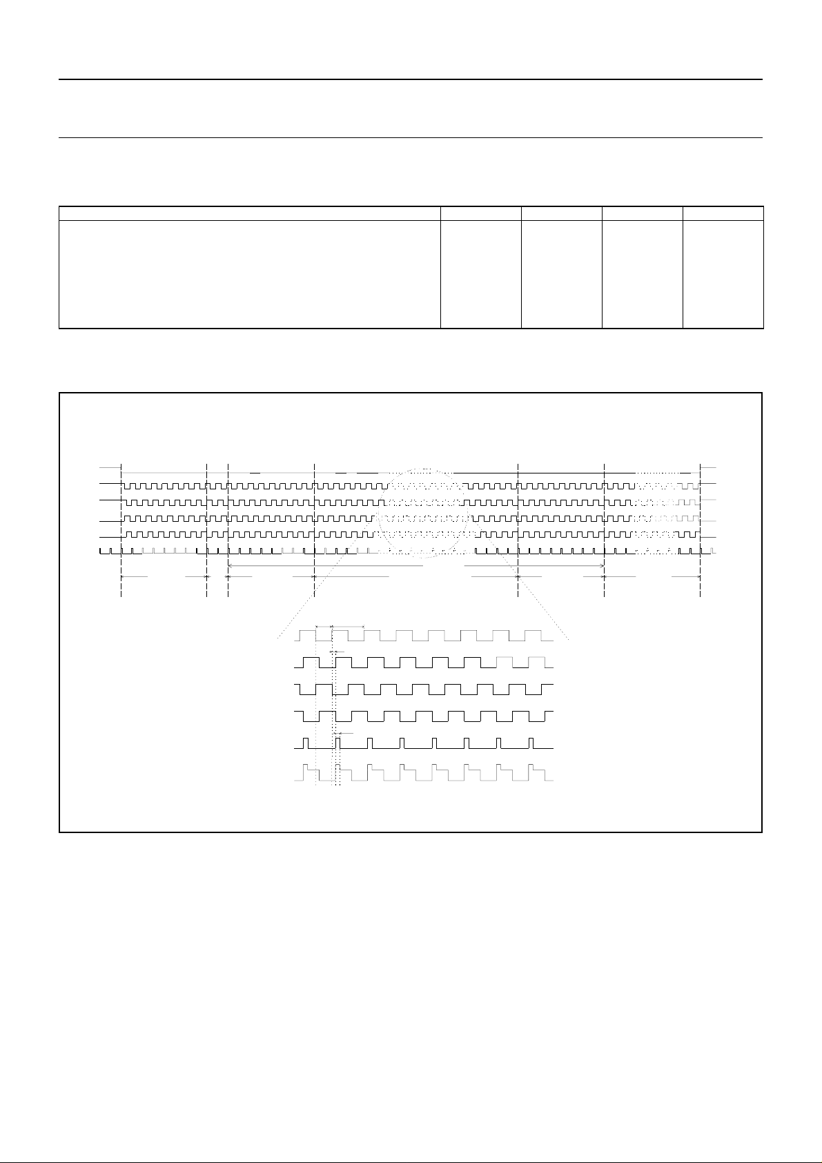
Timing diagrams (for default operation)
AC Characteristics Min. Typical Max. Unit
Horizontal frequency
Vertical frequency
Charge Reset (CR) time
Rise and fall times: image clocks (A)
register clocks (C)
reset gate (RG)
1
Typical value for monitor mode.
2
Duty cycle = 50%
3
Tp is pulse period of C clocks
C-clock pulses
FREQUENCY = 25 MHz
SSC
C1
C2
C3
C4
RG
blue (even) lines
red (odd) lines
8 dummy pixels
2
black 1600 active pixels within aspect ratio
pixels
10
2
10
3
3
COMPLETE LINE READOUT CYCLE
8 overscan pixels
RG G RGR
GBGB
RGR
C1
C2
G
GB
RG
20ns
G
R
6ns
G
B
BG BG
R
GRG
25MHz HORIZONTAL TRANSPORT PULSES
40ns
1616 active pixels
BGGBGBG G
....
..
.
..
..
.
.
.
G
1.56
12
20
5
5
GRG
8 overscan pixels
G
B
RGR
1
BGB
R
25
MHz
MHz
14
3
Tp/8
Tp/8
70 black pixels
BB
G
RG
µs
ns
ns
ns
C3
C4
RG
SENSOR SIGNAL
6.7ns
Figure 3 - Timing diagram for horizontal pulses
2000 January 6
 Loading...