

Page 1

BU TUNERS
DATA SH EET
FM1216
Desktop video & FM radio module
system B/G
Preliminary specification
File under BU Tuners, DC03
1997 Mar 13
Page 2

Philips Components Preliminary specification
Desktop video & FM radio module
system B/G
FEATURES
• System B and G, and FM radio broadcast
• True 5 V device (low power dissipation)
• Full frequency range from channel 2
(48.25 MHz) to channel 69 (855.25 MHz)
• FM radio band coverage from 87.50 MHz to
108.00 MHz
• PLL controlled tuning
• Programmable PLL step size (31.25, 50 or 62.5 kHz)
• True-synchronous vision IF demodulator (PLL)
• Ultra linear FM PLL demodulator for FM radio broadcast
• Demodulated video output, AF sound output, second
sound IF output
• I2C-bus control of tuning, address selection, AFC status
information
• Complies with European regulations on radiation, signal
handling and immunity
‘‘Amtsblatt 15/92”)
• Small horizontally mounted metal housing.
DESCRIPTION
The FM1216 front-end is designed to receive both TV and
FM stereo signals in the PC Multimedia environment. The
units are available with separate 75 Ω inputs for TV and
FM broadcast reception. The input connectors available
are either standard phono or IEC type (female for TV, male
for FM radio). The tuning, bandswitching and antenna
selection are made through the I2C-bus.
The front-end covers the TV bands from 48.25 MHz to
855.25 MHz. The FM band covers the standard
87.50 MHz to 108.00 MHz. An RDS decoder can be
connected to the AF-MPX output. The FM1216 meets the
input immunity and radiation requirements of CENELEC.
The FM1216 consists of a TV tuner, an FM radio tuner and
an IF section, all designed on a single PCB. The front-end
is assembled in a metal housing made of a rectangular
tin-plated steel frame, with front and rear covers, which
have soldered contacts to the frame. The two phono or
IEC antenna connectors (female for TV, male for FM
radio) are mounted on one side of the frame for the TV/FM
signal inputs. All other connections are made via pins at
the bottom.
(“CENELEC 55020, 55013’’
and
FM1216
In the FM radio mode, the level detector and AFT functions
are provide for the auto-search routines. The level detector
and AFT status can be read from the A/D bits in the
status-byte. The mute function is also provided to
suppress the audio output signal, if required.
The tuner AGC for both TV and FM radio operation, is
generated with a novel AGC detector which measures the
IF signal level directly at the tuner IF output pins. As
opposed to the conventional AGC detector, this new circuit
allows a higher take-over level and offers superior
immunity against tuner overload.
The demodulation of the TV sound and FM radio IF
(10.70 MHz) is done with a PLL demodulation circuit
contained in the IF IC. In the FM radio mode, the
multiplexed AF signal is then channelled to a stereo
decoder IC which extracts the left/right analog signals. The
multiplexed audio signal is also available at pin 25 to
support RDS or BTSC implementations. The 2
sound output is provided to connect external
(analog 2 carrier or digital) stereo processing.
ORDERING INFORMATION
TYPE DESCRIPTION
FM1216/HM/PH standard phono 3139 147 13371
FM1216/HM/I IEC connector 3139 147 13381
MARKING
The following items of information are printed on a sticker
that is on the top cover of the tuner:
• Type number
• Code number
• Origin letter of factory
• Change code
• Year and week code.
nd
IF TV
CATALOGUE
NUMBERS
The TV IF section uses an intercarrier SAW filter, followed
by a true-synchronous vision IF demodulator (PLL) IC. The
analog AFC voltage is fed to the 5-level A/D converter in
the PLL tuning IC, so that the AFC status can be read via
the I2C-bus.
1997 Mar 13 2
Page 3

Philips Components Preliminary specification
Desktop video & FM radio module
FM1216
system B/G
INTERMEDIATE FREQUENCIES
SYSTEM
FREQUENCY
(MHz)
Picture carrier 38.90
Colour 34.47
Sound 1 33.40
Sound 2 33.16
NICAM 33.05
FM 10.70
PINNING
SYMBOL PIN DESCRIPTION
V
T
V
S(tuner)
11 tuning voltage (monitor)
12 supply voltage tuner section +5 V
SCL 13 I
SDA 14 I
AS 15 I
AF O/P right 20 FM radio right channel
AF O/P left 21 FM radio left channel
nd
IF O/P 22 second IF TV sound output
2
CVBS 23 Composite Video Baseband Signal (CVBS) output
V
S(IF)
24 supply voltage IF section +5 V
AF O/P 25 AF sound output
− TH1, TH2, TH3 and TH4 mounting tags (ground)
CHANNEL COVERAGE
BAND
FREQUENCY
(MHz)
FM radio band 87.50 to 108.00
Low band 48.25 to 170.00
Mid band 170.00 to 450.00
High band 450.00 to 855.25
2
C-bus serial clock
2
C-bus serial data
2
C-bus address select
1997 Mar 13 3
Page 4

Philips Components Preliminary specification
Desktop video & FM radio module
system B/G
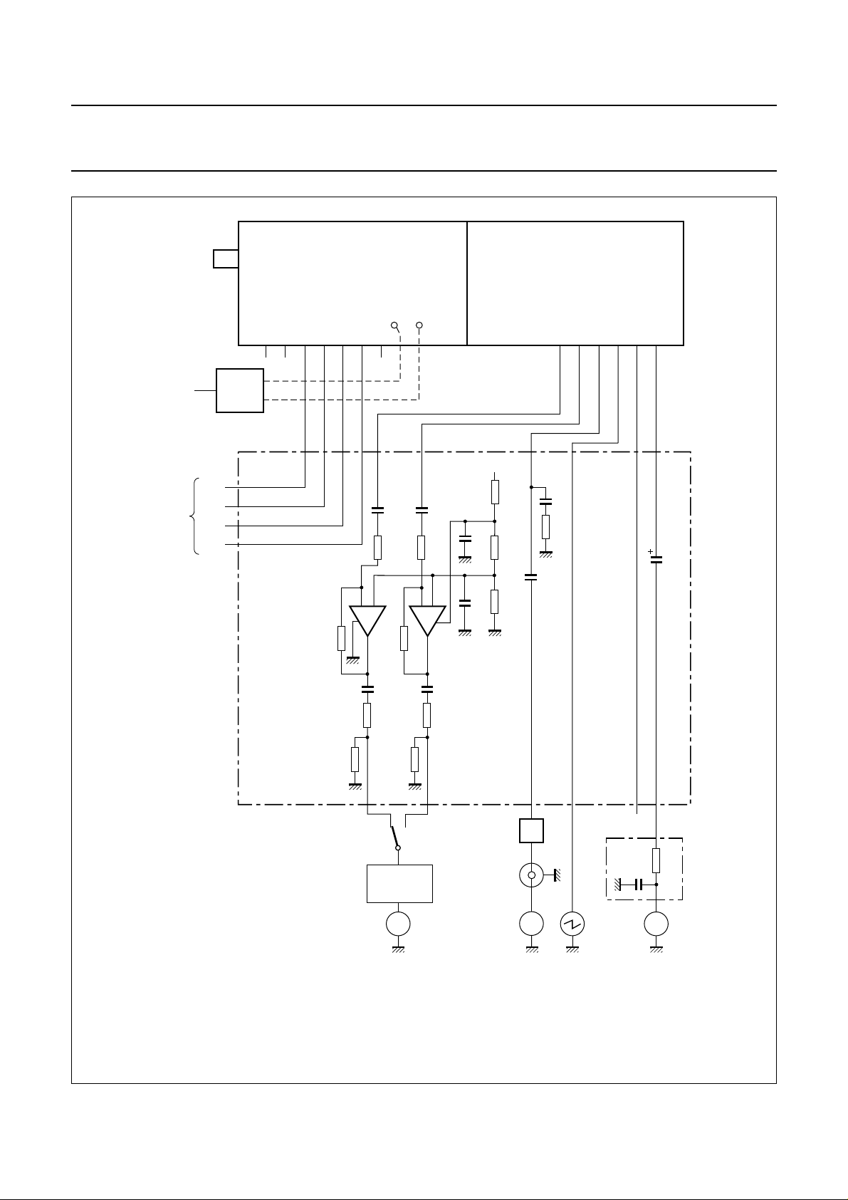
BLOCK DIAGRAM
2nd IF
FILTER
10.7 MHz
FILTER
AGC
DETECTOR
SAW
IF
V
VCO
PLL
VIF
DEMODULATOR
TRAP
FM
DEMODULATOR
FM-IF
10.7 MHz
DISCRIMINATOR
STEREO
DECODER
FILTER
10.7 MHz
FM1216
AF
(TV)
S(IF)
+5 V
V
CVBS
23
sound
output
2nd IF
AF-R AF-L
IF
MIXER - OSCILLATOR IC
HIGH BAND
OSC.
HIGH
MID
OSC.
MID BAND
LOW
OSC.
LOW BAND
VT
AFT
PLL
DC-DC
11 12 13 14 15 20 21 22 2524
CCA505
AS
SDA
SCL
+5 V
VT
S( tuner)
V
monitor
Fig.1 Electrical block diagram.
handbook, full pagewidth
TV
antenna
FM
antenna
1997 Mar 13 4
Page 5

Philips Components Preliminary specification
Desktop video & FM radio module
FM1216
system B/G
LIMITING VALUES
Limiting values under operational conditions
The tuner can be guaranteed to function properly under the following conditions.
SYMBOL PARAMETER PIN MIN. TYP. MAX. UNIT
V
S
V
S(ripple)
I
S(tuner)
V
SCL
V
SDA
I
SDA
V
AS
V
AFright(FM)
Z
AFright(FM)
V
AFleft(FM)
Z
AFleft(FM)
Z
IF
Z
CVBS
t
L
V
S(IF)
I
S(IF)
Z
AF
supply voltage
peak-to-peak ripple voltage susceptibility
(at5V±5%); note 1
20 Hz to 100 kHz −−5mV
12
>100 kHz to 500 kHz −−10 mV
supply current −−120 mA
SCL bus input voltage 13 −0.3 − +5.25 V
SDA bus input voltage
SDA bus current (open collector) −1 − +5 mA
14
address select voltage; note 2 15 −−+5.25 V
FM right channel DC voltage
FM right channel load impedance parallel connected:
resistive value − 50 − kΩ
20
capacitive value − 9 − pF
FM left channel DC voltage
FM left channel load impedance:
resistive value − 50 − kΩ
21
capacitive value − 9 − pF
2nd IF sound output load impedance 22 0.5 −−kΩ
Composite Video Baseband Signal load impedance
CVBS load time constant −−100 ns
IF supply voltage
IF supply current −−150 mA
23
24
AF sound output load impedance parallel connected:
25resistive value 5.0 −−kΩ
capacitive value −−4nF
4.75 5.00 5.25 V
−0.3 − +5.25 V
− 1.0 − V
− 1.0 − V
− 75 −Ω
4.75 5.0 5.25 V
Notes
1. Sinusoidal ripple voltage superimposed on the 5 V supply voltage in the frequency range of 20 Hz to 500 kHz.
Criteria for TV interference >57 dB.
2. For detailed information about the address decoding, refer to Chapter “Application information”.
1997 Mar 13 5
Page 6

Philips Components Preliminary specification
Desktop video & FM radio module
FM1216
system B/G
Environmental conditions
SYMBOL PARAMETER CONDITIONS MIN. TYP. MAX. UNIT
Non-operational conditions
T
amb
RH relative humidity −−100 %
g
B
g
S
Operational conditions
T
amb
RH relative humidity −−95 %
OVERALL PERFORMANCE
Conditional data
Unless otherwise specified, all electrical values for Chapter “Overall performance” apply at the following conditions.
ambient temperature −25 − +85 °C
bump acceleration 25 g −−245 m/s
shock acceleration 50 g −−490 m/s
vibration amplitude 10 to 55 Hz − 0.35 − mm
ambient temperature −10 − +60 °C
2
2
SYMBOL PARAMETER VALUE UNIT
T
amb
ambient temperature 25 ±5 °C
RH relative humidity 60 ±15 %
V
Z
Z
Z
t
pr
Z
S
CVBS
IF
AF
S(AE)
supply voltage (tuner and IF section) 5 ±0.125 V
video output load impedance (DC) 75 Ω
2nd IF sound output load impedance (DC) 0.5 kΩ
AF sound output load impedance 100 kΩ
pre-heating time (+5 V at pin 24) 10 minute
aerial source impedance (asymmetrical) 75 Ω
1997 Mar 13 6
Page 7

Philips Components Preliminary specification
Desktop video & FM radio module
FM1216
system B/G
TUNER CHARACTERISTICS
For detailed information about the PLL programming, refer to Chapter “Application information”.
The desktop video tuner is guaranteed to function properly within the specified operational conditions, but a certain
deterioration of performance parameters may occur at the limits of the operational conditions.
Required data for test equipment to be used
EQUIPMENT PARAMETER VALUE UNIT
DC voltmeter input impedance >1 MΩ
Oscilloscope input impedance:
resistance >1 MΩ
capacitance <15 pF
Spectrum analyzer input impedance 50 Ω
FET probe input impedance:
resistance 1 MΩ
capacitance 3.5 pF
output impedance 50 Ω
voltage gain 0 dB
AC millivoltmeter input impedance >100 kΩ
1997 Mar 13 7
Page 8
Philips Components Preliminary specification
Desktop video & FM radio module
system B/G
handbook, full pagewidth
IF
output
BU2
aerial
connector
V
T
V
S
SCL
SDA
IF
PROBE
OUT
11
1
/
TDA1308
2
12 13 14 15
240
kΩ
TP2 TP3
220
220
nF
nF
39
kΩ
563
2
240
kΩ
−
17
+
−
39
kΩ
+
84
1
/
TDA1308
2
+
+
µF
µF
FM1216
2120109 22 23 24 25
5 V
22
Ω
47
47
kΩ
47
1
kΩ
10
nF
kΩ
nF
3
1
33
µF
++
220
kΩ
47
µF
22
Ω
220
kΩ
47
µF
22
Ω
TEST JIG
CCA650
S1
15 kHz
LOW-PASS
FILTER
(1) BU4 loaded with 75 Ω.
(2) 50 µs de-emphasis.
SA = Spectrum Analyzer.
P = FET probe.
DA = Distortion Analyzer.
VAC = dual channel AC voltmeter (Zi= 600 Ω)
The minimum load impedance required at the CVBS output (pin 23) is 75 Ω (both AC and DC).
Fig.2 Typical test set up.
SA
BU6BU2BU4BU5BU8BU7
video
P
out
(1)
+5 V
10
nF
5
kΩ
(2)
DADA
1997 Mar 13 8
Page 9

Philips Components Preliminary specification
Desktop video & FM radio module
system B/G
Definitions of test signals (see Fig.2)
TEST SIGNAL
A0: unmodulated vision
carrier
A1: RF B, G standard signal
with video modulation
B1: unmodulated sound
carrier B, G system
B2: FM modulated sound
carrier B, G system
B3: unmodulated sound
carrier B, G system
C1: FM modulated sound
carrier
C2: FM modulated sound
carrier
C3: FM modulated sound
carrier
FREQ.
(MHz)
480.25 60 dBµV
480.25 60 dBµV
485.75 −13 dB w.r.t.
485.75 −13 dB w.r.t.
478.75 −13 dB w.r.t.
98.00 60 dBµV 1 kHz; modulation frequency
97.70
or 98.30
98.00 60 dBµV 1 kHz; modulation frequency
AMPLITUDE
(top sync)
A0 to A1
A0 to A1
A0 to A1
60 dBµV 1kHz; modulation frequency
FM1216
MODULATION
VIDEO AUDIO
100% (rest carrier 10%)
2T pulse and bar
1 kHz; modulation frequency
deviation ±25 kHz;
50 µs pre-emphasis
deviation ±22.5 kHz
deviation ±22.5 kHz
deviation ±75 kHz;
10% pilot carrier (L = R);
50 µs pre-emphasis
Aerial input characteristics
SYMBOL PARAMETER CONDITIONS MIN. MAX. UNIT
VSWR reflection coefficient referred to 75 Ω impedance
(worst case on or between picture
and sound carrier at maximum gain):
all channels in TV mode − 5
FM (centre of channel) − 4
V
V
PSM
ant
surge protection voltage 5 − kV
antenna connection disturbance
voltage
<1.75 GHz − 46 dBµV
1997 Mar 13 9
Page 10

Philips Components Preliminary specification
Desktop video & FM radio module
FM1216
system B/G
General characteristics
SYMBOL PARAMETER CONDITIONS MIN. TYP. MAX. UNIT
f
∆f
α
α
Z
m
V
t
α
V
b
b
i
IF
IF
x
osc
li
vs
ESD
frequency range:
FM band 87.50 − 108.00 MHz
low band 48.25 − 168.25 MHz
mid band 175.25 − 447.25 MHz
high band 455.25 − 855.25 MHz
margin:
for FM band 3 −− MHz
for low band 1.5 −− MHz
for mid/high band 3 −− MHz
image rejection (nominal gain to
10 dB gain reduction):
low band 68 −− dB
mid band <300 MHz 66 −− dB
mid band >300 MHz 60 −− dB
high band (channel 14 to 69) 50 −− dB
IF rejection (picture) 60 −− dB
1
⁄2 IF susceptibility:
low, mid band 75 −− dBµV
high band 60 −− dBµV
cross modulation:
in-channel 65 −− dBµV
in-band
low band (n ±2) 78 −− dBµV
mid band (n ±3) 78 −− dBµV
high band (n ±5) 84 −− dBµV
out of band − 100 − dBµV
breakthrough susceptibility:
channel 2 to 69 60 −− dBµV
oscillator voltage at all pins −−70 dBµV
oscillators lock-in time charge pump set logic HIGH −−150 ms
the video signal-to-sound
40 −− dB
interference ratio with the tuner
exposed to sound signals in the
audio frequency range
100 Hz to 10 kHz and sound
pressure levels up to 105 dB
(20 µPa)
audio S/N ratio 40 −− dB
electrostatic discharge (ESD)
note 1 2 −− kV
on all pins
1997 Mar 13 10
Page 11

Philips Components Preliminary specification
Desktop video & FM radio module
FM1216
system B/G
SYMBOL PARAMETER CONDITIONS MIN. TYP. MAX. UNIT
FM radio characteristics
α26 limiting sensitivity for (S+N)/N test signal C1 − 730 dBµV
α50 test signal C3 − 30 40 dBµV
S/N ratio: test signal C1
mono at f = 22.5 kHz 55 58 − dB
mono at f = 75 kHz 65 68 − dB
stereo test signal C3 55 63 − dB
α
i(FM)
THD total harmonic distortion: test signal C3
FM image rejection test signal C1 53 65 − dB
effective selectivity S
frequency response: test signal C3; −3 dB points
lower −3 dB point − 20 40 Hz
upper −3 dB point 14 18 − kHz
AM suppression test signal C1 38 −− dB
FM AF output level at
terminal 20/21 (RMS value):
mono test signal C1 40 57 74 mV
stereo test signal C3 120 175 230 mV
stereo separation test signal C3; 1 kHz 28 35 − dB
stereo at 1 kHz − 0.8 1.5 %
during overmodulation at
f=±100 kHz
300
test signal C1 + C2 50 −− dB
− 1.5 3 %
Note
1. All the pins of the desktop video tuner are protected against electrostatic discharge (ESD) up to 2 kV. The product is
classified in category B
(‘‘MIL-STD-883C”)
.
1997 Mar 13 11
Page 12

Philips Components Preliminary specification
Desktop video & FM radio module
FM1216
system B/G
Video and audio characteristics (see Fig.2)
PARAMETER TEST SIGNAL
CVBS characteristics:
video amplitude signal at pin 23 A1 (peak-to-peak value) BU4 0.75 0.95 1.15 V
DC level sync pulse at pin 23 A1 BU4 − 0.7 − V
Video amplitude drop with respect to modulation
1 MHz at T
at 2 MHz A1 BU4 −1.5 −+1.5 dB
at 3 MHz A1 BU4 −2.5 −+1.5 dB
at 4 MHz A1 BU4 −4.0 −+2.0 dB
at 4.43 MHz A1 BU4 −4.0 −+2.0 dB
Sound carrier rejection A1 (1 MHz) + B1 BU4 40 −− dB
Residual 40.40 MHz signal in video channel:
level of 1.5 MHz
Residual 77.8 MHz signal in video channel A1 BU4 −−80 dBµV
Second IF sound output level at level of 5.5 MHz A1 (black) + B1 BU5 84 −− dBµV
Test on 2T pulse at T
2T pulse/bar response A1 BU4 −2.8 −+2.8 %
2T pulse response A1 BU4 −−+3.5 %
CVBS S/N (unweighted) A1 + B1 BU4 41 −− dB
Gain limited sensitivity at 1 dB reduction
of video output
Maximum usable single input signal A1 BU4 90 −− dBµV
Audio characteristics:
AF output level measured via LP 200 kHz filter,
RMS detector, 50 µs de-emphasis
THD (Total Harmonic Distortion) measured
via LP 200 kHz filter, RMS detector,
50 µs de-emphasis
S/N measured via CCIR filter, peak
CCIR detector, 50 µs de-emphasis
AM suppression ratio A1 (black) + B2 BU6 40 −− dB
Aerial input level for S/N = 41 dB A1 (black) + B2 BU6 −−45 dBµV
amb
=45°C:
amb
A1 + B3 BU4 −−68 dBµV
=45°C:
A1 BU4 −−30 dBµV
A1 + B2 BU6 250 350 450 mV
A1 + B2 BU6 −−0.5 %
A1 (full field colour bar)
+B1
TEST
POINT
BU6 38 −− dB
MIN. TYP. MAX. UNIT
Digital AFC status
ADC word at I
1997 Mar 13 12
2
C-bus during read operation
DIGITAL
READ-OUT
00 −125
01 −62.5
02 0
03 +62.5
04 +125
FREQUENCY
(kHz)
Page 13

Philips Components Preliminary specification
Desktop video & FM radio module
FM1216
system B/G
APPLICATION INFORMATION
A detailed description of the I2C-bus specification, with applications, is given in brochure
use it’’
. This brochure may be ordered using the code number 9398 393 40011.
WRITE mode
BITS
BYTE
7
MSB
654321
Address byte 1 1 0 0 0 MA1 MA0 0 A
Program divider byte 1 0 n14 n13 n12 n11 n10 n9 n8 A
Program divider byte 2 n7 n6 n5 n4 n3 n2 n1 n0 A
Control information byte 1 1 CP T2 T1 T0 RSA RSB OS A
Control information byte 2 P7 P6 P5 P4 P3 P2 P1 P0 A
Note
1. A = Acknowledge.
A
DDRESS SELECTION
VS= +5 V (PLL supply voltage).
‘‘The I2C-bus and how to
0
LSB
(1)
A
MA1 MA0 ADDRESS VOLTAGE AT PIN 15 (see note 1)
0 0 C0 0.0V
0 1 C2 0.2VS to 0.3V
1 0 C4 0.4VS to 0.6V
1 1 C6 0.9VS to 1.0V
to 0.1V
S
S
S
S
S
Note
1. If the AS pin is left floating, the internal bias will automatically set the address to C2.
P
ROGRAMMABLE DIVIDER SETTINGS (BYTES 1 AND 2)
Divider ratio:
N=16×{f
f
=N⁄16(MHz).
osc
RF(pc)
+ f
}, where (pc) is picture carrier and fRF and fIF are expressed in MHz
IF(pc)
N = (8192 × n13) + (4096 × n12) + (2048 × n11) + (1024 × n10) + (512 × n9) + (256 × n8) + (128 × n7) + (64 × n6) +
(32 × n5) + (16 × n4) + (8 × n3) + (4 × n2)+(2×n1) + n0
1997 Mar 13 13
Page 14

Philips Components Preliminary specification
Desktop video & FM radio module
FM1216
system B/G
CONTROL BYTE
Charge pump settings:
CP = 1, for fast tuning
CP = 0, for moderate speed tuning with slightly better residual oscillator FM.
It is recommended to set CP = 1 at all times in the TV mode. In the FM radio mode, set CP = 1 only during the search
tuning. Once the wanted channel is obtained, set CP = 0 to get the best signal-to-noise ratio.
Test mode settings:
T2 = T1 = 0; T0 = 1, for normal operation.
PLL disabling:
OS = 0, for normal operation
OS = 1, for switching the charge pump to the high impedance state. IDC output voltage is LOW.
Ratio select bits
RSA RSB STEP SIZE
X 0 50 kHz (for FM band)
0 1 31.25 kHz (for slow picture search)
1 1 62.5 kHz (for normal picture search)
ORTS BYTE
P
FUNCTION
TV/FM bandswitching
FM band 1010 1
Low band 1010 0
Mid band 1001 0
High band 0011 0
TV mode
Power down mode; see note 1 0001
System B, G negative mode 0000
FM radio mode
AFC; see note 2 0101
R
; see note 3 0100
IF
Mono 0110
Mute 1100
Notes
1. If the TV function is not required, the tuner can be switched to power-down mode. In this mode the tuner reduces the
current consumption by up to 100 mA.
2. By this setting the FM radio AFC status can be read from the A/D bits in the status byte.
3. By this setting the RF input level can be read from the A/D bits in the status byte.
P7 P6 P5 P4 P3 P2 P1 P0
BIT
1997 Mar 13 14
Page 15

Philips Components Preliminary specification
Desktop video & FM radio module
system B/G
TELEGRAM EXAMPLES (WRITE MODE)
Start - Adb - Ack - Db1 - Ack - Db2 - Ack - Cb - Ack - Pb - Ack - Stop.
Start - Adb - Ack - Cb - Ack - Pb - Ack - Db1 - Ack - Db2 - Ack - Stop.
Start - Adb - Ack - Db1 - Ack - Db2 - Ack - Cb - Ack - Stop.
Start - Adb - Ack - Db1 - Ack - Db2 - Ack - Stop.
Where:
Start = start condition
Adb = address byte
Ack = acknowledge
Db1 = divider byte 1
Db2 = divider byte 2
Cb = control byte
Pb = ports byte
Stop = stop condition.
READ mode
The in-lock can be read by setting the R/W bit to 1.
FM1216
BITS
BYTE
7
MSB
654321
0
LSB
(5)
A
Address byte 1 1 0 0 0 MA1 MA0 1 A
Status byte POR
(1)
FL
(2)
(3)
I2
(3)
I1
(3)
I0
A2
(4)
A1
(4)
A0
(4)
A
Notes
1. POR = Power On Reset. POR is internally set to 1 in case V
drops below 3 V. The POR bit is reset when an end of
S
data is detected by the PLL IC.
2. FL = In-lock flag; FL = 1: loop is phase-locked. The loop must be phase-locked during at least 8 periods of the internal
reference frequency (either 7.8125 kHz, 3.90625 kHz or 6.25 kHz) before the FL flag is internally set to 1.
3. I2, I1 and I0 = digital information for I/O ports P2, P1 and P0 respectively.
4. A2, A1 and A0 = built-in 5-level A/D converter on the internal I/O port P6 (see Table “Digital AFC status”).
5. A = Acknowledge.
T
ELEGRAM EXAMPLES (READ MODE)
Start - Adb - Ack - STB - Ack - STB - - Stop (no Ack from processor = End-of-data).
Start - Adb - Ack - STB - - Stop (no Ack from processor = End-of-data).
Where:
STB = Status byte.
1997 Mar 13 15
Page 16

Philips Components Preliminary specification
Desktop video & FM radio module
system B/G
handbook, halfpage
R1
R2
PLL IC
V
CC
R3
100 Ω
R4
100 Ω
R5
100 Ω
C1
56 pF
C2
22 pF
C3
22 pF
15
AS
14
SDA
13
SCL
CCA507
FM1216
Video buffer
A video buffer is built into the video module to enable the
unit to drive a 75 Ω load directly.
2
C-bus load
I
The FM1216 contains a series resistor (R = 100 Ω) in the
SCL and SDA lines. Both lines also have a capacitive load
of typical 22 pF (see Fig.3).
video S/N
(dB)
70
50
30
10
20 40 60 80 100
handbook, full pagewidth
Fig.3 I
2
C-bus load.
CCA651
120
RF input level (dBµV)
Fig.4 Typical video signal-to-noise ratio versus RF input level.
1997 Mar 13 16
Page 17

Philips Components Preliminary specification
Desktop video & FM radio module
system B/G
MECHANICAL DATA
handbook, full pagewidth
(1)
78.4
2.5
2
5.1
7.9
14.74
59.2
0.5
FM1216
8.1
±0.3
(1)
∅8.35
STANDARD PHONO CONNECTOR
14.4
±0.2
∅11
(2)
∅9.5
IEC CONNECTOR TYPE
TH 1
TH4
11 12 13 14 15
0.64 × 0.64
89.2
Dimensions in mm.
(1) Standard phono socket female 75 Ω.
(2) Alternative IEC connectors (female for TV/male for FM radio).
2120 22
4.445
Fig.5 Mechanical outline FM-versions.
1997 Mar 13 17
23 24
TH2
TH3
25
13.5 max
2.6
34.734.7
29.2
10.85
CCA649
Page 18

Philips Components Preliminary specification
Desktop video & FM radio module
system B/G
Aerial connections
Standard-phono socket female 75 Ωor IEC (female for TV,
male for FM radio).
Solderability
The solderability of pins and mounting tags when tested
initially and after 16 hours steam ageing in accordance
with
‘‘IEC 68-2-20’’
235 ±5 °C for 2 ±5 s), results in a wetted area of 95%.
No de-wetting will occur when soldered at
260 ±5 ° C for 5 ±0.5 s.
Resistance to soldering heat
The product will not be damaged when tested in
accordance with
(solder bath 260 ±5 °C for 5 ±1 s).
, test Ta, method 1 (solder bath
‘‘IEC 68-2-20’’
, test Tb, method 1A
FM1216
Mass
Approximately 50 g.
Robustness of pins
The pins will not be damaged when tested in accordance
with
‘‘IEC 68-2-21’’
• Test Ua1, tensile of 20 N in axial direction
• Test Ua2, thrust of 4 N in axial direction
• Test Ua2, thrust of 2 N in axial direction.
Punching pattern of chassis PCB
Field rejects are often related to broken tag joints.
Therefore, the following punching pattern is recommended
(see Fig.6).
:
handbook, full pagewidth
Dimensions in mm.
unit
contour
4.6
3.5
2
∅ 2.1 ∅ 1.1
14.7
4.445
59.2
78.4
CCA509
0.9
0
2.6
+0.1
34.7
Fig.6 Punching pattern seen from solder side.
1997 Mar 13 18
Page 19

Philips Components Preliminary specification
Desktop video & FM radio module
system B/G
TV CHANNEL FREQUENCIES (MHz)
CCIR cable
Vision IF = 38.90 MHz; sound IF = 33.40 MHz.
CHANNEL
E2 47-54 48.25 53.75
E3 54-61 55.25 60.75
E4 61-68 62.25 67.75
S01 68-75 69.25 74.75
S02 75-82 76.25 81.75
S03 82-89 83.25 88.75
S1 104-111 105.25 110.75
S2 111-118 112.25 117.75
S3 118-125 119.25 124.75
S4 125-132 126.25 131.75
S5 132-139 133.25 138.75
S6 139-146 140.25 145.75
S7 146-153 147.25 152.75
S8 153-160 154.25 159.75
S9 160-167 161.25 166.75
S10 167-174 168.25 173.75
E5 174-181 175.25 180.75
E6 181-188 182.25 187.75
E7 188-195 189.25 194.75
E8 195-202 196.25 201.75
E9 202-209 203.25 208.75
E10 209-216 210.25 215.75
E11 216-223 217.25 222.75
E12 223-230 224.25 229.75
S11 230-237 231.25 236.75
S12 237-244 238.25 243.75
S13 244-251 245.25 250.75
S14 251-258 252.25 257.75
FREQ.
RANGE
PICTURE
CARRIER
FREQUENCY
SOUND
CARRIER
FREQUENCY
FM1216
CHANNEL
S15 258-265 259.25 264.75
S16 265-272 266.25 271.75
S17 272-279 273.25 278.75
S18 279-286 280.25 285.75
S19 286-293 287.25 292.75
S20 293-300 294.25 299.75
S21 302-310 303.25 308.75
S22 310-318 311.25 316.75
S23 318-326 319.25 324.75
S24 326-334 327.25 332.75
S25 334-342 335.25 340.75
S26 342-350 343.25 348.75
S27 350-358 351.25 356.75
S28 358-366 359.25 364.75
S29 366-374 367.25 372.75
S30 374-382 375.25 380.75
S31 382-390 383.25 388.75
S32 390-398 391.25 396.75
S33 398-406 399.25 404.75
S34 406-414 407.25 412.75
S35 414-422 415.25 420.75
S36 422-430 423.25 428.75
S37 430-438 431.25 436.75
S38 438-446 439.25 444.75
S39 446-454 447.25 452.75
S40 454-462 455.25 460.75
S41 462-470 463.25 468.75
FREQ.
RANGE
PICTURE
CARRIER
FREQUENCY
SOUND
CARRIER
FREQUENCY
1997 Mar 13 19
Page 20

Philips Components Preliminary specification
Desktop video & FM radio module
system B/G
CCIR B/G
Vision IF = 38.90 MHz; sound IF = 33.40 MHz.
CHANNEL
2 47-54 48.25 53.75
3 54-61 55.25 60.75
4 61-68 62.25 67.75
5 174-181 175.25 180.75
6 181-188 182.25 187.75
7 188-195 189.25 194.75
8 195-202 196.25 201.75
9 202-209 203.25 208.75
10 209-216 210.25 215.75
11 216-223 217.25 222.75
12 223-230 224.25 229.75
21 470-478 471.25 476.75
22 478-486 479.25 484.75
23 486-494 487.25 492.75
24 494-502 495.25 500.75
25 502-510 503.25 508.75
26 510-518 511.25 516.75
27 518-526 519.25 524.75
28 526-534 527.25 532.75
29 534-542 535.25 540.75
30 542-550 543.25 548.75
31 550-558 551.25 556.75
32 558-566 559.25 564.75
33 566-574 567.25 572.75
34 574-582 575.25 580.75
35 582-590 583.25 588.75
36 590-598 591.25 596.75
37 598-606 599.25 604.75
38 606-614 607.25 612.75
39 614-622 615.25 620.75
FREQ.
RANGE
PICTURE
CARRIER
FREQUENCY
SOUND
CARRIER
FREQUENCY
FM1216
CHANNEL
40 622-630 623.25 628.75
41 630-638 631.25 636.75
42 638-646 639.25 644.75
43 646-654 647.25 652.75
44 654-662 655.25 660.75
45 662-670 663.25 668.75
46 670-678 671.25 676.75
47 678-686 679.25 684.75
48 686-694 687.25 692.75
49 694-702 695.25 700.75
50 702-710 703.25 708.75
51 710-718 711.25 716.75
52 718-726 719.25 724.75
53 726-734 727.25 732.75
54 734-742 735.25 740.75
55 742-750 743.25 748.75
56 750-758 751.25 756.75
57 758-766 759.25 764.75
58 766-774 767.25 772.75
59 774-782 775.25 780.75
60 782-790 783.25 788.75
61 790-798 791.25 796.75
62 798-806 799.25 804.75
63 806-814 807.25 812.75
64 814-822 815.25 820.75
65 822-830 823.25 828.75
66 830-838 831.25 836.75
67 838-846 839.25 844.75
68 846-854 847.25 852.75
69 854-862 855.25 860.75
FREQ.
RANGE
PICTURE
CARRIER
FREQUENCY
SOUND
CARRIER
FREQUENCY
1997 Mar 13 20
Page 21

Philips Components Preliminary specification
Desktop video & FM radio module
system B/G
Italy
Vision IF = 38.90 MHz; sound IF = 33.40 MHz.
PICTURE
CHANNEL
A 53.75 59.25
B 62.25 67.75
C 82.25 87.75
D 175.25 180.75
E 183.75 189.25
F 197.25 192.75
G 201.25 206.75
H 210.25 215.75
H1 217.25 222.75
H2 224.25 229.75
CARRIER
FREQUENCY
SOUND
CARRIER
FREQUENCY
FM1216
1997 Mar 13 21
Page 22

Philips Components Preliminary specification
Desktop video & FM radio module
FM1216
system B/G
DEFINITIONS
Data sheet status
Objective specification This data sheet contains target or goal specifications for product development.
Preliminary specification This data sheet contains preliminary data; supplementary data may be published later.
Product specification This data sheet contains final product specifications.
Application information
Where application information is given, it is advisory and does not form part of the specification.
LIFE SUPPORT APPLICATIONS
These products are not designed for use in life support appliances, devices, or systems where malfunction of these
products can reasonably be expected to result in personal injury. Philips customers using or selling these products for
use in such applications do so at their own risk and agree to fully indemnify Philips for any damages resulting from such
improper use or sale.
2
PURCHASE OF PHILIPS I
C COMPONENTS
2
Purchase of Philips I
components in the I2C system provided the system conforms to the I2C specification defined by
Philips. This specification can be ordered using the code 9398 393 40011.
C components conveys a license under the Philips’ I2C patent to use the
1997 Mar 13 22
Page 23

Philips Components Preliminary specification
Desktop video & FM radio module
system B/G
FM1216
NOTES
1997 Mar 13 23
Page 24

Philips Components – a worldwide company
Argentina: Ierod, BUENOS AIRES,
Tel. (01) 786 7635, Fax. (01) 786 9397.
Australia: Philips Components Pty Ltd, NORTH RYDE,
Tel. (02) 9805 4455, Fax. (02) 9805 4466.
Austria: Österreichische Philips Industrie GmbH, WIEN,
Tel. (01) 601 01 12 41, Fax. (01) 60 101 12 11.
Belarus: Philips Office Belarus, MINSK,
Tel. (5172) 200 915, Fax. (5172) 200 773.
Benelux: Philips Nederland B.V., EINDHOVEN, NL.,
Tel. (+31 40) 2783 749, Fax. (+31 40) 2788 399.
Brazil: Philips Components, SÃO PAULO,
Tel. (011) 821 2333, Fax. (011) 829 1849.
Canada: Philips Electronics Ltd., SCARBOROUGH,
Tel. (0416) 292 5161, Fax. (0416) 754 6248.
China: Philips Company, SHANGHAI,
Tel. (021) 6485 0600, Fax. (021) 6485 5615.
Colombia: Iprelenso Ltda, SANTAFE DE BOGOTA,
Tel. (01) 345 8713, Fax. (01) 345 8712.
Denmark: Philips Components A/S, COPENHAGEN S,
Tel. (32) 883 333, Fax. (31) 571 949.
Finland: Philips Components, ESPOO,
Tel. 9 (0)-615 800, Fax. 9 (0)-615 80510.
France: Philips Composants, SURESNES,
Tel. (01) 4099 6161, Fax. (01) 4099 6427.
Germany: Philips Components GmbH, HAMBURG,
Tel. (040) 2489-0, Fax. (040) 2489 1400.
Greece: Philips Hellas S.A., TAVROS,
Tel. (01) 4894 339/(01) 4894 239, Fax. (01) 4814 240.
Hong Kong: Philips Hong Kong, KOWLOON,
Tel. 2784 3000, Fax. 2784 3003.
India: Philips India Ltd., BOMBAY,
Tel. (022) 4938 541, Fax. (022) 4938 722.
Indonesia: P.T. Philips Development Corp., JAKARTA,
Tel. (021) 520 1122, Fax. (021) 520 5189.
Ireland: Philips Electronics (Ireland) Ltd., DUBLIN,
Tel. (01) 76 40 203, Fax. (01) 76 40 210.
Israel: Rapac Electronics Ltd., TEL AVIV,
Tel. (03) 6450 444, Fax. (03) 6491 007.
Italy: Philips Components S.r.l., MILANO,
Tel. (02) 6752 2531, Fax. (02) 6752 2557.
Japan: Philips Japan Ltd., TOKYO,
Tel. (03) 3740 5028, Fax. (03) 3740 0580.
Korea (Republic of):Philips Electronics (Korea) Ltd., SEOUL,
Tel. (02) 709 -1472, Fax. (02) 709 1480.
Malaysia: Philips Malaysia SDN Berhad
Components Division, PULAU PINANG,
Tel. (04) 657 0055, Fax. (04) 656 5951.
Mexico: Philips Components, EL PASO, U.S.A.,
Tel. (915) 772 4020, Fax. (915) 772 4332.
New Zealand: Philips New Zealand Ltd., AUCKLAND,
Tel. (09) 849 4160, Fax. (09) 849 7811.
Norway: Norsk A/S Philips, OSLO,
Tel. (22) 74 8000, Fax. (22) 74 8341.
Pakistan: Philips Electrical Industries of Pakistan Ltd., KARACHI,
Tel. (021) 587 4641-49, Fax. (021) 577 035/587 4546.
Philippines: Philips Semiconductors Philippines Inc.,
METRO MANILA, Tel. (02) 816 6380, Fax. (02) 817 3474.
Poland: Philips Poland Sp. z.o.o., WARSZAWA,
Tel. (022) 612 2594, Fax. (022) 612 2327.
Portugal: Philips Portuguesa S.A.,
Philips Components: LINDA-A-VELHA,
Tel. (01) 416 3160/416 3333, Fax. (01) 416 3174/416 3366.
Russia: Philips Russia, MOSCOW,
Tel. (095) 247 9124, Fax. (095) 247 9132.
Singapore: Philips Singapore Pte Ltd., SINGAPORE,
Tel. 350 2000, Fax. 355 1758.
South Africa: S.A. Philips Pty Ltd., JOHANNESBURG,
Tel. (011) 470 5911, Fax. (011) 470 5494.
Spain: Philips Components, BARCELONA,
Tel. (93) 301 63 12, Fax. (93) 301 42 43.
Sweden: Philips Components AB, STOCKHOLM,
Tel. (+46) 8 632 2000, Fax. (+46) 8 632 2745.
Switzerland: Philips Components AG, ZÜRICH,
Tel. (01) 488 22 11, Fax. (01) 481 77 30.
Taiwan: Philips Taiwan Ltd., TAIPEI,
Tel. (02) 388 7666, Fax. (02) 382 4382.
Thailand: Philips Electronics (Thailand) Ltd., BANGKOK,
Tel. (02) 745 4090, Fax. (02) 398 0793.
Turkey: Türk Philips Ticaret A.S., GÜLTEPE/ISTANBUL,
Tel. (0212) 279 2770, Fax. (0212) 282 6707.
Ukraine: Philips Ukraine Ltd., KIEV,
Tel. (044) 268 7327, Fax. (044) 268 6323.
United Kingdom: Philips Components Ltd., DORKING,
Tel. (01306) 512 000, Fax. (01306) 512 345.
United States:
• Philips Components, JUPITER, FL,
Tel. (561) 745 3300, Fax. (561) 745 3600.
• For literature: (800) 447 3762.
• Display and Wire Wound Components, ANN ARBOR, MI,
Tel. (313) 996 9400, Fax. (313) 761 2776.
• Magnetic Products, SAUGERTIES, NY,
Tel. (914) 246 2811, Fax. (914) 246 0487.
Uruguay: Philips Components, MONTEVIDEO,
Tel. (02) 704 044, Fax. (02) 920 601.
For all other countries apply to: Philips Components,
Marketing Communications, P.O. Box 218, 5600 MD EINDHOVEN,
The Netherlands, Fax. +31-40-2724 547.
COD11 © Philips Electronics N.V. 1997
All rights are reserved. Reproduction in whole or in part is prohibited without the
prior written consent of the copyright owner.
The information presented in this document does not form part of any quotation or
contract, is believed to be accurate and reliable and may be changed without notice.
No liability will be accepted by the publisher for any consequence of its use. Publication
thereof does not convey nor imply any license under patent- or other industrial or
intellectual property rights.
Printed in The Netherlands
 Loading...