

Philips FJ3.0E-LA Service Manual
Colour Television Chassis
ME6
TOP B
TOP A
FJ3.0E LA
AA
TOP A
TOP B
ME6
G_15990_000.eps
Contents Page Contents Page
1. Technical Specifications, Connections, and Chassis
Overview 2
2. Safety Instructions, Warnings, and Notes 8
3. Directions for Use 10
4. Mechanical Instructions 11
5. Service Modes, Error Codes, and Fault Finding 26
6. Block Diagrams, Test Point Overviews, and
Waveforms
Wiring Diagram 32” STEP (ME6) 53
Wiring Diagram 37” TOP B 55
Wiring Diagram 42” TOP A 56
Wiring Diagram 32” TOP B 54
Wiring Diagram 42” TOP B 57
Block Diagram Display Supply 32” LCD 58
Block Diagram Platform Supply 37” LCD 59
Block Diagram Display Supply (Sanken) 60
Block Diagram Platform Supply 42” 61
Block Diagram Video 62
Block Diagram Audio 63
Block Diagram Control & Clock Signals 64
Test Point Overview SSB (Bottom Side) 65-70
I2C IC’s Overview 71
Supply Lines Overview 72
7. Circuit Diagrams and PWB Layouts Drawing PWB
Power Supply 32”: Filter & Stand-by (A1) 73 76-79
Power Supply 32”: Supply (A2) 74 76-79
Power Supply 32”: Connections (A3) 75 76-79
Display Supply 37”: Part 1 (A1) 80 85-90
Display Supply 37”: Part 2 (A2) 81 85-90
Platform Supply 37”: Aux Supply (A3) 82 85-90
Platform Supply 37”: Stand-by Supply (A4) 83 85-90
Platform Supply 37”: 25W Supply (A5) 84 85-90
Ambi Light (AL1) 91 94
Ambi Light (AL2) 92 94
©
Copyright 2006 Philips Consumer Electronics B.V. Eindhoven, The Netherlands.
All rights reserved. No part of this publication may be reproduced, stored in a
retrieval system or transmitted, in any form or by any means, electronic,
mechanical, photocopying, or otherwise without the prior permission of Philips.
Ambi Light (AL3) 93 94
Platform Supply 42”: Aux Supply (AP1) 95 103-109
Platform Supply 42”: Stby Supply (AP2) 96 103-109
Platform Supply 42”: Filter (AP3) 97 103-109
Platform Supply 42”: Audio Left/Right (AP4) 98 103-109
Platform Supply 42”: Audio Prot / Mute (AP5) 99 103-109
Platform Supply 42”: Audio Prot / Mute (AP6) 100 103-109
Platform Supply 42”: Audio Centre (AP7) 101 103-109
Platform Supply 42”: SRP List 102 103-109
Small Signal Board (B1-B16) 110-172 172-183
External I/O Panel: Externals A (BE1) 184 186
External I/O Panel: Externals B (BE1) 185 186
Side I/O Panel (ME6) (D) 187 188
Side I/O Panel (32PF9731D/10) (D) 189 190
Side I/O Panel (TOP 37”& 42”) (D) 191 192
Control Panel (ME6 32”) (E) 193 193
Control Panel (TOP 37”&42”) (E) 194 194
Front IR / LED Panel (ME6) (J) 195 195
LED Panel (TOP) (J) 196 197
Stand-by & Audio Panel: Connections (SA1) 198 203-205
Stand-by & Audio Panel: Stand-by (SA2) 199 203-205
Stand-by & Audio Panel: Supply (SA3) 200 203-205
Stand-by & Audio Panel: Audio Left / Right(SA4)201 203-205
Stand-by & Audio Panel: Prot. / Mute (SA5) 202 203-205
8. Alignments 207
9. Circuit Descriptions, Abbreviation List, and IC Data
Sheets 214
Abbreviation List 223
IC Data Sheets 226
10. Spare Parts List 240
11. Revision List 257
120506
Published by EL 0665 BG CD Customer Service Printed in the Netherlands Subject to modification EN 3122 785 15990

EN 2 FJ3.0E LA1.
Technical Specifications, Connections, and Chassis Overview
1. Technical Specifications, Connections, and Chassis Overview
Index of this chapter:
1.1 Technical Specifications
1.2 Connections
1.3 Chassis Overview
Notes:
• Figures can deviate due to the different set executions.
• Specifications are indicative (subject to change).
1.1 Technical Specifications
1.1.1 Vision
Display type : LCD
Screen size : 32” (82 cm), 16:9
: 37” (94 cm), 16:9
: 42” (107 cm), 16:9
Resolution (HxV pixels) : 32”: 1366(*3)x768
: 37”: 1920(*3)x1080
Light output (cd/m
Viewing angle (HxV degrees) : 176
Tuning system : PLL
Colour systems : PAL B/G, D/K, I
Supported computer formats (60 Hz) : 640x480
Supported video formats : 640x480i - 1fH
AV (playback only) : NTSC, PAL, SECAM
Tuner bands : UHF, VHF, S, Hyper
2
) : 550
: 42”: 1366(*3)x768
: SECAM B/G, D/K, L/L’
: 800x600
: 1024x768
: 720x576i - 1fH
: 640x480p - 2fH
: 720x576p - 2fH
: 1920x1080i - 2fH
: 1280x720p - 3fH
1.1.3 Multimedia
Supported digital media
(only in 37” and 42”) : Compact Flash I & II
: Memory Stick
: Microdrive
:SD Card
: Multi Media Card
: Smart Media Card
Supported file formats : JPEG
:MP3
: Slideshow (.alb)
: DivX 3.11 and 5 (only
32PF9731D/10, 37”
and 42”)
: MPEG1, 2
: MPEG4 (only
32PF9731D/10, 37”
and 42”)
: XviD (only
32PF9731D/10, 37”
and 42”)
USB input : USB2.0
Multimedia connections : 7-in-1 Memory Card
Reader (only 37” and
42”)
Multimedia connections
(37PF9731D/10 and
42PF9731D/10) : Ethernet-UTP5
:UPnP
: WiFi (opt. ethernet-
bridge)
1.1.2 Sound
Sound systems : AV stereo,
Maximum power (W
) : 2 x 15
RMS
: 2CS B/G, D/K
: NIC. B/G, D/K, I, L/L’
: 2 x 12 + 1 x 24
(42PF9831/69)
1.1.4 Miscellaneous
Power supply:
- Mains voltage (V
- Mains frequency (Hz) : 50 / 60
Ambient conditions:
- Temperature range (°C) : +5 to +40
- Maximum humidity : 90% R.H.
Power consumption (values are indicative)
- Normal operation (W) : 32”: 163
- Stand-by (W) : < 2
Dimensions (WxHxD cm)
- 32PF9531/10 and 32PF9631D/10 : 935x516x120
- 32PF9731D/10 : 869x625x114
- 37PF9731/69 and 37PF9731D/10 : 991x707x114
- 42PF9731D/10 : 1095x764x114
- 42PF9831/69 : 1279x872x114
Weight (kg)
- 32PF9531/10 and 32PF9631D/10 : 18.7
- 32PF9731D/10 : 20.4
- 37PF9731/69 and 37PF9731D/10 : 26
- 42PF9731D/10 : 35
- 42PF9831/69 : 38
) : 220 - 240
AC
: 37”: 185
: 42”: 248
Technical Specifications, Connections, and Chassis Overview
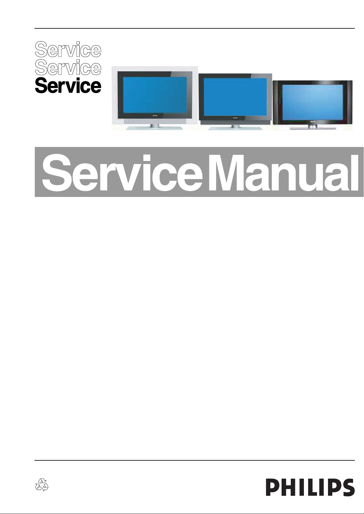
1.2 Connections
Figure 1-1 Connection overview 37PF9731/69 & 42PF9831/69
G_15990_088.eps
090506
EN 3FJ3.0E LA 1.
G_15990_085.eps
090506
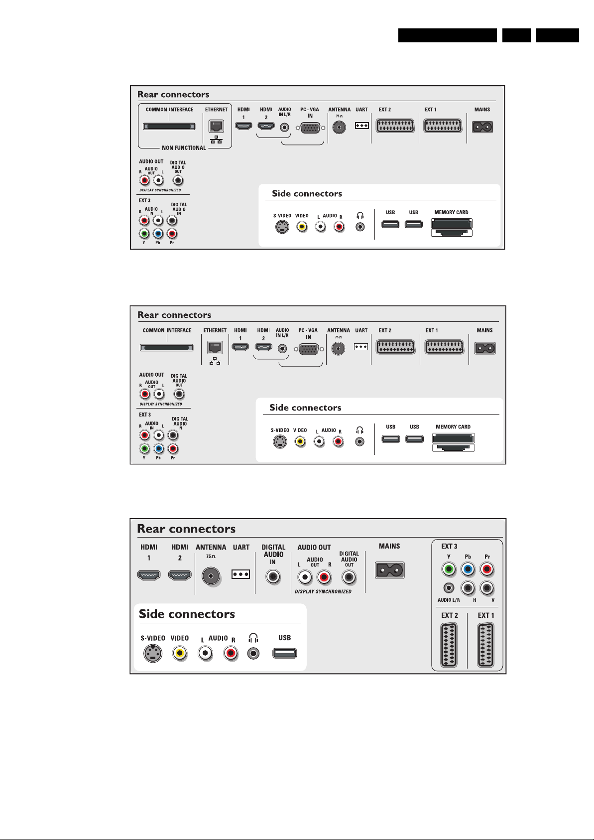
Figure 1-2 Connection overview 32PF9731D/10 & 37PF9731D/10 & 42PF9731D/10 & 42PF9831D/10
G_15990_086.eps
090506
Figure 1-3 Connection overview 32PF9531/10
EN 4 FJ3.0E LA1.
Technical Specifications, Connections, and Chassis Overview
G_15990_087.eps
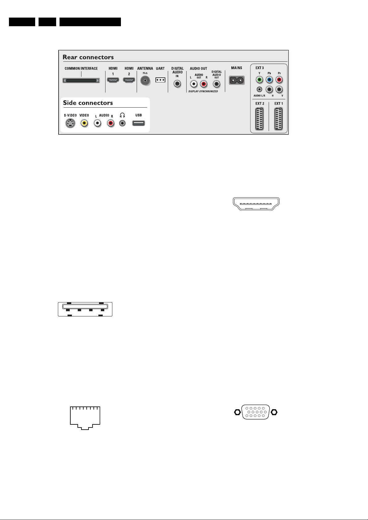
Figure 1-4 Connection overview 32PF9631D/10
090506
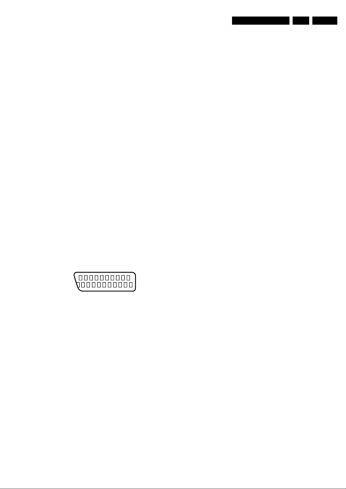
Note: The following connector colour abbreviations are used
(acc. to DIN/IEC 757): Bk= Black, Bu= Blue, Gn= Green,
Gy= Grey, Rd= Red, Wh= White, Ye= Yellow.
1.2.1 Side Connections
Headphone (Output)
Bk - Headphone 32 - 600 ohm / 10 mW ot
Cinch: Video CVBS - In, Audio - In
Rd - Audio R 0.5 V
Wh - Audio L 0.5 V
Ye - Video CVBS 1 V
/ 10 kohm jq
RMS
/ 10 kohm jq
RMS
/ 75 ohm jq
PP
SVHS (Hosiden): Video Y/C - In
1 -Ground Y Gnd H
2 -Ground C Gnd H
3 -Video Y 1 V
4 -Video C 0.3 V
/ 75 ohm j
PP
P / 75 ohm j
PP
USB2.0
1234
E_06532_022.eps
300904
Figure 1-5 USB (type A)
1-+5V k
2 -Data (-) jk
3 -Data (+) jk
4 -Ground Gnd H
1.2.2 Rear Connections
6 -RD- Receive signal j
7-n.c.
8-n.c.
HDMI 1 & 2: Digital Video, Digital Audio - In
19
18 2
1
E_06532_017.eps
250505
Figure 1-7 HDMI (type A) connector
1 -D2+ Data channel j
2 -Shield Gnd H
3 -D2- Data channel j
4 -D1+ Data channel j
5 -Shield Gnd H
6 -D1- Data channel j
7 -D0+ Data channel j
8 -Shield Gnd H
9 -D0- Data channel j
10 - CLK+ Data channel j
11 - Shield Gnd H
12 - CLK- Data channel j
13 - n.c.
14 - n.c.
15 - DDC_SCL DDC clock j
16 - DDC_SDA DDC data jk
17 - Ground Gnd H
18 - +5V j
19 - HPD Hot Plug Detect j
20 - Ground Gnd H
Cinch: Audio - In
Rd - Audio - R 0.5 V
Wh - Audio - L 0.5 V
/ 10 kohm kq
RMS
/ 10 kohm kq
RMS
RJ45: Ethernet (if present)
112345678
E_06532_025.eps
210905
Figure 1-6 Ethernet connector
1 -TD+ Transmit signal k
2 -TD- Transmit signal k
3 -RD+ Receive signal j
4-n.c.
5-n.c.
VGA: Video RGB - In
1
5
6
11
10
15
E_06532_002.eps
050404
Figure 1-8 VGA Connector
1 -Video Red 0.7 V
2 -Video Green 0.7 V
3 -Video Blue 0.7 V
4-n.c.
/ 75 ohm j
PP
/ 75 ohm j
PP
/ 75 ohm j
PP
5 -Ground Gnd H
6 -Ground Red Gnd H
7 -Ground Green Gnd H
8 -Ground Blue Gnd H
Technical Specifications, Connections, and Chassis Overview
EN 5FJ3.0E LA 1.
9-+5VDC +5 V j
10 - Ground Sync Gnd H
11 - n.c.
12 - DDC_SDA DDC data j
13 - H-sync 0 - 5 V j
14 - V-sync 0 - 5 V j
15 - DDC_SCL DDC clock j
Aerial - In
- IEC-type Coax, 75 ohm D
EXT2: Video RGB/YC - In, CVBS - In/Out, Audio - In/Out
1 -Audio R 0.5 V
2 -Audio R 0.5 V
3 -Audio L 0.5 V
4 -Ground Audio Gnd H
/ 1 kohm k
RMS
/ 10 kohm j
RMS
/ 1 kohm k
RMS
5 -Ground Blue Gnd H
6 -Audio L 0.5 V
7 -Video Blue/C-out 0.7 V
/ 10 kohm j
RMS
/ 75 ohm jk
PP
8 -Function Select 0 - 2 V: INT
4.5 - 7 V: EXT 16:9
9.5 - 12 V: EXT 4:3 j
9 -Ground Green Gnd H
10 - Easylink P50 0 - 5 V / 4.7 kohm jk
11 - Video Green/Y 0.7 V
/ 75 ohm j
PP
12 - n.c.
13 - Ground Red Gnd H
14 - Ground P50 Gnd H
15 - Video Red/C 0.7 V
16 - Status/FBL 0 - 0.4 V: INT
/ 75 ohm j
PP
1 - 3 V: EXT / 75 ohm j
17 - Ground Video Gnd H
18 - Ground FBL Gnd H
19 - Video CVBS 1 V
20 - Video CVBS/Y 1 V
/ 75 ohm k
PP
/ 75 ohm j
PP
21 - Shield Gnd H
Cinch: Audio - Out
Rd - Audio - R 0.5 V
Wh - Audio - L 0.5 V
/ 10 kohm kq
RMS
/ 10 kohm kq
RMS
Digital Audio Out: Cinch: S/PDIF - Out
Bk - Coaxial 0.4 - 0.6V
/ 75 ohm
PP
kq
EXT3: Cinch: Audio - In
Rd - Audio - R 0.5 V
Wh - Audio - L 0.5 V
/ 10 kohm kq
RMS
/ 10 kohm kq
RMS
EXT3: Digital Audio In: Cinch: S/PDIF - In
Bk - Coaxial 0.2 - 0.6V
/ 75 ohm jq
PP
EXT3: Cinch: Video YPbPr - In
Gn -Video Y 1 V
Bu - Video Pb 0.7 V
Rd - Video Pr 0.7 V
/ 75 ohm jq
PP
/ 75 ohm jq
PP
/ 75 ohm jq
PP
Service Connector (UART)
1 -UART_TX Transmit k
2 -Ground Gnd H
3 -UART_RX Receive j
EXT1: Video RGB - In, CVBS - In/Out, Audio - In/Out
21
20
E_06532_001.eps
2
1
050404
Figure 1-9 SCART connector
1 -Audio R 0.5 V
2 -Audio R 0.5 V
3 -Audio L 0.5 V
4 -Ground Audio Gnd H
/ 1 kohm k
RMS
/ 10 kohm j
RMS
/ 1 kohm k
RMS
5 -Ground Blue Gnd H
6 -Audio L 0.5 V
7 -Video Blue 0.7 V
8 -Function Select 0 - 2 V: INT
/ 10 kohm j
RMS
/ 75 ohm jk
PP
4.5 - 7 V: EXT 16:9
9.5 - 12 V: EXT 4:3 j
9 -Ground Green Gnd H
10 - Easylink P50 0 - 5 V / 4.7 kohm jk
11 - Video Green 0.7 V
12 - n.c.
/ 75 ohm j
PP
13 - Ground Red Gnd H
14 - Ground P50 Gnd H
15 - Video Red 0.7 V
/ 75 ohm j
PP
16 - Status/FBL 0 - 0.4 V: INT
1 - 3 V: EXT / 75 ohm j
17 - Ground Video Gnd H
18 - Ground FBL Gnd H
19 - Video CVBS 1 V
20 - Video CVBS 1 V
/ 75 ohm k
PP
/ 75 ohm j
PP
21 - Shield Gnd H
EN 6 FJ3.0E LA1.
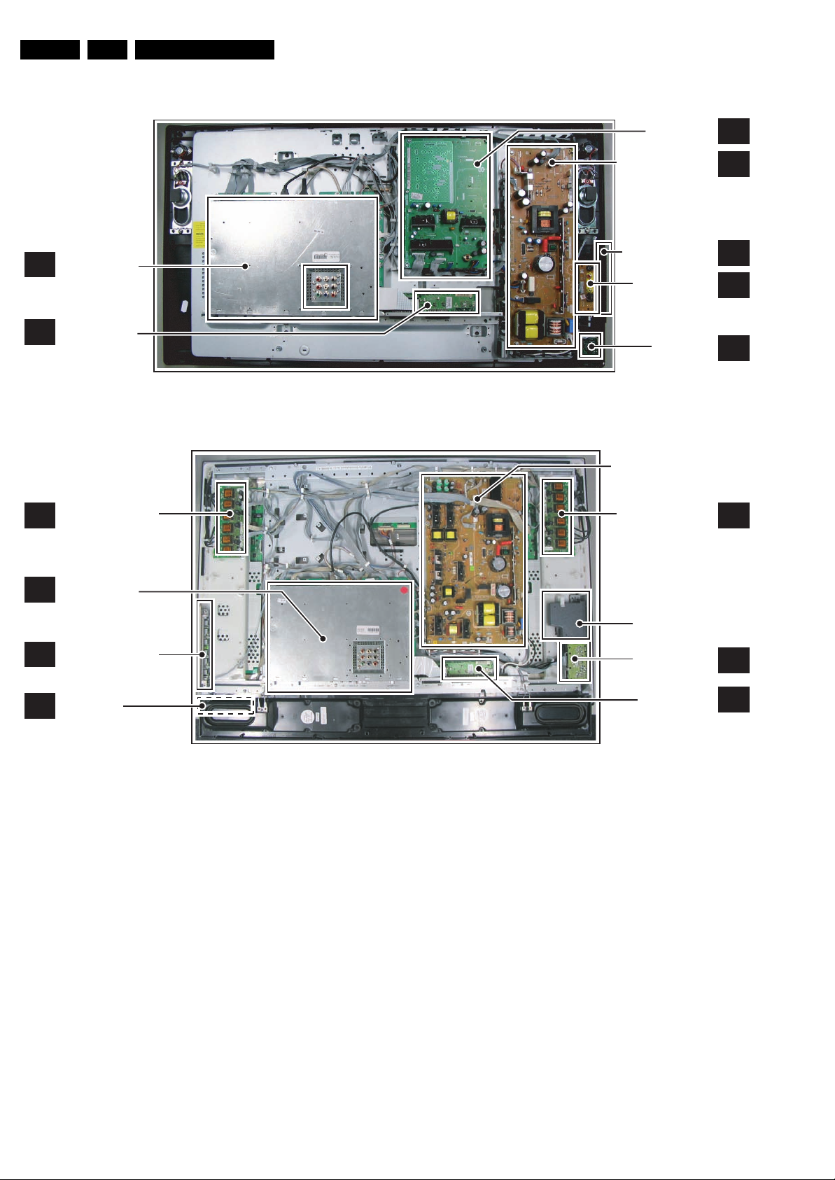
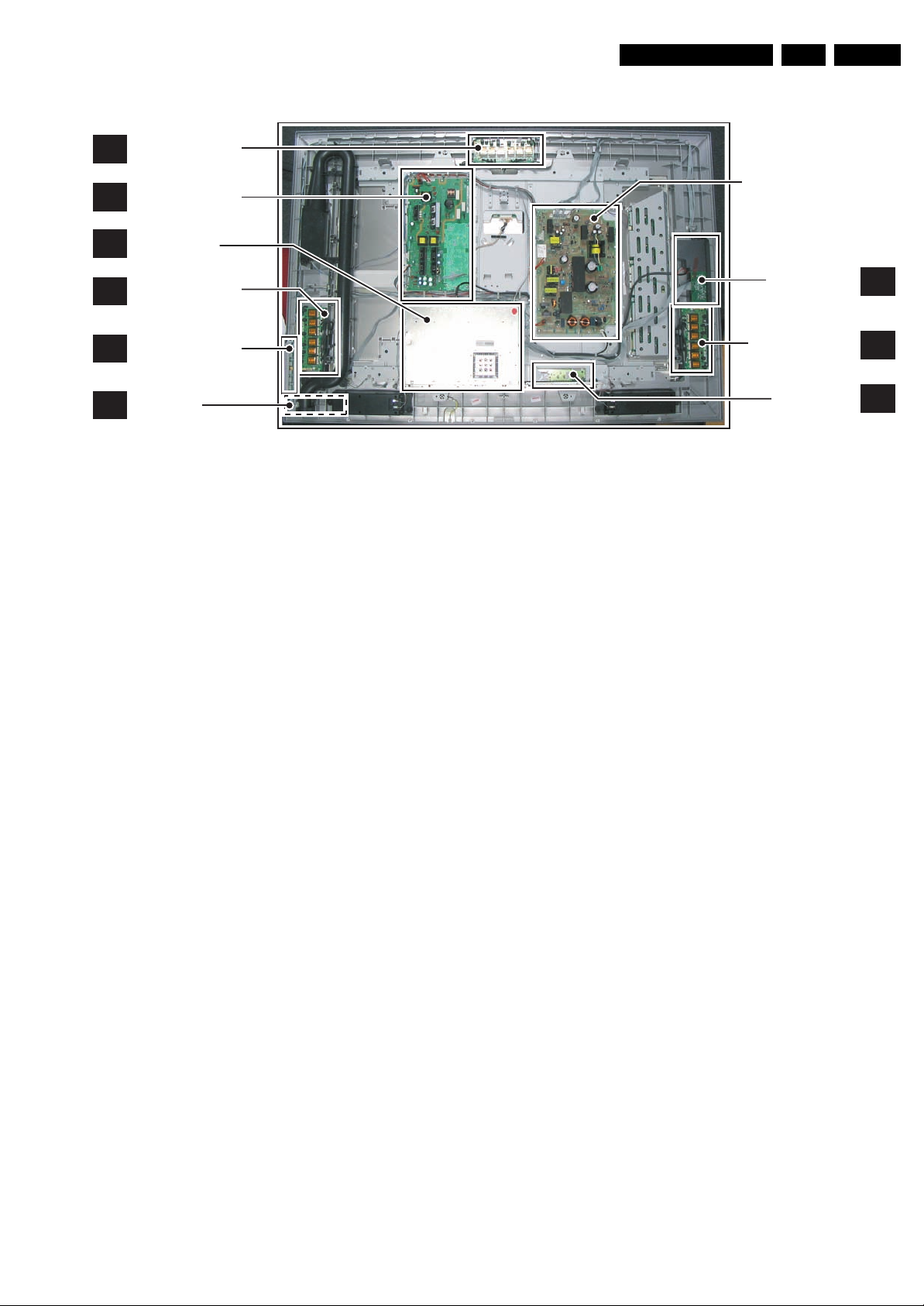
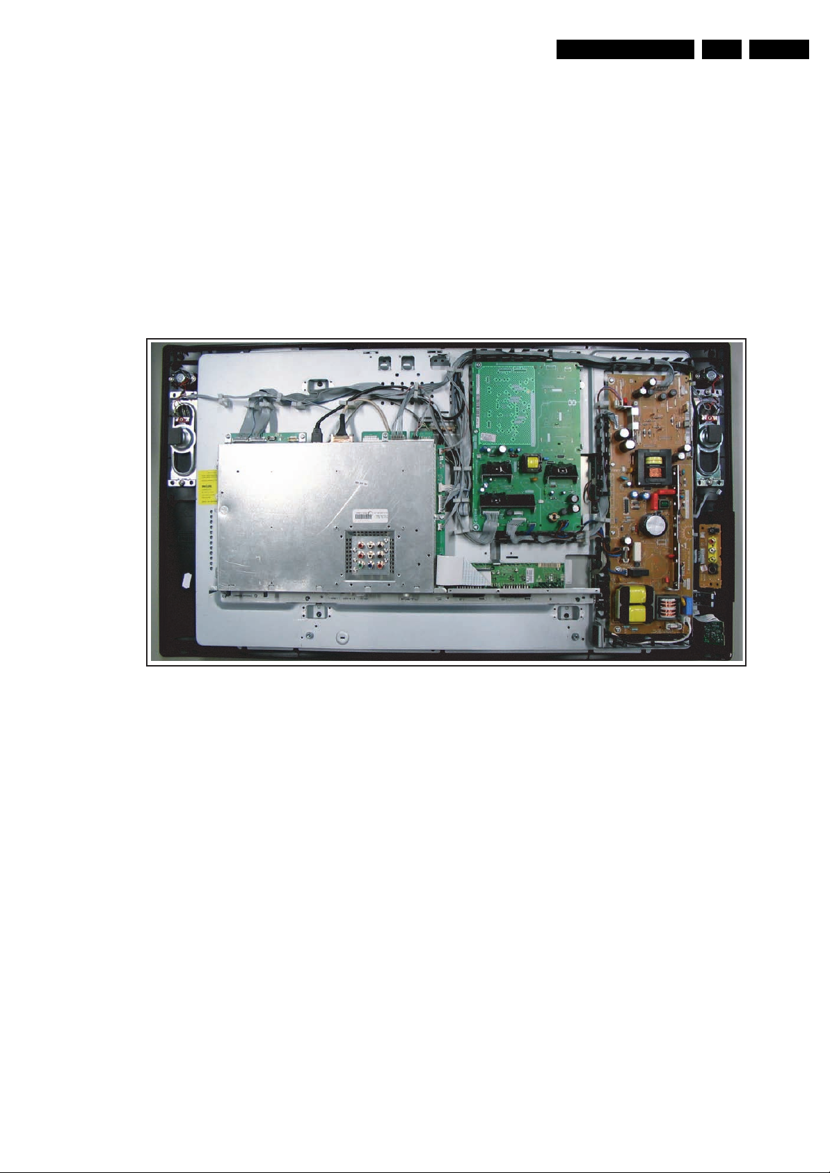
1.3 Chassis Overview
Technical Specifications, Connections, and Chassis Overview
SMALL SIGNAL
B
BOARD
EXTERNALS
BE
AMBI LIGHT PANEL
AL
G_15990_089.eps
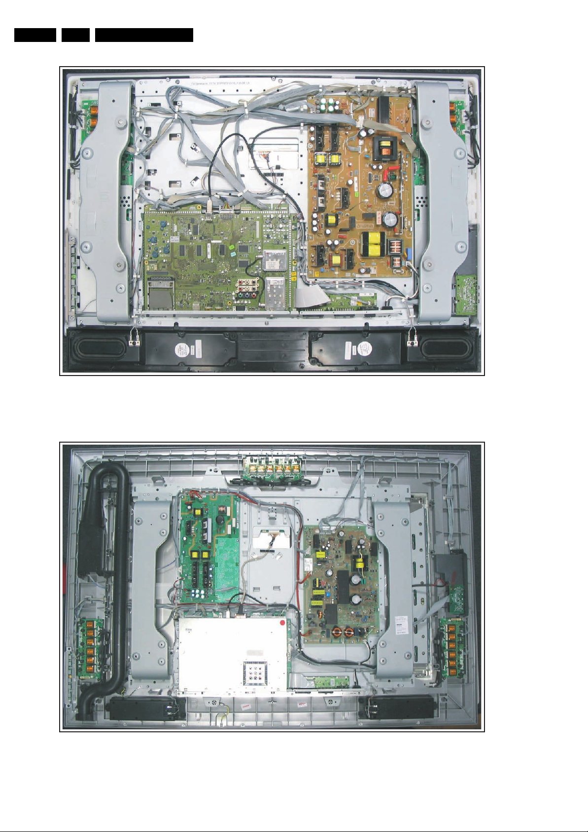
Figure 1-10 PWB/CBA locations ME6 styling (32PF9531/10 and 32PF9631D/10)
STANDBY & AUDIO
SUPPLY PANEL
CONTROL PANEL
SIDE I/O PANEL
120506
DISPLAY SUPPLY
AMBI LIGHT PANEL
PA NE L
LED PANEL
SA
A
E
D
J
AL
SMALL SIGNAL
B
BOARD
CONTROL BOARD
E
LED PANEL
J
MEMORY CARD
READER + 2x USB
SIDE I/O PANEL
EXTERNAL I/O
G_15960_143.eps
120506
Figure 1-11 PWB/CBA locations Top B styling (32PF9731D/10, 37PF9731/69, 37PF9731D/10 and 42PF9731D/10)
PA NE L
D
BE
AMBI LIGHT PANEL
AL
Technical Specifications, Connections, and Chassis Overview
EN 7FJ3.0E LA 1.
PLATFORM SUPPLY
AP
SMALL SIGNAL
B
BOARD
AMBI LIGHT PANEL
AL
CONTROL BOARD
E
LED PANEL
J
G_15960_144.eps
120506
Figure 1-12 PWB/CBA locations Top A styling (42PF9831/69 and 42PF9831D/10)
DISPLAY SUPPLY
SIDE I/O PANEL
AMBI LIGHT PANEL
EXTERNAL I/O
PA NE L
D
AL
BE

EN 8 FJ3.0E LA2.
Safety Instructions, Warnings, and Notes
2. Safety Instructions, Warnings, and Notes
Index of this chapter:
2.1 Safety Instructions
2.2 Warnings
2.3 Notes
2.1 Safety Instructions
Safety regulations require the following during a repair:
• Connect the set to the Mains/AC Power via an isolation
transformer (> 800 VA).
• Replace safety components, indicated by the symbol h,
only by components identical to the original ones. Any
other component substitution (other than original type) may
increase risk of fire or electrical shock hazard.
Safety regulations require that after a repair, the set must be
returned in its original condition. Pay in particular attention to
the following points:
• Route the wire trees correctly and fix them with the
mounted cable clamps.
• Check the insulation of the Mains/AC Power lead for
external damage.
• Check the strain relief of the Mains/AC Power cord for
proper function.
• Check the electrical DC resistance between the Mains/AC
Power plug and the secondary side (only for sets that have
a Mains/AC Power isolated power supply):
1. Unplug the Mains/AC Power cord and connect a wire
between the two pins of the Mains/AC Power plug.
2. Set the Mains/AC Power switch to the "on" position
(keep the Mains/AC Power cord unplugged!).
3. Measure the resistance value between the pins of the
Mains/AC Power plug and the metal shielding of the
tuner or the aerial connection on the set. The reading
should be between 4.5 Mohm and 12 Mohm.
4. Switch "off" the set, and remove the wire between the
two pins of the Mains/AC Power plug.
• Check the cabinet for defects, to prevent touching of any
inner parts by the customer.
2.2 Warnings
• All ICs and many other semiconductors are susceptible to
electrostatic discharges (ESD w). Careless handling
during repair can reduce life drastically. Make sure that,
during repair, you are connected with the same potential as
the mass of the set by a wristband with resistance. Keep
components and tools also at this same potential. Available
ESD protection equipment:
– Complete kit ESD3 (small tablemat, wristband,
connection box, extension cable and earth cable) 4822
310 10671.
– Wristband tester 4822 344 13999.
• Be careful during measurements in the high voltage
section.
• Never replace modules or other components while the unit
is switched "on".
• When you align the set, use plastic rather than metal tools.
This will prevent any short circuits and the danger of a
circuit becoming unstable.
2.3 Notes
2.3.1 General
• Measure the voltages and waveforms with regard to the
chassis (= tuner) ground (H), or hot ground (I), depending
on the tested area of circuitry. The voltages and waveforms
shown in the diagrams are indicative. Measure them in the
Service Default Mode (see chapter 5) with a colour bar
signal and stereo sound (L: 3 kHz, R: 1 kHz unless stated
otherwise) and picture carrier at 475.25 MHz for PAL, or
61.25 MHz for NTSC (channel 3).
• Where necessary, measure the waveforms and voltages
with (D) and without (E) aerial signal. Measure the
voltages in the power supply section both in normal
operation (G) and in stand-by (F). These values are
indicated by means of the appropriate symbols.
• The semiconductors indicated in the circuit diagram and in
the parts lists, are interchangeable per position with the
semiconductors in the unit, irrespective of the type
indication on these semiconductors.
• Manufactured under license from Dolby Laboratories.
“Dolby”, “Pro Logic” and the “double-D symbol”, are
trademarks of Dolby Laboratories.
2.3.2 Schematic Notes
• All resistor values are in ohms, and the value multiplier is
often used to indicate the decimal point location (e.g. 2K2
indicates 2.2 kohm).
• Resistor values with no multiplier may be indicated with
either an "E" or an "R" (e.g. 220E or 220R indicates 220
ohm).
• All capacitor values are given in micro-farads (µ= x10
nano-farads (n= x10
• Capacitor values may also use the value multiplier as the
decimal point indication (e.g. 2p2 indicates 2.2 pF).
• An "asterisk" (*) indicates component usage varies. Refer
to the diversity tables for the correct values.
• The correct component values are listed in the Spare Parts
List. Therefore, always check this list when there is any
doubt.
2.3.3 Rework on BGA (Ball Grid Array) ICs
General
Although (LF)BGA assembly yields are very high, there may
still be a requirement for component rework. By rework, we
mean the process of removing the component from the PWB
and replacing it with a new component. If an (LF)BGA is
removed from a PWB, the solder balls of the component are
deformed drastically so the removed (LF)BGA has to be
discarded.
Device Removal
As is the case with any component that, is being removed, it is
essential when removing an (LF)BGA, that the board, tracks,
solder lands, or surrounding components are not damaged. To
remove an (LF)BGA, the board must be uniformly heated to a
temperature close to the reflow soldering temperature. A
uniform temperature reduces the risk of warping the PWB.
To do this, we recommend that the board is heated until it is
certain that all the joints are molten. Then carefully pull the
component off the board with a vacuum nozzle. For the
appropriate temperature profiles, see the IC data sheet.
Area Preparation
When the component has been removed, the vacant IC area
must be cleaned before replacing the (LF)BGA.
Removing an IC often leaves varying amounts of solder on the
mounting lands. This excessive solder can be removed with
either a solder sucker or solder wick. The remaining flux can be
removed with a brush and cleaning agent.
After the board is properly cleaned and inspected, apply flux on
the solder lands and on the connection balls of the (LF)BGA.
Note: Do not apply solder paste, as this has been shown to
result in problems during re-soldering.
-9
), or pico-farads (p= x10
-12
-6
),
).
Safety Instructions, Warnings, and Notes
EN 9FJ3.0E LA 2.
Device Replacement
The last step in the repair process is to solder the new
component on the board. Ideally, the (LF)BGA should be
aligned under a microscope or magnifying glass. If this is not
possible, try to align the (LF)BGA with any board markers.
So as not to damage neighbouring components, it may be
necessary to reduce some temperatures and times.
More Information
For more information on how to handle BGA devices, visit this
URL: www.atyourservice.ce.philips.com (needs subscription,
not available for all regions). After login, select “Magazine”,
then go to “Repair downloads”. Here you will find Information
on how to deal with BGA-ICs.
2.3.4 Lead-free Solder
Philips CE is producing lead-free sets (PBF) from 1.1.2005
onwards.
Identification: The bottom line of a type plate gives a 14-digit
serial number. Digits 5 and 6 refer to the production year, digits
7 and 8 refer to production week (in example below it is 1991
week 18).
E_06532_024.eps
230205
avoid mixed regimes. If this cannot be avoided, carefully
clear the solder-joint from old tin and re-solder with new tin.
• Use only original spare-parts listed in the Service-Manuals.
Not listed standard material (commodities) has to be
purchased at external companies.
• Special information for lead-free BGA ICs: these ICs will be
delivered in so-called "dry-packaging" to protect the IC
against moisture. This packaging may only be opened
shortly before it is used (soldered). Otherwise the body of
the IC gets "wet" inside and during the heating time the
structure of the IC will be destroyed due to high (steam-)
pressure inside the body. If the packaging was opened
before usage, the IC has to be heated up for some hours
(around 90°C) for drying (think of ESD-protection!).
Do not re-use BGAs at all!
• For sets produced before 1.1.2005, containing leaded
soldering tin and components, all needed spare parts will
be available till the end of the service period. For the repair
of such sets nothing changes.
In case of doubt whether the board is lead-free or not (or with
mixed technologies), you can use the following method:
• Always use the highest temperature to solder, when using
SAC305 (see also instructions below).
• De-solder thoroughly (clean solder joints to avoid mix of
two alloys).
Caution: For BGA-ICs, you must use the correct temperatureprofile, which is coupled to the 12NC. For an overview of these
profiles, visit the website www.atyourservice.ce.philips.com
(needs subscription, but is not available for all regions)
You will find this and more technical information within the
"Magazine", chapter "Repair downloads".
For additional questions please contact your local repair help
desk.
Figure 2-1 Serial number example
Regardless of the special lead-free logo (which is not always
indicated), one must treat all sets from this date onwards
according to the rules as described below.
P
b
Figure 2-2 Lead-free logo
Due to lead-free technology some rules have to be respected
by the workshop during a repair:
• Use only lead-free soldering tin Philips SAC305 with order
code 0622 149 00106. If lead-free solder paste is required,
please contact the manufacturer of your soldering
equipment. In general, use of solder paste within
workshops should be avoided because paste is not easy to
store and to handle.
• Use only adequate solder tools applicable for lead-free
soldering tin. The solder tool must be able:
– To reach a solder-tip temperature of at least 400°C.
– To stabilise the adjusted temperature at the solder-tip.
– To exchange solder-tips for different applications.
• Adjust your solder tool so that a temperature of around
360°C - 380°C is reached and stabilised at the solder joint.
Heating time of the solder-joint should not exceed ~ 4 sec.
Avoid temperatures above 400°C, otherwise wear-out of
tips will increase drastically and flux-fluid will be destroyed.
To avoid wear-out of tips, switch “off” unused equipment or
reduce heat.
• Mix of lead-free soldering tin/parts with leaded soldering
tin/parts is possible but PHILIPS recommends strongly to
2.3.5 Alternative BOM identification
In September 2003, Philips CE introduced a change in the way
the serial number (or production number, see Figure 2-1) is
composed. From this date on, the third digit in the serial
number (example: AG2B0335000001) indicates the number of
the alternative BOM (Bill of Materials used for producing the
specific model of TV set). It is possible that the same TV model
on the market is produced with e.g. two different types of
displays, coming from two different O.E.M.s.
By looking at the third digit of the serial number, the service
technician can see if there is more than one type of B.O.M.
used in the production of the TV set he is working with. He can
then consult the At Your Service Web site, where he can type
in the Commercial Type Version Number of the TV set (e.g.
28PW9515/12), after which a screen will appear that gives
information about the number of alternative B.O.M.s used.
If the third digit of the serial number contains the number 1
(example: AG1B033500001), then there is only one B.O.M.
version of the TV set on the market. If the third digit is a 2
(example: AG2B0335000001), then there are two different
B.O.M.s. Information about this is important for ordering
the correct spare parts!
For the third digit, the numbers 1...9 and the characters A...Z
can be used, so in total: 9 plus 26 = 35 different B.O.M.s can
be indicated by the third digit of the serial number.
2.3.6 Practical Service Precautions
• It makes sense to avoid exposure to electrical shock.
While some sources are expected to have a possible
dangerous impact, others of quite high potential are of
limited current and are sometimes held in less regard.
• Always respect voltages. While some may not be
dangerous in themselves, they can cause unexpected
reactions that are best avoided. Before reaching into a
powered TV set, it is best to test the high voltage insulation.
It is easy to do, and is a good service precaution.

EN 10 FJ3.0E LA3.
3. Directions for Use
You can download this information from the following websites:
http://www.philips.com/support
http://www.p4c.philips.com
Directions for Use
4. Mechanical Instructions
Mechanical Instructions
EN 11FJ3.0E LA 4.
Index of this chapter:
4.1 Cable Dressing
4.2 Service Positions
4.3 Assy/Panel Removal “ME6” styling
4.4 Assy/Panel Removal “Top A” styling
4.5 Assy/Panel Removal “Top B” styling
4.6 Set Re-assembly
Notes:
• Figures below can deviate slightly from the actual situation,
due to the different set executions.
4.1 Cable Dressing
• Follow the disassemble instructions in described order.
This chassis comes with three different stylings:
• “ME6”, for type numbers 32PF9531/10 and 32PF9631D/10
• “Top B”, for type numbers 32PF9731D/10, 37PF9731/69,
37PF9731D/10 and 42PF9731D/10
• “Top A”, for type numbers 42PF9831/69 and 42PF9831D/
10.
The mechanical instructions for the different stylings are
described separately in this chapter.
Figure 4-1 Cable dressing ME6 styling (32PF9531/10 and 32PF9631D/10)
G_15990_090.eps
090506
EN 12 FJ3.0E LA4.
Mechanical Instructions
G_15990_122.eps
Figure 4-2 Cable dressing Top B styling (32PF9731D/10, 37PF9731/69, 37PF9731D/10 and 42PF9731D/10)
110506
Figure 4-3 Cable dressing Top A styling (42PF9831/69 and 42PF9831D/10)
G_15990_145.eps
120506
Mechanical Instructions
EN 13FJ3.0E LA 4.
4.2 Service Positions
For easy servicing of this set, there are a few possibilities
created:
• The buffers from the packaging.
• Foam bars (created for Service).
• Aluminium service stands (created for Service).
4.2.1 Foam Bars
E_06532_018.eps
Figure 4-4 Foam bars
The foam bars (order code 3122 785 90580 for two pieces) can
be used for all types and sizes of Flat TVs. By laying the TV
face down on the (ESD protective) foam bars, a stable situation
is created to perform measurements and alignments.
By placing a mirror under the TV, you can monitor the screen.
170504
3. Remove T10 tapping and parker screws [2] from the top,
centre, bottom, left and right side of the Rear Cover and
underneath the main I/O panel.
4. Lift the Rear Cover from the TV. Make sure that wires and
flat foils are not damaged while lifting the rear cover.
2
2
2
2
2
2
2
1
2 2
2
2
1
2
Figure 4-6 Rear cover removal
4.3.2 VESA wall plate
The VESA wall mount plate can be removed by removing the
T10 tapping screws [1] that hold the plate. See figure “VESA
wall mount plate removal”.
2
2
G_15990_091.eps
2
2
090506
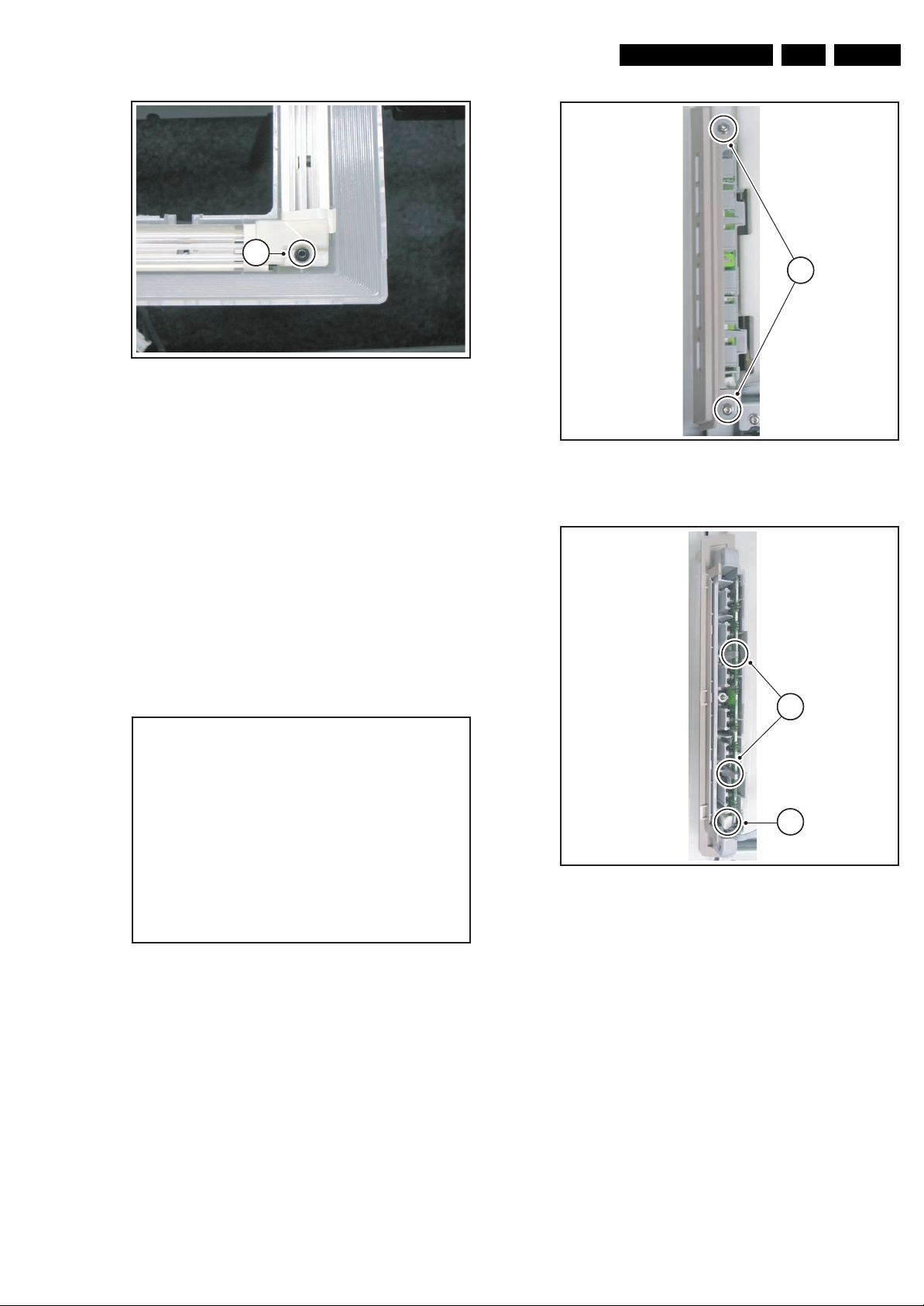
4.2.2 Aluminium Stands
E_06532_019.eps
170504
Figure 4-5 Aluminium stands (drawing of MkI)
The new MkII aluminium stands (not on drawing) with order
code 3122 785 90690, can also be used to do measurements,
alignments, and duration tests. The stands can be
(dis)mounted quickly and easyly by means of sliding them in/
out of the "mushrooms". The new stands are backwards
compatible with the earlier models.
Important: For (older) FTV sets without these "mushrooms", it
is obligatory to use the provided screws, otherwise it is possible
to damage parts inside the set !
4.3 Assy/Panel Removal “ME6” styling
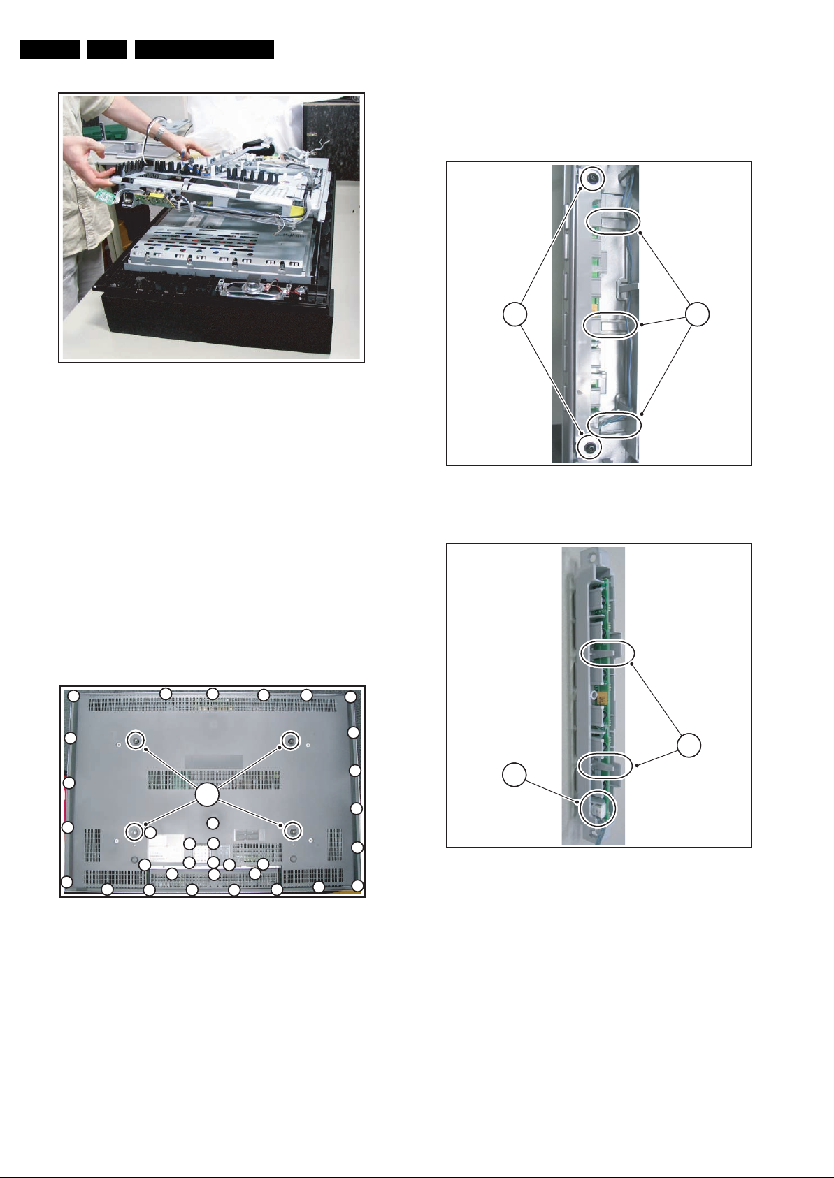
4.3.1 Rear Cover
1
Figure 4-7 VESA wall mount plate removal
4.3.3 Speaker
After removing the rear cover, you gain access to the speakers.
Caution: never disconnect the speakers with a playing set,
because otherwise the class-D audio amplifiers could be
damaged.
4.3.4 Control Panel
The Control Panel can be taken out by removing the two T10
screws [1] that hold the plastic frame. After the panel has been
taken out, the connector can be released. See figure “Control
Panel, LED Panel and Side I/O Panel removal”. When
defective, replace the whole unit.
G_15990_092.eps
090506
Disconnect the Mains/AC Power cord before you remove the
rear cover!
1. Place the TV set upside down on a table top, using the
foam bars (see part “Foam Bars”).
Caution: do not put pressure on the display, but let the
monitor lean on the Front cover.
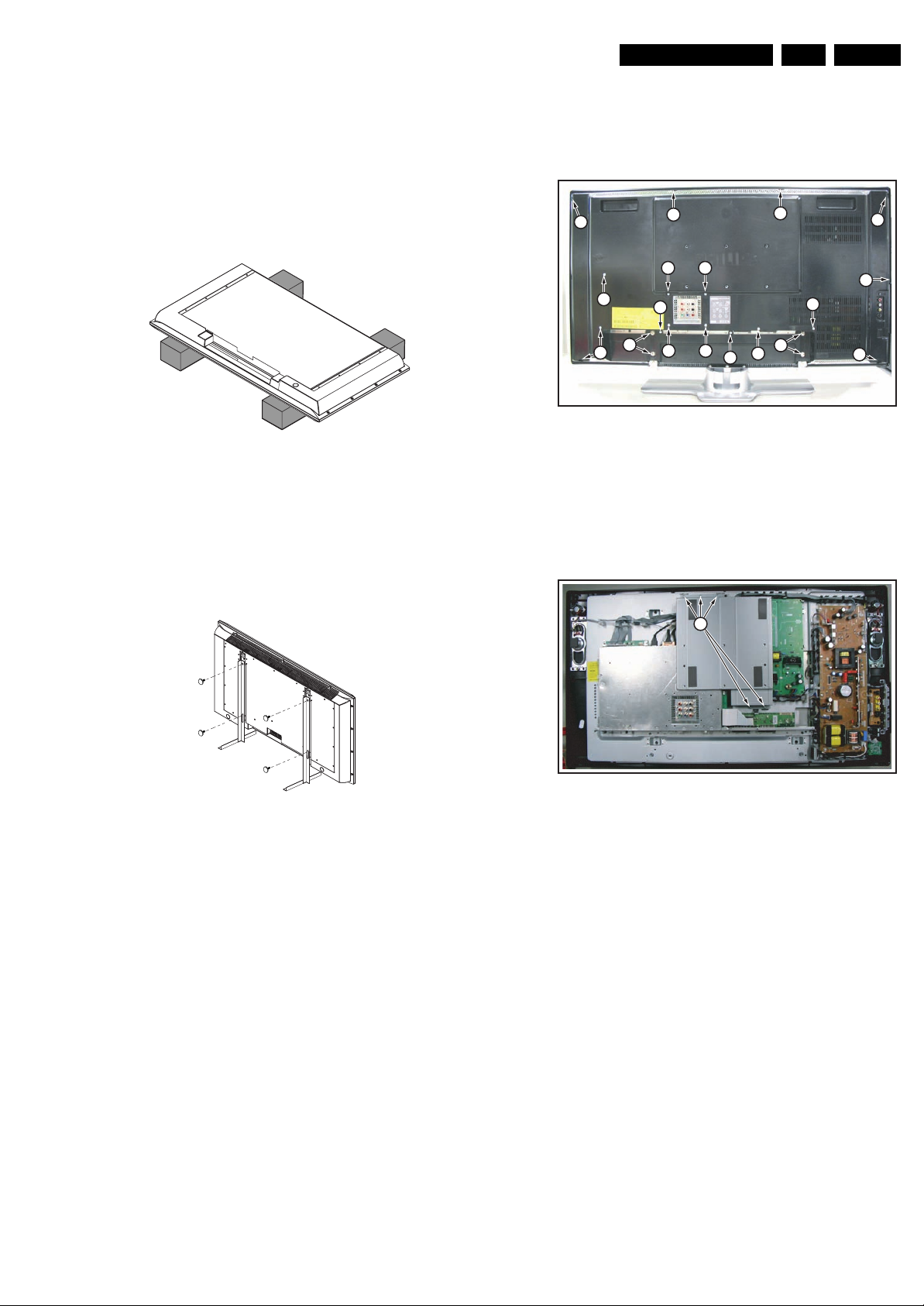
2. Remove the stand by removing the tapping screws [1], that
hold the stand.
EN 14 FJ3.0E LA4.
Mechanical Instructions
1
11
3
1
2
4
G_15990_093.eps
090506
Figure 4-10 Stand-by/Audio panel removal
4.3.8 External I/O SCART Panel
G_15990_095.eps
090506
Figure 4-8 Control panel, LED panel and side I/O panel removal
The assy is packed into a plastic frame. To take the assy out,
lift the four clamps [1] of the frame and take the assy out. See
Figure “Control panel assy removal”.
1
G_15990_094.eps
Figure 4-9 Control panel assy removal
When defective, replace the whole unit.
4.3.5 LED Panel
The LED Panel can be removed by releasing clamp [2] that
holds the assy. It hinges on the left side. See figure “Control
Panel, LED Panel and Side I/O Panel removal”.
When defective, replace the whole unit.
4.3.6 Side I/O Panel
The Side I/O Panel can be removed together with its plastic
frame. See figure “Control Panel, LED Panel and Side I/O
Panel removal”.
1. Remove the T10 parker screws [3].
2. Push back the clamps [4] on the right side that hold the
assy.
3. Take out the assy from the plastic frame, it hinges on the
left side.
When defective, replace the whole unit.
4.3.7 Stand-by/Audio Panel
090506
The External I/O SCART Panel can be taken out by removing
the flat cable and removing the parker screws [1] on the SSB
bottom shield that hold the assy. See figure “External I/O
SCART Panel removal”.
11
Figure 4-11 External I/O SCART panel
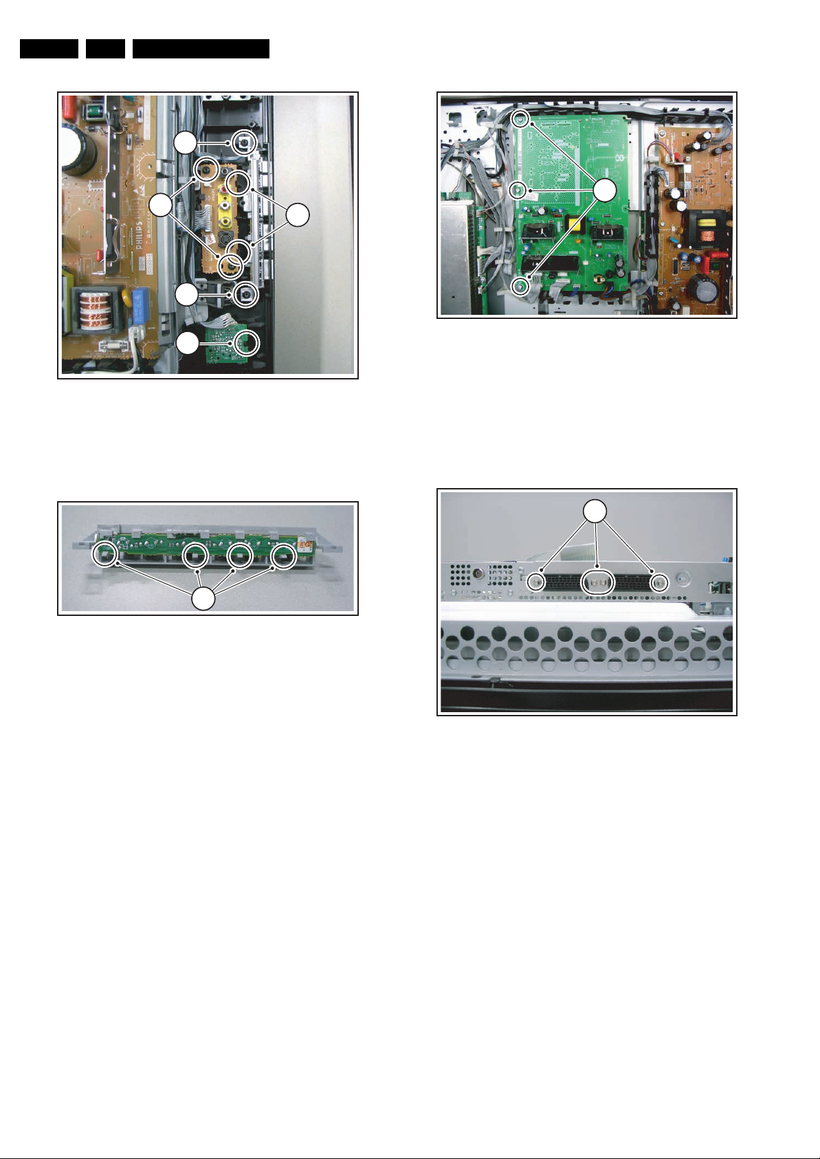
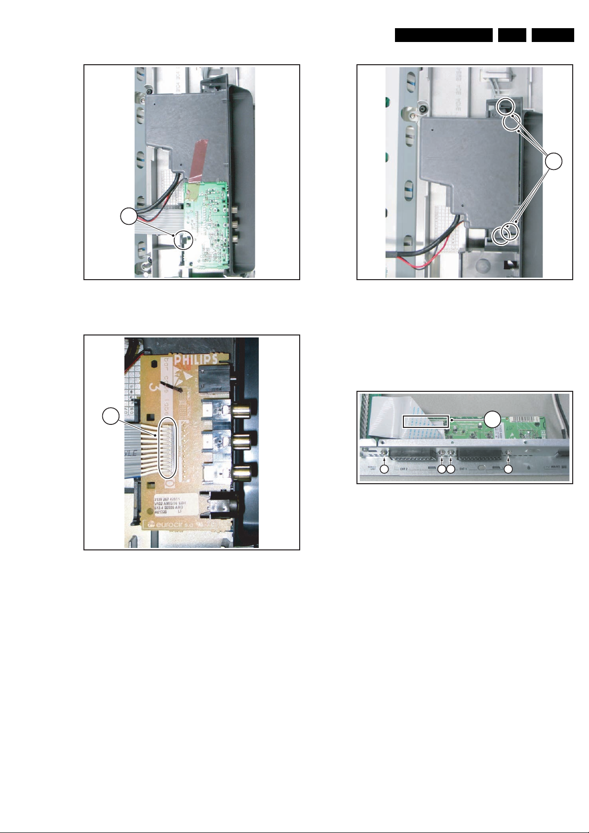
4.3.9 Small Signal Board (SSB)
Caution: it is absolutely mandatory to remount all different
screws at their original position during re-assembly. Failure to
do so may result in damaging the SSB.
Removal from the set
The SSB can, together with the External I/O SCART Panel, be
taken out of the set by removing the T10 tapping screw [1] on
the left side of the panel. See “SSB top shielding”. The frame
that holds the SSB and the External I/O SCART Panel hinges
at the right side. Disconnect all cables from the SSB before
lifting the frame from the set. This includes the USB plug and
the fragile LVDS cable.
G_15990_096.eps
090506
1. Disconnect all cables from the Stand-by/Audio Panel.
2. Remove T10 tapping screws [1] from the Stand-by/Audio
Panel. See figure “Stand-by/Audio Panel removal”.
3. Take out the Stand-by/Audio Panel (it hinges at the right
side).
Mechanical Instructions
EN 15FJ3.0E LA 4.
12
12
23
23
11
G_15990_097.eps
090506
Figure 4-12 SSB top shielding
Removing the shielding
1. Remove the T10 tapping screws [2] on the outer rim of the
SSB top shielding.
2. Remove the T10 parker screws [3] around the External I/O
SCART Panel.
3. Remove the T10 tapping screws [1] on the SSB bottom
shielding. See figure “SSB bottom shielding” for details.
1
1 1 1 1 1
1
111
1
Figure 4-14 Supply panel
1. Remove the T10 tapping screws.
2. Unplug the cables.
3. Take the panel out (it hinges on the right side).
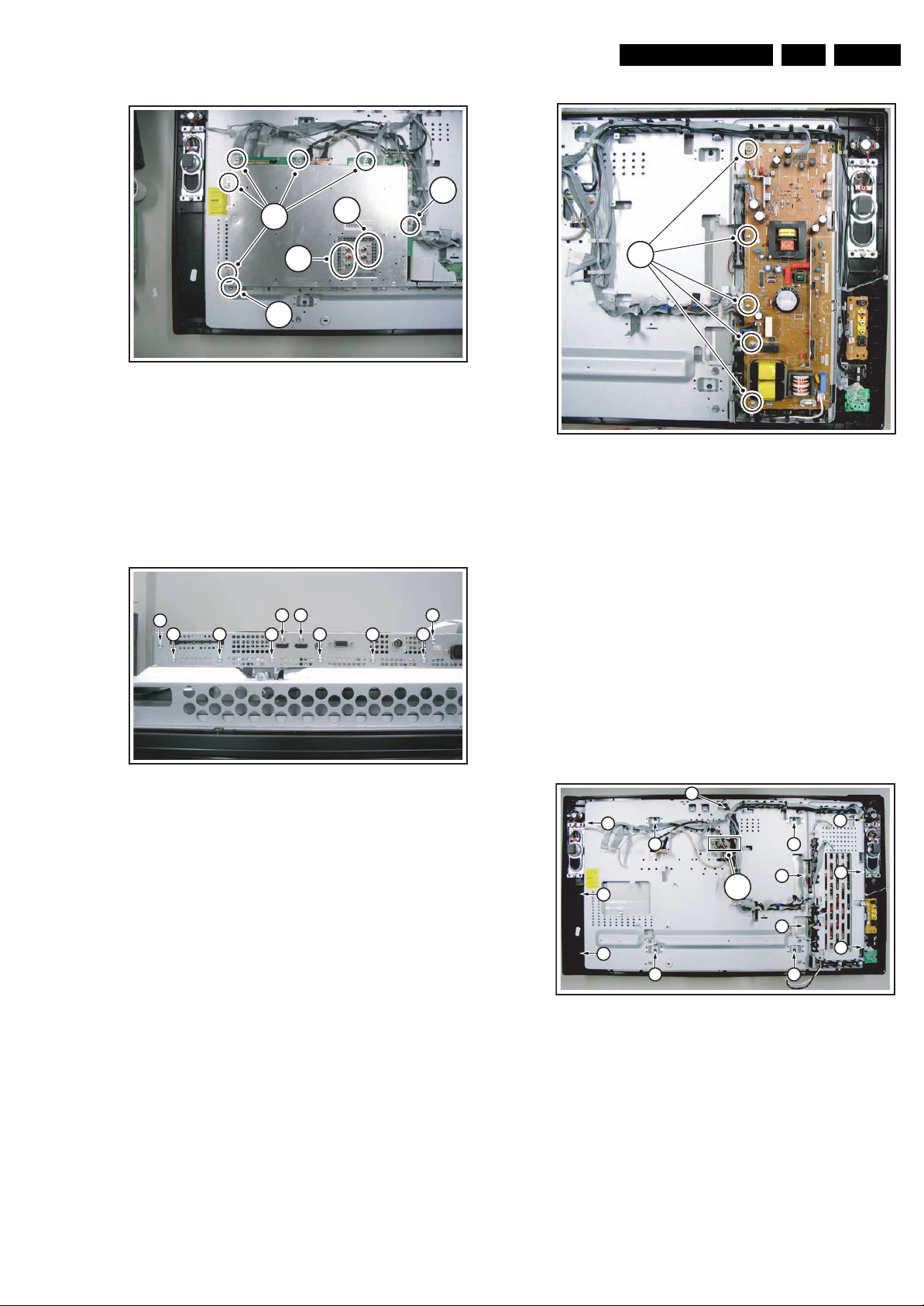
4.3.11 LCD Display Panel
For exchanging the LCD display, see figure “LCD Display
Panel removal”.
1. Remove T10 parker screws [1], indicated with an arrow on
the rim.
2. Remove T15 tapping screws [2].
3. Unplug the speaker cables.
4. Unplug the fragile LVDS connector.
5. Unplug the two connectors [4] on the LCD inverter panel.
G_15990_099.eps
090506
Figure 4-13 SSB bottom shielding
Removing the SSB and External I/O Panel
See figure “SSB and External I/O SCART Panel removal”.
• The SSB is mounted with 2 screws on the bottom shielding.
• The External I/O Panel is mounted with 4 screws on the
bottom shielding.
4.3.10 Supply Panel
See figure “Supply Panel” for details.
G_15990_098.eps
090506
1
1
1
2 2
4
1
3
1
4
1
1
2 2
G_15990_100.eps
090506
Figure 4-15 LCD display panel removal
Now the subframe can be lifted, together with the Side I/O-,
Side USB- and LED Panel. See figure “Subframe lift”. After
that, the LCD Panel can be lifted from the set.
EN 16 FJ3.0E LA4.
Mechanical Instructions
Figure 4-16 Subframe lift
4.4 Assy/Panel Removal “Top A” styling
G_15990_101.eps
090506
3. Release clips [2] and slide the unit away from the side of
the set.
4. Release clips [3] and slide the PWB out of the plastic
casing.
5. Unplug connector [4].
21
4.4.1 Rear Cover
Disconnect the Mains/AC Power cord before you remove the
rear cover!
1. Place the TV set upside down on a table top, using the
foam bars (see part “Foam Bars”).
Caution: do not put pressure on the display, but let the
monitor lean on the front cover.
2. Remove the stand.
3. Remove mushrooms [1].
4. Remove screws [2].
5. Lift the Rear Cover from the TV. Make sure that wires and
flat foils are not damaged while lifting the rear cover.
2
2
2
2
2
2
11
2
2
2
2
2
2
2
2
2
2
2
2
2
2
2
2
2
2
2
2
2
2
2
2
2
2
2
G_15990_146.eps
120506
Figure 4-18 Key control panel removal 1/2
4
Figure 4-19 Key control panel removal 2/2
When defective, replace the whole unit.
G_15990_147.eps
120506
3
G_15990_148.eps
120506
Figure 4-17 Rear cover removal
4.4.2 Speakers
After removing the rear cover, you gain access to the speakers.
Caution: never disconnect the speakers with a playing set,
because otherwise the class-D audio amplifiers could be
damaged.
4.4.3 Key Control Panel
1. Remove the rear cover, as described previously.
2. Remove screws [1].
4.4.4 Side I/O Panel
1. Remove the rear cover, as described previously.
2. Release clamp [1] and slide the PWB out of its casing.
3. Unplug connector [2] from the panel.
Mechanical Instructions
EN 17FJ3.0E LA 4.
1
1
Figure 4-20 Side I/O panel 1/2
2
Figure 4-21 Side I/O panel 2/2
G_15990_149.eps
120506
G_15990_150.eps
120506
Figure 4-22 Memory card reader / USB connector
4.4.6 External I/O SCART Panel
1. Remove the rear cover, as described previously.
2. Unplug connector [1] from the panel.
3. Remove screws [2].
1
2 2 2 2
Figure 4-23 External I/O SCART panel
4.4.7 Small Signal Board (SSB)
Caution: it is absolutely mandatory to remount all different
screws at their original position during re-assembly. Failure to
do so may result in damaging the SSB.
G_15990_151.eps
120506
G_15990_152.eps
120506
4.4.5 Memory Card reader / USB connector
1. Remove the rear cover, as described previously.
2. Release clamps [1] and slide the unit out of its plastic
frame.
3. Unplug the USB connector from the SSB panel, and the
power cable from the platform PSU.
Removal from the set
1. Remove the rear cover, as described previously.
2. Unplug connector [1] from the panel PSU.
3. Unplug all connectors [2] from the SSB panel.
4. Remove screws [3].
5. Take the complete SSB module out of the set and place it
on a flat workbench.
EN 18 FJ3.0E LA4.
Mechanical Instructions
2
1
4
3
3 3
3
G_15990_153.eps
120506
Figure 4-24 SSB panel 1/3
Removing the shielding
1. Remove screws [4] .
2. Remove the connector plate and the top shielding.
3. Remove screws [5] and remove the SSB panel from the
bottom shielding.
4
4 4 4
4 4
4 4
4 4 4
G_15990_154.eps
120506
Figure 4-25 SSB panel 2/3
2
1
2
1
2
1
2
G_15990_156.eps
120506
4
Figure 4-27 Platform supply
4.4.9 LCD Panel Supply
1. Remove the rear cover, as described previously.
2. Unplug connectors [1] from the panel.
3. Remove screws [2].
5
Figure 4-26 SSB panel 3/3
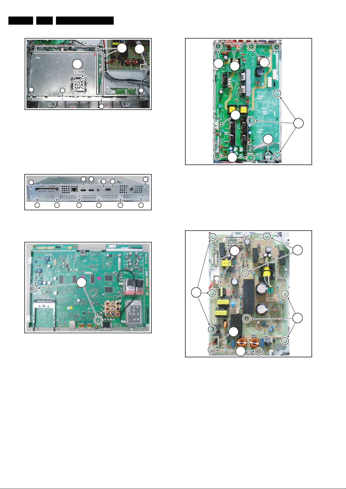
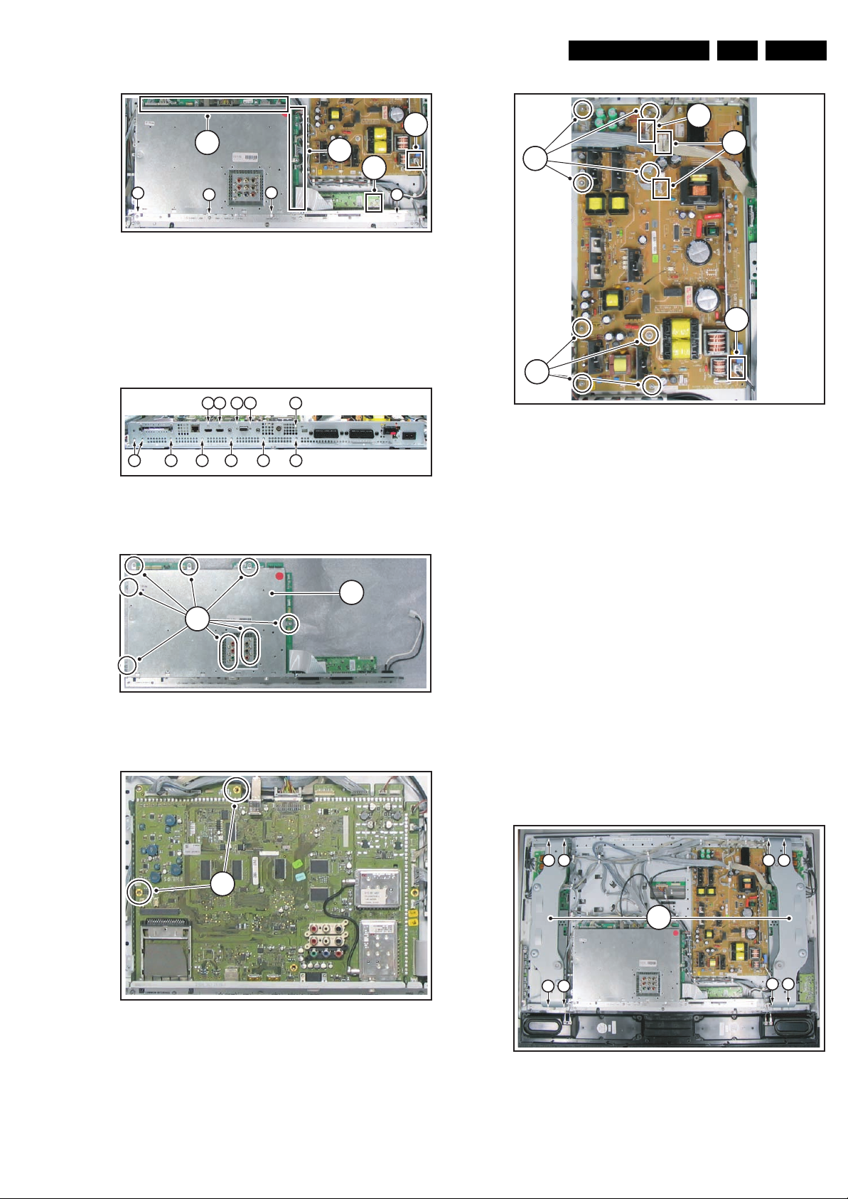
4.4.8 Platform Supply
1. Remove the rear cover, as described previously.
2. Unplug connectors [1] from the panel.
3. Remove screws [2].
G_15990_155.eps
120506
1
2
1
2
Figure 4-28 LCD panel supply
4.4.10 LCD Display Panel
For exchanging the LCD display, see figures “LCD Display
Panel removal”.
2
2
G_15990_157.eps
120506
1. Remove the rear cover, as described previously.
2. Remove the SSB module, as described previously.
3. Remove the screws [1]
4. Remove brackets [2].
5. Unplug connectors [3] from the panel PSU.
6. Unplug connector [4] from the platform PSU.
7. Unplug connectors [5] from the loudspeakers.
Mechanical Instructions
8. Unplug connectors [6] from the right hand ambilight driver
PWB.
9. Unplug earth wire [7].
10. Carefully unplug the fragile LVDS connector [8].
11. Unplug connector [9] from the X-Main PWB.
12. Remove screws [10].
13. Remove the metal subframe [11].
14. Remove screws [12].
15. Remove plastic subframe [13].
16. Release catches [14] and lift the ambilight frame [15] from
the remains of the set.
17. Remove the LCD panel [16].
14
EN 19FJ3.0E LA 4.
15
16
1 1
1 1
2
11
Figure 4-29 LCD display panel removal 1/4
10
3
10
10
8
10
4
6
11
10
5
7
10
11
G_15990_158.eps
120506
9
1010
5
G_15990_159.eps
120506
Figure 4-32 LCD Display panel removal 4/4
4.4.11 LED/IR Sensor Removal
1. Remove the LCD panel, as described previously.
2. Remove screws [1] .
3. Pull bracket [2] out of the frame.
4. Remove screws [3].
5. Pull the PWB out of the bracket.
6. Unplug connector [4].
2
1
Figure 4-33 LED/IR sensor removal 1/3
G_15990_161.eps
120506
G_15990_162.eps
120506
Figure 4-30 LCD display panel removal 2/4
12
13
Figure 4-31 LCD display panel removal 3/4
G_15990_160.eps
120506
3
Figure 4-34 LED/IR sensor removal 2/3
G_15990_163.eps
120506
EN 20 FJ3.0E LA4.
Mechanical Instructions
3
4
Figure 4-35 LED/IR sensor removal 3/3
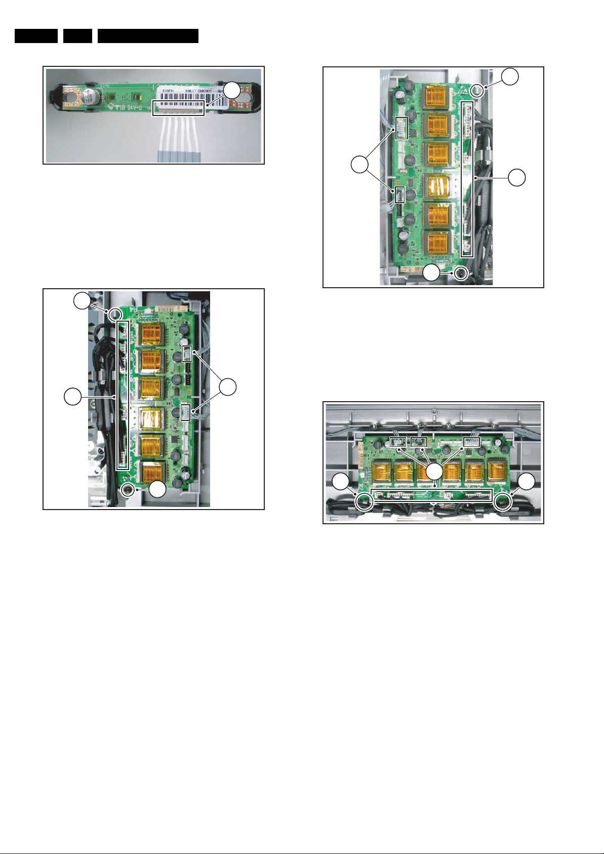
4.4.12 Ambilight Inverter Board Left
1. Remove the rear cover, as described previously.
2. Unplug connectors [1].
3. Remove screw [2].
4. Release clamp [3].
3
1
G_15990_164.eps
120506
1
1
2
Figure 4-37 Ambilight inverter board right
4.4.14 Ambilight Inverter Board Top
1. Remove the rear cover, as described previously.
2. Unplug connectors [1] .
3. Release clamp [2].
1
G_15990_166.eps
120506
2
Figure 4-36 Ambilight inverter board left
4.4.13 Ambilight Inverter Board Right
1. Remove the rear cover, as described previously.
2. Unplug connectors [1] .
3. Remove screw [2].
4. Release clamp [3].
G_15990_165.eps
120506
22
2
Figure 4-38 Ambilight inverter board top
4.4.15 Ambilight Module
1. Carry out the disassembly “LCD Display Panel”, except for
the last point.
2. Put the ambilight frame on a flat workbench.
3. Remove screws [1].
1
G_15990_167.eps
120506
1
Figure 4-39 Ambilight module
Mechanical Instructions
G_15990_168.eps
120506
EN 21FJ3.0E LA 4.
1
4.5 Assy/Panel Removal “Top B” styling
4.5.1 Rear Cover
Disconnect the Mains/AC Power cord before you remove the
rear cover!
1. Place the TV set upside down on a table top, using the
foam bars (see part “Foam Bars”).
Caution: do not put pressure on the display, but let the
monitor lean on the front cover.
2. Remove the stand.
3. Remove mushrooms [1].
4. Remove screws [2].
5. Lift the Rear Cover from the TV. Make sure that wires and
flat foils are not damaged while lifting the rear cover.
Not yet available
Figure 4-41 Key control panel removal 1/2
2
3
Figure 4-42 Key control panel removal 2/2
G_15990_124.eps
110506
G_15990_125.eps
110506
Figure 4-40 Rear cover removal
4.5.2 Speakers
After removing the rear cover, you gain access to the speakers.
Caution: never disconnect the speakers with a playing set,
because otherwise the class-D audio amplifiers could be
damaged.
4.5.3 Key Control Panel
1. Remove the rear cover, as described previously.
2. Remove screws [1].
3. Release clips [2] and slide the PWB out of the plastic
casing.
4. Unplug connector [3].
G_15990_123.eps
120506
When defective, replace the whole unit.
4.5.4 Side I/O Panel
1. Remove the rear cover, as described previously.
2. Release clamp [1] and slide the PWB out of its casing.
3. Unplug connector [2] from the panel.
EN 22 FJ3.0E LA4.
Mechanical Instructions
1
1
Figure 4-43 Side I/O panel 1/2
2
Figure 4-44 Side I/O panel 2/2
4.5.5 Memory Card reader / USB connector
1. Remove the rear cover, as described previously.
2. Release clamps [1] and slide the unit out of its plastic
frame.
3. Unplug the USB connector from the SSB panel, and the
power cable from the PSU.
G_15990_126.eps
110506
G_15990_127.eps
110506
Figure 4-45 Memory card reader / USB connector
4.5.6 External I/O SCART Panel
1. Remove the rear cover, as described previously.
2. Unplug connectors [1] from the panel.
3. Remove screws [2].
1
2 2 2 2 2 2
Figure 4-46 External I/O SCART panel
4.5.7 Small Signal Board (SSB)
Caution: it is absolutely mandatory to remount all different
screws at their original position during re-assembly. Failure to
do so may result in damaging the SSB.
Removal from the set
1. Remove the rear cover, as described previously.
2. Unplug all connectors [1] from the SSB panel.
3. Unplug connector [2] from the PSU.
4. Remove screws [3].
5. Take the complete SSB module out of the set and place it
on a flat workbench.
G_15990_128.eps
110506
G_15990_129.eps
110506
Mechanical Instructions
EN 23FJ3.0E LA 4.
2
1
1
1
3
3
3
3
G_15990_130.eps
110506
Figure 4-47 SSB panel 1/4
Removing the shielding
1. Remove screws [4] .
2. Remove the connector plate [5] and the top shielding [6].
3. Remove screws [7] and remove the SSB panel from the
bottom shielding.
4 4 4 4 5
4 4 4 4 4 4
G_15990_131.eps
110506
Figure 4-48 SSB panel 2/4
1
2
2
Figure 4-51 Platform supply
4.5.9 LCD Display Panel
For exchanging the LCD display, see figures “LCD Display
Panel removal”.
1
1
G_15990_134.eps
110506
4
Figure 4-49 SSB panel 3/4
7
6
G_15990_132.eps
110506
1. Remove the rear cover, as described previously.
2. Remove screws [1]
3. Remove brackets [2].
4. Unplug LVDS connector [3] from the panel.
5. Unplug connector [4] of the IR/LED panel from the SSB.
6. Unplug connectors [5] from the loudspeakers.
7. Unplug connectors [6] from the ambilight inverter PWB.
8. Remove screws [7] and put the key control unit on the
subframe.
9. Release the Mem. Card Reader/Side I/O [8] and put it on
the subframe.
10. Unplug connector [9] from the X-Main PWB.
11. Remove screws [10].
12. Remove the subframe [11].
13. Remove screws [12].
14. Remove brackets [13] and plastic ambilight frame [14].
15. Remove the LCD panel [15].
1 11 1
2
Figure 4-50 SSB panel 4/4
4.5.8 Power Supply
1. Remove the rear cover, as described previously.
2. Unplug connectors [1] from the panel.
3. Remove screws [2].
G_15990_133.eps
110506
11
Figure 4-52 LCD Display panel removal 1/4
11
G_15990_135.eps
110506
EN 24 FJ3.0E LA4.
Mechanical Instructions
10
6
3
10
9
4
7
5 5
7
1010
Figure 4-53 LCD display panel removal 2/4
312
14
6
8
G_15990_136.eps
120506
13
1
Figure 4-56 LED/IR sensor removal
4.5.11 Ambilight Inverter Boards
1. Remove the rear cover, as described previously.
2. Remove the metal bracket, that is mounted over the
Inverter Board you want to replace, as described
previously.
3. Unplug connectors [1] .
4. Release clamps [2].
2
2
G_15990_139.eps
110506
Figure 4-54 LCD display panel removal 3/4
15
Figure 4-55 LCD display panel removal 4/4
13
G_15990_137.eps
120506
G_15990_138.eps
110506
1
2
Figure 4-57 Ambilight inverter board
4.5.12 Ambilight Module
1. Carry out the disassembly “LCD Display Panel”, except for
the last point.
2. Put the ambilight frame on a flat workbench.
3. Remove screws [1].
G_15990_140.eps
110506
4.5.10 LED/IR Sensor Removal
1. Carry out the disassembly of the LCD panel, as described
previously, except for the last point.
2. Remove screws [1] .
3. Unplug connector [2].
1
Figure 4-58 Ambilight module
Mechanical Instructions
G_15990_141.eps
110506
EN 25FJ3.0E LA 4.
4.6 Set Re-assembly
To re-assemble the whole set, execute all processes in reverse
order.
Notes:
• While re-assembling, make sure that all cables are placed
and connected in their original position. See figure "Cable
dressing".
• Pay special attention not to damage the EMC foams on the
SSB shields. Ensure that EMC foams are mounted
correctly.
EN 26 FJ3.0E LA5.
s
6
Service Modes, Error Codes, and Fault Finding
5. Service Modes, Error Codes, and Fault Finding
Index of this chapter:
5.1 Test Points
5.2 Service Modes
5.3 Stepwise Start-up
5.5 Error Codes
5.6 The Blinking LED Procedure
5.7 Protections
5.8 Fault Finding and Repair Tips
5.9 Software Upgrading
5.1 Test Points
The chassis is equipped with test points (Fxxx) printed on the
circuit board assemblies. As most signals are digital, it will be
difficult to measure waveforms with a standard oscilloscope.
Several key ICs are capable of generating test patterns, which
can be controlled via ComPair. In this way it is possible to
determine which part is defective.
Perform measurements under the following conditions:
• Service Default Mode.
• Video: Colour bar signal.
• Audio: 3 kHz left, 1 kHz right.
5.2 Service Modes
Service Default mode (SDM) and Service Alignment Mode
(SAM) offers several features for the service technician, while
the Customer Service Mode (CSM) is used for communication
between the call centre and the customer.
This chassis also offers the option of using ComPair, a
hardware interface between a computer and the TV chassis. It
offers the abilities of structured troubleshooting, error code
reading, and software version read-out for all chassis.
Minimum requirements for ComPair: a Pentium processor, a
Windows OS, and a CD-ROM drive (see also paragraph
"ComPair").
• All service-unfriendly modes (if present) are disabled, like:
– (Sleep) timer.
– Child/parental lock.
– Picture mute (blue mute or black mute).
– Automatic volume levelling (AVL).
– Auto switch "off" (when no video signal was received
for 10 minutes).
– Skip/blank of non-favourite pre-sets.
– Smart modes.
– Auto store of personal presets.
– Auto user menu time-out.
How to Activate SDM
For DVBT TV’s there are two kinds of SDM : an analogue SDM
and a digital SDM. Tuning will happen according table “SDM
Default Settings”.
• Analogue SDM: use the standard RC-transmitter and key
in the code “062596”, directly followed by the “MENU”
button.
Note: It is possible that, together with the SDM, the main
menu will appear. To switch it "off", push the “MENU”
button again.
• Digital SDM: use the standard RC-transmitter and key in
the code “062593”, directly followed by the “MENU” button.
Depending on the software version it is possible that the
tuning will not work correctly.
Note: It is possible that, together with the SDM, the main
menu will appear. To switch it "off", push the “MENU”
button again.
• Analogue SDM can also be activated by shorting for a
moment the two solder pads [1] on the SSB, with the
indication “SDM”. They are located outside the shielding.
Activation can be performed in all modes, except when the
set has a problem with the Stand-by Processor. See figure
“Service mode pads”.
SDM
SDM
11
5.2.1 Service Default Mode (SDM)
Purpose
• To create a pre-defined setting, to get the same
measurement results as given in this manual.
• To override SW protections detected by stand-by
processor and make the TV start up to the step just before
protection (a sort of automatic stepwise start up). See
paragraph “Stepwise Start Up”.
• To override SW protections detected by Viper. Depending
on the SW version it is possible that this mechanism does
not work correctly. See also paragraph “Error codes”.
• To start the blinking LED procedure (not valid in protection
mode).
Specifications
Table 5-1 SDM default settings
Region Freq. (MHz)
Europe, AP(PAL/Multi) 475.25 PAL B/G
Europe, AP DVBT 546.000
PID Video: 0B 06
PID PCR: 0B 06
PID Audio: 0B 07
• All picture settings at 50% (brightness, colour, contrast).
• All sound settings at 50%, except volume at 25%.
Default
system
DVBT
12
SPISPI
G_15990_142.ep
11050
Figure 5-1 Service mode pads
After activating this mode, “SDM” will appear in the upper right
corner of the screen (if you have picture).
How to Navigate
When you press the “MENU” button on the RC transmitter, the
set will toggle between the SDM and the normal user menu
(with the SDM mode still active in the background).
How to Exit SDM
Use one of the following methods:
• Switch the set to STAND-BY via the RC-transmitter.
Service Modes, Error Codes, and Fault Finding
EN 27FJ3.0E LA 5.
• Via a standard customer RC-transmitter: key in “00”sequence.
5.2.2 Service Alignment Mode (SAM)
Purpose
• To perform (software) alignments.
• To change option settings.
• To easily identify the used software version.
• To view operation hours.
• To display (or clear) the error code buffer.
How to Activate SAM
Via a standard RC transmitter: key in the code “062596”
directly followed by the “INFO” button. After activating SAM
with this method a service warning will appear on the screen,
you can continue by pressing the red button on the RC.
Contents of SAM:
• Hardware Info.
– A. SW Version. Displays the software version of the
VIPER software (main software) (example: JA30E-
1.2.3.4_12345 = AAAAB_X.Y.W.Z_NNNNN).
• AAAA= the software name.
• B= the region: A= AP, E= EU, L= LatAm, U = US.
For AP sets it is possible that the Europe software
version is used.
• X.Y.W.Z= the software version, where X is the
main version number (different numbers are not
compatible with one another) and Y.W.Z is the sub
version number (a higher number is always
compatible with a lower number).
• NNNNN= last five digits of 12nc code of the
software.
– B. SBY PROC Version. Displays the software version
of the stand-by processor.
– C. Production Code. Displays the production code of
the TV, this is the serial number as printed on the back
of the TV set. Note that if an NVM is replaced or is
initialized after corruption, this production code has to
be re-written to NVM. ComPair will foresee in a
possibility to do this.
• Operation Hours. Displays the accumulated total of
operation hours (not the stand-by hours). Every time the
TV is switched "on/off", 0.5 hours is added to this number.
• Errors. (Followed by maximal 10 errors). The most recent
error is displayed at the upper left (for an error explanation
see paragraph “Error Codes”).
• Defective Module. Here the module that generates the
error is displayed. If there are multiple errors in the buffer,
which are not all generated by a single module, there is
probably another defect. It will then display the message
“UNKNOWN” here. Not all errors will display a defective
module name.
• Reset Error Buffer. When you press “cursor right” and
then the “OK” button, the error buffer is reset.
• Alignments. This will activate the “ALIGNMENTS” submenu.
• Dealer Options. Extra features for the dealers.
• Options. Extra features for Service. For more info
regarding option codes, see chapter 8.
Note that if you change the option code numbers, you have
to confirm your changes with the “OK” button before you
store the options. Otherwise you will lose your changes.
• Initialise NVM. When an NVM was corrupted (or replaced)
in the former EMG based chassis, the microprocessor
replaces the content with default data (to assure that the
set can operate). However, all preferences and alignment
values are gone now, and option numbers are not correct.
Therefore, this was a very drastic way. In this chassis, the
procedure is implemented in another way: The moment the
processor recognizes a corrupted NVM, the “initialize
NVM” line will be highlighted. Now, you can do two things
(depending of the service instructions at that moment):
– Save the content of the NVM via ComPair for
development analysis, before initializing. This will give
the Service department an extra possibility for
diagnosis (e.g. when Development asks for this).
– Initialize the NVM (same as in the past, however now it
happens conscious).
Note: When you have a corrupted NVM, or you have replaced
the NVM, there is a high possibility that you will not have picture
any more because your display option is not correct. So, before
you can initialize your NVM via the SAM, you need to have
picture and therefore you need the correct display option. To
adapt this option, you can use ComPair (the correct HEX
values for the options can be found in the table below) or a
method via a standard RC (described below).
Changing the display option via a standard RC:
Key in the code “062598” directly followed by the “MENU”
button and “XXX” (where XXX is the 3 digit decimal display
option code as mentioned in the first column of the next table).
Make sure to key in all three digits, also the leading zero’s.
If the above action is successful, the front LED will go out as an
indication that the RC sequence was correct.
After the display option is changed in the NVM, the TV will go
to the Stand-by mode.
If the NVM was corrupted or empty before this action, it will be
initialised first (loaded with default values). This initialising can
take up to 20 seconds.
Table 5-2 Display option code overview
Display
HEX Display Type Display Code Number Size Vertical
Option
000 00 PDP SDI HD V3 V3_SA42AX-****-
001 01 PDP SDI HD V3 V3-S50HW-XD03-
002 02 PDP FHP A1-
003 03 LCD LPL LC300W01-A3P7-
004 04 LCD LPL LC370W01-A6K1-
005 05 LCD LPL LC420W02-A6-v1.0 42” 768p
006 06 LCD SHARP ASV1-
007 07 PDP SDI SD V3 V3_S42SD-YD05-
008 08 PDP FHP A1_PFP37C128128U
009 09 LCOS XION Xion1,05- v0.01 - 720p
010 0A LCD AUO T296XW01-v0.5 30” 768p
011 0B LCD LPL LC32CW01-A6K1v1.0 32” 768p
012 0C LCD AUO T315XW01V0-v0.1 32” 768p
013 0D LCD SHARP ASV2_LQ370T3LZ21
014 0E LCD LPL full HD LC420WU1-SL01-
015 0F PDP SDI SD 37” 480p
016 10 PDP FHP 37” 1080i
017 11 PDP FHP tbf 42” 1080i
018 12 PDP FHP FPF55C17196UA-51-
019 13 LCOS VENUS - 720p
020 14 LCOS VENUS full HD - 1080p
021 15 LCD LPL LC260WX2-SL01-
022 16 LCD LPL clear LCD LC320WX2-SL01 32” 768p
023 17 PDP LG SD PDP42x2-56-Rev.00 42” 480p
024 18 PDP SDI V4 V4-S42SD-YD07-v0.0 42” 480p
025 19 PDP SDI V4 V4-S42AX-YD01-
026 1A PDP FHP A2 FPF42C128128UD-51 42” 1024i
027 1B PDP SDI HD V4 V4-S50HW-XD04-
028 1C LCD Sharp full HD LQ370D3LZ1x
029 1D LCD AUO T315XW01-V3-V0.1 32” 768p
030 1E for development sam-
ple only
Rev,2
v0,0
FPF42C128128UC52-v01
v2.1
v1.0
LQ315T3LZ13ASV2.2
v0.2
B-71-v0.1
ASV2.2LQ370T3LZ44
v0.0
v04
v1,0
Rev0.1
v0.2
ASV2.2
LW370D3LZ1xASV3.
0 (first sample)
Resolution
42” 768p
50” 768p
42” 1024i
30” 768p
37” 768p
32” 768p
42” 480p
37” 1024i
37” 768p
42” 1080p
55” 768p
26” 768p
42” 768p
50” 768p
37” 1080p

EN 28 FJ3.0E LA5.
Service Modes, Error Codes, and Fault Finding
Display
HEX Display Type Display Code Number Size Vertical
Option
031 1F LCD Sharp full HD
032 20 LCD LPL LC200WX1-SL01 20” 768p
033 21 LCD QDI QD23HL 23” 768p
034 22 ECO PTV 51” 1080i
035 23 ECO PTV 55” 1080i
036 24 ECO PTV 61” 1080i
037 25 PDP FHP A3 FPF42128135UA 42” 1024i
038 2 6 DLP tbf 50” 720p
039 2 7 DLP tbf 60” 720p
040 28 LCD Sharp V2.3 ASV 2.3 32” 768p
041 29 LCD LPL clear LCD LC420WX2-SLA1 42” 768p
042 2A PDP SDI V4 63” 768p
043 2B LCD Sharp V3.0 clear
044 2C LCD Sharp V2.3 37” 768p
045 2D LCD LPL 26” 768p
046 2E LCD LPL 32” 768p
clear LCD V3.0
LCD
LQ370D3LZ1x
ASV3.0
Resolution
37” 1080p
37” 768p
• Store. All options and alignments are stored when
pressing “cursor right” and then the “OK”-button
• SW Maintenance.
– SW Events. Not useful for Service purposes. In case
of specific software problems, the development
department can ask for this info.
– HW Events. Not useful for Service purposes. In case
of specific software problems, the development
department can ask for this info.
5.2.3 Customer Service Mode (CSM)
Purpose
When a customer is having problems with his TV-set, he can
call his dealer or the Customer Helpdesk. The service
technician can then ask the customer to activate the CSM, in
order to identify the status of the set. Now, the service
technician can judge the severity of the complaint. In many
cases, he can advise the customer how to solve the problem,
or he can decide if it is necessary to visit the customer.
The CSM is a read only mode; therefore, modifications in this
mode are not possible.
When in this chassis, CSM is activated, a colour bar test
pattern will be visible for 5 seconds. This test pattern is
generated by the Pacific3. So if you see this test pattern you
can determine that the back end video chain (Pacific3, LVDS
and display) is working.
Also new in this chassis: when you activate CSM and there is
a USB stick connected to the TV, the software will dump the
complete CSM content to the USB stick. The file (Csm.txt) will
be saved in the root of your USB stick. This info can be handy
if you don’t have picture.
How to Activate CSM
Key in the code “123654” via the standard RC transmitter.
Note: Activation of the CSM is only possible if there is no (user)
menu on the screen!
• Operating hours. Here you are able to reset
the operations hours of the display. This has to be done in
case of replacement of the display.
• Upload to USB. Here you are able to upload several
settings from the TV to a USB stick which is connected to
the Side IO. The four items are “Channel list”, “Personal
settings”, “Option codes” and “Display-related alignments”.
First you have to create a directory “repair\” in the root of
the USB stick.To upload the settings you have to select
each item separately, press “cursor right”, confirm with
“OK” and wait until “Done” appears. Now the settings are
stored onto your USB stick and can be used to download
onto another TV or other SSB. Uploading is of course only
possible if the software is running and if you have picture.
This method is created to be able to save the customer’s
TV settings and to store them into another SSB.
• Download from USB. Here you are able to download
several settings from the USB stick to the TV. Same way of
working as with uploading. To make sure that the download
of the channel list from USB to the TV is executed properly,
it is necessary to restart the TV and tune to a valid preset if
necessary.
How to Navigate
• In SAM, you can select the menu items with the “CURSOR
UP/DOWN” key on the RC-transmitter. The selected item
will be highlighted. When not all menu items fit on the
screen, move the “CURSOR UP/DOWN” key to display the
next/previous menu items.
• With the “CURSOR LEFT/RIGHT” keys, it is possible to:
– (De) activate the selected menu item.
– (De) activate the selected sub menu.
• With the “OK” key, it is possible to activate the selected
action.
How to Exit SAM
Use one of the following methods:
• Press the “MENU” button on the RC-transmitter.
• Switch the set to STAND-BY via the RC-transmitter.
How to Navigate
By means of the “CURSOR-DOWN/UP” knob on the RCtransmitter, you can navigate through the menus.
Contents of CSM
• Set Type. This information is very helpful for a helpdesk/
workshop as reference for further diagnosis. In this way, it
is not necessary for the customer to look at the rear of the
TV-set. Note that if an NVM is replaced or is initialized after
corruption, this set type has to be re-written to NVM.
ComPair will foresee a possibility to do this.
• Production Code. Displays the production code (the serial
number) of the TV. Note that if an NVM is replaced or is
initialized after corruption, this production code has to be
re-written to NVM. ComPair will foresee a possibility to do
this.
• Code 1. Gives the latest five errors of the error buffer. As
soon as the built-in diagnose software has detected an
error the buffer is adapted. The last occurred error is
displayed on the leftmost position. Each error code is
displayed as a 2-digit number. When less than 10 errors
occur, the rest of the buffer is empty (00). See also
paragraph Error Codes for a description.
• Code 2. Gives the first five errors of the error buffer. See
also paragraph Error Codes for a description.
• Options 1. Gives the option codes of option group 1 as set
in SAM (Service Alignment Mode).
• Options 2. Gives the option codes of option group 2 as set
in SAM (Service Alignment Mode).
• 12NC SSB. Gives an identification of the SSB as stored in
NVM. Note that if an NVM is replaced or is initialized after
corruption, this identification number has to be re-written to
NVM. ComPair will foresee a possibility to do this.
This identification number consists of 14 characters and is
built up as follows:
- 8 last characters of the 12NC of the SSB itself.
- the serial number of the SSB, which consists of 6 digits.
Both can be found on a sticker on the PWB of the SSB itself
(not on the sticker on the outside of the shielding!). The
format of the identification number is then as follows:
<last 8 characters of 12NC of SSB><serial number of
SSB> (total 14 characters).
• Digital Natural Motion. Gives the last status of the Digital
Natural Motion setting, as set by the customer. Possible

Service Modes, Error Codes, and Fault Finding
EN 29FJ3.0E LA 5.
values are “Off”, “Minimum” and “Maximum”. See DFU on
how to change this item.
• Pixel Plus. Gives the last status of the Pixel Plus setting,
as set by the customer. Possible values are “On” and “Off”.
See DFU on how to change this item.
• DNR. Gives the last status of the DNR setting, as set by the
customer. Possible values are “Off”, “Minimum”, “Medium”
and “Maximum”. See DFU on how to change this item.
• Noise Figure. Gives the noise ratio for the selected
transmitter. This value can vary from 0 (good signal) to 127
(average signal) and to 255 (bad signal). For some
software versions, the noise figure will only be valid when
“Active Control” is set to “medium” or “maximum” before
activating CSM. Noise figure is not applicable for DVBT
channels.
• Headphone Volume. Gives the last status of the
headphone volume, as set by the customer. The value can
vary from 0 (volume is minimum) to 100 (volume is
maximum). See DFU on how to change this item.
• Dolby. Indicates whether the received transmitter
transmits Dolby sound (“ON”) or not (“OFF”). Attention: The
presence of Dolby can only be tested by the software on
the Dolby Signalling bit. If a Dolby transmission is received
without a Dolby Signalling bit, this indicator will show “OFF”
even though a Dolby transmission is received.
• Surround Mode. Indicates the by the customer selected
sound mode (or automatically chosen mode). Possible
values are “STEREO” and “VIRTUAL DOLBY
SURROUND”. It can also have been selected
automatically by signalling bits (internal software). See
DFU on how to change this item.
• Centre Input. Not applicable for this chassis.
• Audio System. Gives information about the audible audio
system. Possible values are “Stereo”, ”Mono”, “Mono
selected”, “Dual I”, “Dual II”, “Nicam Stereo”, “Nicam
mono”, Nicam dual I”, “Nicam dual II”, “Nicam available”,
“Analog In: No Dig. Audio”, “Dolby Digital 1+1”, “Dolby
Digital 1/0”, “Dolby Digital 2/0”, “Dolby Digital 2/1”, “Dolby
Digital 2/2”, “Dolby Digital 3/0”, “Dolby Digital 3/1”, “Dolby
Digital 3/2”, “Dolby Digital Dual I”, “Dolby Digital Dual II”,
“MPEG 1+1”, “MPEG 1/0”, “MPEG 2/0” and “Not supported
signal”. This is the same info as you will see when pressing
the “INFO” button in normal user mode (item “Sound”).
When the audio is muted, there will be no info displayed.
• AVL. Indicates the last status of AVL (Automatic Volume
Level) as set by the customer: See DFU on how to change
this item.
• Delta Volume. Indicates the last status of the delta volume
for the selected preset as set by the customer: from “-12”
to “+12”. See DFU on how to change this item..
• Preset Lock. Indicates if the selected preset has a child
lock: “LOCKED” or “UNLOCKED”. See DFU on how to
change this item..
• Child lock. Indicates if “Child lock” is set to “UNLOCK”,
“LOCKED” or “CUSTOM LOCK. See DFU on how to
change this item..
• Lock after. Indicates at what time the channel lock is set:
“OFF” or e.g. “18:45” (lock time). See DFU on how to
change this item.
• Parental rating lock. Gives the last status of the parental
rating lock as set by the customer. See DFU on how to
change this item.
• Parental rating status. Gives the value of the parental
rating status as sent by the current preset.
• TV ratings lock. Only applicable for US.
• Movie ratings lock. Only applicable for US.
• V-Chip TV status. Only applicable for US.
• V-Chip movie status. Only applicable for US.
• Region rating status (RRT). Only applicable for US.
• On timer. Indicates if the “On timer” is set “ON” or “OFF”
and when it is set to “ON”, also start time, start day and
program number is displayed. See DFU on how to change
this item.
• Location. Gives the last status of the location setting as
set via the installation menu. Possible values are “Shop”
and “Home”. If the location is set to “Shop”, several settings
are fixed. So for a customer location must be set to “Home”.
Can be changed via the installation menu (see also DFU).
• HDMI key validity. Indicates if the HDMI keys (or HDCP
keys) are valid or not. In case these keys are not valid and
the customer wants to make use of the HDMI functionality,
the SSB has to be replaced.
• IEEE key validity. Not applicable.
• POD key validity. Not applicable.
• Tuner Frequency. Indicates the frequency the selected
transmitter is tuned to.
• TV System. Gives information about the video system of
the selected transmitter. In case a DVBT signal is received
this item will also show ATSC.
– BG: PAL BG signal received
– DK: PAL DK signal received
– L/La: SECAM L/La signal received
– I: PAL I signal received
– M: NTSC M signal received
– ATSC: ATSC or DVBT signal received
• Source. Indicates which source is used and the video
quality of the selected source. (Example: Tuner, Video)
Source: “TUNER”, “EXT1”, “EXT2”, “EXT3”, “EXT4”,
“YPbPr1”, “YPbPr2”, “VGA”, “DVI-I”, ““HDMI 1”, “HDMI 2”,
“SIDE” and “DVI”. Video signal quality: “VIDEO”, “SVIDEO”, “RGB 1FH”, “YUV”, “VGA”, “SVGA”, “XGA”,
“CVBS”, Y/C”, “YPBPR 1FH 480p”, “YPBPR 1FH 576p”,
“YPBPR 1FH 1080I”, “YPBPR 2FH 480p”, “YPBPR 2FH
576p”, “YPBPR 2FH 1080i”, “RGB 2FH 480p”, “RGB 2FH
576p”, “RGB 2FH 1080i”, “720p” or “Unsupported”.
• Tuned Bit. Due to the DVBT architectural setup this item
does not give useful information any more.
• Digital signal modulation. No useful information for
Service purposes.
• 12NC one zip SW. Displays the 12NC number of the onezip file as it is used for programming software in production.
In this one-zip file all below software version can be found.
• Initial main SW. Displays the main software version which
was initially loaded by the factory.
• Current main SW. Displays the built-in main software
version. In case of field problems related to software,
software can be upgraded. As this software is consumer
upgradable, it will also be published on the Internet.
Example: BX31E_1.2.3.4.
• Flash utils SW. Displays the software version of the
software which contains all necessary components of the
download application. To program this software, EJTAG
tooling is needed. Example: FLASH_1.1.0.0.
• Standby SW. Displays the built-in stand-by processor
software version. Upgrading this software will be possible
via ComPair or via USB.(see chapter Software upgrade).
Example: STDBY_3.0.1.2.
• MOP SW. Displays the MOP software version in case there
is a MOP present.
• Pacific 3 Flash SW. Displays the Pacific 3 software
version.
• NVM version. Displays the NVM version as programmed
by factory.
How to Exit CSM
Press “MENU” on the RC-transmitter.
5.2.4 Service Mode of Converter Boards for Ambi Light
Purpose
To switch on the lamps manually in case I
fails.
The Service Mode can be activated by disconnecting
connectors 1M59 and 1M49 and then by shorting for a moment
the two solder pads [1] on the Ambi Light Inverter Panel. See
figure “Service Mode pads”.
2
C-bus triggering
EN 30 FJ3.0E LA5.
Service Modes, Error Codes, and Fault Finding
Repair Tips
In case only one or no lamp unit at all works, probably the
+12Vb (12 - 13 V) is not available or the fuse is broken. Check
for broken MOSFETS or check if they are switched off properly
by the transistors connected to the PWM outputs of the
microprocessor.
1
G_15950_049.eps
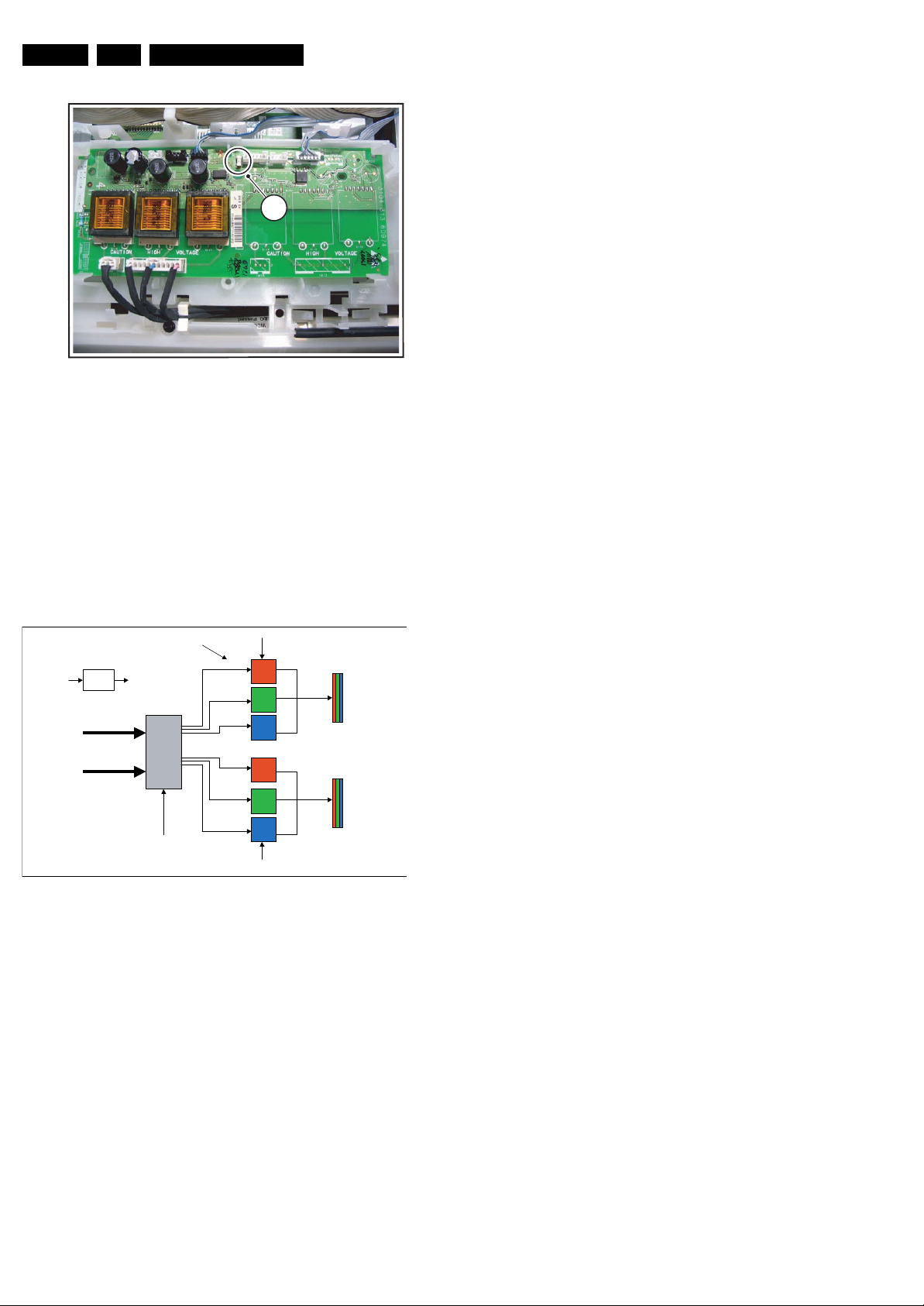
Figure 5-2 Service Mode pads AmbiLight panel
In this chassis, both single and double fitted boards can be
used. The double fitted boards are used in sets with 3 or 4
sided Ambi Light units whereas the single fitted boards are
used in sets with 2 sided Ambi Light units. A double fitted board
can drive 2 lamp units (6 lamps) and a single fitted board can
drive 1 lamp unit (3 lamps).
The double fitted boards are supplied by +12Va and +12Vb.
The microprocessor is supplied by +12Va.
Therefore, if only +12Va is available, lamp unit B will not work.
See figure “Building blocks of Converter Board” for details.
+12Va
Stab.
Board select
+5V
Inverters
µ
Processor
PWM out
+12Va
I²C
Protection
+12Vb (12
-13V)
060406
Lamp unit A
Lamp unit B
G_15950_050.eps
060406
In case the Ambi Light switches off after two seconds, serial
arcing or parallel arcing protection is active. Serial arcing
protection can be excluded by disconnecting the opto-coupler;
check for bad solder joints on transformer or lamp units.
Parallel arcing protection can be disabled by grounding pin 8 of
the microprocessor. Usually the switching frequency (normally
63 kHz) will then be too high. Possible causes are one
MOSFET of the converter has no gate drive or is broken, or
there is a short-circuit of the output of the transformer.
5.3 Stepwise Start-up
The stepwise start-up method, as known from FTL/FTP sets
(EMG based sets) is not valid any more. There are two possible
situation: one for protections detected by standby software and
one for protections detected by main software.
When the TV is in a protection state due to an error detected by
standby software (and thus blinking an error) and SDM is
activated via shortcutting the pins on the SSB, the TV starts up
until it reaches the situation just before protection. So, this is a
kind of automatic stepwise start-up. In combination with the
start-up diagrams below, you can see which supplies are
present at a certain moment. Important to know here is, that if
e.g. the 3V3 detection fails (and thus error 11 is blinking) and
the TV is restarted via SDM, the Stand-by Processor will
enable the 3V3, but will not go to protection now. The TV will
stay in this situation until it is reset (Mains/AC Power supply
interrupted).
When the TV is in protection state due to an error detected by
main software (Viper protection) and SDM is activated via
shortcutting the pins on the SSB, the TV starts up and ignores
the error. Due to architectural reasons it is possible that the TV
will end up in an undefined state (e.g. when the fast I
blocked). In this case diagnose has to be done via ComPair.
The abbreviations “SP” and “MP” in the figures stand for:
• SP: protection or error detected by the Stand-by
Processor.
• MP: protection or error detected by the VIPER Main
Processor.
In the next transition diagrams for “POD” should be read
“Common Interface (CI)”. For analogue sets, any reference to
“POD” should be neglected.
2
C bus is
Figure 5-3 Building blocks of Converter Board
The microprocessor performs the following tasks:
• Dimming of Ambi Light by means of PWM.
• Translation of I
2
C-bus commands to PWM.
• Switches the Ambi Light board to protection if needed (in
case of protection only the lamps switch off, no set
protection is triggered).
There are two ways of protection: parallel arcing protection and
serial arcing protection.
Parallel arcing protection is performed by sensing the switching
frequency. In case of short circuit of the transformer output, this
frequency > 100 kHz and the board goes into protection.
Serial arcing protection is performed by detection of arc in
ground wire of the lamp units. In this case, the protection pulse
is transmitted via an opto-coupler.
Protection can be disabled by short-circuiting diode 6112 or
capacitor 2173 or by connecting pin 8 of the microprocessor to
ground.
 Loading...