

Page 1

PSSG
PHILIPS SERVICE SOLUTIONS GROUP
PHILIPS TECHNICAL
TRAINING
PHILIPS
TECH
VIDEOTA PE S
MANUALS
COLOR TV
CHASSIS
Philips Technical Training (USA)
401 E. Old Andrew Johnson hwy
PO box 555
Jefferson City, TN 37760
PH: 865-475-0397
FAX: 865-475-0221
TRAINING
EMAIL: [email protected]
F8
Page 2

F8 COLOR TV CHASSIS INTRODUCTION.
The F8 chassis is a leader TV
chassis produced by Philips
Consumer Electronics Company for
the 1999 model year. (Figure 1)
The F8 is used in sets with 25, 27,
and 32 inch screen sizes. The F8
chassis is a global design and is
oriented front to rear, or "north
to south", as it has been called.
The F8 chassis tuning system
features 181 channels with onscreen display. The main tuning
system uses a tuner, a
microcomputer IC, and a memory IC
mounted on the main chassis. The
microcomputer communicates with the
memory IC, the customer keyboard,
remote receiver, U/V tuner, signal
processor IC and the audio output
IC via the I2C bus. The memory IC
retains the settings for favorite
stations, customer preferred
settings, and service/factory data.
The F8 chassis uses a Very Large
Scale (VLSI) Integrated Circuit for
signal processing. This IC performs
video IF, sound IF processing, AGC
control, horizontal and vertical
drive and synchronization, also
Luminance/Chrominance processing.
The on-screen graphics and closed
caption decoding are done within
the microprocessor, and then sent
to the signal processor IC to be
added to the main signal.
The F8 chassis utilizes a switch
mode power supply for the main
voltage source. The chassis has a
hot chassis ground reference on the
primary side of the power supply,
and a cold ground reference on the
secondary side of the power supply
and the rest of the chassis.
ALWAYS USE AN ISOLATION
TRANSFORMER WHEN SERVICING THIS
CHASSIS FOR YOUR SAFETY.
SIGNAL FLOW
The incoming RF signal is
applied to the U/V tuner where
the 45.75 MHz IF signal is
developed and amplified. The IF
signal then exits the tuner from
pin10 to pass through the SAW
filter. The shaped signal is
then applied to IC 7250, the IF
processor. The automatic gain
control (AGC) is performed in IC
7250 and applied to the U/V
tuner at pin 1. An automatic
fine tuning signal (AFT) is also
generated in the IC and then
routed to the tuning system via
the I2C bus, to provide
frequency correction as needed.
Composite Video is output on Pin
6 of 7250 and buffered by
transistor 7266. In Mono Audio
sets, the signal is applied to
1001, 4.5 MHz Band Pass Filter,
and then applied to Pin 1 and
the Audio Demodulator circuit.
Audio is then output on Pin 15
and applied to the Audio
Amplifier 7953. Volume level is
controlled at the Audio Output
IC by a control line from the
Microprocessor. The Audio from
7953 is then sent to the
Headphone Speaker output panel.
In Stereo sets, the signal is
amplified by transistor 7831 and
applied to Pin 58 of 7833,
Stereo Decoder. The switcher
inside the Stereo decoder IC
selects between the internal
decoder, FRONTAUDIO1, or
EXT2AUDIO. The output of the
PAGE 1
Page 3
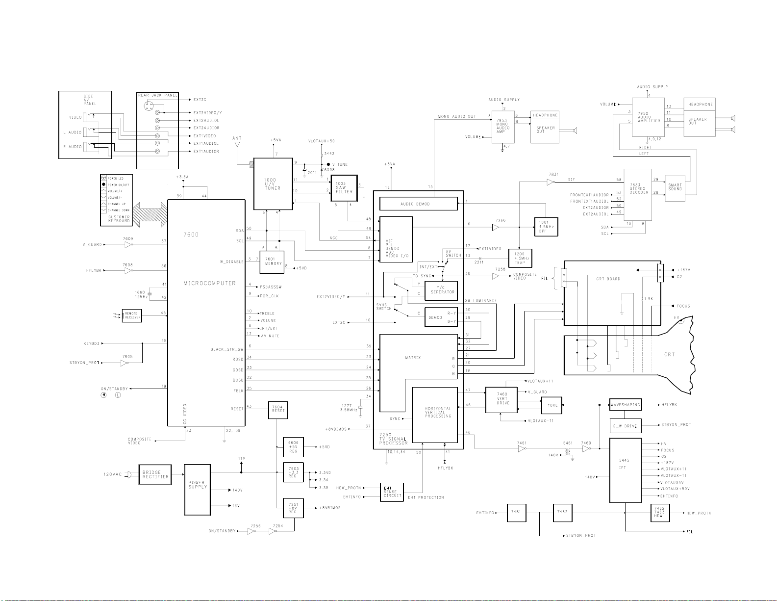
FIGURE 1 - BLOCK DIAGRAM
PAGE 2
Page 4

Stereo decoder is fed to the Smart
Sound circuit and then to 7950,
Audio Amplifier. The Volume level
is controlled by the
Microprocessor, via the Volume
line, at the Audio Amplifier IC.
Composite Video from 7266 is also
applied to the 4.5 MHz trap, 1200,
to remove the audio signal. The
signal is then applied to Pin 13 of
the IC. The Video switch in 7250
selects between Pin 13, EXT1VIDEO
on Pin 17, and EXT2VIDEO on Pin 11.
The selected signal is then applied
to the Y/C Separator. The output
of the YC separator is then fed to
the SVHS switch which selects
between the output of the YC
separator or external YC on Pins 11
and 10. The Y Signal from the YC
separator is output on Pin 28 and
is fed to the Matrix circuits on
Pin 27. R-Y and B-Y from the
Demodulator is output on Pins 30
and 29. This signal is then fed to
the Matrix circuit on Pins 32 and
31. OSD signal from the
Microprocessor is mixed with the
main signal in the Matrix before
being output to the CRT board on
Pins 19, 20, and 21.
Vertical and Horizontal drive
signals are also developed inside
IC 7250. Vertical drive exits the
IC from pin 47, while Horizontal
drive exits at pin 40. These
signals are a product of a Voltage
Controlled Oscillator Circuit (VCO)
and divider network located inside
the chip. Vertical drive is applied
to pin 1 of IC 740, amplified,
shaped, and output from pin 5 where
it is applied to the vertical
winding of the yoke. A feedback
signal is returned to pin 46 of IC
7250. The Vertical sync pulse is
also applied to the
microprocessor, IC 7600, to pin
37 for On-Screen Display and
Closed-Captioning
synchronization. The Horizontal
drive signal exits IC 7250 from
pin 40 and is applied to 7461,
the Horizontal Driver transistor.
The signal is amplified and
coupled to the base circuit of
7460, the Horizontal Output
transistor. The H.O.T. drives the
Integrated Flyback Transformer,
which provides high voltage,
screen voltage, focus, G-2, and
filament voltages for the CRT. A
scan-derived power supply is also
provided by the IFT. It supplies
-11 volts, +11 volts, +50 volts,
a secondary +5 volt supply, and
a +187 volt source for video
drive. The secondary of the IFT
is monitored by the HEW_PROTN
and EHT_INFO lines. These lines
are fed to the Signal Processor,
7250. This circuit will shut
the Horizontal drive Off in case
of Overvoltage or excessive Beam
Current. Transistor 7482 also
monitors the Filament line for
Overvoltage. Transistor 7481
monitors the EHTINFO or DAG line
of Overcurrent. The E_W drive
circuit also monitors for the
loss of Horizontal output. If
any one of these three circuits
detect a failure, a High will
be placed on the STBYON_PROT
line. This will turn transistor
7605 On causing Pin 16 of 7600
to go Low. The Microcomputer
will then turn the set Off.
The Power Supply in the set is
On any time power is applied to
the set. The Power Supply
produces a 140, 16, and 11 volt
supplies. The 11 volt supply is
PAGE 3
Page 5
applied to 7603 to produce the 3.3
volt supply for the Microcomputer
and to 6606 to produce the +5VD
supply. When the set is turned On,
the On/Standby line goes High
turning transistor 7256 On, turning
transistor 7254 Off, which turns
the 8 volt regulator, 7251, On.
This supply is applied to Pin 37 of
7250, the Signal Processor IC, to
power the Horizontal and Vertical
Oscillator. The Horizontal output
drives the Horizontal Output
section to produce the Scan derived
sources.
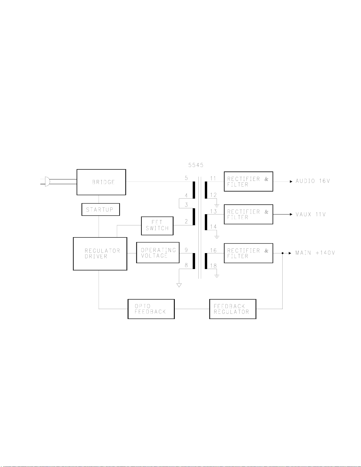
POWER SUPPLY
When a 120Vac Source is
connected to the F8 Chassis
(Figure 2), approximately 160Vdc
is developed by the Bridge
Rectifier circuit. The 160 volts
dc goes through the primary of
transformer 5545 to the FET
switch. The startup voltage for
the IC is taken from the hot leg
of the input ac. Operating
voltage for the driver circuit
is taken from the HOT side of
5545, Pin 9.
FIGURE 2 - POWER SUPPLY BLOCK
The Power Supply is a Switching
Mode type Power Supply. The
frequency of operation varies with
the circuit load. There is no
separate power supply for standby;
instead, the Power Supply starts
operating when AC is applied. The
Switching Regulator IC starts
switching when the initial voltage
is applied through the Startup
circuit. The Switching Regulator
turns the Switch On and Off to
control current flow through the
primary of transformer 5545.
Energy stored in the primary
during the On-time is delivered
to the secondaries during the
Off-time. Feedback from the 140
volt supply is used to control
PAGE 4
Page 6
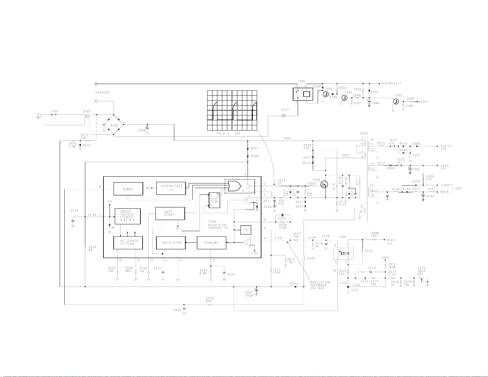
FIGURE 3 - POWER SUPPLY DIAGRAM
PAGE 5
Page 7

the Switching Regulator via the
Optoisolator feedback.
From the secondaries of 5545, 16
volts is developed for the audio
circuit, 140 volts
for the Horizontal Output, and 11
volts for the Horizontal
Oscillator, 3.3 volt, and 5 volt
regulators.
STARTUP (FIGURE 3)
AC voltage is rectified by the
bridge 6505 to produce
approximately 160 volts dc. The
160 volts dc is applied to primary
winding of 5545 and to the Drain
of the switching regulator FET
7518.
A startup dc voltage ramp is
developed when the Hot side of the
ac line charges capacitor 2540
through Startup resistors 3510 and
3530. When the voltage at capacitor
2540 and Pin 1 of 7520 IC reaches
14.5 volts, the under-voltage lockout of the IC is overcome.
The Oscillator inside the IC turns
on driving the Flip Flop producing
a 10 volt peak to peak drive pulse
at Pin 3, turning On transistor
7518. The drive voltage for the
output at Pin 3 is supplied to the
IC at Pin 2. Energy is stored in
transformer 5545 during the On-time
of transistor 7518. During the Off
time of transistor 7518, energy is
transferred to the secondaries.
Since resistors 3510 and 3530
cannot supply sufficient current to
operate the IC in normal operation,
the voltage at Pin 1 of IC 7520
drops below 9.4 volts, which is
below the under voltage lockout
reference, shutting IC 7520 Off.
2540 again charges to 14.5 volts
through resistors 3510 and 3530
turning the IC On for a second
time. Voltage from Hot
secondary Pin 9 of transformer
5545 is rectified by diode 6540,
charging capacitor 2540 during
each startup cycle. Once 5545
stores enough energy to keep
capacitor 2540 above 9.4 volts,
the IC operates normally.
Capacitor 2530 is connected to
the Soft Start circuit preventing
the IC from operating until the
supplies inside the IC have
reached the correct operating
voltage.
STANDBY (Figure 3)
The 140 volt supply is the
reference supply for the power
supply. The 140 volt supply is
sampled by resistors 3571 and
fed to the input of the Shunt
Regulator 7570. Variable
resistor 3572 is used to set the
140 volt supply to the correct
level. The Shunt Regulator
drives the feedback optoisolator
7581 to set the feedback control
voltage on Pin 14 of 7520.
Voltage from the Feedback circuit
is monitored by Pin 14 of the IC
and is compared to a 2.5 volt
reference for feedback sensing.
When the set is turned Off, the
reduced load on the secondary is
felt by Pin 14 of IC 7520. This
voltage change on Pin 14 is too
small for a voltmeter to
measure; therefore, the output of
the comparator should be
measured at Pin 13. The voltage
will be approximately 1.7 volts
in Standby and 2.7 volts in the
Full Power Mode. The Standby
Circuit inside the IC monitors
PAGE 6
Page 8

the output of the feedback
comparator, switching the
Oscillator to 20KHz in the
Standby Mode and 38KHz in the Full
Power Mode. In the Standby Mode,
the pulse width at Pin 3 of 7520 IC
is reduced, which reduces the On
time of transistor 7518.
FULL POWER
The IC's internal comparator,
connected to Pin 14, senses a load
change when the set is turned On.
The Standby circuit switches the
output to 38 KHz and increases the
output's pulse width. The Demag
circuit at Pin 8 of the IC monitors
Pin 9 of 5545 through resistor
3520. This circuit keeps Pin 3 of
the IC from going High until Pin 1
reaches 0 volts. This is to ensure
that FET 7518 will not turn on
until demagnetization of
transformer 5545 is complete. The
purpose of this circuit is to
increase the efficiency of the
power supply. Pin 7 of the IC
senses the voltage across resistor
3518 caused by current flow through
transistor 7518. If this voltage
exceeds 1 volt, the pulse width at
Pin 3 of the IC, or the On time of
7518, will be reduced, turning 7518
Off sooner. The internal
Overvoltage circuit of 7520 IC
monitors the VCC at Pin 1 of the
IC. If this voltage goes above 17
volts, the Power Supply will shut
down. AC power will have to be
removed before the Power Supply
will Restart when this occurs.
TROUBLESHOOTING
In the case of a Dead Set, first
check the startup voltage at Pin 1
of IC 7520. If this voltage is
missing, check for an open fuse
1500, a shorted IC 7520, a
shorted diode in the Bridge, or
open resistors 3510 and 3530.
If there is no output voltage
from the supply, the voltage at
Pin 1 of IC 7520 should be
changing. This voltage must go
to 14.5 volts to overcome the
undervoltage lockout of the IC.
If the IC is working, a series
of drive pulses can be seen with
an oscilloscope at Pin 3 of the
IC at approximately one to two
second intervals. Unless the
undervoltage lockout is switched,
the Reference Section will not
turn On to power the Oscillator
and drive section in the IC.
If the voltage is changing at
Pin 3 of IC 7520, check the FET
7518 and surrounding components.
Symptoms
For a no Power or Dead Set
condition, first check for
shorts on the output
secondaries. Check B+ voltages
at Pin 5 of transformer 5545. A
short on the 140 volt B+ line
will cause Pin 1 of IC 7520 to
pulse between approximately 9
and 15 volts. The feedback
voltage at Pin 14 will go to
zero volts. A random series of
drive pulses will be generated
at Pin 3.
If the Output drive circuit,
transistor 7518 is lost, such as
an open resistor 2525 and IC
7520 is working, the voltage at
Pin 1 of 7520 will pulse between
9 and 15 volts. A series of
output pulses will appear at Pin
PAGE 7
Page 9
3 of IC 7520 each time Pin 1 goes
to 14.5 volts.
If 2530 should become leaky or
shorted causing Pin 11 of IC 7520
to go Low, the IC will not Start.
Capacitor 2530 provides a delay for
the Soft Start circuit. If Pin 11
is held Low, the output of the Soft
Start circuit will remain High.
If 7518 should fail, resistor 3518,
which is connected to the source of
7518, should be replaced as part of
any repair. Resistor 3518 is
the current sensing resistor for
transistor 7518. If 3518 should
increase in value, Comparator B
would turn on too soon. This
would reset the flip-flop too
soon. Transistor 7518 would not
remain on long enough to store
sufficient energy in the
transformer to operate the set.
Resistor 3518 is a precision
resistor and should only be
replaced with the correct part
number.
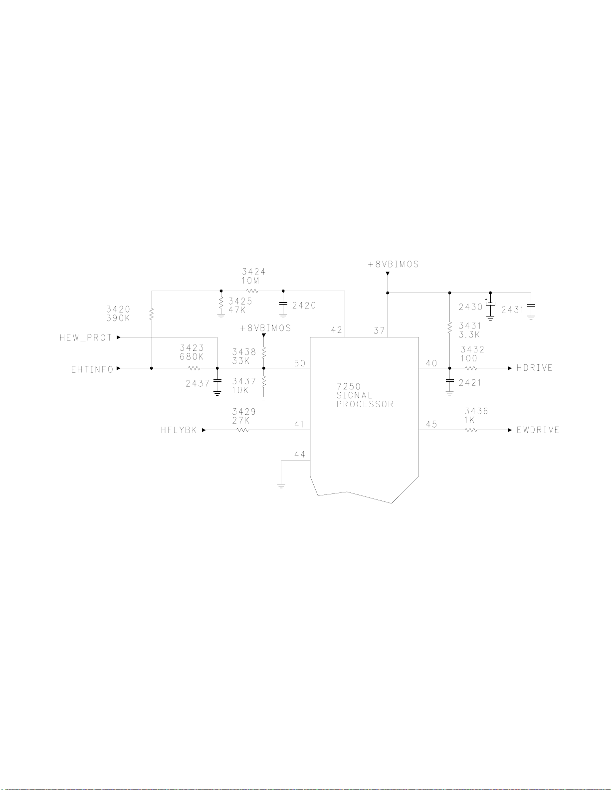
FIGURE 4 - HORIZONTAL DRIVE CIRCUIT
F8 HORIZONTAL DRIVE CIRCUIT
(Figure 4)
When the set is turned On, the
+8VBIMOS voltage is applied to Pin
37 of 7250. Horizontal drive is
then output on Pin 40 of the IC.
HFLYBK is fed to Pin 41 to phase
lock the Horizontal oscillator.
Drive for the E_W circuit is output
on Pin 45. If the HEW_PROT or
EHTINFO lines should go High, the
Horizontal drive on Pin 40 will
be shut Off.
F8 HORIZONTAL OUTPUT CIRCUIT
(Figure 5)
Horizontal drive is applied to
7461 and to 7460 to drive the
IFT, 5445. The secondary of
5545 produces High voltage, Focus
voltage, G2 voltage, +11 volts,
-11 volts, +50 volts, Filament
PAGE 8
Page 10
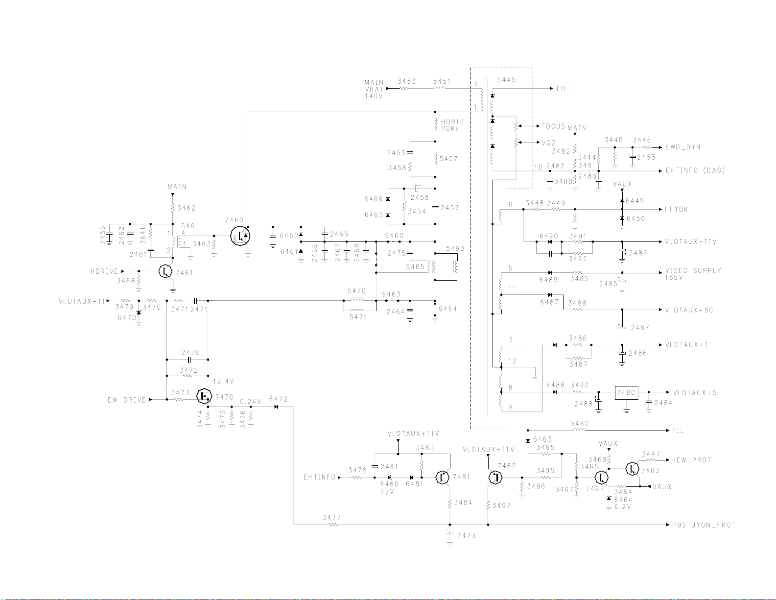
FIGURE 5 - HORIZONTAL OUTPUT CIRCUIT
PAGE 9
Page 11
voltage, and +5 volts. The EHTINFO
line is the DAG line. This line is
fed back to the Signal Processor
IC, 7250, to adjust the Picture
level to compensate for changes in
Beam Current. The EHTINFO line is
also connected to resistor 3478 and
zener diode 6480. If this line
should go excessively negative,
which would be caused by excessive
Beam Current, transistor 7481 will
turn On. This will place a High on
the P9STBYON_PROT line shutting the
set Off. The Filament voltage is
monitored for no voltage or
excessive voltage. The Filament
voltage is rectified by 6463 and
fed to the base of transistor 7462.
If the voltage on the base of 7462
goes above 6.8 volts, 7462 will
turn On, turning 7463 On. This
will place a High on the
HEW_PROT line. This will shut
the Horizontal drive Off. The
EW_DRIVE from the Signal
Processor drives transistor 7470
to make linearity corrections in
the Horizontal Drive. If
Horizontal drive should fail, the
source leg of 7470 will go High,
placing a High on the
P9STBYON_PROT line shutting the
set down.
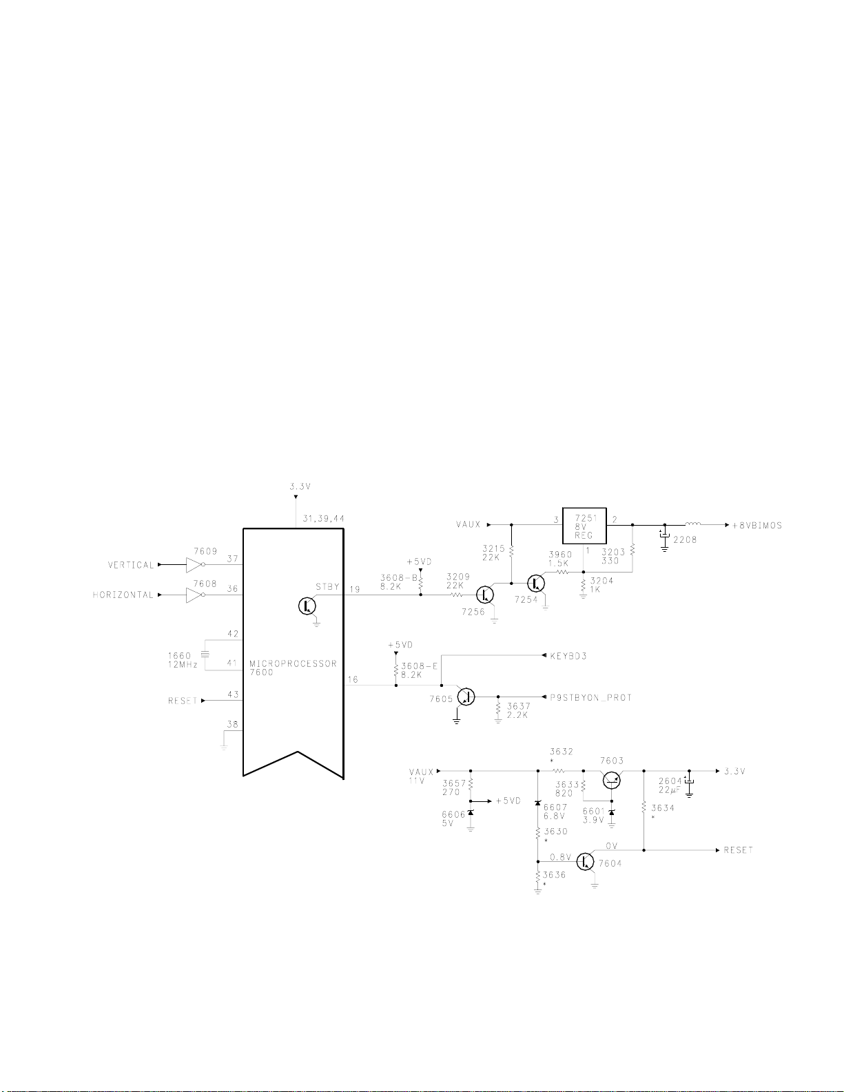
MICROPROCESSOR SWITCHING (Figure
6)
In the Standby mode, Pin 19 of
the Microprocessor, 7600, is held
Low by a switching circuit
inside the IC. When Set is
turned On, this circuit switches
FIGURE 6 - MICROPROCESSOR
PAGE 10
Page 12

Off. Transistor 7256 then turns On
through 3608-B. Transistor 7254
then turns Off. The 8 volt
regulator 7251 then turns On
placing 8 volts on the +8VBIMOS
line. This source provides power
to the Horizontal oscillator
section of the Signal Processor IC.
If the P9STBYON_PROT line should
go High, transistor 7605 will
turn On. This will pull Pin 16
of 7600 Low, shutting the set
Off.
PAGE 11
Page 13

DOES THE SET
TURN ON
START
DOES THE SET SHUT
DOWN AFTER BEING
TURNED ON
DOES THE SET
HAVE A PICTURE
IS AUDIO
PRESENT
IS 140V VBAT PRESENT ON
THE CATHODE OF 6550
NO
YES NO YES
IS THE
RESISTANCE
> 4K
IS 140-160 VOLTS
PRESENT ON THE
DRAIN OF 7518
NO
YES
MEASURE THE
RESISTANCE FROM
THE CATHODE OF
6550 TO COLD
GROUND
CHECK FUSE 1500
BRIDGE 6505
NO
CHECK 7460 HOT
NO
IS DRIVE SIGNAL
PRESENT ON PIN 3
OF 7520
NO
IS VOLTAGE ON PIN 1 OF
7520 CHANGING BETWEEN
9.4 AND 14.5 VOLTS
IS > 15 VOLTS
PRESENT ON PIN 1
OF 7520
CHANGE 7520
CHECK RESISTORS
3530, 3510
DIODE 6510
BRIDGE 6505
NO NO NO
YES YES
IS DRIVE SIGNAL
PRESENT ON THE
DRAIN OF 7518
RESISTOR 3525
DIODE 6514
TRANSISTOR 7518
REGULATION
FEEDBACK CIRCUIT
7581
11 VOLT SOURCE
YES
NO
YES
IS 8V DC PRESENT
ON PIN 2 OF 7251
IS HORIZ DRIVE
PRESENT ON PIN
40 OF 7250
IS HORIZ DRIVE
PRESENT ON THE
BASE OF 7460
DOES PIN 19 OF 7600
GO HIGH WHEN THE
POWER BUTTON IS
PRESSED
IC 7250
TRANSISTOR 7460
RESISTOR 3608
IC 7600
3.3 VOLT SOURCE
TRANSISTORS 7256 &
7254
YES YES YES YES
NO
NO
YES
NO
CHECK 7461
TRANSFORMER 5461
NO
YOUR PROBLEM IS
BEYOND THE SCOPE
OF THIS FLOW CHART
B
YES
NO
A
NO
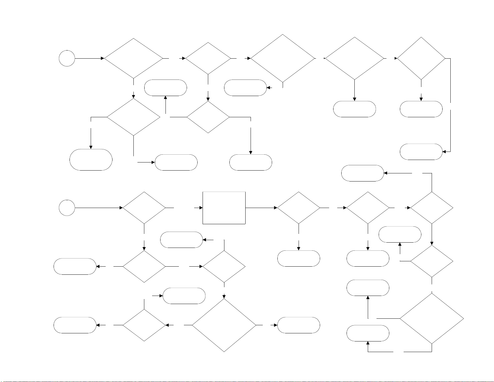
F8 TROUBLESHOOTING
FLOW CHART
C
NO
PAGE 12
Page 14
A
DOES PIN 16 OF 7600 GO
LOW AFTER THE SET IS
TURNED ON
IS > 3.9 VOLTS
PRESENT ON PIN 50 OF
7250 WHEN THE SET IS
TURNED ON
MICRO 7600
I2C BUS
TRANSISTOR 7462 &
7463
IFT
TUNING CAPS
IS THE EHTINFO
LINE
< -28 VOLTS
IS 186 VOLT
SUPPLY PRESENT
TO THE CRT
BOARD
RESISTOR 3485
DIODE 6485
CRT BOARD
NO
YES
YES
NO
YES
NO
YES
DOES THE COLLECTOR OF
7482 GO TO 11 VOLTS WHEN
THE SET IS TURNED ON
DOES THE COLLECTOR
OF 7481 GO TO 11 VOLTS
WHEN THE SET IS
TURNED ON
DOES THE SOURCE
OF 7470 GO HIGH
WHEN THE SET IS
TURNED ON
NO NO NO
TRANSISTOR 7482
FILAMENT VOLTAGE
7481
DIODE 6480
7605
7470
YES
YES
NO
B
IS THE SET
STEREO OR MONO
IS AUDIO
PRESENT
STEREO
INSERT AUDIO INTO
THE REAR JACK
PANEL AND SELECT
THAT INPUT
IS AUDIO
PRESENT ON PINS
28 & 29 OF 7833
IS AUDIO
PRESENT ON PINS
8,10,11,&13 OF
7950
NO YES
TRANSISTOR 7831
IC 7833
YES
IC 7833
NO
CHECK HEADPHONE
SWITCH
SPEAKERS
YES
IS 16V PRESENT
ON PIN 4 OF 7950
FUSE 1573
NO
YES
IS THE DC VOLTAGE ON PINS
2 & 8 OV 7950 BETWEEN 0-1
VOLTS AS THE VOLUME IS
ADJUSTED
IC 7600
ANTI-POP CIRCUIT
IC 7950
YES
NO
IS AUDIO
PRESENT ON PIN 3
OF 7953
MONO
IC 7250
1001 4.5 BPF
IS AUDIO
PRESENT ON PINS
6 & 8 OF 7953
DOES THE VOLTAGE ON PIN
5 OF 7953 VARY BETWEEN 0-
1 VOLTS AS TEH VOLUME IS
ADJUSTED
IS 16 VOLTS DC
PRESENT ON PIN 2
OF 7953
YES
NO
YES
CHECK HEADPHONE
JACKS AND
SPEAKERS
YES
IC 7953
FUSE 1573
MICRO 7600
ANTI POP CIRCUIT
NO
NO NO
YES
PAGE 13
Page 15

C
IS OSD (ON
SCREEN DISPLAY)
PRESENT
IS RGB PRESENT ON
PINS 21, 20, AND 19 OF
7250
NO
7250
CRT BOARD
DOES THE SET
HAVE A JACK
PANEL
YES
INSERT A COMPOSITE
VIDEO SIGNAL INTO
EXT1 AND SELECT
THAT INPUT IN THE
MENU
YES
IS VIDEO PRESENT
ON SCREEN
SELECT THE TUNER IN
THE MENU AND
CHECK FOR
COMPOSITE VIDEO ON
PIN 6 OF 7250
NO YES
IS VIDEO PRESENT
ON PIN 6
IS LUMINANCE
PRESENT ON PIN
28 OF 7250
7250
NO
YES
IS VIDEO PRESENT ON
PIN 13 OF 7250
YES
TRANSISTOR 7266
1200 4.5MHz TRAP
NO
IS LUMINANCE
PRESENT ON PIN
27 OF 7250
YES
CHECK CIRCUIT
BOARD CONNECTIONS
7250
NO
YES
IS 5V SUPPLY PRESENT
ON PIN 7 OF THE
TUNER
CHECK RESISTOR
3490, 7480 IC, IFT
NO
NO
IS 33V PRESENT
ON PIN 9 OF THE
TUNER
YES
CHECK RESISTOR
3442, DIODE 6008,
TUNER, RESISTOR
3488, IFT
NO
DISCONNECT PINS 10
& 11 OF THE TUNER
AND APPLY AN IF
SIGNAL TO THE
CIRCUIT FOIL
YES
IS THE PICTURE
PRESENT ON THE
SET
TUNER
YES
INSERT AN IF SIGNAL
ON PINS 48 AND 49 OF
7250
NO
IS PICTURE
PRESENT ON THE
SET
7250
1003 SAW FILTER
NO
YES
PAGE 14
 Loading...