

Philips f40 DATASHEETS
Philips Semiconductors FAST Products Product specification
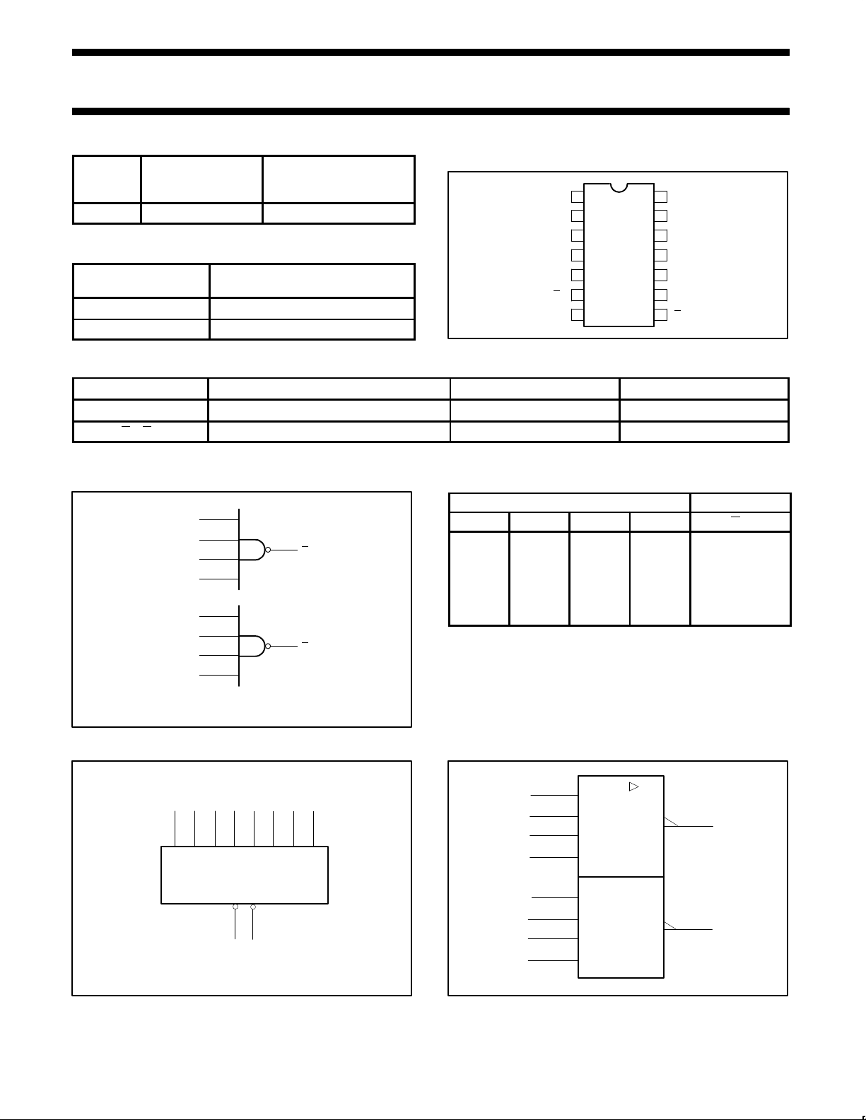
74F40Dual 4-input NAND buffer
1
April 11, 1989 853–0053 96314
TYPE
TYPICAL
PROPAGATION
DELAY
TYPICAL
SUPPLY CURRENT
(TOTAL)
74F40 3.5ns 6mA
ORDERING INFORMATION
DESCRIPTION
COMMERCIAL RANGE
V
CC
= 5V ±10%, T
amb
= 0°C to +70°C
14-pin plastic DIP N74F40N
14-pin plastic SO N74F40D
PIN CONFIGURATION
14
13
12
11
10
9
87
6
5
4
3
2
1
GND
V
CC
D1b
D1a
Q1
NC
D1d
D1c
D0a
D0b
Q
0
NC
D0c
D0d
SF00065
INPUT AND OUTPUT LOADING AND FAN OUT TABLE
PINS DESCRIPTION 74F (U.L.) HIGH/LOW LOAD VALUE HIGH/LOW
Dna, Dnb, Dnc, Dnd Data inputs 1.0/2.0 20µA/1.2mA
Q0, Q1 Data outputs 750/106.7 15mA/64mA
NOTE: One (1.0) FAST unit load is defined as: 20µA in the High state and 0.6mA in the Low state.
LOGIC DIAGRAM
VCC = Pin 14
GND = Pin 7
NC = Pin 3, 11
SF00081
Q0
6
1
2
4
D0a
D0b
D0c
5
D0d
Q1
8
9
10
12
D1a
D1b
D1c
13
D1d
FUNCTION TABLE
INPUTS OUTPUT
Dna Dnb Dnc Dnd Qn
L X X X H
X L X X H
X X L X H
X X X X H
H H H H L
NOTES:
1. H = High voltage level
2. L = Low voltage level
3. X = Don’t care
LOGIC SYMBOL
D1a D1bD0a D0b D0c D1c D1dD0d
Q0 Q1
6 8
1 2 4 5 9 10 12 13
VCC = Pin 14
GND = Pin 7
NC = Pin 3, 11
SF00082
IEC/IEEE SYMBOL
SF00083
&
6
8
1
2
4
5
9
10
12
13
Philips Semiconductors FAST Products Product specification
74F40Dual 4-input NAND buffer
April 11, 1989
2
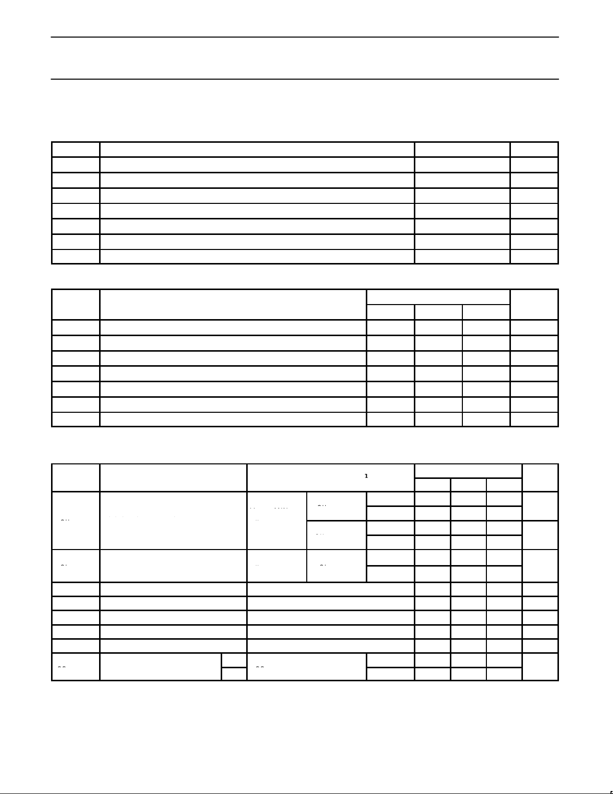
ABSOLUTE MAXIMUM RATINGS
(Operation beyond the limits set forth in this table may impair the useful life of the device.
Unless otherwise noted these limits are over the operating free-air temperature range.)
SYMBOL
PARAMETER RATING UNIT
V
CC
–0.5 to +7.0 V
V
IN
Input voltage –0.5 to +7.0 V
I
IN
–30 to +5 mA
V
OUT
Voltage applied to output in High output state –0.5 to V
CC
V
I
OUT
Current applied to output in Low output state 128 mA
T
amb
Operating free-air temperature range 0 to +70 °C
T
stg
Storage temperature range –65 to +150 °C
RECOMMENDED OPERATING CONDITIONS
LIMITS
SYMBOL
PARAMETER
MIN NOM MAX
UNIT
V
CC
Supply voltage 4.5 5.0 5.5 V
V
IH
High-level input voltage 2.0 V
V
IL
Low-level input voltage 0.8 V
I
IK
Input clamp current –18 mA
I
OH
High-level output current –15 mA
I
OL
Low-level output current 64 mA
T
amb
Operating free-air temperature range 0 +70 °C
DC ELECTRICAL CHARACTERISTICS
(Over recommended operating free-air temperature range unless otherwise noted.)
LIMITS
SYMBOL
PARAMETER
TEST CONDITIONS
1
MIN TYP
2
MAX
UNIT
±10%V
CC
2.5
IOH = –1mA
±5%V
CC
2.7 3.4
V
VOHHigh-level output voltage
VIL = MAX,
VIH = MIN
±10%V
CC
2.0
VIH = MIN
IOH = –15mA
±5%V
CC
2.0
V
±10%V
CC
0.55
VOLLow-level output voltage
VIL = MAX,
V
IH
= MIN
IOL = MAX
±5%V
CC
0.42 0.55
V
V
IK
Input clamp voltage VCC = MIN, II = I
IK
–0.73 –1.2 V
I
I
Input current at maximum input voltage VCC = MAX, VI = 7.0V 100 µA
I
IH
High-level input current VCC = MAX, VI = 2.7V 20 µA
I
IL
Low-level input current VCC = MAX, VI = 0.5V –0.6 mA
I
OS
Short-circuit output current
3
VCC = MAX –100 –225 mA
I
CCH
VIN = GND 1.75 4.0
ICCSupply current (total)
I
CCL
VCC = MAX
VIN = 4.5V 11 17
mA
NOTES:
1. For conditions shown as MIN or MAX, use the appropriate value specified under recommended operating conditions for the applicable type.
2. All typical values are at V
CC
= 5V, T
amb
= 25°C.
3. Not more than one output should be shorted at a time. For testing I
OS
, the use of high-speed test apparatus and/or sample-and-hold
techniques are preferable in order to minimize internal heating and more accurately reflect operational values. Otherwise, prolonged shorting
of a High output may raise the chip temperature well above normal and thereby cause invalid readings in other parameter tests. In any
sequence of parameter tests, I
OS
tests should be performed last.
Supply voltage
Input current
VCC = MIN,
VCC = MIN,
 Loading...