

Page 1

®
PRODUCT SPECIFICATIONS
Integrated Circuits Group
LH28F160S5T-L70A
Flash Memory
16M (2M × 8/1M × 16)
(Model No.: LHF16K55)
Spec No.: EL104104
Issue Date: April 17, 1998
Page 2

SHARP
LHF16K55
l Handle this document carefully for it contains material protected by international copyright
law. Any reproduction, full or in part, of this material is prohibited without the express
written permission of the company.
l When using the products covered herein, please observe the conditions written herein
and the precautions outlined in the following paragraphs. In no event shall the company
be liable for any damages resulting from failure to strictly adhere to these conditions and
precautions.
(1) The products covered herein are designed and manufactured for the following
application areas. When using the products covered herein for the equipment listed
in Paragraph (2), even for the following application -areas, be sure to observe the
precautions given in Paragraph (2). Never use the products for the equipment listed
in Paragraph (3).
*Office electronics
alnstrumentation and measuring equipment
*Machine tools
*Audiovisual equipment
*Home appliance
&ommunication equipment other than for trunk lines
(2) Those contemplating using the products covered herein for the following equipment
which demands high reliability, should first contact a sales representative of the
company and then accept responsibility for incorporating into the design fail-safe
operation, redundancy, and other appropriate measures for ensuring &liability and
safety of the equipment and the overall system.
*Control and safety devices for airplanes, trains, automobiles, and other
transportation equipment
*Mainframe computers
l Traff ic control systems
*Gas leak detectors and automatic cutoff devices
*Rescue and security equipment
*Other safety devices and safety equipment, etc.
(3) Do not use the products covered herein for the following equipment which demands
extremely high performance in terms of functionality, reliability, or accuracy.
*Aerospace equipment
@Communications equipment for trunk lines
*Control equipment for the nuclear power industry
*Medical equipment related to life support, etc.
(4) Please direct all queries and comments regarding the interpretation of the above
three Paragraphs to a sales representative of the company.
.
l Please direct all queries regarding the products covered herein to a sales representative
of the company.
‘.
Rev.1.8
Page 3
SHARI=
LHFl6K55
CONTENTS
PAGE PAGE
1 INTRODUCTION ......................................................
1 .l Product Overview.. .............................................. 3
2 PRINCIPLES OF OPERATION.. ..............................
2.1 Data Protection ...................................................
3 BUS OPERATION ....................................................
3.1 Read ................................................................... 7
3.2 Output Disable ....................................................
3.3 Standby ............................................................... 7
3.4 Deep Power-Down .............................................. 7
3.5 Read identifier Codes Operation..
3.6 Query Operation.. ................................................
3.7 Write ....................................................................
3 COMMAND DEFINITIONS ....................................... 8
4.1 Read Array Command.. .....................................
4.2 Read Identifier Codes Command.. .................... 11
4.3 Read Status Register Command.. ..................... 11
4.4 Clear Status Register Command.. ..................... 11
4.5 Query Command.. ............................................. 12
4.51 Block Status Register .................................. 12
4.5.2 CFI Query Identification String.. ................... 13
4.5.3 System interface Information ....................... 13
4.5.4 Device Geometry Deffnition ......................... 14
4.5.5 SCS OEM Specific Extended Query Table . . 14
4.6 Block Erase Command ......................................
4.7 Full Chip Erase Command.. .............................. 15
4.8 Word/Byte Write Command.. ............................. 16
4.9 Multi Word/Byte Write Command.. .................... 16
4.10 Block Erase Suspend Command.. ................... 17
4.11 (Multi) Word/Byte Write Suspend Command
4.12 Set Block Lock-Bit Command..
4.13 Clear Block Lock-Bits Command.. ...................
4.14 STS Configuration Command ......................... 19
....................... 8
1 1
15
... 17
........................ 18
18
5 DESIGN CONSIDERATIONS
3
5.1 Three-Line Output Control ................................ .3C
5.2 STS and Block Erase, Full Chip Erase, (Multi)
6
7
7
7
8
8
Word/Byte Write and Block Lock-Bit Configuration
Polling.. ............................................................. .3C
5.3 Power Supply Decoupling.. ................................ 3C
5.4 V,, Trace on Printed Circuit Boards..
5.5 V,,, V,,, RP# Transitions..
5.6 Power-Up/Down Protection..
5.7 Power Dissipation
6 ELECTRICAL SPECIFICATIONS.. ........................ .3i
6.1 Absolute Maximum Ratings ............................... 32
6.2 Operating Conditions ......................................... 32
6.2.1 Capacitance .................................................
6.2.2 AC Input/Output Test Conditions..
6.2.3 DC Characteristics.. ..................................... .34
6.2.4 AC Characteristics - Read-&ly Operations .36
6.2.5 AC Characteristics - Write Operations..
6.2.6 Alternative CE#-Controlled
6.2.7 Reset Operations ......................................... 43
6.2.8 Block Erase, Full Chip Erase, (Multi)
Word/Byte Write and Block Lock-Bit
Configuration Performance.. ......................... 44
7 ADDITIONAL INFORMATION ....................... . ....... .45
7.1 Ordering Information
8 PACKAGE AND PACKING SPECIFICATION;;......4 6
............................................. .31
................................ .3C
............... .3C
..............................
.............................
...............
Writes.. ............. .41
................................ .I ........ 45
.......
1
.31
.31
32
.3C
.3S
Rev. 1.8
Page 4
SHARI=
16-MBIT (2MBx8/1 MBxl6)
Smart 5 Flash MEMORY
n
Smart 5 Technology
- 5V vcc
- 5V vpp
n
Common Flash Interface (CFI)
-
Universal & Upgradable Interface
n
Scalable Command Set (SCS)
n
High Speed Write Performance
-
32 Bytes x 2 plane Page Buffer
-
2ys/Byte Write Transfer Rate
n
High Speed Read Performance
- 70ns(5V=0.25V), 80ns(5VT0.5V)
LHFl6K55
LH28F160S5T-L70A
n
Enhanced Data Protection Features
-
Absolute Protection with Vpp=GND
-
Flexible Block Locking
-
Erase/Write Lockout during Power
Transitions
n
Extended Cycling Capability
-
100,000 Block Erase Cycles
-
3.2 Million Block Erase Cycles/Chip
n
Low Power Management
-
Deep Power-Down Mode
-
Automatic Power Savings Mode
Decreases ICC in Static Mode
2
n
n
Enhanced Automated Suspend Options
-
Write Suspend to Read
-
Block Erase Suspend to Write
-
Block Erase Suspend to Read
n
High-Density Symmetrically-Blocked
Architecture
-
Thirty-two 64-Kbyte Erasable Blocks
n
SRAM-Compatible Write Interface
n
User-Configurable x8 or x16 Operation
SHARP’s LH28F160S5T-L70A Flash memory with Smart 5 technology is a high-density, low-cost, nonvolatile,
read/write storage solution for a wide range of applications. Its symmetrically-blocked architecture, flexible voltage
and extended cycling provide for highly flexible component suitable for resident flash arrays, SlMMs and memory
cards. Its enhanced suspend capabilities provide for an ideal solution for code + data storage applications. For
secure code storage applications, such as networking, where code is either directly executed out of flash or
downloaded to DRAM, the LH28F160S5T-L70A offers three levels of protection: absolute protection with V,, at
GND, selective hardware block locking, or flexible software block locking. These alternatives give designers
ultimate control of their code security needs.
The LH28F160SST-L70A is conformed to the flash Scalable Command Set (SCS) and the Common Flash Interface
(CFI) specification which enable universal and upgradable interface, enable the highest system/device data transfer
rates and minimize device and system-level implementation costs.
Automated Write and Erase
-
Command User Interface
- Status Register
n
Industry-Standard Packa;ing
- 56-Lead TSOP
n
ETOXTM’ V Nonvolatile Flash
Technology
n
Not designed or rated as radiation
hardened
The LH28F160S5T-L70A is manufactured on SHARP’s 0.4pm ETOX
standard package: the 56-Lead TSOP, ideal for
‘ETOX is a trademark of Intel Corporation.
board constrained applications.
TM* V process technology. It come in industry-
%\
Rev. 1.8
Page 5
SHARP
LHFI 6K55
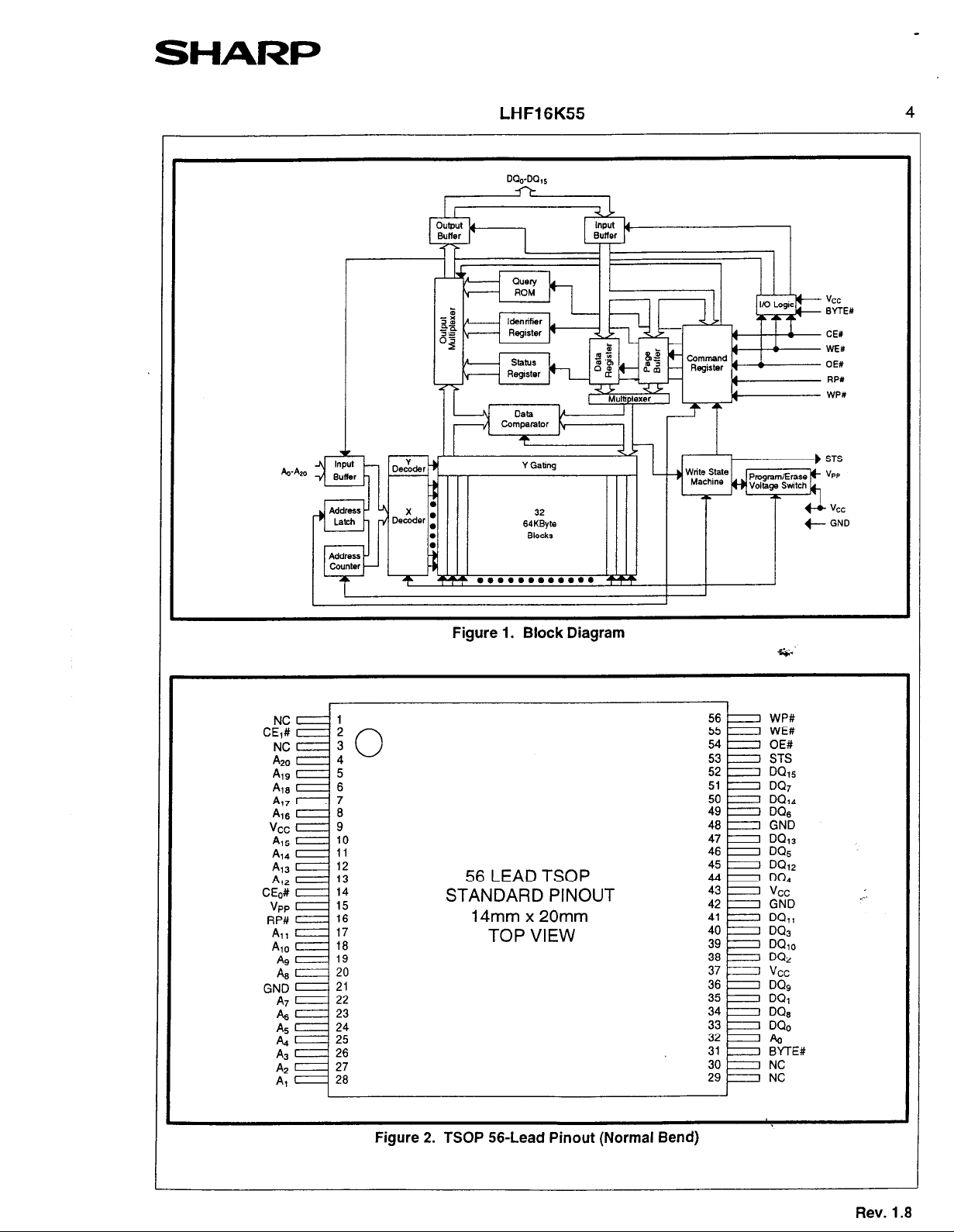
1 INTRODUCTION
This
specifications. Section 1 provides a flash memory
overview. Sections 2, 3, 4, and 5 describe the
memory organization and functionality. Section 6
covers electrical specifications.
datasheet contains
LH28F160.%T-L70A
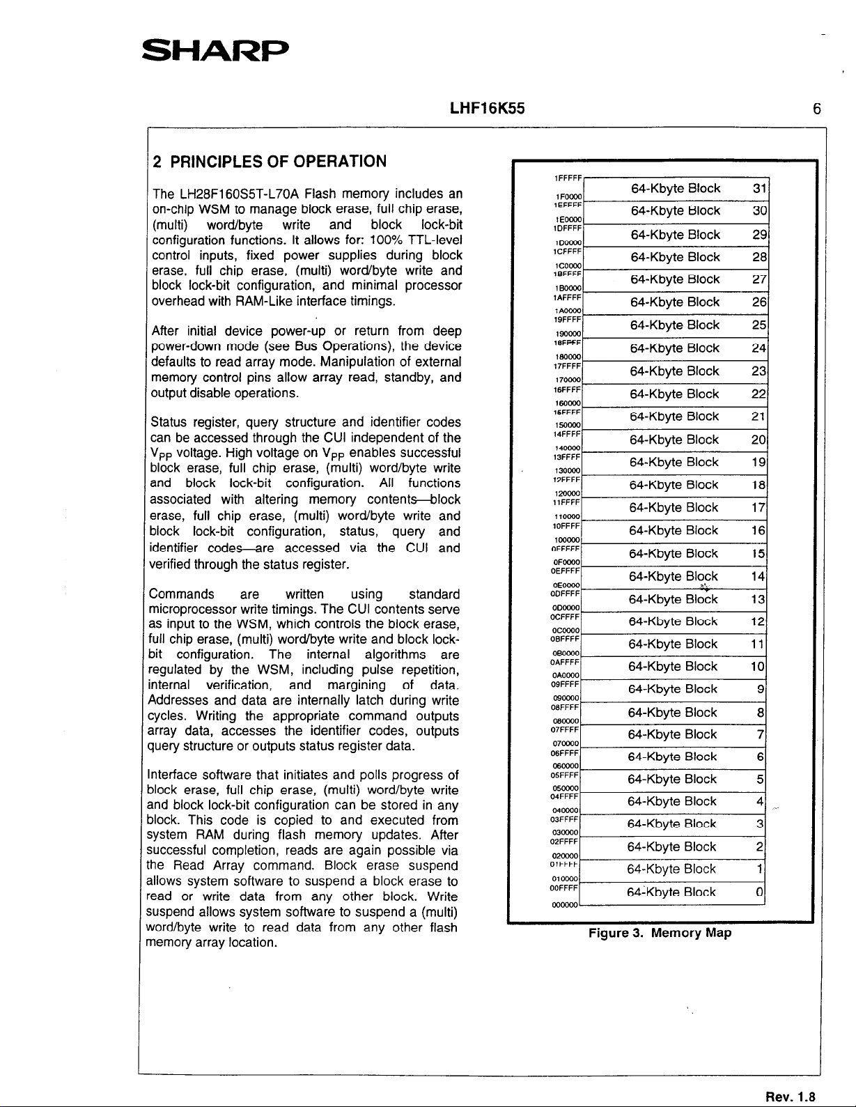
1 .l Product Overview
The LH28F160S5T-L70A is a high-performance 16-
Mbit Smart 5 Flash memory organized as
2MBx8/1MBxl6. The 2MB of data is arranged in
thirty-two 64-Kbyte blocks which are individually
erasable, lockable, and unlockable in-system. The
memory map is shown in Figure 3.
Smart 5 technology provides a choice of Vcc and
V,, combinations, as shown in Table 1, to meet
system performance and power expectations. 5V Voc
provides the highest read performance. V,, at 5V
eliminates the need for a separate 12V converter,
while V,,=5V maximizes erase and write
performance. In addition to flexible erase and
program voltages, the dedicated V,, pin gives
complete data protection when V,, < VppLK.
Table 1. V,, and VP, Voltage Combinations
Offered by Smart 5 Technology
Vcr: Voltage Vpp Voltage
5v 5v
Internal
automatically configures the device for optimized
read and write operations.
A Command User Interface (CUI) serves as the
interface between the system processor and internal
operation of the device. A valid command sequence
nritten to the CUI initiates device automation. An
nternal Write State Machine (WSM) automatically
executes the algorithms and timings necessary for
slack erase, full chip erase, (multi) word/byte write
and block lock-bit configuration operations.
4 block erase operation erases one of the device’s
?4-Kbyte blocks typically within 0.34s (5V Vcc, 5V
Jpp) independent of other blocks. Each block can be
ndependently erased 100,000 times (3.2 million
Ilock erases per device). Block erase suspend mode
1110~s system software to suspend block erase to
,ead or write data from any other block.
4 word/byte write is performed in byte increments
ypically within 9.241s (5V Vco, 5V VP,). A multi
vord/byte write has high speed write performance of
!us/byte (5V Voc, 5V V,,). (Multi) Word/byte write
cuspend mode enables the system to read data or
vcc
and
detection Circuitry
VW
execute code from any other flash memory array
location.
Individual block locking uses a combination of bits
and WP#, Thirty-two block lock-bits, to lock and
unlock blocks. Block lock-bits gate block erase, full
chip erase and (multi) word/byte write operations.
Block lock-bit configuration operations (Set Block
Lock-Bit and Clear Block Lock-Bits commands) se1
and cleared block lock-bits.
The status register indicates when the WSM’s block
erase, full chip erase, (multi) word/byte write or block
lock-bit configuration operation is finished.
The STS output gives an additional indicator of WSM
activity by providing both a hardware signal of status
(versus software polling) and status masking
(interrupt masking for background block erase, for
example). Status polling using STS minimizes both
CPU overhead and system power consumption. STS
pin can be configured to different states using the
Configuration command. The STS pin defaults to
RY/BY# operation. When low, STS indicates that the
WSM is performing a block erase, full chip erase,
(multi) word/byte write or block lock-bit configuration.
STS-High Z indicates that the WSM is ready for a
new command, block erase is suspended and (multi)
word/byte write are inactive, (m!&i) word/byte write
are suspended, or the device is In deep power-down
mode. The other 3 alternate configurations are all
pulse mode for use as a system interrupt.
The access time is 70ns (t,vQv) over the commercial
temperature range (0% to +70X) and Vcc supply
voltage range of 4.75V-5.25V. At lower Vcc voltage,
the access time is 80ns (4.5V-5.5V).
The Automatic Power Savings (APS) feature
substantially reduces active current when the device
is in static mode (addresses not switching). In APS
mode, the typical lCCR current is 1 mA at 5V Vcc.
When either CE,# or CE,#, and RP# pins are at Vco,
the I,, CMOS standby mode is enabled. When the
RP# pin is at GND, deep power-down mode is
enabled which minimizes power consumption and
provides write protection during reset. A reset time
(t,,o,) is required from RP# switching high until
outputs are valid. Likewise, the device has a wake
time (tPHEL) from RP#-high until writes to the CUI are
recognized. With RP# at GND, the WSM is reset and
the status register is cleared.
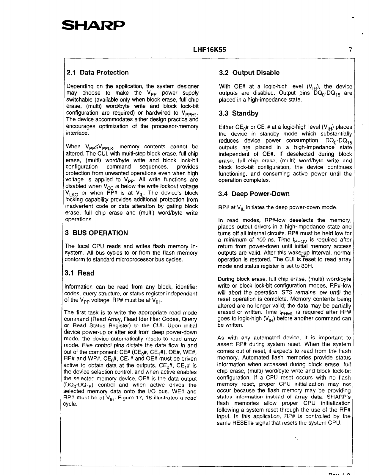
The device is available in 56-Lead TSOP (Thin Small
Outline Package, 1.2 mm thick). Pinout is shown in
Figure 2.
Rev. 1.8
Page 6
SHARP
LHF16K55
r
CE#
WE#
OE%
RPX
WPX
c&
NC
A20
49
Ala
A17
A16
vcc
4s
A14
A13
A12
CE,,#
VPP
RP#
41
ho
AQ
43
GND
A7
A6
A5
%
A3
A2
Al
2
3
4
5
6
7
a
9
10
11
12
13
14
15
16
17
18
19
20
21
22
23
24
25
26
27
28
0
Figure 1. Block Diagram
56 LEAD TSOP
STANDARD PINOUT
14mm x 20mm
TOP VIEW
WP#
WE#
OE#
STS
DQts
DQ7
DQ14
%I
DQ13
DQ5
DQ12
DQ4
vcc
GND
DQll
Ei:,
DQa
vcc
DQ9
DQI
DQs
DQo
A0
BYTE#
NC
NC
Figure 2. TSOP 56-Lead Pinout (Normal Bend)
Rev. 1.8
Page 7
SHARP
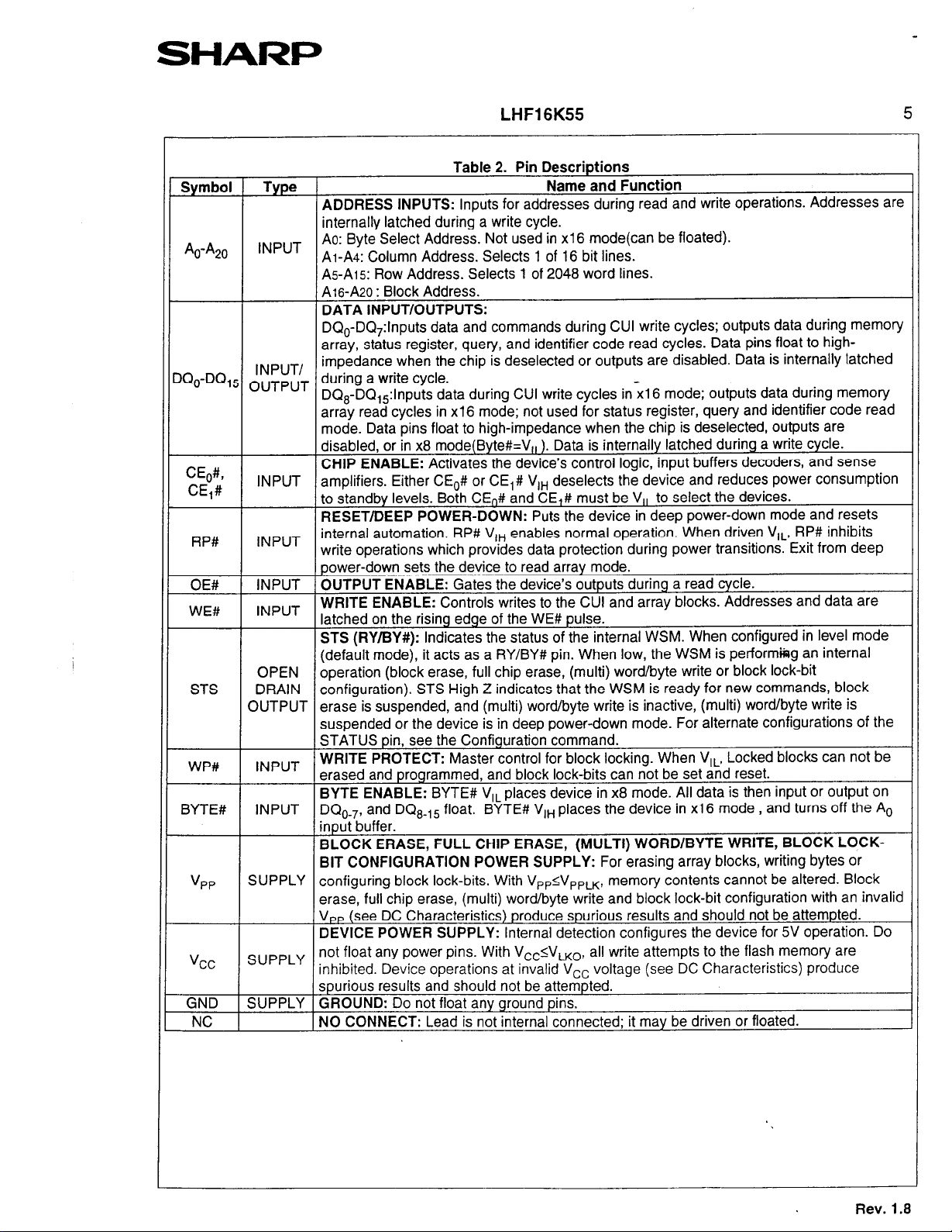
LHF16K55 5
elects 1 of 2048 word lines.
commands during CUI write cycles; outputs data during memory
ower-down mode. For alternate configurations of the
laces the device in xl 6 mode
or eraslng
NC 1 NO CONNECT: Lead is not internal connected; it may be driven or floated.
array
, and turns off the A
Rev.1.8
Page 8
SHARP
2 PRINCIPLES OF OPERATION
The LH28F160!35T-L70A Flash memory includes an
on-chip WSM to manage block erase, full chip erase,
(multi) word/byte
write and block
configuration functions. It allows for: 100% TTL-level
control inputs, fixed power supplies during block
erase, full chip erase, (multi) word/byte write and
block lock-bit configuration, and minimal processor
overhead with RAM-Like interface timings.
After initial device power-up or return from deep
power-down mode (see Bus Operations), the device
defaults to read array mode. Manipulation of external
memory control pins allow array read, standby, and
output disable operations.
Status register, query structure and identifier codes
:an be accessed through the CUI independent of the
VP, voltage. High voltage on VP, enables successful
>lock erase, full chip erase, (multi) word/byte write
lnd block lock-bit configuration. All functions
associated with altering memory contenttilock
erase, full chip erase, (multi) word/byte write and
Ilock lock-bit configuration, status, query and
dentifier codes-are accessed via the CUI and
verified through the status register.
lock-bit
LHF16K55 6
Commands are written using
standard
nicroprocessor write timings. The CUI contents serve
1s input to the WSM, which controls the block erase,
ull chip erase, (multi) word/byte write and block lock-
Iit configuration. The internal algorithms are
egulated by the WSM, including pulse repetition,
nternal verification, and margining of data.
lddresses and data are internally latch during write
:ycles. Writing the appropriate command outputs
array data, accesses the identifier codes, outputs
luery structure or outputs status register data.
nterface software that initiates and polls progress of
block erase, full chip erase, (multi) word/byte write
nd block lock-bit configuration can be stored in any
Ilock. This code is copied to and executed from
ystem RAM during flash memory updates. After
uccessful completion, reads are again possible via
ne Read Array command. Block erase suspend
illows system software to suspend a block erase to
ead or write data from any other block. Write
suspend allows system software to suspend a (multi)
vord/byte write to read data from any other flash
nemory array location.
o7oooo
OGFFFF
06ooOO
05FFFF
o5oooo
04FFFF
o4mo
OBFFFF
030000,
OZFFFF
o2owo _
OlFFFF
o1ocoo.
OOFFFF
WOO00
64-Kbyte Block 7
64-Kbyte Block
64-Kbyte Block
64-Kbyte Block
6CKbyte Block 3
64-Kbyte Block
64-Kbyte Block
64LKbyte Block
Figure 3. Memory Map
6
5
4
2
1
0
Rev. 1.8
Page 9
SHARP
LHF16K55
2.1 Data Protection
Depending on the application, the system designer
may choose to make the Vnp power supply
switchable (available only when block erase, full chip
erase, (multi) word/byte write and block lock-bit
configuration are required) or hardwired to VPPH1.
The device accommodates either design practice and
encourages optimization of the processor-memory
interface.
When Vpp~VppLK,
altered. The CUI, with multi-step block erase, full chip
erase, (multi) word/byte write and block lock-bit
configuration command sequences, provides
orotection from unwanted operations even when high
voltage is applied to V,,. All write functions are
disabled when Vcc is below the write lockout voltage
v,,, or when RP# is at V,,. The device’s block
ocking capability provides additional protection from
nadvertent code or data alteration by gating block
erase, full chip erase and (multi) word/byte write
operations.
memory contents cannot be
3 BUS OPERATION
The local CPU reads and writes flash memory insystem. All bus cycles to or from the flash memory
:onform to standard microprocessor bus cycles.
3.1 Read
nformation can be read from any block, identifier
:odes, query structure, or status register independent
)f the V,, voltage. RP# must be at V,,.
-he first task is to write the appropriate read mode
:ommand (Read Array, Read Identifier Codes, Query
jr Read Status Register) to the CUI. Upon initial
levice power-up or after exit from deep power-down
node, the device automatically resets to read array
node. Five control pins dictate the data flow in and
ut of the component: CE# (CE,#, CE,#), OE#, WE#,
IP# and WP#. CEo#, CE,# and OE# must be driven
ctive to obtain data at the outputs. CE,#, CE,# is
le device selection control, and when active enables
ie selected memory device. OE# is the data output
3Qc-DQ,,) control and when active drives the
elected memory data onto the I/O bus. WE# and
tP# must be at V,,. Figure 17, 18 illustrates a read
ycle.
3.2 Output Disable
With OE# at a logic-high level (VI,), the device
outputs are disabled. Output pins DQc-DQ,, arc
placed in a high-impedance state.
3.3 Standby
Either CE,# or CE,# at a logic-high level (V,,) place:
the device in standby mode which substantial11
reduces device power consumption. DQc-DQ,,
outputs ar_e placed in a high-impedance state
independent of OE#. If deselected during bloc1
erase, full chip erase, (multi) word/byte write ant
block lock-bit configuration, the device continue:
functioning, and consuming active power until the
operation completes.
3.4 Deep Power-Down
RP# at V,, initiates the deep power-down mode.
In read modes, RP#-low deselects the memory
places output drivers in a high-impedance state ant
turns off all internal circuits. RP# must be held low for
a minimum of 100 ns. Time tnHav is required after
return from power-down until initial memory access
outputs are valid. After this wake$p interval, norma
operation is restored. The GUI is reset to read array
mode and status register is set to 80H.
During block erase, full chip erase, (multi) word/byte
write or block lock-bit configuration modes, RP#-low
will abort the operation. STS remains low until the
reset operation is complete. Memory contents being
altered are no longer valid; the data may be partially
erased or written. Time tPHWL is required after RP#
goes to logic-high (V,,) before another command can
be written.
As with any automated device, it is important to
assert RP# during system reset. When the system
comes out of reset, it expects to read from the flash
memory. Automated flash memories provide status
information when accessed during block erase, full
chip erase, (multi) word/byte write and block lock-bit
configuration. If a CPU reset occurs with no flash
memory reset, proper CPU initialization may not
occur because the flash memory may be providing
status information instead of array data. SHARP’s
flash memories allow proper CPU initialization
following a system reset through the use of the RP#
input. In this application, RP# is controlled by the
same RESET# signal that resets the system CPU.
Rev. 1.8
Page 10
SHARI=
LHF16K55
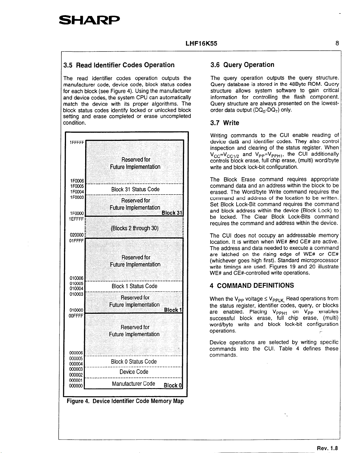
,5 Read Identifier Codes Operation
ie read identifier codes operation outputs the
anufacturer code, device code, block status codes
r each block (see Figure 4). Using the manufacturer
rd device codes, the system CPU can automatically
atch the device with its proper algorithms. The
sck status codes identify locked or unlocked block
!tiing and erase completed or erase uncompleted
ndition.
8
3.6 Query Operation
The query operation outputs the query structure.
Query database is stored in the 48Byte ROM. Query
structure allows system software to gain critica,
information for controlling the flash component.
Query structure are always presented on the lowestorder data output (DC&,-DQ,) only.
3.7 Write
Writing commands to the CUI enable reading oi
device data and identifier codes. They also control
inspection and clearing of the status register. When
Vcc=Vcc,,2 and VPP=VPPH1, the CUI additionally
controls block erase, full chip erase, (multi) word/byte
write and block lock-bit configuration.
The Block Erase command requires appropriate
command data and an address within the block to be
erased. The Word/byte Write command requires the
command and address of the location to be written.
Set Block Lock-Bit command requires the command
and block address within the device (Block Lock) to
be locked. The Clear Block Lock-Bits command
requires the command and address within the device.
‘igure 4. Device Identifier Code Memory Map
The CUI does not occupy an addressable memory
location. It is written when WE# &rd CE# are active.
The address and data needed to execute a command
are latched on the rising edge of WE# or CE#
(whichever goes high first). Standard microprocessor
write timings are used. Figures 19 and 20 illustrate
WE# and CE#-controlled write operations.
4 COMMAND DEFINITIONS
When the V,, voltage 2 V,,,,, Read operations from
the status register, identifier codes, query, or blocks
are enabled. Placing VppHl on V,, :enables
successful block erase, full chip erase, (multi)
word/byte write and block lock-bit configuration
operations.
Device operations are selected by writing specific
commands into the CUI. Table 4 defines these
commands.
.r
Rev. 1.8
Page 11
SHARf=
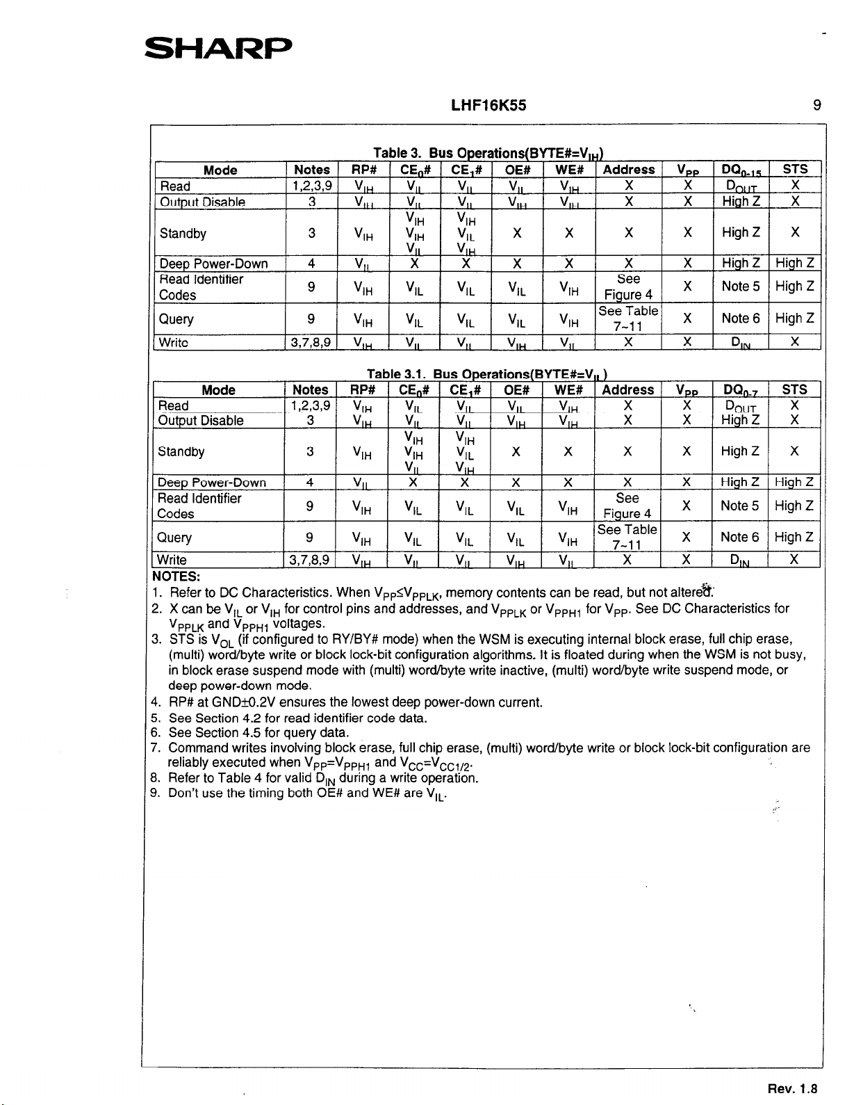
Mode
Read
Output Disable
LHF16K55
Table 3. Bus Operations(BYTE#=V,,)
Notes 1 RP# 1 CE,,# 1 CE,# OE# 1 WE# I Address
1
12733
3
3
4
9
!L
IIH-
“I,
v,,
“I,
v,,
v,,
“I,
“1,
ll!ll-
“IL
X
v,,
v,,
“I,
“IL
l!lH-
X X
“IL
V,, V,H
V,&j V,w
X
“IL
X
X
“I,
1 Vpp 1 DQn.,5 I STS ]
1 X Dn,,r
X
X High Z X
X
High Z X
X High Z High Z
X Note 5 High Z
X
9
3,mg
RB
NOTES:
1. Refer to DC Characteristics. When V,,<V,,,k,
2. X can be V,, or VrH for control pins and addresses, and V,,,, or VPPHt for V,,. See DC Characteristics for
V,nLk and V,r+n voltages.
3. STS is V,, (if configured to RY/BY# mode) when the WSM is executing internal block erase, full chip erase,
(multi) word/byte write or block lock-bit configuration algorithms. It is floated during when the WSM is not busy,
in block erase suspend mode with (multi) word/byte write inactive, (multi) word/byte write suspend mode, or
deep power-down mode.
4. RP# at GNDM.2” ensures the lowest deep power-down current.
5. See Section 4.2 for read identifier code data.
6. See Section 4.5 for query data.
7. Command writes involving block erase, full chip erase, (multi) word/byte write or block lock-bit configuration are
reliably executed when VPP=VPPH1 and Vcc=Vcc,,2.
8. Refer to Table 4 for valid D,, during a write operation.
9. Don’t use the timing both OE# and WE# are VI,.
“I,
L!k.
“IL
I
“IL
V
E
memory contents can be read, but not altere%f:
“I,
v,r
X Note 6 High Z
X D,N X
.,--
Rev. 1.8
Page 12
SHARP
LHF16K55
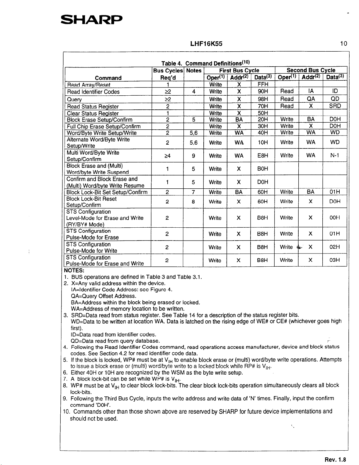
Table 4. Commanc .
Bus Cycles Notes
Command
Read Array/Reset
Read Identifier Codes
Al lternate Word/Byte Write
Setup/Write Multi Word/Byte Write
Setup/Confirm
Block Erase and (Multi)
Word/byte Write Suspend
Confirm and Block Erase and
(Multi) Word/byte Write Resume
Block Lock-Bit Set Setup/Confirm
Block Lock-Bit Reset
Setup/Confirm
STS Confiauration
Level-Mode for Erase and Write 1 2 1 I Write I X
(RY/BY# Mode)
STS Confiauration
Pulse-Mode for Erase
STS Configuration
Pulse-Mode for Write
STS Configuration
Pulse-Mode for Erase and Write
IOTES:
. BUS operations are defined in Table 3 and Table 3.1.
. X=Any valid address within the device.
IA=ldentifier Code Address: see Figure 4.
QA=Query Offset Address.
BA=Address within the block being erased or locked.
WA=Address of memory location to be written.
3
. SRD=Data read from status register. See Table 14 for a description of the status register bits.
WD=Data to be written at location WA. Data is latched on the rising edge of WE# or CE# (whichever goes high
first).
ID=Data read from identifier codes.
QD=Data read from query database.
. Following the Read Identifier Codes command, read operations access manufacturer, device and block status
codes. See Section 4.2 for read identifier code data.
. If the block is locked, WP# must be at VI, to enable block erase or (multi) word/byte write operations. Attempts
to issue a block erase or (multi) word/byte write to a locked block while RP# is V,,.
. Either 40H or 1OH are recognized by the WSM as the byte write setup.
A block lock-bit can be set while WP# is V,,.
. WP# must be at V,, to clear block lock-bits. The clear block lock-bits operation simultaneously clears all block
lock-bits.
9.
Following the Third Bus Cycle, inputs the write address and write data of ‘N’ times. Finally, input the confirm
command ‘DOH’.
II
3. Commands other than those shown above are reserved by SHARP for future device implementations and
should not be used.
Req’d
1 WI,., , ,\ , I.II ,
I
2
14
1 5 Write X BOH
2 8 Write
z vvnte A aan
2
2 Write X B8H
4 I Write I X 1 90H 1 Read 1
5,6
9
7 Write
1 Definitions(lO)
First Bus Cycle
VU) ( Ad&(*) 1 Data@) Ope#) ) AI
opt
ritn
1 Y 1 FFU I
Write
Write
Write
Write X
WA
WA
BA 2
10H
E8H
DOH 1 5 Write
I B8H I Write I X I OOH /
B8H Write b : X 02H
Second
Write WA WD
Write
Write
vvrw A Ull-l
Write X 03H
I Bus Cycle
ddr(*) Datat3)
4
4 ID
WA N-l
BA
X
7.-
Rev. 1.8
Page 13
SHARP
LHF16K55 11
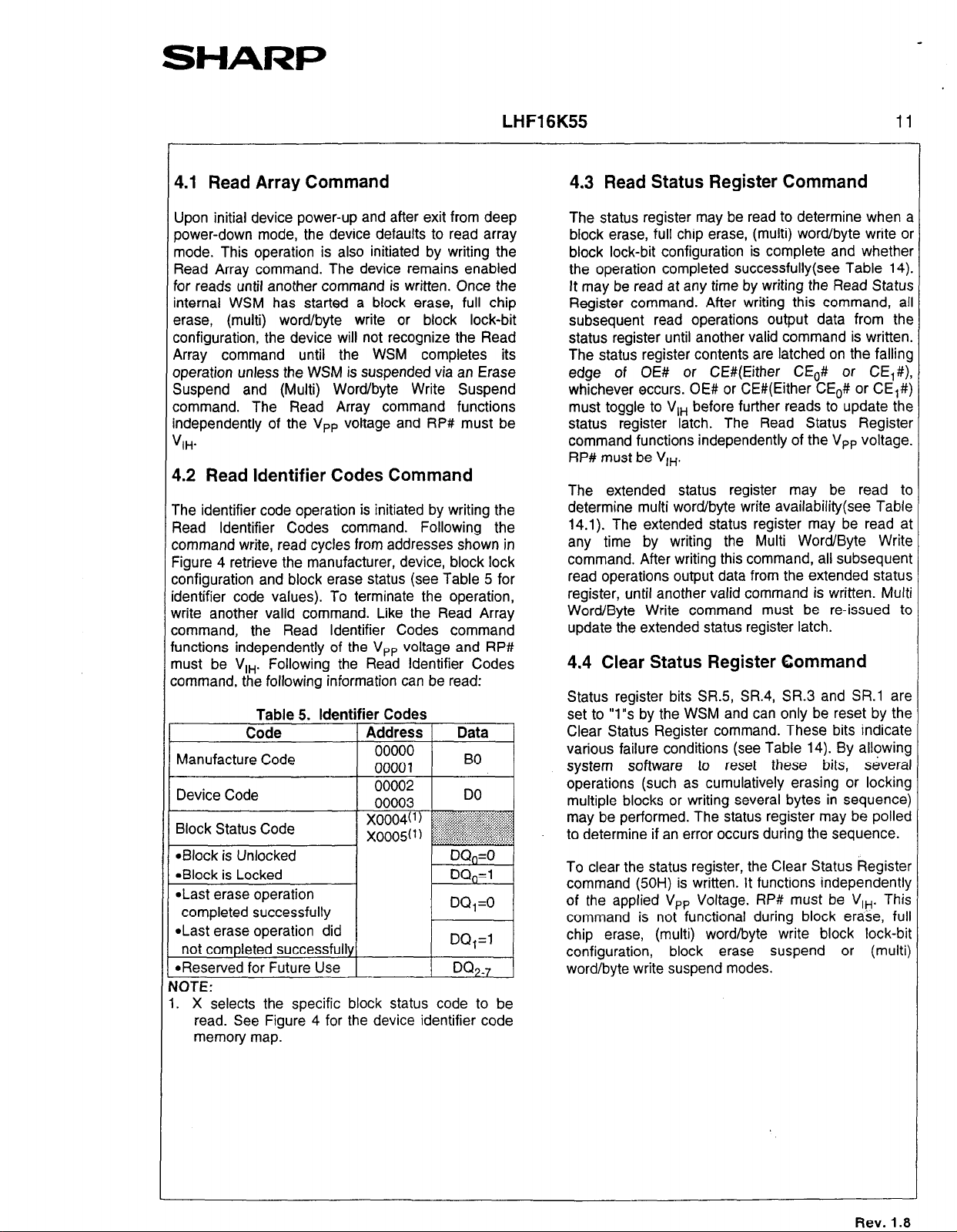
4.1 Read Array Command 4.3 Read Status Register Command
Upon initial device power-up and after exit from deep
power-down mode, the device defaults to read array
mode. This operation is also initiated by writing the
Read Array command. The device remains enabled
for reads until another command is written. Once the
internal WSM has started a block erase, full chip
erase, (multi) word/byte write or block lock-bit
configuration, the device will not recognize the Read
Array command until the WSM completes its
operation unless the WSM is suspended via an Erase
Suspend and (Multi) Word/byte Write Suspend
command. The Read Array command functions
ndependently of the Vpp
VIH-
voltage and RP# must be
1.2 Read Identifier Codes Command
The identifier code operation is initiated by writing the
qead Identifier Codes command. Following the
:ommand write, read cycles from addresses shown in
7gure 4 retrieve the manufacturer, device, block lock
:onfiguration and block erase status (see Table 5 for
dentifier code values). To terminate the operation,
Nrite another valid command. Like the Read Array
:ommand, the Read Identifier Codes command
unctions independently of the V,, voltage and RP#
nust be Vi,. Following the Read Identifier Codes
:ommand, the following information can be read:
Table 5. Identifier Codes
Code
Manufacture Code
Device Code
Block Status Code
1 Address 1 Data 1
I nr\nnn
““““”
nnnn 1
The status register may be read to determine when i
block erase, full chip erase, (multi) word/byte write OI
block lock-bit configuration is complete and whethel
the operation completed successfully(see Table 14)
It may be read at any time by writing the Read Statu$
Register command. After writing this command, al
subsequent read operations output data from the
status register until another valid command is written
The status register contents are latched on the fallin<
edge of OE# or CE#(Either CEc# or CE,#)
whichever eccurs. OE# or CE#(Either CE,# or CE,#:
must toggle to VrH before further reads to update the
status register latch. The Read Status Register
command functions independently of the V,, voltage
RP# must be V,,.
The extended status register may be read tc
determine multi word/byte write availability(see Table
14.1). The extended status register may be read ai
any time by writing the Multi Word/Byte Writs
command. After writing this command, all subsequeni
read operations output data from the extended status
register, until another valid command is written. Mutt1
Word/Byte Write command must be re-issued tc
update the extended status register latch.
4.4 Clear Status Register Command
Status register bits SR.5, SR.4, SR.3 and SR.l are
set to “1”s by the WSM and can only be reset by the
Clear Status Register command. These bits indicate
various failure conditions (see Table 14). By allowing
system software to reset these bits, several
operations (such as cumulatively erasing or locking
multiple blocks or writing several bytes in sequence)
may be performed. The status register may be polled
to determine if an error occurs during the sequence.
*Last erase operation did
not completed successfully
*Reserved for Future Use
IOTE:
X selects the specific block status code to be
read. See Figure 4 for the device identifier code
memory map.
DC!,=1
DQ?-,
To clear the status register, the Clear Status Register
command (50H) is written. It functions independently
of the applied V,, Voltage. RP# must be V,,. This
command is not functional during block erase, full
chip erase, (multi) word/byte write block lock-bii
configuration, block erase suspend or (multi)
word/byte write suspend modes.
Rev. 1.8
Page 14
SHARP
LHF16K55 12
1.5 Query Command
Juery database can be read by writing Query
:ommand (98H). Following the command write, read
ycle from address shown in Table 7-11 retrieve the
xitical information to write, erase and otherwise
:ontrol the flash component. A, of query offset
tddress is ignored when X8 mode (BYTE#=V,L).
Juery data are always presented on the low-byte
fata output (D&JDQ,). In x16 mode, high-byte
DQs-DQ,,) outputs OOH. The bytes not assigned to
iny information or reserved for future use are set to
0”. This command functions independently of the
Ipp voltage. RP# must be V,,.
Table 6. Example of Query Structure Output
Mode Off set Address
A,, A,, A,, A2, A, t A,
1 , 0 , 0 , 0 , 0 , 0 (20H) High-Z
X8mode 1 ,O,O,O,O,l (21H) High-Z
1, O,O,O,l ,0(22H) High-Z
1 , 0 , 0 , 0 , 1 , 1 (23H) High-Z “R”
Xl6 mode 1 , 0 , 0 , 0 , 0 (10H) OOH “0”
A,, A,, A,, A,,
l,O,O,O,l (11H) OOH “R”
A,
output
DQ, q-~ DQ7-c
“Q”
“Q”
“R”
1.5.1 Block Status Register
-his field provides lock configuration and erase status for the specified block. These informations are only availabk
vhen device is ready (SR.7=1). If block erase or full chip erase operation is finished irregulary, block erase statu.
bit will be set to “1”. If bit 1 is “l”, this block is invalid.
Table 7. Query Block Status Register
Off set
(Word Address)
(BA+2)H OlH Block Status Register
lote:
. BA=The beginning of a Block Address.
Length
bit0 Block Lock Configuration
O=Block is unlocked
l=Block is Locked
bit1 Block Erase Status
O=Last erase operation completed successfully
l=Last erase operation not completed successfully
bit2-7 reserved for future use
Description
%g.
Rev. 1.8
Page 15
SHARP
LHF16K55
13
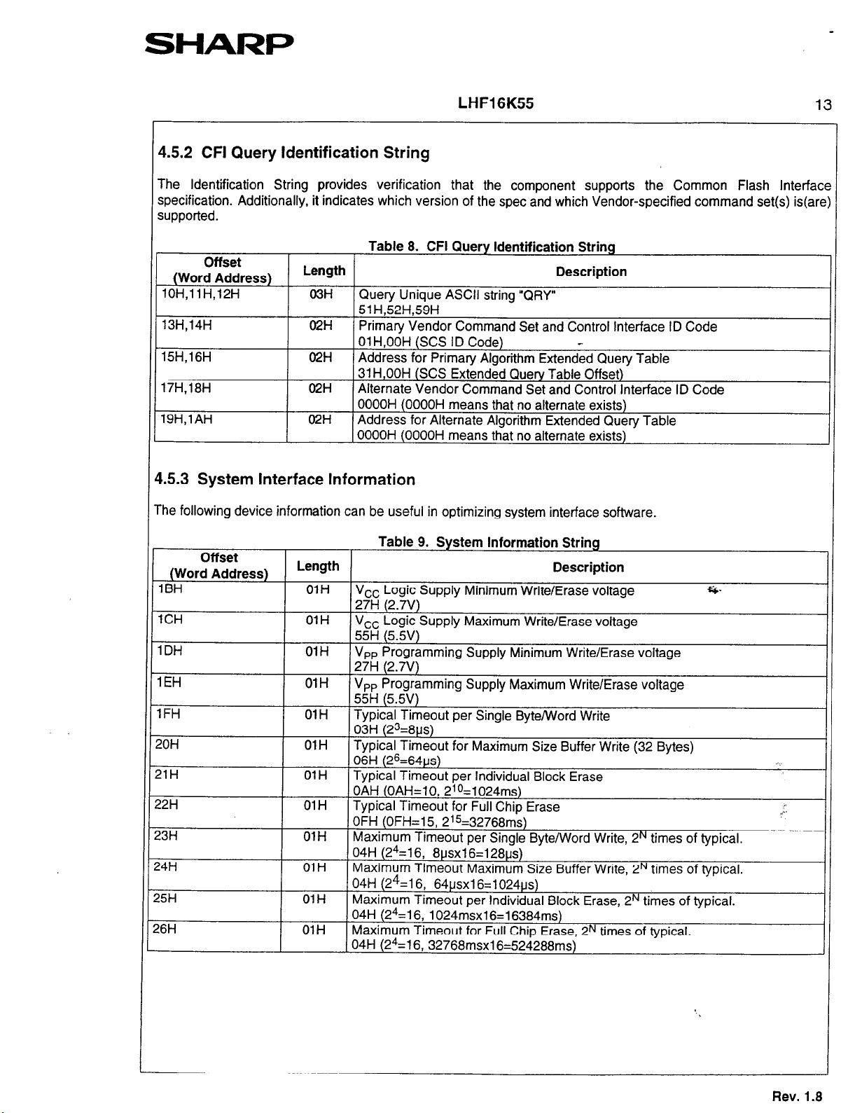
4.52 CFI Query Identification String
The Identification String provides verification that the component supports the Common Flash Interface
specification. Additionally, it indicates which version of the spec and which Vendor-specified command set(s) is(are)
supported.
Table 8. CFI Query Identification String
Offset
(Word Address)
lOH,l lH,l2H
13H,l4H
15H,l6H
17H,l8H
lSH,lAH
Length
WH Query Unique ASCII strinq “QRY”
51 H,52H,59H
02H Primary Vendor Command Set and Control Interface ID Code
01 H,OOH (SCS ID Code)
02H Address for Primary Algorithm Extended Query Table
31 H,OOH (SCS Extended Query Table Offset)
02H Alternate Vendor Command Set and Control Interface ID Code
OOOOH (OOOOH means that no alternate exists)
02H Address for Alternate Algorithm Extended Query Table
OOOOH (OOOOH means that no alternate exists)
Description
4.5.3 System Interface Information
The following device information can be useful in optimizing system interface software.
Offset
(Word Address)
1BH
1CH
1DH
1EH
1FH
20H
21H
22H
23H
24H
25H
26H
Table 9. System Information String
Length Description
01H Vcc Logic Supply Minimum Write/Erase voltage
27H (2.7V)
OlH Vcc Logic Supply Maximum Write/Erase voltage
55H (5.5V)
OlH V,, Programming Supply Minimum Write/Erase voltage
27H (2.7V)
OlH V,, Programming Supply Maximum Write/Erase voltage
55H (5.5V)
OlH Typical Timeout per Single Byte/Word Write
03H (23=8us)
01H Typical Timeout for Maximum Size Buffer Write (32 Bytes)
06H (26=64us)
OlH Typical Timeout per Individual Block Erase
OAH (OAH=lO, 210=1024ms)
OlH
01H Maximum Timeout per Single Byte/Word Write, 2N times of typical.
OlH Maximum Timeout Maximum Size Buffer Write, 2N times of typical.
01H
01H Maximum Timeout for Full Chip Erase, 2N times of typical.
Typical Timeout for Full Chip Erase
OFH (OFH=15, 215=32768ms)
04H (24=1 6, 8usxl6=128us)
04H (24=1 6, 64usxl6=1024us)
Maximum Timeout per Individual Block Erase, 2N times of typical.
04H (24=1 6, 1024msx16=16384ms)
04H (24=1 6,32768msxl6=524288ms)
+i;.
,i-
Rev. 1.8
Page 16
SHARP
LHF16K55
14
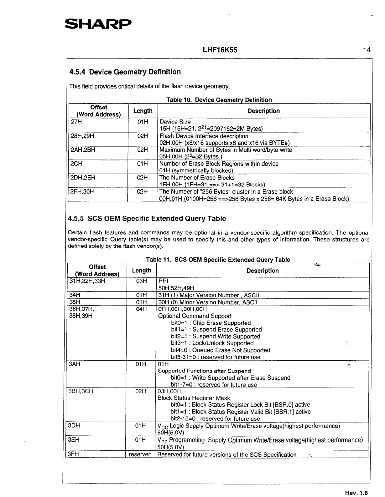
4.5.4 Device Geometry Definition
This field provides critical details of the flash device geometry.
Table 10. Device Geometry Definition
Offset
(Word Address)
27H 01H Device Size
28H,29H 02H Flash Device Interface description
2AH,2BH 02H Maximum Number of Bytes in Multi word/byte write
2CH
2DH,2EH 1 02H 1 The Number of Erase Blocks
2FH,30H
Length
15H (15H=21, 22i=2097152=2M Bytes)
02H,OOH (x8/x1 6 supports x8 and xl 6 via BYTE#)
05H,OOH (2s=32 Bytes )
OlH Number of Erase Block Regions within device
1 01 H (symmetrically blocked)
1 FH,OOH (1 FH=31 ==> 31 +1=32 Blocks)
02H The Number of “256 Bytes” cluster in a Erase block
OOH,Ol H (01 OOH=256 ==>256 Bytes x 256~ 64K Bytes in a Erase Block)
Description
1.5.5 SCS OEM Specific Extended Query Table
Zertain flash features and commands may be optional in a vendor-specific algorithm specification. The optional
rendor-specific Query table(s) may be used to specify this and other types of information. These structures are
defined solely by the flash vendor(s).
Offset
(Word Address)
31 H,32H,33H
34H
35H
36H,37H,
38H,39H
3AH
3BH,3CH
3DH
IEH
3FH
Table 11. SCS OEM Specific Extended Query Table
Length
03H PRI
50H,52H,49H
OlH
OlH 30H (0) Minor Version Number, ASCII
04H OFH,OOH,OOH,OOH
OlH OlH
02H 03H,OOH
OlH Vco Logic Supply Optimum Write/Erase voltage(highest performance)
OlH V,, Programming Supply Optimum Write/Erase voltage(highest performance)
reserved Reserved for future versions of the SCS Specification
31H (1) Major Version Number, ASCII
Optional Command Support
bitO=l : Chip Erase Supported
bit1 =l : Suspend Erase Supported
bit2=1 : Suspend Write Supported
bit3=1 : LocWUnlock Supported
bit4=0 : Queued Erase Not Supported
bit531 =O : reserved for future use
Supported Functions after Suspend
bitO=l : Write Suooorted after Erase Susoend
bit1 -7=O : reserved for future use
Block Status Register Mask
bitO=l : Block Status Register Lock Bit [BSR.O] active
bitl=l : Block Status Register Valid Bit [BSR.l] active
bit2-15=0 : reserved for future use
50H(5.OV)
50H(5.OV)
Description
’
‘I
*.
!i-
Rev. 1.8
Page 17

SHARP
LHF16K55
4.6 Block Erase Command
Block erase is executed one block at a time and
initiated by a two-cycle command. A block erase
setup is first written, followed by an block erase
confirm. This command
appropriate sequencing and an address within the
block to be erased (erase changes all block data to
FFH). Block preconditioning, erase and verify are
handled internally by the WSM (invisible to the
system). After the two-cycle block erase sequence is
written, the device automatically outputs status
register data when read (see Figure 5). The CPU can
detect block erase completion by analyzing the
output data of the STS pin or status register bit SR.7.
When the block erase is complete, status register bit
SR.5 should be checked. If a block erase error is
detected, the status register should be cleared before
system software attempts corrective actions. The CUI
?emains in read status register mode until a new
:ommand is issued.
This two-step command sequence of set-up followed
)y execution ensures that block contents are not
lccidentally erased. An invalid Block Erase command
sequence will result in both status register bits SR.4
lnd SR.5 being set to “1 I’. Also, reliable block erasure
:an only occur when Vcc=Vcc1,2 and VPP=VPPH1. In
he absence of this high voltage, block contents are
lrotected against erasure. If block erase is attempted
vhile V,+V,,,,, SR.3 and SR.5 will be set to “1”.
successful
:orresponding block lock-bit be cleared or if set, that
rVP#=V,,. If block erase is attempted when the
:orresponding block lock-bit is set and WP#=V,,,
jR.1 and SR.5 will be set to “I”.
block erase requires that the
sequence requires
I.7 Full Chip Erase Command
erase setup is first written, followed by a full chi
erase confirm. After a confirm command is writter
device erases the all unlocked blocks from block 0 t
Block 31 block by block. This command sequenc#
requires appropriate
preconditioning, erase and verify are handle1
internally by the WSM (invisible to the system). Afte
the two-cycle full chip erase sequence is written, thl
device automatically outputs status register dat;
when read (see Figure 6). The CPU can detect fu
chip erase completion by analyzing the output data c
the STS pin or status register bit SR.7.
When the full chip erase is complete, status registe
bit SR.5 should be checked. If erase error i:
detected, the status register should be cleared befort
system software attempts corrective actions. The CU
remains in read status register mode until a nev
command is issued. If error is detected on a bloc1
during full chip erase operation, WSM stops erasing
Reading the block valid status by issuing Read II:
Codes command or Query command informs which
blocks failed to its erase.
This two-step command sequence of set-up follower
by execution ensures that block contents are no
accidentally erased. An invalid Full Chip Erase
command sequence will result in both status registe
bits SR.4 and SR.5 being set to “&‘!. Also, reliable ful
chip erasure can only occur when Vcc=Vcc1,2 ant
VPP=VPPHi-
contents are protected against erasure. If full chir
erase is attempted while Vpp~Vpp,,, SR.3 and SR.!
will be set to “1”. When WP#=V,,, all blocks arc
erased independent of block lock-bits status. Wher
WP#=V,,, only unlocked blocks are erased. In thi:
case, SR.l and SR.4 will not be set to “1“. Full chir
erase can not be suspended.
In the absence of this high voltage, bloc1
sequencing.
Bloc
‘his command followed by a confirm command
30H) erases all of the unlocked blocks. A full chip
Rev. 1.8
Page 18

SHARP
LHF16K55
4.8 Word/Byte Write Command
Word/byte write is executed by a two-cycle command
sequence. Word/Byte Write setup (standard 40H or
alternate 10H) is written, followed by a second write
that specifies the address and data (latched on the
rising edge of WE#). The WSM then takes over,
controlling the word/byte write and write verify
algorithms internally. After the word/byte write
sequence is written, the device automatically outputs
status register data when read (see Figure 7). The
CPU can detect the completion of the word/byte write
event by analyzing the STS pin or status register bit
SR.7.
When word/byte write is complete, status register bit
SR.4 should be checked. If word/byte write error is
detected, the status register should be cleared. The
Internal WSM verify only detects errors for “1”s that
do not successfully write to “0%. The CUI remains in
,ead status register mode until it receives another
zommand.
qeliable word/byte writes can only occur when
Jcc=Vcc1,2 and VPP=VPPH1. In the absence of this
iigh voltage, memory contents are protected against
Nerd/byte writes. If word/byte write is attempted while
J,,IV,,,,, status register bits SR.3 and SR.4 will be
set to “1”.
he corresponding block lock-bit be cleared or, if set,
hat WP#=V,,. If word/byte write is attempted when
he corresponding block lock-bit is set and WP#=V,,,
jR.1 and SR.4 will be set to “1”. Word/byte write
operations with V,,<WP#<V,, produce spurious
esults and should not be attempted.
Successful word/byte write requires that
16
continue monitoring XSR.7 by writing multi word/byte
write setup with write address until XSR.7 transitions
to 1. When XSR.7 transitions to 1, the device is reac
for loading the data to the buffer. A word/byte COUI
(N)-1 is written with write address. After writing
word/byte count(N)-1, the device automatically turn
back to output status register data. The word/byl
count (N)-1 must be less than or equal to IFH in x
mode (OFH in x16 mode). On the next write, devic
start address is written with buffer data. Subsequer
writes provide additional device address and datz
depending on the count. All subsequent addres
must lie within the start address plus the count. Aftc
the final buffer data is written, write confirm (Dot-
must be written. This initiates WSM to begin copyin
the buffer data to the Flash Array. An invalid Mul
Word/Byte Write command sequence will result i
both status register bits SR.4 and SR.5 being set t
“1”. For additional multi word/byte write, write anoths
multi word/byte write setup and check XSR.7. Th
Multi Word/Byte Write command can be queue
while WSM is busy as long as XSR.7 indicates “1’
because LH28F160S5T-L70A has two buffers. If a
error occurs while writing, the device will stop writin
and flush next multi word/byte write command loadeN
in multi word/byte write command. Status register b
SR.4 will be set to “1”. No multi word/byte writ1
command is available if either SR.4 or SR.5 are SE
to “1”. SR.4 and SR.5 should %e cleared befort
issuing multi word/byte write command. If a mul
word/byte write command is attempted past an eras
block boundary, the device will write the data to Flasl
Array up to an erase block boundary and then stol
writing. Status register bits SR.4 and SR.5 will be SE
to “1 I’.
IY
It
a
IS
:e
8
e
1t
1,
S
1;
9
ti
n
0
?r
:
8,
I;
:
it
e
?t
e
ti
;
P
!t
I.9 Multi Word/Byte Write Command
Aulti word/byte write is executed by at least four:ycle or up to 35cycle command sequence. Up to
12 bytes in x8 mode (16 words in xl 6 mode) can be
laded into the buffer and written to the Flash Array.
Yrst, multi word/byte write setup (E8H) is written with
ie write address. At this point, the device
utomatically outputs extended status register data
KSR) when read (see Figure 8, 9). If extended
‘atus register bit XSR.7 is 0, no Multi Word/Byte
/rite command is available and multi word/byte write
?tup which just has been written is ignored. To retry,
Reliable multi byte writes can only occur wher
Vcc=Vc-.,,2 and VPP=VPPH1. In the absence of thi:
high voltage, memory contents are protected agains
multi word/byte writes. If multi word/byte write i:
attempted while V,,<V,,,,, status register bits SR.:
and SR.4 will be set to “1”. Successful mull
word/byte write requires that the corresponding bloc1
lock-bit be cleared or, if set, that WP#=V,,. If mull
byte write is attempted when the corresponding bloc1
lock-bit is set and WP#=V,,, SR.l and SR.4 will bc
set to “1 ‘I.
Rev. 1.8
n
S
it
S
3
ti
k
ti
I,
Page 19

SHARP
LHF16K55
4.10 Block Erase Suspend Command
The Block Erase Suspend command allows block-
erase interruption to read or (multi) word/byte-write
data in another block of memory. Once the blockerase process starts,
Suspend command requests that the WSM suspend
the block erase sequence at a predetermined point in
the algorithm. The device outputs status register data
when read after the Block Erase Suspend command
is written. Polling status register bits SR.7 and 33.6
can determine when the block erase operation has
been suspended (both will be set to “1”). STS will
also transition to High-Z. Specification twHRH2
defines the block erase suspend latency.
At this point, a Read Array command can be written
to read data from blocks other than that which is
suspended. A (Multi) WordByte Write command
sequence can also be issued during erase suspend
to program data in other blocks. Using the (Multi)
Word/Byte Write Suspend command (see Section
4.1 l), a (multi) word/byte write operation can also be
suspended. During a (multi) word/byte write operation
with block erase suspended, status register bit SR.7
will return to “0” and the STS (if set to RY/BY#)
output will transition to V,. However, SR.6 will
remain “1” to indicate block erase suspend status.
The only other valid commands while block erase is
suspended are Read Status Register and Block
Erase Resume. After a Block Erase Resume
command is written to the fiash memory, the WSM
will continue the block erase process. Status register
Sits SR.6 and SR.7 will automatically clear and STS
will return to VOL. After the Erase Resume command
IS written, the device automatically outputs status
register data when read (see Figure IO). V,, must
remain at V,,,, (the same V,, level used for block
arase) while block erase is suspended. RP# must
also remain at V,,. Block erase cannot resume until
writing the Block Erase
17
(multi) word/byte write operations initiated during
block erase suspend have completed.
4.11 (Multi) Word/Byte Write Suspend
Command
The (Multi) Word/Byte Write Suspend command
allows (multi) word/byte write interruption to read data
in other flash memory locations. Once the (multi)
word/byte write process starts, writing the (Multi)
Word/Byte Write Suspend command requests that
the WSM suspend the (multi) word/byte write
sequence ‘at a predetermined point in the algorithm.
The device continues to output status register data
when read after the (Multi) Word/Byte Write Suspend
command is written. Polling status register bits SR.7
and SR.2 can determine when the (multi) word/byte
write operation has been suspended (both will be set
to “1”). STS will also transition to High-Z.
Specification twHRH, defines the (multi) word/byte
write suspend latency.
At this point, a Read Array command can be written
to read data from locations other than that which is
suspended. The only other valid commands while
(multi) word/byte write is suspended are Read Status
Register and (Multi) Word/Byte Write Resume. After
(Multi) Word/Byte Write Resumecommand is written
to the flash memory, the WSM’will continue the
(multi) word/byte write process. Status register bits
SR.2 and SR.7 will automatically clear and STS will
return to VOL. After the (Multi) Word/Byte Write
command is written, the device automatically outputs
status register data when read (see Figure 11). V,,
must remain at V,,,, (the same V,, level used for
(multi) word/byte write) while in (multi) word/byte
write suspend mode. WP# must also remain at V,, or
VI,.
Rev. 1.8
Page 20

SHARP
LHF16K55
4.12 Set Block Lock-Bit Command
A flexible block locking and unlocking scheme is
enabled via block lock-bits. The block lock-bits gate
program and erase operations With WP#=V,,,
individual block lock-bits can be set using the Set
Block Lock-Bit command. See Table 13 for a
summary of hardware and software write protection
options.
Set block lock-bit is executed by a two-cycle
command sequence. The set block lock-bit setup
along with appropriate block or device address is
Nritten followed by either the set block lock-bit
:onfirm (and an address within the block to be
ocked). The WSM then controls the set block lock-bit
algorithm. After the sequence is written, the device
automatically outputs status register data when read
:see Figure 12). The CPU can detect the completion
If the set block lock-bit event by analyzing the STS
)in output or status register bit SR.7.
Nhen the set block lock-bit operation is complete,
status register bit SR.4 should be checked. If an error
s detected, the status register should be cleared.
The CUI will remain in read status register mode until
1 new command is issued.
‘his two-step sequence of set-up followed by
execution ensures that block lock-bits are not
tccidentalfy set. An invalid Set Block Lock-Bit
:ommand will result in status register bits SR.4 and
sR.5 being set to “1”. Also, reliable operations occur
only when Vcc=Vcc,,2 and VPP=VPPH1. In the
absence of this high voltage, block lock-bit contents
Ire protected against alteration.
18
block lock-bits can be cleared using only the Clea
Block Lock-Bits command. See Table 13 for ;
summary of hardware and sofhvare write protectiol
options.
Clear block lock-bits operation is executed by a two
cycle command sequence. A clear block lock-bit!
setup is first written. After the command is written, the
device automatically outputs status register dat:
when read (see Figure 13). The CPU can detec
completion of the clear block lock-bits event bl
analyzing the STS Pin output or status register bi
SR.7. -
When the operation is complete, status register bi
SR.5 should be checked. If a clear block lock-bit erro
is detected, the status register should be cleared
The CUI will remain in read status register mode unti
another command is issued.
This two-step sequence of set-up followed b\
execution ensures that block lock-bits are no
accidentally cleared. An invalid Clear Block Lock-Bit:
command sequence will result in status register bit:
SR.4 and SR.5 being set to “1”. Also, a reliable cleai
block lock-bits operation can only occur wher
Vcc=Vcc1,2 and VPP=VPPH1. If a clear block lock-bit2
operation is attempted while VpplVppLK, SR.3 ant
SR.5 will be set to “1”. In the a&ence of this higt
voltage, the block lock-bits content are protectec
against alteration. A successful clear block lock-bit:
operation requires WP#=V,,. If it is attempted witt-
WP#=V,,, SR.l and SR.5 will be set to “1” and the
operation will fail. Clear block lock-bits operations
with V,,cRP# produce spurious results and shoulc
not be attempted.
I successful set block lock-bit operation requires
VP#=V,,. If it is attempted with WP#=V,,, SRI and
iR.4 will be set to “1” and the operation will fail. Set
‘lock lock-bit operations with WP#cV,, produce
purious results and should not be attempted.
#.I3 Clear Block Lock-Bits Command
/II set block lock-bits are cleared in parallel via the
:lear Block Lock-Bits command. With WP#=V,,,
If a clear block lock-bits operation is aborted due tc
V,, or V,, transitioning out of valid range or RP#
active transition, block lock-bit values are left in an
undetermined state. A repeat of clear block lock-bits
is required to initialize block lock-bit contents tc
known values.
Rev. 1.8
Page 21

SHARP
LHF16K55
4.14 STS Configuration Command
The Status (STS) pin can be configured to different
states using the STS Configuration command. Once
the STS pin has been configured, it remains in that
configuration until another configuration command is
issued, the device is powered down or RP# is set to
V,,. Upon initial device power-up and after exit from
deep power-down mode, the STS pin defaults to
RY/BY# operation where STS low indicates that the
WSM is busy. STS High Z indicates that the WSM is
ready for a new operation.
To reconfigure the STS pin to other modes, the STS
Sonfiguration is issued followed by the appropriate
zonfiguration code. The three alternate configurations
are all pulse mode for use as a system interrupt. The
STS Configuration command functions independently
3f the V,, voltage and RP# must be VI,.
Table 12. STS Configuration Coding Description
Configuration
Bits
OOH
OlH
02H
03H
L
Set STS pin to default level mode
(RY/BY#). RY/BY# in the default
level-mode of operation will indicate
WSM status condition.
Set STS pin to pulsed output signal
for specific erase operation. In this
mode, STS provides low pulse at
the completion of BLock Erase,
Full Chip Erase and Clear Block
Lock-bits operations.
Set STS pin to pulsed output signal
for a specific write operation. In this
mode, STS provides low pulse at
the completion of (Multi) Byte Write
and Set Block Lock-bit operation.
Set STS pin to pulsed output signal
for specific write and erase
operation. STS provides low pulse
at the completion of Block Erase,
Full Chip Erase, (Multi) Word/Byte
Write and Block Lock-bit
Configuration operations.
Effects
19
Operation
Block Erase, 0
(Multi) Word/Byte
Write
Full Chip Erase
Set Block Lock-Bit X
Clear Block Lock-Bits
Block
Lock-Bit
071
X V,w All blocks are erased
X
Table 13. Write Protection Alternatives
WP# Effect
V,, or VI,, Block Erase and (Multi) Word/Byte Write Enabled
1
VI,
VI,
V,, All unlocked blocks are erased, locked blocks are not erased
V,, Set Block Lock-Bit Disabled
V,# , Set Block Lock-Bit Enabled
V,,
V,, Clear Block Lock-Bits Enabled
Block is Locked. Block Erase and (Multi) Word/Byte Write
Disabled
Block Lock-Bit Override. Block Erase and (Multi) Word/Byte
Write Enabled
Clear Block Lock-Bits Disabled
4.
.,--
Rev. 1.8
Page 22

SHARI=
1
LHF16K55
Table 14. Status Register Definition
WSMS )
7
SR.7 = WRITE STATE MACHINE STATUS
1 = Ready
0 = Busy
SR.6 = BLOCK ERASE SUSPEND STATUS
1 = Block Erase Suspended
0 = Block Erase in Progress/Completed
SR.5
= ERASE AND CLEAR BLOCK LOCK-BITS
STATUS
1 = Error in Erase or Clear Bloc1 Lock-Bits
0 = Successful Erase or Clear Block Lock-Bits
SR.4 = WRITE AND SET BLOCK LOCK-BIT STATUS
1 = Error in Write or Set Block Lock-Bit
0 = Successful Write or Set Block Lock-Bit
SR.3
= V,p STATUS
1 = V,, Low Detect, Operation Abort
O=V,,OK
SR.2 = WRITE SUSPEND STATUS
1 = Write Suspended
0 = Write in Progress/Completed
SR.l = DEVICE PROTECT STATUS
1 = Block Lock-Bit and/or WP# Lock Detected,
Operation Abort
0 = Unlock
SR.0 = RESERVED FOR FUTURE ENHANCEMENTS
BESS
6 5
( ECBLBS 1 WSBLBS [ VPPS 1 wss
4
20
DPS R
3
NOTES:
Check STS or SR.7 to determine block erase, full chip
erase, (multi) word/byte write or block lock-bit
configuration completion.
SR.6-0 are invalid while SR.7=“0”.
If both SR.5 and SR.4 are “1% after a block erase, full
chip erase, (multi) word/byte write, block lock-bit
configuration or STS configuration attempt, an improper
command sequence was entered.
SR.3 does not provide a continuous indication of V,,
level. The WSM interrogates and indicates the V,, level
only after block erase, full chip erase, (multi) word/byte
write or block lock-bit configuration command
sequences. SR.3 is not guaranteed to reports accurate
feedback only when V,,+V,,,,.
SRI does not provide a continuous indication of block
lock-bit values. The WSM interrogates block lock-bit,
and WP# only after block erase, full chip erase, (multi)
word/byte write or block lock-bit configuration command
sequences. It informs the system, depending on the
attempted operation, if the block lock-bit is set and/or
WP# is not V,,. Reading the block lock configuration
codes after writing the Read Identifier Codes command
indicates block lock-bit status.
SR.0 is reserved for future use and should be masked
out when polling the status register.
2
1
0
1
Table 14.1. Extended Status Register Definition
SMS
7 6
GR.7 = STATE MACHINE STATUS
1 = Multi Word/Byte Write available
0 = Multi Word/Byte Write not available
(SRG-O=RESERVED FOR FUTURE ENHANCEMENT,
R
R R R
5 4
R
3
NOTES:
After issue a Multi Word/Byte Write command: XSR.7
indicates that a next Multi Word/Byte Write command is
available.
XSR.G-0 is reserved for future use and should be
masked out when polling the extended status register.
2 1
R R
0
.-.
Rev. 1.8
II
Page 23

SHARP
LHF16K55
]
Block Address
Check if Desired
FULLSTANSCHECKPROCEDURE
Read
Erase Setup
Wnte
Read / 1 Status Register Data
Repeat for subsequent block etasures.
Full otatus check can be done after each block emse or after a sequence of
block erasures.
Write FFH after the
Ease
confirm
last
operation to place device in read army mode.
Status Regrster Data
Data+UH
Add,=Within Block to be Erased
Data..DOH
Ad-z&Within Block to be Erased
Standby
Standby
ck-diie Protect Error
Standby
Standby
SR.S.SR.4.SR.J and SR. 1 are only cleared by the Clear Status
Register Command in cases where multiple blocks are erased
Sbck Erase Error
before full status is checked.
f arror is detected. clear the Status Register before attempting
retry or other error recovery.
Figure 5. Automated Block Erase Flowchart
Comments
Check SR.3
lnVpp Error Detect
Check SR. 1
l=Device Protect Detect
WP#=V,,.Block Lock-Sit is Set *’
Only required for systems
implementing lock-bit confgurabon
Check SR.4.5
Both l=Command Sequence Error
Check SR.5
l=Blcck Erase Error
.+.
r
Rev. 1.8
Page 24

SHARP
starI
f
Write 70H
+
Read stalw
Wile DOH
f
Read status
LHF16K55
Full status dreck can be done alter each full chip arase.
Write FFH after the last operation to place device in read away mode.
Full Status
Check if Desired
+
Block Erase
Ccmplete
FULL STATUS CHECK PROCEDURE
Read Status Regtster
Data(See Above) Command Comments
Check SR.3
trVpp Error Detect
Check SR.4,5
Both l=CommandSquence Error
Check SR.5
l=Bbck Erase Error
Block Erase Error
Standby
Standby
SR.S.SR.4.SR.3 and SR.l are only dewed by the Clear Status
Register Command in cases where multiple blocks are erased
before full stahlr IS checked.
If error is detected. clear the Status Regrster before attempting
retry or olher error r*co”ery.
.Eg,
Block Erase Successful
Figure 6. Automated Full Chip Erase Flowchart
Rev. 1.8
Page 25

SHARI=
Stall
c-
el
LHF16K55
23
1
--I
Read Status
Flsglster Add,=X
Write WordByte write
Read
standby
I I
bpeat for subsequent wordlbyte writes.
jR fulf status check can be done after each w&byte write, or after P sequence of
word4lyta wlites.
Write FFH after me last word~%y?e write operation to place device in
read army mode.
Data-70H
DataData to Be Written
Addr=Localton to Be Written
Status Register Data
Check SR.7
,=WSM Ready
O=WShl Busy
FULL STATUS CHECK PROCEDURE
Read Status Register
Data(See Above)
standty
m
Device Pmtect Error
Standby
jR.4.SR.3 and SR.1 are only cleared by the Clear Stahn Register
command in cases where multiple locations are written before
full status is checked.
I error is detected. clear the St&s Register before attempting
retry or other *rrOr recovery.
Figure 7. Automated Word/byte Write Flowchart
Command
Check SR.3
t=Vpp Error Detect
implementing lock-bit configuration
/
Check SR.4
t=Data Write Error
n--
Rev. 1.8
Page 26

SHARP
‘I
Write EBH.
Start Address
+
Reed stetus
Rsglster
Wnte Buffer Data,
Start Address
A
wnta Another
Block Address.
LHF16K55
Bus
opaelion
Write
Reed
stemby
Write
wote2.3)
Read Status Register Data
Command
SUP
~ufti WordlByte Write Ad&Start Address
Data=EBH
Extended Status Register Data
Check XSR.7
tMul6 WordByte Wdte Ready
O=Mulb woldmyte write Busy
Data=Word or Byte Count (N)-1
Add,-Start Address
Dala=Suffer Data
Add&tart Address
DatazBuffer Data
Add,=Dsvne Address
Data=DOH
Addr=X
Comments
24
Write Buffer Data.
Dew% Address
Check if Dewed
Standby
1. Syta or word count values on DClo., are loaded into the count register.
2. Write Suffer contents will be programmed at the start address.
3. Align the start address on a Write Buffer boundary for maximum
pmgramming parfonance.
4.The device aborts the Multi Word/Byte Write command if the current address is
outs!& of the original block address.
5% Status Register indicates an ‘improper command sequence’ if the Multi
WorrVeyte command is aborted. Follow this mm a Clear Stahls Register command.
SR full statis check can be done after each multi worclbyte write.
or after a sequence of multi worcubyte writes.
Write FFH after the Iat muili word/byte write cfzeratnon to place device m
reed may mode.
Check SR.7
1.WSM Ready
c=WSM BUSY &$*
Figure 8. Automated Multi Word/Byte Write Flowchart
Rev. 1.8
Page 27

SHARI=
FULL STATUS CHECK PROCEWRE FOR
MLfLTt WORD/BYTE WRITE OPERATlON
Road status Reglrter
Dwce Protect Enor
LHF16K55 25
Elm
Opmrtion
Stan&y
standby
Command
Check SR.3
,=Vpp Error Detect
Check SR.1
I=Dome Pmtect Detect
WPX-VIL.Blcck Lock-Bit IS Set
Only required for oyttems
implementing lock-bit configuration
Check SR.4.5
Boti l-Command Sequence Error
Commcnb
standby
SR.S.SR.4.SFt.3 and SR.1 are only deamd by the Clear S&IS Register
command in cases where multiple locations are wlitten before
lull status is checked.
If ~rmr ia detected, clear the Stahts Register before attemptmg
retry or other elmr recwefy.
Check SR.4
tdlata Write Error
Figure 9. Full Status Check Procedure for Automated Multi Word/Byte Write
L
Rev. 1.8
Page 28

SHARP
LHF16K55
Check SR.7
l=WSM Ready
O=WSM Busy
Read Array Data
4 (Multi) WcdByte write LOOP I
Figure 10. Block Erase Suspend/Resume Flowchart
smldby
Write
Check SIT.6
l=Slock Erase Suspended
O-Block Erase Completed
EtXe DaQDOH
Resume
Add-X
Rev. 1.8
Page 29

SHARP
LHF16K55 27
Comments
Wnta BOH
(Ml&l) wofveyte write
Completed
Data&OH
Addr=X
Status Register Data
Add-X
Check SR.7
Standby
I-
standby
Write Read Amy
l--L
Read
Write
E
(Multi) word/Byte wmt
Resume
l=WSM Ready
O-WSM Busy
Chedc SR.2
b(Mulb) Word/Byte Write
suspwldsd
OS(MUlti) wotdmyte write
Compkdd
Data=FFH
Addr-X
Road Array locations other
than tiat being written.
Datad30k-l
AddbX
Figure 11. (Multi) Word/Byte Write Suspend/Resume Flowchart
Rev. 1.8
Page 30

SHARP
LHF16K55
Write OlH.
Block Address
I
g +
NLL STATUS CHECK PROCEDURE
I
Read
Status Register
SR.7= SR.7=
1 1
Check If Desired
Read Status Register
Data&See Above)
0 0
Bus
OprMfOll
write
Read
Standby
Repeat for subsequent Mock lock-bit set operations.
%II status chedc can b-a done after each block lock-bit set operation
or after a sequence of block lock-bit set operations.
Write FFH after the last block bck-bit set operation to place device in
read amay mode.
BUS
opsrrtfon
I
Standby
commnd Comments
Set Bock
Lock-Bit Confirm
Command Commentr
I
Data-01 H.
Add&lock Address
Stabs Register Data
Check SR.7
l=WSM Ready
o=WSM Busy
Check SR.3
tsVpp Error Detect
*-
Set Black Lock-EN
successful
Device Protect Error
Figure 12. Set Block Lock-Bit Flowchart
Standby
SR.S.SR.4.SR.3 and SR.1 are onfy deared by the Clear Status
Register command in cases where multiple block lock-bits are set before
full status is checked.
If error is detected, dear the St&s Register before attempting
retry or omer em, recovaly.
Check SR.4
l=Set Block Lock-Sit Error
Rev. 1.8
Page 31

SHARI=
LHF16K55
Write 60H
Write DOH
Full Status
Check 11 Dewed
Clear Block Lock-Bit
Complete
FULL STATUS CHECK PROCEDURE
Read Status Regiriter
Data(See Above)
Bus
OpNrtiOll
Write
Write
Read
Standby
Write FFH after the Clear Block Lock-Bib operahon to
place device in read array mode.
BUS
OpadiOll
Standby
Command
Clear Block
Lock-Bits Setup
Clear Blcck
Lock-Bits Confin
Command
Data&OH
Addr=X
Da&ZWH
Add,=X
St&s Register Data
Check SR.7
1PwsM Ready
O-WSM Busy
Check SR.3
lz.Vpp Error Detect
Commmb
Comments
a$<
Device Protect Enor
Figure 13. Clear Block Lock-Bits Flowchart
Check SR.l
smdby
Standby
standby
SR.S.SR.4.SR.3 and SR.l are only cleared by the Clear Status
Regster command.
If ermr is detected. clear the Status Register before attempbng
retry 0, omer mm, recovely.
t-Device Pmtect Detect
WP#‘V,L
Check SR.4.5
Both t=Command
Sequence Ermr
Check SR.5
t&tear Block Lock-Bits Error
Rev. 1.8
Page 32

SHARP
LHFl6K55
5 DESIGN CONSIDERATIONS
5.1 Three-Line Output Control
The device will often be used in large memory arrays.
SHARP provides three control inputs to
accommodate multiple memory connections. ThreeLine control provides for:
a. Lowest possible memory power dissipation.
b. Complete assurance that data bus contention will
not occur.
To use these control inputs efficiently, an address
decoder should enable CE# while OE# should be
connected to all memory devices and the system’s
READ# control line. This assures that only selected
memory devices have active outputs while
deselected memory devices are in standby mode.
RP# should be connected to the system
DOWERGOOD signal to prevent unintended writes
during system power transitions. POWERGOOD
should also toggle during system reset.
5.2 STS and Block Erase, Full Chip
Erase, (Multi) Word/Byte Write and
Block Lock-Bit Configuration Polling
STS is an open drain output that should be
:onnected to Vcc y b a pullup resistor to provide a
iardware method of detecting block erase, full chip
erase, (multi) word/byte write and block lock-bit
:onfiguration completion. In default mode, it
ransitions low after block erase, full chip erase,
multi) word/byte write or block lock-bit configuration
:ommands and returns to VOH when the WSM has
inished executing the internal algorithm. For
Ilternate
;onfiguration command.
STS pin
configurations,
see the
STS, in default mode, is also High-Z when the device
is in block erase suspend (with (multi) word/byte write
inactive), (multi) word/byte write suspend or deer
power-down modes.
5.3 Power Supply Decoupling
Flash memory power switching characteristics require
careful device decoupling. System designers are
interested in three supply current issues; standby
current levels, active current levels and transienl
peaks produced by falling and rising edges of CE#
and OE#. Transient current magnitudes depend on
the device outputs’ capacitive and inductive loading.
Two-line control and proper decoupling capacitor
selection will suppress transient voltage peaks. Each
device should have a 0.1 uF ceramic capacitor
connected between its Vcc and GND and between its
V,, and GND. These high-frequency, low inductance
capacitors should be placed as close as possible to
package leads. Additionally, for every eight devices,
a 4.7 uF electrolytic capacitor should be placed at the
array’s power supply connection between Vcc and
GND. The bulk capacitor will overcome voltage
slumps caused by PC board trace inductance.
5.4 Vpp Trace on Printed Circuit Boards
Updating flash memories that r&side in the target
system requires that the printed circuit board
designer pay attention to the V,, Power supply trace.
The V,, pin supplies the memory cell current for
block erase, full chip erase, (multi) word/byte write
and block lock-bit configuration. Use similar trace
widths and layout considerations given to the Vcc
power bus. Adequate V,, supply traces and
decoupling will decrease V,, voltage spikes and
overshoots.
;TS can be connected to an interrupt input of the
system CPU or controller. It is active at all times.
Rev. 1.8
Page 33

LHF16K55
31
5.5 VCC, Vpp, RP# Transitions
Block erase, full chip erase, (multi) word/byte write
and block lock-bit configuration are not guaranteed if
V,, falls outside of a valid V,,,, range, Vc, falls
outside of a valid V,,,,z range, or RP#=V,,. If V,,
error is detected, status register bit SR.3 is set to “1”
along with SR.4 or SR.5, depending on the attempted
operation. If RP# transitions to VI, during block
erase, full chip erase, (multi) word/byte write or block
lock-bit configuration, STS(if set to RY/BY# mode)
will remain low until the reset operation is complete.
Then, the operation will abort and the device will
enter deep power-down. The aborted operation may
leave data partially altered. Therefore, the command
sequence must be repeated after normal operation is
restored. Device power-off or RP# transitions to VI‘
clear the status register.
The CUI latches commands issued by system
software and is not altered by V,, or CE# transitions
or WSM actions. Its state is read array mode upon
lower-up, after exit from deep power-down or after
dcc transitions below V,ko.
After block erase, full chip erase, (multi) word/byte
write or block lock-bit configuration, even after V,,
ransitions down to V,,,,,
‘ead array mode via the Read Array command if
subsequent access to the memory array is desired.
the CUI must be placed in
5.6 Power-Up/Down Protection
-he device is designed to offer protection against
rccidental block and full chip erasure, (multi)
vord/byte writing or block lock-bit configuration during
rower transitions. Upon power-up, the device is
ldifferent as to which power supply (V,, or Voo)
powers-up first. Internal circuitry resets the CUI to
read array mode at power-up.
A system designer must guard against spuriou
writes for Vcc voltages above VLKO when V,, i
active. Since both WE# and CE# must be low for ;
command write, driving either to V,, will inhibit writes
The CUl’s two-step command sequence architecture
provides added level of protection against dat;
alteration.
In-system block lock and unlock capability prevent
inadvertent data alteration. The device is disablec
while RP#=V,, regardless of its control inputs state.
5.7 Power Dissipation
When designing portable systems, designers mus
consider battery power consumption not only durin!
device operation, but also for data retention durin:
system idle time. Flash memory’s nonvolatiliQ
increases usable battery life because data is retainer
when system power is removed.
In addition, deep power-down mode ensure:
extremely low power consumption even when systen
power is applied. For example, portable computing
products and other power sensitive applications tha
use an array of devices for soli&state storage car
consume negligible power by lowering RP# to V,,
standby or sleep modes. If access is again needed
the devices can be read following the t,,av ant
tPHwL wake-up cycles required after RP# is firs
raised to V,,. See AC Characteristics- Read Only
and Write Operations and Figures 17, 18, 19, 20 fol
more information.
Rev. 1.8
Page 34

SHARP
LHFl6K55 32
6 ELECTRICAL SPECIFICATIONS
6.1 Absolute Maximum Ratings*
Commercial Operating Temperature
During Read, Erase, Write and
Block Lock-Bit Configuration . . . . . . ..O”C to +7O”C(‘)
Temperature under Bias . . . . . . . . . . . . . . . -10°C to +8O”C
Storage Temperature . . . . . . . . . . . . . . . . . . . . . . . . -65°C to +125”C
Voltage On Any Pin
(except V,,, V,,) . . . . . . . . . . . . . . . -OS/ to V,,+0.5V(2)
Vcc Suply Voltage . . . . . . . . . . . . . . . . . . . . . . . . . . . . - 0.2v to +7.ov(2)
VP,, Update Voltage during
Erase, Write and
Block Lock-Bit Configuration . . . . ..-0.2V to +7.0Vt2)
3utput Short Circuit Current . . . . . . . . . . . . . . . . . . . . . . . . 100mA(3)
5.2 Operating Conditions
Temperature and V,, 03erating Conditions
Symbol Parameter
Ta Operating Temperature 0
Van, Vcn Supply Voltage (5VkO.25V)
Vnn::, Voc Supply Voltage (5V+O.5V)
Min. Max. Unit Test.Condition
4.75 5.25 V
4.50
‘WARNING: Stressing the device beyond the
“Absolute Maximum Ratings” may cause permanen
damage. These are stress ratings only. Operation
beyond the “Operating Conditions” is no
recommended and extended exposure beyond the
“Operating Conditions” may affect device reliability.
NOTES:
1. Operating temperature is for commercial produc
defined by this specification.
2. All specified voltages are with respect’to GND
Minimum DC voltage is -0.5V on input/output pim
and -0.2V on V,-c and V,, pins. During
transitions, this level may undershoot to -2.OV foi
periods <20ns. Maximum DC voltage or
input/output pins and Vc, is V,c+O.5V which
during transitions, may overshoot to Vcc+2.OL
for periods <20ns.
3. Output shorted for no more than one second. NC
more than one output shorted at a time.
+70 “C
5.50 V
Ambient Temperature
5.2.1 CAPACITANCE(‘)
Symbol Parameter
C,N Input Capacitance
Cn, ,T Output Capacitance
IOTE:
. Sampled, not 100% tested.
T,=+25”C, f=l MHz
Typ. Max.
7
9 12
10
Unit Condition
pF v,N=o.ov
pF Vnr ,T=O.OV
Rev. 1.8
Page 35

SHARP
LHF16K55
82.2 AC INPUT/OUTPUT TEST CONDITIONS
~~~Ty~~~)(z-
AC test inputs are driven at 3.OV for a Logic “1” and O.OV for a Logic “0.” Input timing begins, and output timing ends, at 1.W.
Input rise and fall times (10% to 90%) 40 ns.
Figure 14. Transient Input/Output Reference Waveform for V,.+V*O.25V
(High Speed Testing Configuration)
o;;T-x-yyz~)(-yc
AC test inputs are driven at VOH (2.4 Vm) for a Logic “1” and VOL (0.45 V~L) for a Logic “0.” Input timing begins at VIH
(2.0 Vm) and VIL (0.8 Vrn). Output timing ends at VIH and VIL. Input rise and fall times (10% to 90%) ~10 ns.
Figure 15. Transient Input/Output Reference Waveform for Vc+k0.5V
(Standard Testing Configuration)
33
1.3v
-T
IN914
f
yJgo OUT
L
Capacitance
Figure 16. Transient Equivalent Testing
-IL
-
Load Circuit
Test Confi uration Ca acitance Loadin Value
x
Rev. 1.8
Page 36

SHARP
6.2.3 DC CHARACTERISTICS
LHF16K55
DC Characteristics
Rev. 1.8
Page 37

SHARP
LHF16K55
DC Characteristics (Continued)
V,@J Test
Symbol
V,,
VI,
VOL
“OH1
Input Low Voltage 7 -0.5
Input High Voltage
Output Low Voltage
Output High Voltage
mu
VOH2
Output High Voltage
(CMOS) V,,
‘PPLK
VP, Lockout during Normal
Ooerations
vPPHl
VP, during Write or Erase
Operations
v, KO
Vcc Lockout Voltage
IOTES:
. All currents are in RMS unless otherwise noted. Typical values at nominal Vcc voltage and TA=+25”C.These
currents are valid for all product versions (packages and speeds).
* ‘CCWS and ‘CCES
the device’s current draw is the sum of Iccws or lCCEs and lCCR or I,,,, respectively.
. includes STS.
. Block erases, full chip erases, (multi) word/byte writes and block lock-bit configurations are inhibited when
Vpp~VppL,, and not guaranteed in the range between Vp&max) and VppHt (min) and above,VppH, (max).
. Automatic Power Savings (APS) reduces typical lCCR to 1 mA at 5V Vcc in static operation. 9i;.
. CMOS inputs are either Vcc*0.2V or GNDrt0.2V. TTL inputs are either V,, or VI,.
. Sampled, not 100% tested.
Parameter
Notes Min. Max. Unit Conditions
V
V
1 Vcc=VocMin
’ lo, =5.8mA
” p%c~;
OH
” IJcc>5&M;
OH .
Vcc=VccMin
v
IOH=- OOuA
V
7
3,7
3,7
397
4,7
2.0
2.4
0.85
vcc
-0.4
0.8
vcc
+0.5
0.45
1.5
4.5 5.5 V
2.0 V
are specified with the device de-selected. If read or byte written while in erase suspend mode,
35
Rev. 1.8
Page 38

SHARP
LHFI 6K55
6.2.4 AC CHARACTERISTICS - READ-ONLY OPERATIONS(‘)
~ NOTES:
1. See AC Input/Output Reference Waveform for maximum allowable input slew rate.
2. OE# may be delayed up to tELav-t6Lav
3. Sampled, not 100% tested.
4. See Ordering Information for device speeds (valid operational combinations).
5. See Transient Input/Output Reference Waveform and Transient Equivalent Testing Load Cir$u.it (High Speed
Configuration) for testing characteristics.
6. See Transient input/Output Reference Waveform and Transient Equivalent Testing Load Circuit (Standard
Configuration) for testing characteristics.
after the falling edge of CE# without impact on tELQv.
Rev. 1.8
Page 39

SHARP
hi
CEt(E)
ML
VIH
OH(G)
ML
hi
WE#(W)
ML
VOH
DATA(D/Q)
VOL
Standby
Device
Address Selection
Address Stable
r
LHF16K55
1
Data Valid
lalid Output
37
,..I......
kc
tPHQV
VIH
RP#(P)
VIL
NOTE: CE# is defined as the latter of CEo# and CE,# going Low or the first of CEo# or CE# going High.
t
“““““7
Figure 17. AC Waveform for Read Operations
Rev. 1.8
Page 40

SHARP
LHFl6K55
Device
Address Selection
Address Stable
kVAV-,
CWE)
hi
VIL
VIH
4
1
tAVFL=kLFL
l
OE#(G)
VIL
VOH
DATA(D/Q)
PQdQd
VOL
5 . . . . ..I...
NOTE: CE# is defined as the latter of CEo# and CE# going Low or the first of CEo# or CE# going High.
Figure 18. BYTE# Timing Waveforms
HIGH Z
&,.
,’
Rev. 1.8
Page 41

SHARP
LHF16K55
r
3.2.5 AC CHARACTERISTICS -WRITE OPERATIONS(‘)
V,+V*O.SV, SV~O.25V, TpO”C to +70X
Vcc*0.25V 1 LH28F16OS5-L70@) [
Version&
Sym. Parameter Notes Min. Max. Min. Max. Unit
tAVAjJ Write Cycle Time
tPHWL
RP# High Recovery to WE# Going
Low
v,,*o.5v 1 1 LH28Fi 60S5-L80(7)
70
2 1
80 ns
1
IJS
IOTES:
. Read timing characteristics during block erase, full chip erase, (multi) wrod/byte write and block lock-bit
configuration operations are the same as during read-only operations. Refer to AC Characteristics for read-only
operations.
. Sampled, not 100% tested.
. Refer to Table 4 for valid A,, and D,, for block erase, full chip erase, (multi) word/byte write or block lock-bit
configuration.
. VP, should be held at VppH, until determination of block erase, full chip erase, (multi) word/byte write or block
lock-bit configuration success (SR.1/3/4/5=0).
. See Ordering Information for device speeds (valid operational combinations).
. See Transient Input/Output Reference Waveform and Transient Equivalent Testing Load Circuit (High Seed
Configuration) for testing characteristics.
. See Transient Input/Output Reference Waveform and Transient Equivalent Testing Load Circuit (Standard
Configuration) for testing characteristics.
q,*
Rev. 1.8
Page 42

SHARP
ADDRESSES(A)
CE#U(El
OE#(G)
WEW)
DATA(D/Q)
STS(R)
WP#(S)
LHFl6K55
1 2 3 4 5 6
A-----
hi
VIL
VII-I
ML
VIH
ML
High
“,::r
40
RP#(P)
NOTES:
1. VCC power-up and standby.
2. Write erase or write
3. Write erase confirm or valid address and data.
4. Automated erase or program delay.
5. Read status register data.
6. Write Read Array command.
7. CE# is defined as the latter of CEO# and CEI# going Low or the first of CE& or CE# going High.
setup.
hi
VIL
Figure 19. AC Waveform for WE#-Controlled Write Operations
1.
;.
r
a-
,
Rev. 1.8
Page 43

SHARP
LHF16K55
6.2.6 ALTERNATIVE CE#-CONTROLLED WRITES(‘)
41
NOTES:
1. In systems where CE# defines the write pulse width (within a longer WE# timing waveform), all setup, hold and
inactive WE# times should be mea:ured relative to the CE# waveform.
2. Sampled, not 100% tested.
3. Refer to Table 4 for valid A,, and D,, for block erase, full chip erase, (multi) word/byte write sblock lock-bit
configuration.
4. VP, should be held at VPP,,
lock-bit configuration success (SR.1/3/4/5=0).
5. See Ordering Information for device speeds (valid operational combinations).
6. See Transient Input/Output Reference Waveform and Transient Equivalent Testing Load Circuit (High Seed
Configuration) for testing characteristics.
7. See Transient Input/Output Reference Waveform and Transient Equivalent Testing Load Circuit (Standard
Configuration) for testing characteristics.
until determination of block erase, full chip erase, (multi) word/byte write or block
Rev. 1.8
Page 44

SHARP
ADDRESSES(A)
WWW
OE#(G)
CE#(E)
VIH
VIL
VIH
ML
hi
WL
hi
VIL
LHFl6K55
42
NOTES:
1. Vcc power-up and standby.
2. Write erase or write setup.
3. Write erase confirm or valid address and data.
4. Automated erase or program delay.
5. Read status register data.
6. Write Read Array command.
7. CE# is defined as the latter of CEo# and CE,# going Low or the first of CEo# or CE,# going High.
Figure 20. AC Waveform for CE#-Controlled Write Operations
. . .
C’
Rev. 1.8
Page 45

SHARP
2.7 RESET OPERATIONS
LHF16K55
STS(R)
RP#(P)
STS( R)
RP#(P)
vcc
RP#(P)
High Z
VOL
VIH
WL
High Z
VOL
VIH
WL
5v
VIL
VIH
ML
(A)Reset During Read Array Mode
bLRH
(B)Reset During Block Erase, Full Chip Erase, (Multi) Word/Byte Write
or Block Lock-Bit Configuretion
- kVPH
I
1‘
(C)Vcc Power Up Timing
Figure 21. AC Waveform for Reset Operation
Reset AC Specification&)
V,,=SV
rmbol
-PH
.RH
U-4
Parameter
Notes
RP# Pulse Low Time
(If RP# is tied to Vno, this specification is not applicable)
RP# Low to Reset during Block Erase, Full Chip Erase,
(Multi) Word/Byte Write or Block Lock-Bit Configuration
23
Vcr: at 4.5V to RP# High 4 100 I- ns
Min.
Max. Unit
100 ns ~
13.1
IJS
1TES:
These specifications are valid for all product versions (packages and speeds).
If RP# is asserted while a block erase, full chip erase, (multi) word/byte write or block lock-bit configuration
operation is not executing, the reset will complete within loons.
A reset time, tpHQv, is required from the latter of STS going High Z or RP# going high until outputs are valid.
When the device power-up, holding RP# low minimum 100ns is required after Voo has been in predefined range
and also has been in stable there.
Rev. 1.8
Page 46

SHARP
LHF16K55
5.2.8 BLOCK ERASE, FULL CHIP ERASE, (MULTI) WORD/BYTE WRITE AND BLOCK
LOCK-BIT CONFIGURATION PERFORMANCE(334)
44
QOTES:
. Typical values measured at TA=+25”C and nominal voltages. Assumes corresponding block lock-bits are not
set. Subject to change based on device characterization.
!. Excludes system-level overhead.
1. These performance numbers are valid for all speed versions.
1. Sampled but not 100% tested.
Rev. 1.8
Page 47

SHARP
LHFl6K55
ADDITIONAL INFORMATION
,l Ordering Information
Product line designator for all SHARP Flash products
I
Device Density
160 = 16-Mbit
Architecture 1
S = Regular Block
Power Supply Type
5 = Smart 5 Technology
Operating Temperature]
Blank = 0°C - +7O”C
H = -40°C - +85X
P-
T
45
Access Speed (ns)
- 70:70ns (5V,3OpF), 80ns (5V)
10: 1 OOns (5V)
‘Package
T = 56-Lead TSOP
R = 56-Lead TSOP(Reverse Bend)
NS = 56-Lead SSOP
B = 64-Ball CSP
D = 64-Lead SDIP
fl
Valid Operational Combinations
V~-+mMV Vc&iVi0.25V
I OOpF load, 3OpF load,
TTL l/O Levels 1.W I/O Levels
LH28F16OS5L80 LH28F16OS5L70
F
Rev. 1.8
Page 48

SHARP
8 Package and packing specification
1. Package Outline Specification
Refer to drawing No.AAl 1 1 5
2. Markings
2 - 1. Marking contents
( 1) Product name
( 2 ) Company name : S HA R P
(3) Date code
(Example) Y Y WW
(4) The marking of “JAPAN” indicates the country of origin.
2 - 2. Marking layout
Refer drawing No.AAl 1 1 5
(This layout does not define the dimensions of marking character and marking position.)
: LH28F160S5T-L70A
LHF16K55
xxx Indicates the product was manufactured
(Lower two digits of the year.)
46
3. Packing Specification (Dry packing for surface mount packages)
Dry packing is used for the purpose of maintaining IC quality after mounting
packages on the PCB (Printed Circuit Board).
When the epoxy resin which is used for plastic packages is stored at high
humidity, it may absorb 0.15% or more of its weight in moisture. If the s&face
mount type package for a relatively large chip absorbs a large amount of moisture
between the epoxy resin and insert material (e.g. chip,lead frame) this moisture
may suddenly vaporize into steam when the entire package is heated during the
soldering process (e.g. VPS). This causes expansion and results in separation
between the resin and insert material, and sometimes cracking of the package.
This dry packing is designed to prevent the above problem from occurring in
surface mount packages.
3 - 1. Packing Materials
Mater ial Name
Tray
________________________________________-------------------------------------------------------------- _ ________________________________________-------------
Upper cover tray Conductive plastic (ltray/case) Fixing of device
____________________----------------------------------------------------------------------------------------------------------------------------- ------___--_
Laminated aluminum bag Aluminum polyethylene (lbag/case) Drying of device
------_________-____-----~~------------.-----------~----~-----------------------~~---------~-~-~------~~ ____________________---------~----------------------Desiccant Silica gel Drying of device
________________________________________.-------------------------------------------------------------
P P band Polypropylene (3pcs/case) Fixing of tray
_-_____________--__-.------------------------------------------------------------------------------------..----------------------------------- -_--__---------
Inner case Card board (500devices/case) Packaging of device
____________________---.----------------~------------------------~-------------------------------------------------------------------------------------------
Label Paper Indicates part number,quantity
--__________________----------------------------------------------------------------------------------~------------------------------------------------------
Outer case Card board Outer packing of tray
(Devices shall be placed into a tray in the same direction.)
Material Specificaiton
Conductive plastic (50devices/tray) Fixing of device
Purpose
_________________-__---------------------- -__-__--__-__
and date of manufacture
Page 49

SHARP
LHF16K55
3-2. Outline dimension of tray
Refer to attached drawing
Storage and Opening of Dry Packing
4.
4-l. Store under conditions shown below before opening the dry packing
( 1) Temperature range : 5-40°C
(2) Humidity
4-2. Notes on opening the dry packing
(1) Before opening the dry packing, prepare a working table which is
grounded against ESD and use a grounding strap.
(2) The tray has been treated to be conductive or anti-static. If the
device is transferred to another tray, use a equivalent tray.
4 - 3. Storage after opening the dry packing
Perform the following to prevent absorption of moisture after opening.
(1) After opening the dry packing, store the ICs in an environment with a
temperature of 5-25°C and a relative humidity of 60% or less and
mount ICs within 72 hours after opening dry packing.
: 80% RH or less
47
4 -4. Baking (drying) before mounting
( 1) Baking is necessary
(A) If the humidity indicator in the desiccant becomes pink
(B) If the procedure in section 4-3 could not be performed
( 2) Recommended baking conditions
If the above conditions (A) and (B) are applicable, bake it before ‘%
mounting. The recommended conditions are 16-24 hours at 120°C.
Heat resistance tray is used for shipping tray.
5. Surface Mount Conditions
Please perform the following conditions when mounting ICs not to deteriorate IC
quality.
5-l loldering conditions(The following conditions are valid only for one time soldering.)
Mounting Method
Reflow soldering
(air)
Manual soldering
(soldering iron)
Temperature and Duration
Peak temperature of 230°C or less,
duration of less than 15 seconds.
200°C or over,duration of less than 40 seconds.
Temperature increase rate of l--4”C/second.
________________________________________------------------------------------------.____----------------------------.
260°C or less, duration of less
than 10 seconds.
1 Measurement Point
IC package
surface
IC outer lead
surface
5-2. Conditions for removal of residual flux
(1) Ultrasonic washing power : 25 Watts/liter or less
(2) Washing time : Total 1 minute maximum
(3) Solvent temperature
: 15%40°C
Page 50

SHARI=
LHF16K55
YYWW xxx
I
d
+I
0
.
d
48
28
l8.4+0.2
19.0fO.
~
3
E DETAIL A
- 6
PKG. BASE PLANE
mq
lAME j TSOP56-P-1420 LEAD FINISH j PLATING NOTE Plastic body dimensions do not include burr
DRAWING NO. 1 AA1115
9 - ~kkk j TIN-LEN I* -/jZgr~/t7b-:i~~~rt,l(9~%$~~\~nl’r~. .\.
SE j
UNIT / mm
of resin.
Page 51

SHARP
LHF16K55
;
-e-
(
f>-
2
25.0~0.3*4=100~0.3
s
i% i
\MEjTSOP56-1420TCS-RH NOTE
@iiz !
)RAWING NO. I
cv734
UNIT i mm
tiw%
I
. .
 Loading...