

Page 1

DVD PLAYER DVP3336/94 & DVP3336X/94
Service Manual
©Copyright 2009
All rights reserved. No part of this publication may by reproduced, stored in a retrieval system or
transmitted, in any form or by any means, electronics, mechanical, photocopying, or otherwise
without the prior permission of Philips.
TABLE OF CONTENTS
Technical Specification, PCBs Location………………….. 1
Safety Instruction ……………………………………………… 2
Instructio
Mechanical and Dismantling Instructions…………………. 4
Troubleshooting ……………………………………………… 5
Overall Block Diagram, ……………………………………… .6
Electrical Diagram……………………………………………… 7
Exploded View Diagram & Service Part List………………..8
Revision List……………………………………………………. 9
Philips Consumer Electronics B.V. Eindhoven, The Netherlands
n for Use……………………………………………… 3
Chapter
Published by BU
AVM CY–
BL Printed in the Netherlands Subject to modification
3141 785 34351
Version 1.1
Page 2

1.0 TECHNICAL SPECIFICATION
VIDEO PERFORMA
Te
st equipment:Tektronics VM700T
Test discs:DVD test disc:Philips LVP 10.01(PAL)
/Abex TDV-540(NTSC)
Load Impedance:75Ω
VIDEO FORMAT
DVD,VCD,MP3,JPEG,DivX
USB: 2.0 HS, support MSC, MT
AUDIO PERFORMANCE
utputs
Line o
Test equipment:Audio Precision System2
Test discs:CDDA:Philips audio signal test disc 1
DVD: Philips LVP 9.01 audio test disc
Load Impedance:100KΩ for Audio
AUDIO FORMAT
CD/MP3,DVD audio
CVBS
Amplitude o
White bar:
nc. Amplitude:
Sy
Burst/chroma ra
S/N luminance:
utput:1Vpp± 0.1V/
714
NCE
P, sector size 4K.
mV ± 10%/700mVpp ± 10%
286mV ± 10
tio:
± 10%
≥ 52dB
0mV/300mVpp ± 100mV
1-1
COMPONENT VIDEO RGB
Luminanc
RGB unbalance:5%
Sync. Amplitude: 300mV ± 100mV
S/N on RGB outputs: ≥ 52dB
DC Level: ≤ 1V
COMPONENT VIDEO YPbPr
PbPr output un
Sy
Video Bandwidth 4.2 MHz:- 5db / 5.8MHz:-8dB
With progressive scan:8.4MHz -5dB
S/N on outputs: YUV: ≥ 52 dB
POWER CONSUMPTION
Pow
Supply voltage:AC 100~280V
Supply Power consumption(AC 100/240V):12W/+10%
Standby Power,230V AC: <1W
GENERA
Optical Pickup: IM S76RFVP
Chip set/Solution:Mediatek MTK1389DE-LA
Disc Size:8cm/12cm
e amplitude output:
balance:3%
nc. Amplitude: 286mV ± 100mV
er-Supply:100-280V ac,50/60Hz,standby:310V
L DESCRIPTION
700mV ± 10
%
Page 3
1.1 PCBs LOCATION
DECK AMI
1-2
DVD BOARD
8W/2P POWER BOARD
POWER SW BOARD
LED DISPLAY BOARD
USB BOARD
VERSION VARIATIONS
Type/Versions:
Service policy
94
Board in used:
MAIN BOARD
8W/2P POWER BOARD
LED DISPLAY BOARD
USB BOARD
POWER SW BOARD
M/C
M/C
C
C
C
*TIPS: C -- Component Lever Repair.
M -- Module Lever Repair
X – Used
DVP3336
Page 4
1-3
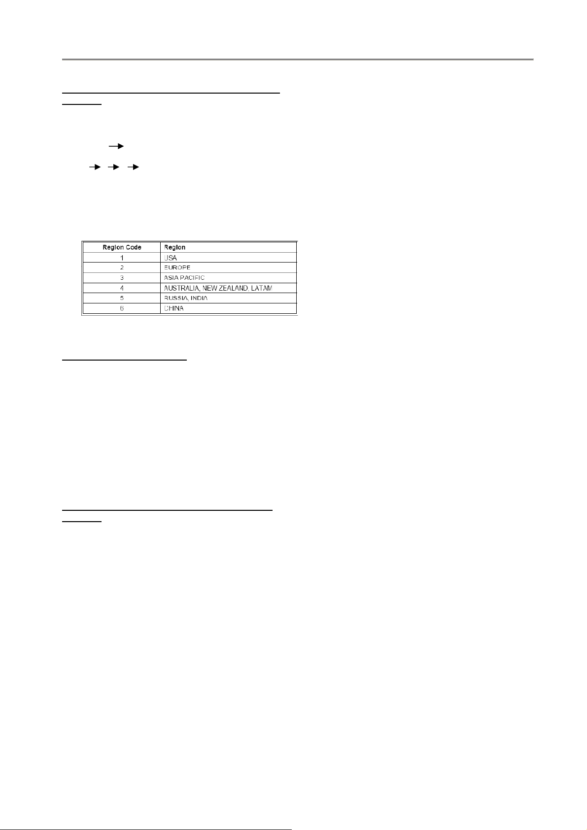
1.2 System, Region Code, etc. Setting Procedure
Procedur
Portable
1. Powe
2. Setup Prefer
3. Press▲(navigation up)or▼(navigation down)
4. Then press OK to confirm your region code.
5. Refer below table for your region code setting
e to change r
r ON the DVD player and do not insert
DISC inside player
Press IR in the sequence as
9 6 5 3
The LCD display showed the existing region
Code
repeatedly to select the number from 0 to 6.
egion code of your DVD
Select “0” setting = Region Free (confidential)
Procedure for SW upgrade
1. The upgrade
re-named: PHILIPS.BIN
2. “PHILIPS.BIN” copy to USB or CD-ROM into
the data;
3. Reading the USB or CD-ROM,in accordance
with prompt,press ”OK” key to upgrade.
Warning: Do not unplug the AC adapter during
firmware upgrade to prevent flash corrupt of
the set!!
Procedure to check SW version of your DVD
Portable
1. OPEN
2. Press SET
3. Select Preferences
4. Select Version Info
5. Press “OK” key
will provide a document
UP MENU
Page 5

2.0 Safety instruction
2-1
1. General
Safety regulations require that during a repair:
. Connect the unit to the mains via an isolation
transformer.
. Replace safety components indicated by the
symbol
Only by components identical to the original ones.
Any
Other component substitution (other than original
type)
May increase risk of fire or electrical shock hazard.
Safety regulations require that after a repair, you
must
Return the unit in its original condition. Pay, in
particular,
Attention to the following points:
. Route the wires/cables correctly, and fix them with
the
mounted cable clamps
. Check the insulation of the mains lead for external
Damage
. Check the electrical DC resistance between the
mains
Plug and the secondary side:
1) Unplug the mains cord, and connect a wire
2) Set the mains switch the “on” position (keep
3) Measure the resistance value between the
4) Repair or correct unit when the resistance
5) Verify this, before you return the unit to the
6) Switch the unit “off”, and remove the wire
safety
between
The two pins of the mains plug.
the
Mains cord unplug).
mains
plug and the front panel, controls, and chassis
bottom.
measurement is less than 1M Ω
customer/user (ref. UL-standard no. 1492).
between
the two pins of the mains plug.
2. Laser safety
This unit employs a laser. Only qualified service
personnel
May remove the cover, or attempt to service this
device
(due to possible eye injury).
Laser device unit
Type :Semiconductor laser GaAIAs
Wavelength :650nm (DVD)
:780nm (VCD/CD)
Output power :7mW(DVD)
:10mW(DVD/CD)
Beam divergence:60 degree
Note: Use of controls or adjustments or
performance of procedure other than those
specified herein, may result in hazardous
radiation exposure. Avoid direct exposure to
beam.
Page 6

3-1
3.0 INSTRUCTION FOR USE
You can download this information from the following websites:
http://www.philips.com/support
http://www.p4c.philips.com
Page 7
4-1
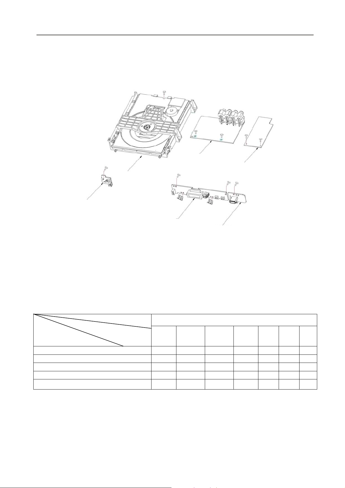
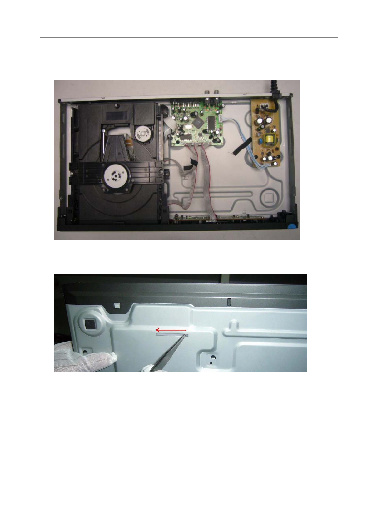
4.0 MECHANICAL AND DISMANTLING INSTRUCTIONS
The following guidelines show how to dismantle the player.
5 screw
Step1: Remove
Step2:If the tray
Step2: If it is necessary
s around the Top Cover, and then remove the Top Cover(Figure1)
Figure 1
can’t open in normal way, you can make it through the instruction as below (Figure2)
Figure 2
to dismantle Loader or Front Panel, the Front door should be removed first(Figure3)
Page 8
4-2
4.0 MECHANICAL AND DISMANTLING INSTRUCTIONS
Figure3
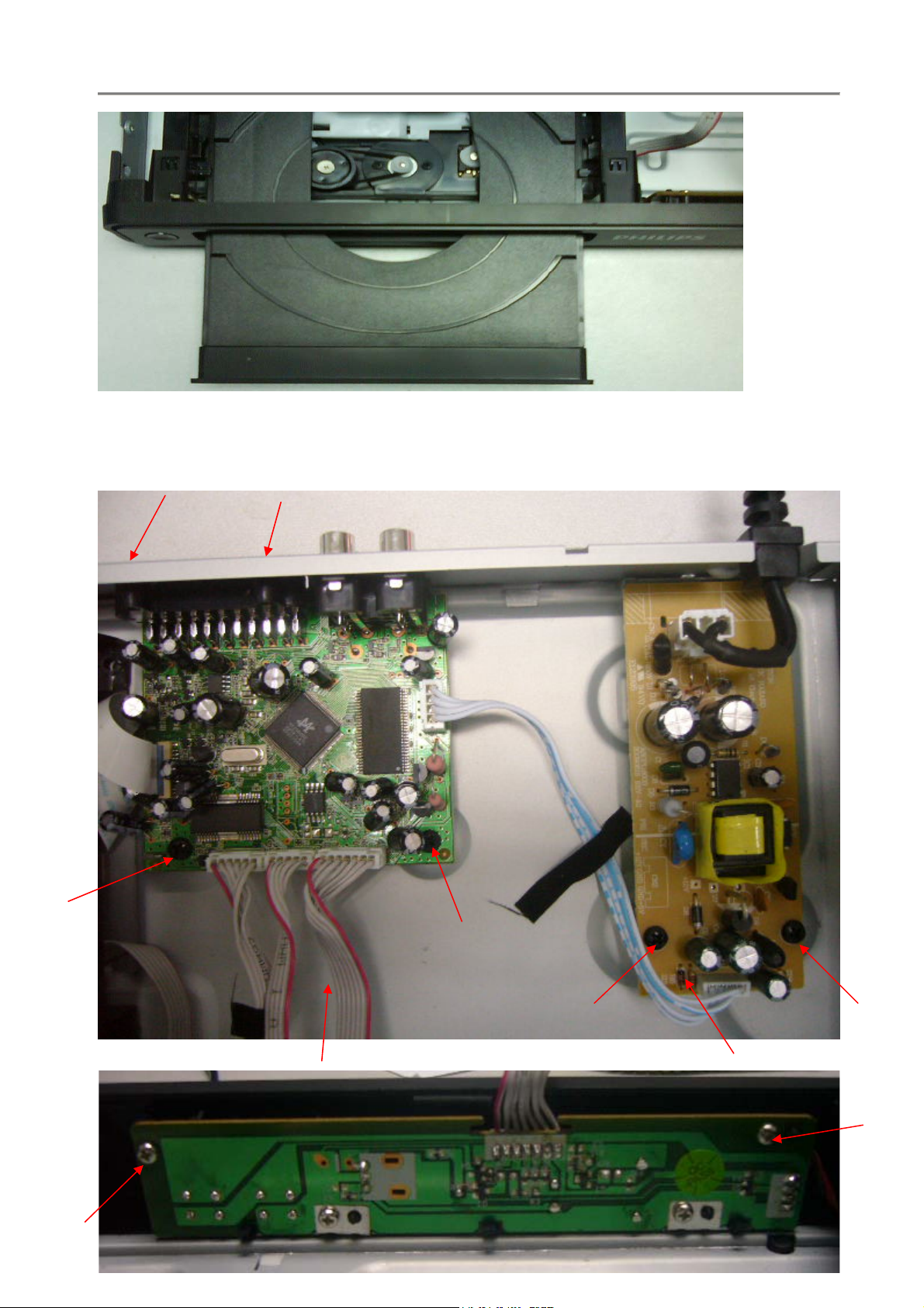
Step4: Remove the 10 scre
ws on board to dismantle the DVD BOARD & POWER BOARD & LED BOARD (Figure 4&5)
Figure4
Page 9
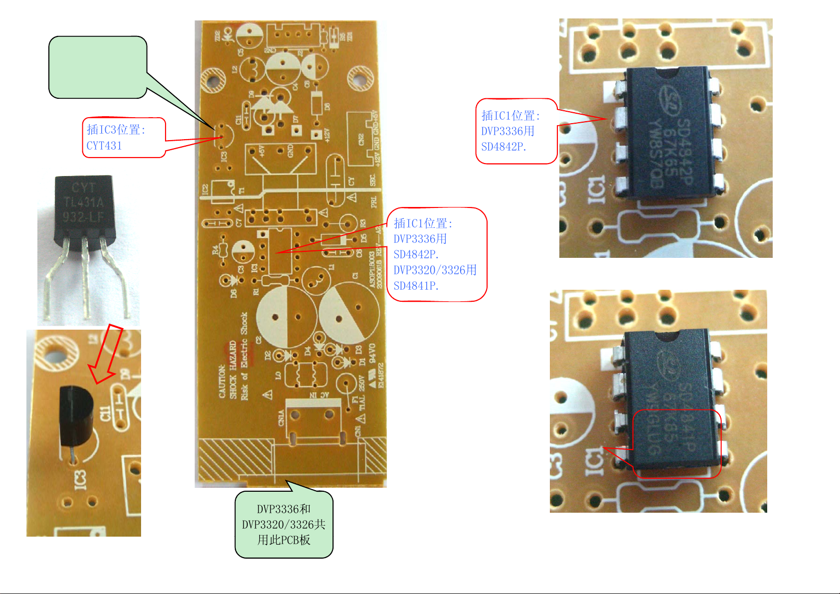
DVP3336和
DVP
3320
/
3326
用
用此
PCB
板
CYT431 location
(IC3)
Common power board of
DVP3336/DVP3320/3326
location IC1:
DVP3336 uses
SD4842P
DVP3320/3326 uses
SD4841P
IC1: placement of
SD4842P on
DVP3336 board
IC1: placement of SD4841P
on DVP3320/3326 board
Power Board repair (swap IC and
transformer)
DVP3320/3326共
用此IC
插IC3位置:
CYT431
插IC1位置:
DVP3336用
SD4842P.
插IC1位置:
DVP3336用
SD4842P.
SD4841P.
插IC1位置:
DVP3320/3326
用SD4841P.
DVP3336和
DVP3320/3326共
Page 10
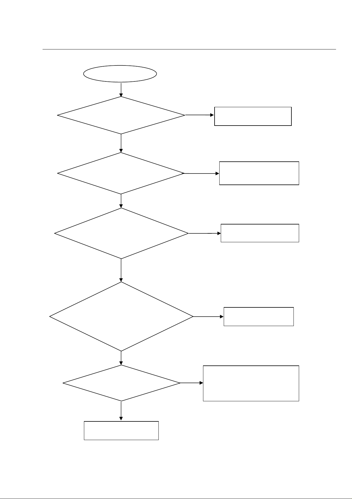
Sp
indle motor does not move
Motor not move
Go
5-1
ouble shooting chart
Tr
Check the FFC connection
between 24P and the loader.
Yes
Check wh
(VCC) voltage is normal.
Check w
(1.9V for CD & 2.3V for DVD)
on L21 & L22
ether “MO_VCC”
Yes
hether laser voltage
Yes
No
No
Correct connection
Check the MOVCC pow
supply
No
Check/Replace Q10ǃQ11.
er
1. Whether voltage on pin 23 of U2
varies between 0 and 3.3V (3.3V
for CD and 0V for DVD),
2. Whether peripheral components
are eroded or badly soldered.
Yes
Check opu focus
Yes
Check/Repl
ace the loader
No
No
1. Check U2 25pin FOO signals
2.If there are F+, F-, T+ and T-
signals output from U1.
Check/ Replac
e U1.
Page 11
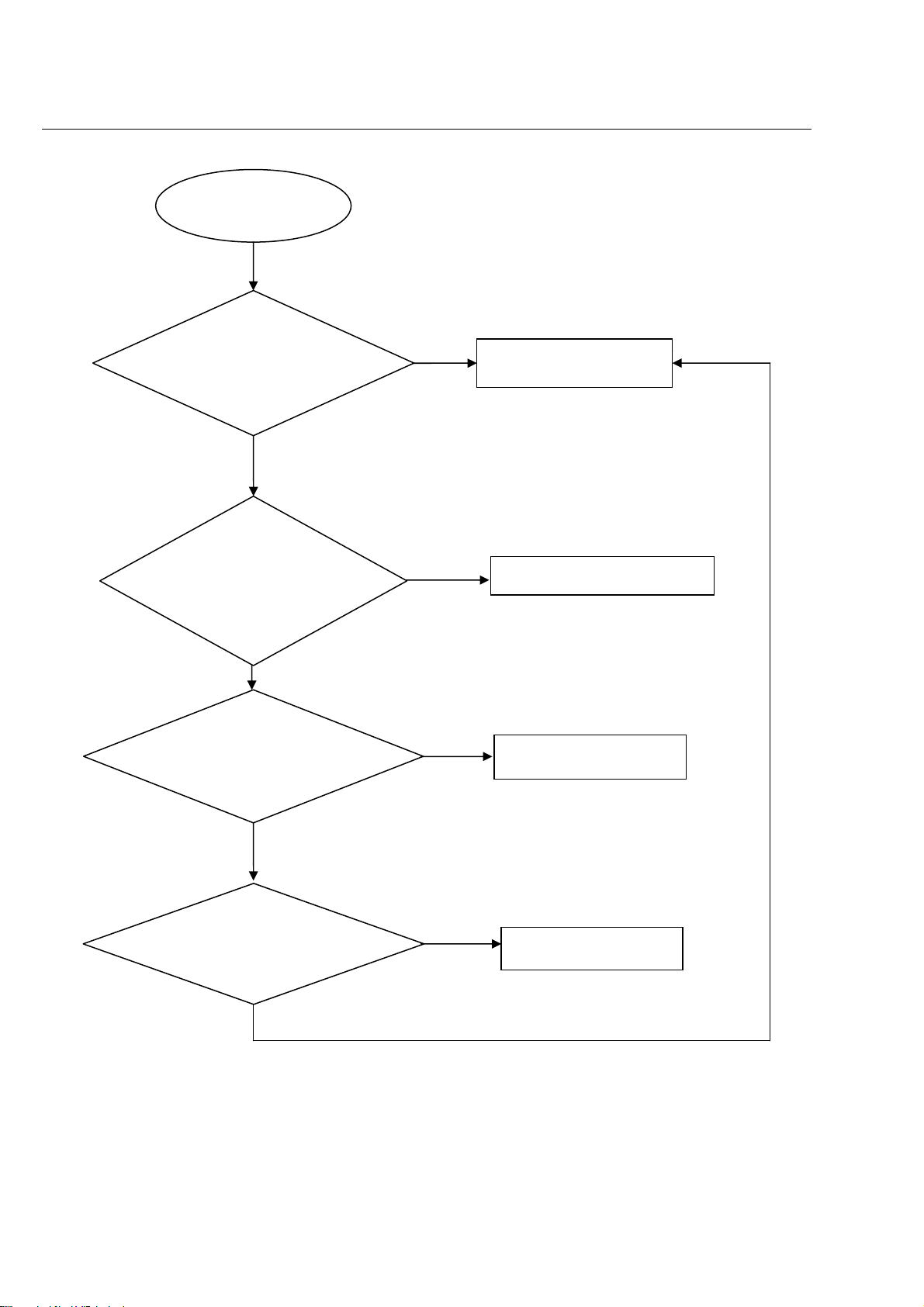
The pow
er can not be on or off
5-2
ouble shooting chart
Tr
The pow
Check the pow
on the power board and the connection to
to decoder board is normal.
Check if the CON2 on the front
board to J 6(7PIN) on the decoder board
is in good contact.
er can’t be
on or off
Go
Yes
er supply
Ye s
No
No
Replace the power boar
or correct the connection
Check/Correct connection
d
Yes
Whether the connection
to Standby Board is br
Yes
Whether there is 0V or
3.3V voltage difference on
Pin41 of U2
Yes
oken.
No
No
Correct the connection
Replace U
1.
Page 12
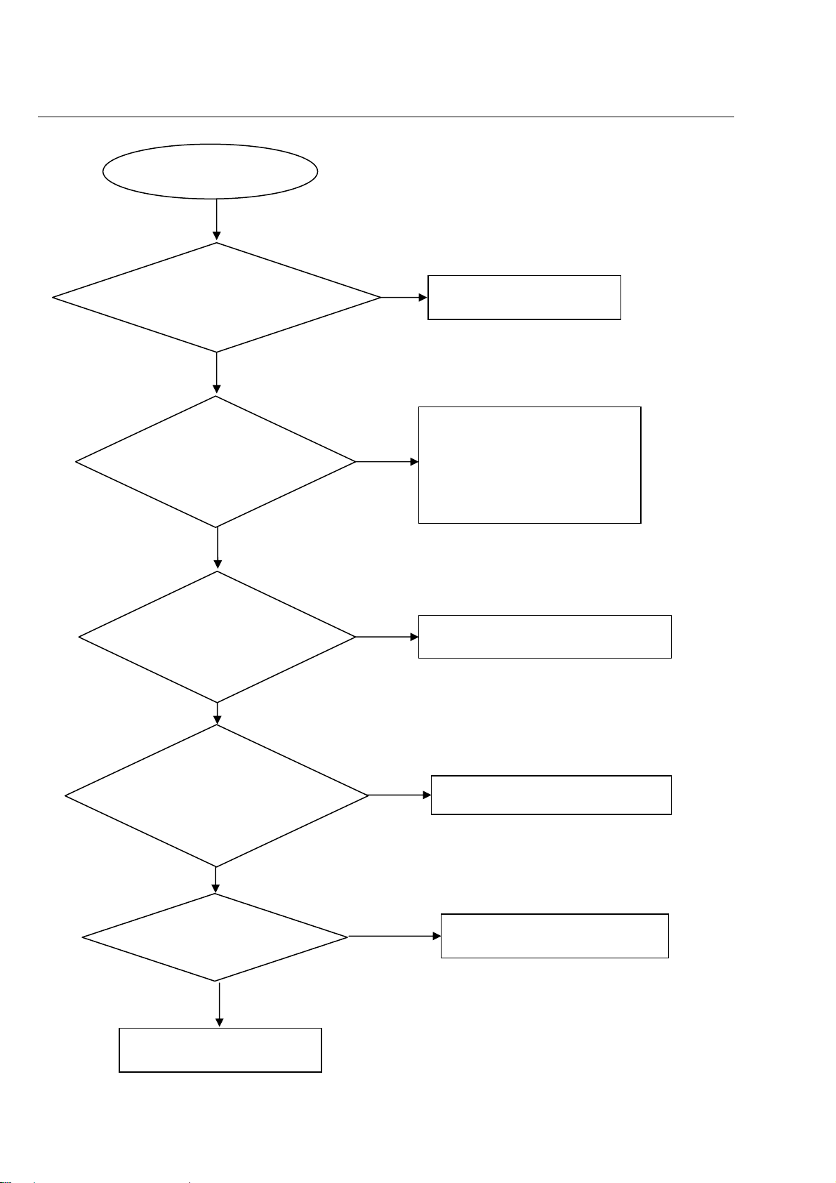
Disc cannot be read
Disc cannot be read.
.
Yes
5-3
ouble shooting chart
Tr
Check the FFC connection
een 24P and the loader.
betw
Yes
Check whether there is
laser voltage (1.9V for CD
and 2.3V for DVD) on
Collector of Q11 &Q10
Yes
Check U1, U2, and
peripheral components are
eroded or badly soldered.
No
No
No
Check the lo
1.Check volt
varies between 0 and 3.3V:
Æ3.3V for CD
Æ0V for DVD
2.Check whether peripheral
components are eroded or defect
Re-solder or replac
aded circuit
age on pin 23 of U2
e the defective parts
Yes
Check if there is RFO signal
on the pin8 of HA1. (The
normal RFO signal is a clear
reticulated wave)
Ye
s
Check the connection
betw
een U2
Yes
Replace U2 or loader
.
No
No
Check U2 and peri
Correct connection
pheral components
Page 13

p
p
p
,
5-4
Only
DVD disc or only disc except DVD can be played
Only DVD disc
exce
t DVD can be Played.
, or only disc
Go
ouble shooting chart
Tr
Check the FFC
co
nnection between
24
in and the loader
Yes
Check laser volt
output on Collector of Q11, if
pin 17 of U2 is at low level.
Yes
Check wh
is voltage variance on
in 18 of U2.
ether there
Yes
.
age (1.9V)
No
No
No
Check the lo
Check the solder st
peripheral components
check if bad solder exist on U2 and
peripher
aded circuit
atus on U2 and
al components
w
Check
pin 125-128 of U2 and peripheral
components are badly
soldered
hether pin 1 - 26 and
defected
Yes
Check Q5, Q6, Q7
ether in good
wh
condition
Yes
Change U2
or the loader.
No
Replace the bad spare parts
No
Correct connection
Page 14

Distorted audio and
loud noise
5-5
ouble shooting chart
Tr
Distorted audi
loud noise
Yes
Check he pow
voltages +12V
to the operation amplifying
L2 are normal
Yes
Check wh
muting transistors Q12,
Q14, are normal
Yes
o and
er supply
ether the
No
Replace L2
No
Replace Q12, Q14
Checking the
the feet has no to break
to open
Yes
Check w
or U2 power supply
normal
Replace U2, U5
hether the U5
Yes
No
U2 leads
No
No
Correct connec
Check U2, U5
tion
Page 15

Abnormal color of video picture
p
5-6
ouble shooting chart
Tr
Abnormal col
video
Yes
Check w
output signal is normal.
Yes
Check w
and 1.8V power supply
voltages on the decoder
board are normal.
hether the 3.3V
Yes
or of
icture
hether the 27MHz
No
No
Check Y
Check other of
circuit
1, R17, C21 and C22
power supply electric
Check wh
video filter network
circuit is normal.
ether the
Yes
Change U2
No
Correct the connection
Page 16

Remote reception is insensitive or fails.
prop
5-7
ouble shooting chart
Tr
Go
Yes
Yes
ception is
rks
erly.
er
Remote re
insensitive or fails.
Check if the remote
control wo
Check if the pow
supply voltage to the
remote censor is normal
No
No
Check battery
Check R1 R2 on front board
Use an oscil
if there is output waveform
from the first pin IR of the
remote censor after pressing
button on the remote control.
Check if there is IR
sign
U2
loscope to check
Yes
al on pin 44 of
No
Correct connection
Ye
No
s
IR1(PIN 3 - RCw
Change U2
aveform
IR w
aveform)
Page 17

No video picture, no sound.
y
No video picture,
no sou
Go
nd.
5-8
ouble shooting chart
Tr
Check whether all the
voltages from the power
board to the decoder board
are normal.
Yes
Check if the reset circuit consisting
of C13, Q4, Q3,R11,R12,R13,R15,R16 is normal
gh level for tens of milliseconds,
(at a hi
then constantl
Check w
27MHz signal output.
Check if there is 128MHz
signal output on R49.
at 0V).
Yes
hether there is
Yes
No
No
No
Check the lo
No
Cry
stal oscillator Y1 and
peripheral components
are defected or eroded.
aded circuit
CVBS(L27 point) w
Change C13,Q4,Q3
Check wh
short-circuit or bad
solder on U3, U4
ether
aveform
27M wa
veform
Yes
Check U3.
SDRAM(R49 SDCLK) waveform
Reconnect the component i
short-circuit
Yes
n
No
Page 18

No display
on LED, and buttons do not work
5-9
ouble shooting chart
Tr
LED an
buttons do not work
Check w
correct contact
between CON1 of front board
and J 6 of decoder board
Check DV33(+3.3V)
volt
and front board
d
Yes
hether there is
s
Ye
age on the power
s
Ye
No
No
Correct co
Fix pow
a power supply for should
electric circuit
er supply board top
nnection
Check whether there is 0V
or 3.3V on the signals of VPLAY,STB
CLK, DATA
Yes
Check whether the circuit
connected to LED & BUTTONS
is broken,
Check wether Q1,Q2,Q3,Q4 for 3904
&LED is broken,
Replace LED or Q1,Q2,Q3,Q4
Yes
No
Check the U2’s pin 33,34,40,41
the J 6 connect condition
No
Correct connection
arrive
Page 19

BLOCK DIAGRAM
6-1
AC 110-220V
POWER BOARD
+5V
SW5888/MOTOR DRIVE&DC-DC
DECK(CMS S76R)
+12V
+1.8V
+3.3V
YD4558
LED
DISPLAY
ANALOG
AUDIO OUT
5.1CH
YD4558 YD4558
ANALOG
AUDIO
5.1CH
MTK1389DE/LA
USB
FLASH
16M
SDRAM
16*16
DVD_L
DVD_R
I2C BUS
+12V
G1445RD1D
FM_L
YD4558
FM_L
SI4702(FM
TUNER)
Y/U/V
COAXIAL
SPEAKER(8ohm/1W)
+5V
FM_R
FM_R
+3.3V
Page 20

CI
RCUIT DIAGRAM-MAIN BOARD (FM)
7-1
DV33
GPIO11
GPIOC2
GPIO21
DV33
L4 FB600R
L0805
GPIO11 [2]
GPIOC2 [2]
GPIO21 [2]
DV33 [1,2,3,4,5]
+
TC1
10uF/16V
GND
Near phonejack(PT-242)
FM
VCC_FM
C108
22nF
FM_RST
R149
15K
GND
If use 3V3D to power the si4702
chip. must use GPIO to controll the
FM reset
TP4
ANT
L32
270nH/0603
C114
470pF
GND
GPIO11
GPIOC2
GND
VCC_FM
C109
1000pF
FM_RST
R57 1K
C5
100P
GND
GPIOC3
CLK
U10
1
NC
2
FMIP
3
RFGND
4
GND
5
RST
R148 10K
R150 10K
SI4702/03
GND
192021
NC
GND
GPIO1
Si4702
QFN20
SEN
SCLK
678910
21
GPIO
C105 22pF
X1
32.768KHz
C106 22pF
GPIOC3
17
18
O2
GPIO3
GPI
IO
SD
RCLK
CLK
16
VA
GND
LOUT
ROUT
GND
VD
VIO
VCC_FM
GND
15
14
13
12
11
Si4702
GND
C113
100nF
C107
GND
22nF
VCC_FM
C110 470
C111 470
GND
GND
P
P
C112
22nF
GND
GND
FMINL
FMINR
VCC_FM
Page 21

CIRCUIT DIAGRA
M-MAIN BOARD(VIDEO)
7-2
V_G
V_R
V_B
R125 0R
3906
C
B
R134 0R
R140 0R
E
R135
75,1%
R141
75,1%
R126
75,1%
L27 1.8uH
C96
100P
L28 1.8uH
C99
P
100
L29 1.8uH
C101
100P
C100
100P
C102
100P
C97
100P
R130
75
2
R136
75
2
R122
75
2
VB_5V
VB_5V
13
VB_5V
13
13
Q23
PMBT
Q26
PMBT
Q27
PMBT
R124 75,1%
3906
R133 75,1%
3906
R138 75,1%
3906
R/V_OUT
B/U_OUT
G/Y_OUT
CVBSO
P47
G/Y_OUT
P45
P48
P44
P43
B/U_OUT
R/V_OUT
Low Impedance Mode
CVBS_OUT
R660
R642
75,1%
75,1%
H-Impedance Mode: R660=7
L-Impedance Mode: R660=75 1%,R642=75
1%.
JK3
6
4
5
3
1
2
AV4-8.4-7D2
C617
100pF
5
1%,R642=NC.
L606
1.8uH
C618
100pF
CE600
22uF/25v
CVBS_OUT
V_R
V_B
V_G
GPIO13
DV33
VCC
GPIO13
R131 470R
VB_5V
R641
3.3K
Q613
R643
3.3K
2
PM
BT3904
R645
75
CE98
+
220uF/10V
1 3
+
DV33
R127 10K
R129
4.7K
2
CVBSO
CVBS_OUT [2]
V_R [2]
V_B [2]
V_G [2]
GPIO13 [2]
DV33 [1,2,3,4]
VCC
Q24 CES2307
[1,2,4]
VB_5V
C98
0.1uF
Q25
PMBT
3904
1 3
V_5VVCC
12
CE44
+
10uF/10V
Page 22

CIRCUIT DIAG RAM-MAIN BOARD (AUDI
R65
C78 100pF
33k
R68
CE24
5.1k
R67
ALS
+
10k
10uF/10V
CE30
R85
ALF
+
10k
10uF/10V
U5A
CE25
-
2
+
3
YD4558 OPA
C80
1000pF
8 4
OP_12V
VREF
R77100k
R81
33k
C82 100pF
R86
U6A
5.1k
-
2
+
3
YD4558 OPA
C84
1000pF
8 4
OP_12V
R96 100k
R69
+
1
1k
10uF/16v
R75
A_MUTE
1k
CE31
R87
+
1
10uF/16v
1k
R94
A_MUTE
VREF
1k
LSCH
R73
100k
Q14
2
4
PMBT390
1 3
CENT
R92
100k
Q18
2
4
PMBT390
1 3
CE26
ARS
10uF/16v
CE32
ARF
10uF/16v
R66
C79 100pF
33k
R71
5.1k
R70
+
10k
C81
1000pF
R88
+
10k
C85
1000pF
U5B
-
6
7
+
5
YD4558 OPA
8 4
OP_12V
R78100k
R83
33k
C83 100pF
R89
5.1k
U6B
-
6
7
+
5
YD4558 OPA
8 4
OP_12V
VREF
R97100k
7-3
O)
AR
AR
AL [2]
ARS [2]
ALS [2]
ARF
ALF [2]
ASPDIF [2]
AUDIO_MUTE [2]
VCC [1]
+12V [1,6]
DV33 [1,2,3]
FMINR [6]
FMINL [6]
[2]
[2]
AL
ARS
ALS
ARF
VCC
CE27
R72
+
1k
10uF/16v
R76
A_MUTE
A_MUTE
CE33
10uF/16v
2
1k
R90
+
1k
R95
2
1k
VREF
RSCH
R74
100k
Q15
PMBT390
4
1 3
MU
SUB
R93
100k
Q19
4
PMBT390
1 3
DV33
AUDIO_MUTE
TE_Circuit
R91 1K
R79
3.3k
R80 10K
R84
NC
R663 22K
Q615 PMBT39
06
3
1
2
Q614 PMBT39
06
3
R661 4.7K
1
12
+
CE28
2
220uF/10V
R662
4.7k
Q17
2
PMBT390
4
1 3
R82 100
A_MUTE
ALF
ASPDIF
AUDIO_MUTE
VCC
+12V
DV33
FMINR
FMINL
AR
FMINR
CE39 10uF/16v
AL
FMINL
CE40
10uF/16v
CE35
10uF/16v
R98 100
ASPDIF
FB600R
L26
+12V
L0805
EC2
22uF/25V
R114 51K
R117 51K
CAP5/5.0A
R0402
R0402
CE34
12
+
10uF/16v
12
+
R109 20K
12
+
R110 6.2K
12
+
R100 56K
R101
20K
R102
6.2K
C92
1000pF
R108 56K
R111
5.1K
C88 82pF
R103
5.1K
C89
1000pF
C90 82pF
6
5
R118 100K
-
+
8 4
-
2
+
3
8 4
R107 100K
U7B
7
YD4558 OPA
OP_12V
VREF
U7A
YD4558 OPA
OP_12V
CE36
R104
+
1
1K
10uF/16V
R34 1K
A_MUTE
VREF
CE41
R112
+
1K
10uF/16V
R55 1K
A_MUTE
2
PMBT390
1 3
RCH
Q20
R106
2
100K
PMBT3904
1 3
CE38
12
+
0R
LCH
R116
Q21
4
100K
CE43
12
+
0R
U9A
CE37
-
2
+
3
8 4
-
6
+
5
8 4
YD4558 OPA
OP_12V
U9B
YD4558 OPA
OP_12V
VR_R_IN
+
1
10uF/16V
CE42
+
VR_L_IN
7
10uF/16V
56K
+
FM_AUDIO/OUT
OP_12V
R120
R0402
C94
R121
0.1uF
56K
C0402
R0402
VREF
+
C95
EC3
0.1uF
47uF/16V
C0402
CAP5/5.0A
R48 39K R0402
U8A
C13 1uF
FM_AUDIO/IN
A_MUTE
R47 5.6K R0402
R115 5.6KR0402
C22
1uF
R664
2
PMBT3904
1k
1 3
4 5
+
3
BYPASS
2
C93
1UF
Q616
Shutdown
1
G1445RD1D
R41 39K R0402
R37
10K
R0402
DV33
AMP_CONTROL is High ,The G1445 will be shutdown
OPTICAL+COAXIAL
EC1
100uF/10V
CAP5/5.0A
+
SPEAKER+
SPEAKER-
L25
C91
0.1U
6
8
7
BIAS
C86
COAXIAL
0.1uF
R99
100K
C87
330pF
J7
1
FM_AUDIO/IN
P32
P30
FB600R
VCC
L0805
P34
P33
J5
SPEAKER+
2
SPEAKER-
1
2P/1.25MM
P42
P41
P40
P39
FM_AUDIO/OUT
COAXIAL
LCH
RCH
2
3
3P/2.0MM
JK2
6
4
5
3
1
2
AV3-8.4-7D
LSCH
P38
RSCH
P37
CENT
P36
SUB
P35
JK1
6
4
5
3
1
2
AV4-8.4-7D1
Page 23

CIRCUI
T DIAGRAM-MAIN BOARD (SDRAM)
7-4
S-FLASH
DV33
R62 10k
R63 10k C74
SF_CS
SF_DO
U4
1
CE#
VDD
2
SO
HOLD#
3
WP#
SCK
4 5
VSS SI
EN25F16-100HCP
8M/16M bit
SF_CS
SD33
DCLK
BA0
BA1
RAS#
CAS#
WE#
8
7
6
R64 NC
SF_CK
SF_DI
R53
R54 10k
R21 33
DV33
10k
DV33
SDCKE
DCS#
SDCLK
R61 10k
C77
0.1uF
SDRAM (Dual Layout)
MA0
MA
MA2
MA4
MA5
MA6
MA7
MA8
MA9
MA10
MA11
BA0
BA1
SDCLK
SDCKE
DCS#
RAS#
CAS#
WE#
DQM0
DQM1
DV33
23
1
24
25
26
29
30
31
32
33
34
22
35
20
21
38
37
19
18
17
16
15
39
36
40
54
41
28
U3
A0
A1
A2
A3
A4
A5
A6
A7
A8
A9
A10/AP
A11
BA0/A13
BA1/A12
CLK
CKE
CS
RAS
CAS
WE
DQML
DQMH
NC
NC
VSS
VSS
VSS
WINBOND W9864G6XH-6
DQ0
DQ1
DQ2
DQ3
DQ4
DQ5
DQ6
DQ7
DQ8
DQ9
DQ10
DQ11
DQ12
DQ13
DQ14
DQ15
VCC
VCC
VCC
VCCQ
VCCQ
VCCQ
VCCQ
VSSQ
VSSQ
VSSQ
VSSQ
2
4
5
7
8
10
11
13
42
44
45
47
48
50
51
53
1
14
27
3
9
43
49
6
12
46
52
SD33
SD33
DQ0
DQ1
DQ2
DQ3MA3
DQ4
DQ5
DQ6
DQ7
DQ8
DQ9
DQ10
DQ11
DQ12
DQ13
DQ14
DQ15
DQ[0..15]
MA[0..11]
DQM[0..1]
BA[0..1]
DCLK
RAS#
CAS#
WE#
MA[0..11] [2]
DQM[0..1] [2]
BA[0..1] [2]
DCLK [2]
RAS# [2]
CAS# [2]
WE# [2]
DRAM I/F
SF_CK
SF_CS
SF_DI
SF_DO
SF_CK [2]
SF_CS
SF_DI [2]
SF_DO [2]
S-FLASH
DV33
DV33 [1,2,4,5]
POWER
DV33 SD33
L24 FB600R
SD33
C72
0.01uF
C73
1000P
CE23
+
100uF/10v
0.1uF
C75
0.01uF
C70
1000P
C76
1000P
DQ[0..15] [2]
[2]
C71
0.01uF
Page 24

CIRCUIT DIAGRAM-MTK1389DE/LA
7-5
DV33
1
2
3
4
5
6
7
8
9
10
11
12
13
14
15
16
17
18
19
20
21
22
23
24
SONY KHM31
1
FOSO
TRS
FMSO
DMSO
R18 10k
SP-
0R/0603
R22
SP-A
D2
2
G
1
3E
2SK3018
FF+
T+
TC/c
D/d
CD/DVD SW
RF
A/a
B/b
F
GND-PD
Vc(Vref)
Vcc
_1
E
NC
VR-CD
2SK3018
VR-DVD
CD-LD
MD
HFM
NC
DVD-LD
GND-LD
3
HA1
24
LD-DVD
23
22
AVCC1
21
MDI1
20
LD-CD
19
VR-DVD
18
VR-CD
17
16
E
15
AVCC1
14
V20
13
12
F
11
B
10
TOP
A
9
RFO
8
IOA
7
D
6
C
5
T-
4
T+
3
F+
2
F-
1
HEADER 24 SMD0.5 TOP
O
C56
C57
C55
330pF
0.1uF
330pF
C64
C65
C63
0.01uF
1000P
0.01uF
Chip Decap.
P13
P49
P50
P51
P52
R19 10k
R20
1R/0603
R23 10k
S
R25 100k
2
Q6
R30
0R
P24
P25
P26
C52 0.1uF
P19
P58
P22
P10
P17
R49 27k
R50 27k
R51 15k
R52 10k
C58
0.015uF
1
B
2SB1132
13
13
_3
_2
P23
P27
P8
P18
P9
P16
V1889L_3V3
C31
0.1uF
R31
0R
C67
0.01uF
SP-A
SP+
LIMIT
SLSL
C
C
1 3
2
Q7
2SK3018
P20
+
C35
0.1uF
3
E
Q5
M
P
_4
P21
10uH
V1P4
6P/2.0MM
1
2N3904
R26 10k
R27 10k
2
BT3904
R28 100k
CE17
100uF/10v
P28
L22
FOO
TRO
FMO
DMO
C68
0.1uF
J2
1
2
3
4
5
6
OP-
1
D1
BAT54C
2
OP
+
C
3
B
+
Very Important to
reduce Noise
P29
L23
10uH
Q10
2
STS8550D
1 3
R43 4.7
R45 4.7
13
Q13
2
STS8550D
DV33
3
L18 FB600R
AR
ARS
116
115
AVCM
AR / GPIO0
V1.0
DQ1
DQ0
ARS / GPIO
RD1
ARF
113
114
ARF / GPIO
RD2
DQ2
DQ3
VPLAY
VSCK
VSDA
VS
CE10
+
10uF/10v
0.1uF
C30
C36 1500pF
APLLVDD3
111
110
112
APLLCAP
ADACVSS2
ADACVSS1
RD3
RD4
DVDD33
DQ5
DQ4
TB
+
AADVDD
109
APLLVDD
RD5
DQ6
DV33
14 100uF/10v
CE
GPIO21
1K
R58
GPIO20
108
107
AADVDD
AKIN1 / GPIO21 / Audio_Mute
RD6
RD7
DQ7
V1889L_3V3
ADVCM / GPIO20
DVDD18
L10 FB600R
89L_3V3
100p
C4
V_R
V_G
V_B
19
DACVDD3
DACVDD3
GPIO
106
105
104
103
102
101
1009998
B
R
G
AADVSS
DACVDDA
DACVDDB
AKIN2 / GPIO19 / Audio_Mute
DQM0
RD15
RD14
RD13
RD12
RD11
DVSS33
DQ13
DQ12
DQ14
DQ15
DQ11
DQM0
APLLVDD3
thrice resonance
crystal need add
L15 NC/2.7uH
C23
NC/1000pF
TestPoint & Resistor
must reserve.
R24
FS
560
CVBS_OUT
97
FS
CVBS
DACVSSC
VREF
DACVDDC
GPIO13
SPDIF / GPIO12
GPIO11
GPIO10
DVDD18
GPIO9
GPIO8
GPIO7 / CKE
RA3
RA2
DVDD33V14
RA1
RA0
RA10
BA1
DVSS18
BA0
RAS#
CAS#
RWE#
RA4
RA5
RA6
RA7
RA8
RA9
DVDD33
RA11
RCLK
DQM1
RD10
RD9
RD8
MT1389DE/LA/SMD
DQ10
DQ8
DQ9
UP1_7 GPIOC2
P1
XI
C24
27pF
89L_3V3
VREF1
96
89L_3V3
95
GPIO13
94
GPIO12
93
92
GPIO10
91
90
GPIO9
89
GPIO8
88
USB_EN
87
MA3
86
MA2
85
8413
MA1
83
MA0
82
10
MA
81
BA1
80
79
BA0
78
RAS#
77
CAS#
76
WE#
75
MA4
74
MA5
73
MA6
72
MA7
71
MA8
70
MA9
69
68
MA11
67
DCLK
66
DQM1
65
GPIO19
GPIO6 TRCLOSE
P31
P11
R17 100k
Hz
Y1 27M
C40 0.1uF
C9 100P
R56 1K
IOA
LIMIT
XO
C25
27pF
GPIO12 ASPDIF
GPIO11
V18
AUDIO_MUTE
TROPENGPO_B
TROUTGPIO8
DQ[0..15]
MA[0..11]
DQM[0..1]
BA[0..1]
DCLK
RAS#
CAS#
WE#
DRAM I/F
SF_CK
SF_CS
SF_DI
SF_DO
S-FLASH
AUDIO_MUTE
ASPDIF
ARF
ALF
ARS
ALS
AUDIO I/F
GPIO13
CVBS_OUT
V_R
V_B
V_G
VIDEO I/F
STBY
TROPEN
TRCLOSE
TRIN
TROUT
+12
V
TT+
FF+
SL-
+
SL
SP-
SP+
FOSO
TRSO
FMSO
DMSO
V1P4
SERVO I/F
URST#
DV33
VCC
89L_3V3
V18
RFV33
MIX
GPIOC2
GPIO21
GPIO11
AL
AR
DQ[0..15]
MA[0..11] [3]
DQM[0..1] [3]
BA[0..1] [3]
DCLK [3]
RAS# [3]
CAS# [3]
WE# [3]
SF_CK
SF_CS [3]
SF_DI [3]
SF_DO [3]
AUDIO_MUTE [4]
ASPDIF [4]
ARF [4]
ALF [4]
ARS [4]
ALS [4]
GPIO13 [5]
CVBS_OUT [5]
V_R [5]
V_B [5]
V_G [5]
STBY [1]
TROPEN [1]
TRCLOSE [1]
TRIN [1]
TROUT [1]
+12V [1]
T- [1]
T+ [1]
FF+ [1]
SL- [1]
SL+ [1]
SP- [1]
SP+ [1]
FOSO [1]
TRSO [1]
FMSO [1]
DMSO
V1P4 [1]
URST# [1]
DV33 [1,3,4,5]
VCC [1,4]
89L_3V3 [1]
V18 [1]
RFV33 [1]
GPIOC2 [6]
GPIO21 [6]
GPIO11 [6]
AL [4]
AR [4]
[3]
[3]
[1]
[1]
V18
V18 RFV18-1
L11 FB600
V18
1000P
C16
C17 0.1uF
89L_3V3
89L_3V3
C18
10uF/10V
C21
L9 FB600R
L13 FB600R
C20
0.1uF
ADACVDD
C19
0.1uF
DACVDD3DACVDD3
0.1uF
SERVO RF DeCAP.
+
CE11
0.1uF
47uF/16v
+
CE12
10uF/10v
V1P4
P59
V20
C26
RF Reference
MDI1 MDI2
L17 10uH
1 2
10uF/10V
10K
R32
R33
4.7K
2
J3
1
2
3
4
NC/4P/1.25MM
RXD
D
TX
P7
P6
C41
+
CE16
0.1uF
Q8
USB5V
CES2307
Q9
PMBT3904
1 3
F1 0.5A/6V
USB5V
IOA
Only for MT1389L
VCC
C42
0.1uF
USB_EN
VCC
VCC_3V3
R35 470R
close to USB connector
GPIO9
GPIO10
LDO2
RFV33
LDO1
DV33
RxD
TxD
+
CE19
47uF/16v
CE20
+
47uF/16v
RS-232
DV33
L16 FB600R
C28
6800pF
J6
C47
1000P
C50
10uF/10v
R44 0R
C34 10uF/10v
C37 0.1uF
R29 15k
AVDD33
C44
0.01uF
R36 5.1k
C51
0.1uF
STBY
VR-CD
GPO_B
VR-DVD
USB_DP
USB_DM
P5
REXT
TRAY-OPEN
VREF1
TRAY-CLOSE
89L_3V3
L19 FB600
89L_3V3
V18
GPIO20
4
3
2
1
4P/2.0MM
R38 NC
R39 0R
R40 NC
R42 NC
R46 NC
MT1389L&MT1389LA
GPIO3
UP1_6
UP1_7
GPIO4
P56
P53
P54
P4
P55
P3
P2
VCC
DV33
IR
VSDA
VSCK
VSTB
GND
VPLAY
J4
1
2
3
4
5
6
7
8
8P/2.0MM
AADVDD
CE13
+
470uF/10v
C
B
A
D
F
E
V18
89L_3V3
XI
XO
V20
V1P4
T
REX
MDI1
MDI2
LDO1
LDO2
DM
O
FMO
TRAY-OPEN
TRAY-CLOSE
TRO
FOO
TRIN
USB_DP
USB_DM
USB_V33
USB_V18
0.1uF
CE15470uF/
+
C29
10v
10uF/10v
RFO
C38
1uF
OP-
OP+
128
127
U2
INP
1
RFA
RFG / OP
RFH / OPINN
2
RFB
3
RFC
4
RFD
5
RFE
6
RFF
7
AVDD18
8
AVDD33
9
XTALI
10
XTALO
11
AGND
12
V20
14
REXT
15
MDI1
16
MDI2
17
LDO1
18
LDO2
19
AVDD33
20
DMO
21
FMO
22
TRAY_OPEN
23
TRAY_CLOSE
24
TRO
25
FOO
26
FG / GPIO2
27
USB_DP
28
USB_DM
29
USB_V33
30
USB_GND
31
PAD_VRT
32
USB_V18
/ INT#
GPIO4
GPIO3
33343637383940414243444546474849515253505556575458596162636064
3
GPIO4
GPIO
C59
100pF
C33
220pF
C39
AVCM
ADACVDD
AL
ALS
ALF
RFV18-1
126
125
124
123
118
117
122
121
120
119
RFIP
AVDD18
F / GPIO
AGND18
AL / GPIO1
AL
ALS / GPIO
ADACVDD2
ADACVDD1
RFIN / OPOUT
MT1389DE/LA
LQFP-128
Desktop
SF_CS_
SF_DO
SF_DI
SF_CK
UP1_6 / SCL
UP1_7 / SDA
ICE
PRST#IRRD0
GPIO6
35
SF_CK
UP1_7
UP1_6
GPIO6
IR
URST#
SF_DI
SF_DO
SF_CS
C61
C62
C60
100pF
100pF
100pF
Page 25

CIRCUIT DIAGRAM-POWER
& MOTOR DRIVER
BT3904
C8
0.1uF
+12V
RFV33
C11
0.1uF
Desktop Model
RESET Circ
R2
22k
Q2
2
BT3904
PM
1 3
CON1
1
2
3
4
4P/2.54MM
+12V
RFV33DV33
u
it
URST#
12
+
C1
47uF/10v
CO
MMON1389L/K_HM313_AM5888_V6
MT1389L/K (LQFP128)
DVD TEST Board w/ Sanyo HD6x Series PUHs
1 INDEX & POWER, RESET
2 MT1389L/K LQFP128
3 SDRAM & FLASH
4 AUDIO I/F
5 VIDEO I/F
6 FM
DV33
R1
10k
Q1
2
PM
1 3
VCC
GND
+P12V
P57
CE5
+
100uF/16v
CE7
+
47uF/16v
+P12V
R3
15k
R5
4.7k
R4
3.9k
VCC
+P12V
L3 FB600
L6 FB600
7-6
MT1389L/K Full Function:
(USB,1CH MIC,6CH DAC,VGA/SCART,GAME,CARD,VFD)
MT1389L/K General GPIO List
Name
GPIO3
GPIO4
GPIO6
GPIO7
GPO_A
GPO_B
GPIO2
GPIO8
GPIO9
GPIO10
GPIO11
GPIO12
GPIO13 94
GPIO19
GPIO20
GPIO21
GPIOK0
GPIOK1
GPIOK2
UP1_6
UP1_7
ARF
ARS
ALS
ALF
C2
1uF
VCC
0.1uF
C12
PIN
33
34
35
87
22
23
26
88
89
91
92
93
106
107
108
27
28
31
40
41
114
115
119
120
V33
Features
L1 FB600R
L2 FB600R
2
R11
10
OUT18
2
R16
10
OUT33
TROUT
SD_CLK
SD_CMD
HSYNC
VSYNC
AUDIO_MUTE
CE1
+
220uF/10v
+
12
+
CE4
220uF/10v
12
+
CE8
220uF/10v
LIMIT V5_
TRCLOSE
MS_CLK
STBY
TROPEN IOA
TRIN
MS_BS
MS_D0
SD_D0
SCART1
ASPDIF
VSTB
SCART2
ADVCM
AKIN1
USB_DP
USB_DM
PAD_VRT
VSCK
VSDA
AUDIO_ARF
AUDIO_ARS
AUDIO_ALS
AUDIO_ALF
Q3 STS8550D
1 3
R10
5.6R/DIP
R14 2.2R/DIP
Q4 STS8550D
1 3
VCC_3V3
CE2
220uF/10v
L5 FB600R
Rev
The original released.
V1
Base on 3-SYHI89LSD1-V10.D
V2 2007/01/221),Re-arrange MT1389LK Servo IO Pin & VFD P
2),Update brake ciucuit;
3),Change RFO circuit
V3_
1),Re-arrange MT1389L IO Pin
Ext
2),GPIO Extension Solution;
3),Add Scart Circuit;
V4_
1),Exchange Trin and Limit GPIO Pin; 2007/02/12
Ext
1),Modify Mute Circuit; 2007/03/01
Ext
V6 1),Re-arrange MT1389L IO Pin; 2007/06/05
2),Add GPIO reuse function and circuit;
C27
0.01uF
DV33
R7
5.1K/1%
R9
10K/1%
R13
15K/1%
R15
9.1K/1%
FB33
FB18
89L_3V3
DV33
FF+
T-
15
T+
FMSO
OUT18
TRSO
V1P4
STBY
C14
0.1uF
C6
0.1uF
C15
0.1uF
16
17
18
19
20
21
22
23
24
25
26
27
28
MO_VCC
SL+
SL-
MO_VCC
C32
0.1uF
R8
10k/0603
VCC
L8 FB
L7
FB600R
C3
0.1uF
V18
0.1uF
C7
V33
U1
VOTK+
VOTKVOLD+
VOLDVCC2
NC
VCTL
GND
VINLD
NC
TRB2
VINTK
BIAS
MUTE
SW5888
+
CE9
47uF/16v
History
SN
VOFC+
VOFCVOSLVOSL+
VOTR+
VOTR-
VCC
G1G2
REV
FWD
REGO1
VINSL+
REGO2
TRB1
VINFC
DV33
C10 0.1uF
R12 10k/0603
Date
2006/12/12
in;
2007/02/05
+12V
VCC
DV33
89L_3V3
RFV33
V18
URST#
POWER I/F
TRIN
TROUT
TROPEN
TRCLOSE
FOSO
DMSO
FMSO
TRSO
SL+
SLSP+
SPT+
TF+
FV1P4
STBY
+12V [2,4]
VCC [2,4]
DV33 [2,3,4,5,6]
89L_3V3 [2]
RFV33 [2]
V18 [2]
URST# [2]
TRIN [2]
TROUT [2]
TROPEN [2]
TRCLOSE [2]
FOSO [2]
DMSO [2]
FMSO [2]
TRSO [2]
SL+ [2]
SL- [2]
SP+ [2]
SP- [2]
T+ [2]
T- [2]
F+ [2]
F- [2]
V1P4 [2]
STBY [2]
SERVO I/F
14
13
SP-
12
SP+
11
LOAD+
10
LOAD-
9
8
2930
TROPEN
7
TRCLOSE
6
5
4
FB18
3
OUT33
2
FOSO
1
LOADLOAD+
TROUT
TRIN
LOAD-
LOAD+
TRIN
FB33
J1
1
2
3
4
5
5P/2.0MM
P15
P14
P12
MO_VCC
R6 10k/0603
DMSO
Page 26

CIRCUIT DIAGRAM-LED DISPLAY
VCC
CE2
100uF/
12
6.3v
+
R20 100R
DATA
CLK
R21 100R
R22 100R
S
TB D_STB
C4
100pF
D_DATA
D_CLK
R16
10K
R17
10K
VCC
R18
10K
R19
51K
10
11
12
13
14
1
2
3
4
5
6
7
8
9
U1
INT
DI/O
CLK
STB
KEY1
KEY2
Vdd
Seg1/KS1
Seg2/Ks2
Seg3/Ks3
Seg4/Ks4
Seg5/Ks5
Seg6/Ks6
Seg7/Ks7
SM1628
GND
Grid1
Grid2
GND
Grid3
Grid4
GND
VDD
Seg14/Grid5
Seg13/Grid6
Seg12/Grid7
Seg10/Ks10
Seg9/Ks9
Seg8/Ks8
7-7
3.3V
R1
CE3
47uF/
10v
IR_VCC
12
+
21
R2
100R
21
CE1
4.7UF/6.3V
IR/VFD
R3
J2
VCC
3.3V
IR
DATA
CLK
STB
GND
28
27
26
25
24
23
22
21
20
19
18
17
16
15
C5
100pF
1
2
3
4
5
6
7
8
6x1 W/HOUSING
CON7-2.0MM
LED-
VCC
R23
LED+
1 2
51K
D1
510
67431
IR
10K
2
REM301
C1
100pF
4
5
231
KS3 OPEN/CLOSE
1 2
43
KS4 Play/Pause
1 2
3 4
LED+
LED-
STB-
STB+
CON3
1
2
3
4x1 W/HOUSING
4
CON4A-2.0MM
8
9
111213
7-Sement
DIS PLAY
Page 27

CIRCUIT DIAGRAM-USB JACK
7-8
USB_5V
USB_5V
USB_DM
USB_DP
GND
CE1
+
100uF/10v
1
2
3
4
5
6
J2
USB2.0
AUDIO_IN
AUDIO_OUT
P1
3 4
P2
P3
P4
P5
P6
21
VR1
10K
5
VR-B10K
USB_5V
USB_DM
USB_DP
AUDIO_OUT
AUDIO_IN
J1
1
2
3
4
5
6
7
7P2.0
Page 28

7-9
MAIN TOP PCB
Page 29

7-10
MAIN BOTTOM PCB
Page 30

7-11
LED DISPLAY TOP PCB
Page 31

7-12
LED DISPLAY BOTTOM PCB
Page 32

7-13
USB TOP PCB
Page 33

7-14
USB BOTTOM PCB
Page 34

7-15
LED TOP PCB
Page 35

7-16
LED BOTTOM PCB
Page 36

8-1
8.0 Exploded View Diagram
Page 37

DVP3336/94 MAIN PCB PARTS LIST
JK2
996510028076
AV JACK AV38.47D
1
No 12NC No. Part Name Qty
1 996510028058 DVD PCBA ASS'Y DVP3336 1
L32 996510028046 IC MT1389DE/LA LQFP128 CODEC 1
U2 996510028038 IC SI4702C19GM QFN20 RADIO 1
U10 996510028069 IC G1445RD1D TDFN3X38 AMP 1
U8 996510028064 IC SW5888 BTL DRIVE SW 1
U1,U6,U7,U9 996510028051 IC YD4558PIN XY 4
U3 996510028043 IC W9864G6XH6 64M SDRAM 1
U4 996510028054 IC EN25F16100HIP 16M FLASH 1
Q3,Q4,Q10,Q13 996510028047 TR STS8550D TO92 PNP 4
X1 996510028039 X'TAL 32.768KHZ +/10PPM 1
Y1 996510028074 X'TAL 27.00MHZ +/10PPM 1
Q6,Q7 996510028056 TR 2SK3018 SOT23 2
Q8,Q24 996510028041 MOS CES2307 SOT23 CET 2
Q1,Q2,Q5,Q9,Q14
,Q15,Q17,Q18,Q1
9,Q21,Q20,Q25,Q
613,Q616
Q23,Q26,Q27,Q61
4,Q615
D1 996510028055 DIODE BAT54C SOT23 1
JK1,JK3 996510028087 AV JACK AV48.47D1 2
996510028078 TR PMBT3904 SOT23 NPN 14
996510028086 TR PMBT3906 SOT23 PNP 5
F1 996510028048 CHIP RESET FUSE 0.5A/6V LPNSM050 GP 1
DVP3336/94 USB PCB PARTS LIST
No 12NC No. Part Name Qty
2 996510028085 USB PCB ASS'Y DVD3336 1
VR1 996510028088
J2 996510028079 DIP USB AF180°USB015 ZIYOUDA 1
DIP VR B10K 18/2(BLACK)HDS
DVP3336/94 STANDBY PCB PARTS LIST
No 12NC No. Part Name Qty
3 996510028049 STANDBY PCB ASS'Y DVD3320 1
KS5 996510028072 TACT SWITCH 6x6x5mm 180g JIXIN 1
LED3 996510028067 LED RED 1.8V D3 MASON 1
DVP3336/94 LED PCB PARTS LIST
No 12NC No. Part Name Qty
4 996510028068 LED DISPLAG PCBA ASS'Y DVP3320 1
U1 996510028075 SMD IC SM1628C SOP28 DRIVER SUNMOON 1
D1 996510028044 DISPLAY LED DT25801BG DL 1
R1 996510028082 DIP IR SENSOR 36KHZ IRM36C AAD 1
KS3,KS4 996510028072 TACT SWITCH 6x6x5mm 180g JIXIN 2
1
DVP3336/94 POWER PCB PART LIST
No 12NC No. Part Name Qty
5 996510028066 12W/2P OPEN FIXED 94VERSION PCBA 1
Page 38

DVP3336/94 DECK PARTS LIST
No 12NC No. Part Name Qty
7 996510028053 DVD DECK CMS-S76R IM 1
6 996510028059 DVD LOADER WXD8829B ASA 1
DVP3336/94 ACCESSORIES PARTS LIST
No 12NC No. Part Name Qty
9 996510028063 FFC 24P/0.5MM 220MM(3/54/8) +/+OU 1
12 996510028052 R/C CD31A006 BLACK C&D DVP3336/94 1
14 996510028081 AC CORD VDE 94FIXED 1.3M HO3VVH2F 1
15 996510028065 AV CORD RCA/M*3/1.3M BOTH ENDS YI 1
1
7 996510028045 SPEAKER 8 OHM 0.7W Φ40 SHUNJIA 1
DVP3336/94 MECHANICAL PARTS LIST
No 12NC No. Part Name Qty2
12 996510028073 DVD DOOR HIPS GREY 1
23 996510028062
25
24
26 996510028071 OPEN BUTTON BLACK 1
27 996510028042 LENS DISPLAY PPMA BLACK 1
99651002806 BUTTON POWER LENS 1
9965100280
FRONT CASE HIPS DARK GRE 1
83 BUTTON BLACK 1
Page 39

MAIN PCB PARTS LIST
JK2
996510028076
AV JACK AV38.47D
1
No 12NC No. Part Name Qty
14 996510028058 DVD PCBA ASS'Y DVP3336 1
L32 996510028046 IC MT1389DE/LA LQFP128 CODEC 1
U2 996510028038 IC SI4702C19GM QFN20 RADIO 1
U10 996510028069 IC G1445RD1D TDFN3X38 AMP 1
U8 996510028064 IC SW5888 BTL DRIVE SW 1
U1,U6,U7,U9 996510028051 IC YD4558PIN XY 4
U3 996510028043 IC W9864G6XH6 64M SDRAM 1
U4 996510028054 IC EN25F16100HIP 16M FLASH 1
Q3,Q4,Q10,Q13 996510028047 TR STS8550D TO92 PNP 4
X1 996510028039 X'TAL 32.768KHZ +/10PPM 1
Y1 996510028074 X'TAL 27.00MHZ +/10PPM 1
Q6,Q7 996510028056 TR 2SK3018 SOT23 2
Q8,Q24 996510028041 MOS CES2307 SOT23 CET 2
Q1,Q2,Q5,Q9,Q14
,Q15,Q17,Q18,Q1
9,Q21,Q20,Q25,Q
613,Q616
Q23,Q26,Q27,Q61
4,Q615
D1 996510028055 DIODE BAT54C SOT23 1
JK1,JK3 996510028087 AV JACK AV48.47D1 2
996510028078 TR PMBT3904 SOT23 NPN 14
996510028086 TR PMBT3906 SOT23 PNP 5
F1 996510028048 CHIP RESET FUSE 0.5A/6V LPNSM050 GP 1
USB PCB PARTS LIST
No 12NC No. Part Name Qty
9 996510028085 USB PCB ASS'Y DVD3336 1
VR1 996510028088
J2 996510028079 DIP USB AF180°USB015 ZIYOUDA 1
DIP VR B10K 18/2(BLACK)HDS
STANDBY PCB PARTS LIST
No 12NC No. Part Name Qty
7 996510028049 STANDBY PCB ASS'Y DVD3320 1
KS5 996510028072 TACT SWITCH 6x6x5mm 180g JIXIN 1
LED3 996510028067 LED RED 1.8V D3 MASON 1
LED PCB PARTS LIST
No 12NC No. Part Name Qty
8 996510028068 LED DISPLAG PCBA ASS'Y DVP3320 1
U1 996510028075 SMD IC SM1628C SOP28 DRIVER SUNMOON 1
D1 996510028044 DISPLAY LED DT25801BG DL 1
R1 996510028082 DIP IR SENSOR 36KHZ IRM36C AAD 1
KS3,KS4 996510028072 TACT SWITCH 6x6x5mm 180g JIXIN 2
1
POWER PCB PART LIST
No 12NC No. Part Name Qty
13 996510028066 12W/2P OPEN FIXED 94VERSION PCBA 1
Page 40

DECK PARTS LIST
No 12NC No. Part Name Qty
6 996510028053 DVD DECK CMS-S76R IM 1
16 996510028059 DVD LOADER WXD8829B ASA 1
ACCESSORIES PARTS LIST
No 12NC No. Part Name Qty
40 996510028063 FFC 24P/0.5MM 220MM(3/54/8) +/+OU 1
RC 996510028052 R/C CD31A006 BLACK C&D DVP3336/94 1
CARAPT 996510028081 AC CORD VDE 94FIXED 1.3M HO3VVH2F 1
AVCABLE 996510028065 AV CORD RCA/M*3/1.3M BOTH ENDS YI 1
19 996510028045 SPEAKER 8 OHM 0.7W Φ40 SHUNJIA 1
MECHANICAL PARTS LIST
No 12NC No. Part Name Qty
1 996510028073 DVD DOOR HIPS GREY 1
3 996510028062 FRONT CASE HIPS DARK GRE 1
6 996510028061 BUTTON POWER LENS 1
5
4 996510028071 OPEN BUTTON BLACK 1
2 996510028042 LENS DISPLAY PPMA BLACK 1
9965100280
83 BUTTON BLACK 1
 Loading...