

Page 1
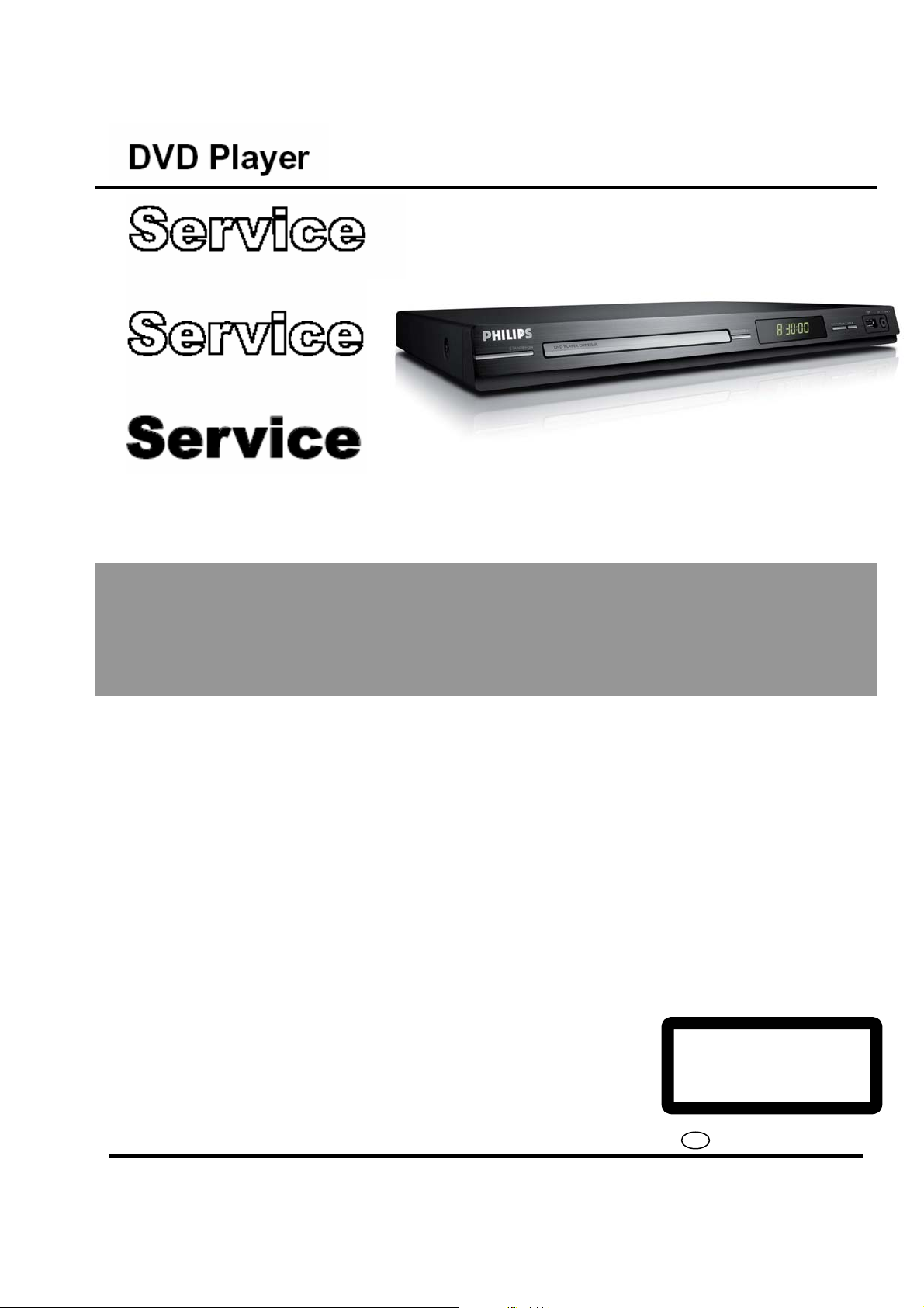
DVP3254K
DVP3254K/77
Service Manual
TABLE OF CONTENTS
Technical Specifications……………………………………..............1-2
. Safety Instruction, Warning & Notes….……………………....….....1-3
. Mechanical and Dismantling Instructions…………........................2-1
. Region Code, Software Version& Upgrades……………...............
. Trouble Shooting Chart………………………………………………
. Wiring Diagram………………………………………..………..….….5-1
. Electrical Diagrams and Print-layouts..….…………………....….…6-1
. Set Mechanical Exploded view & Part list.…………………..….….7-1
. Revision List…………………………………………………….…......8-1
©Copyright 2008 Philips Consumer Electronics B.V. Eindhoven, The Netherlands
All rights reserved. No part of this publication may be reproduced, stored in aretrieval system or
transmitted, in any form or by any means, electronic, mechanical, photocopying, or otherwise
without the prior permission of Philips.
Page
.3-1
.4-1
CLASS 1
LASER PRODUCT
Published by KC-0808 Service Audio Printed in The Netherlands Subject to modification
Version 1.0
GB
3139 785 33570
PHILIPS
Page 2

1-2
Specications
TV STANDARD
(PAL/50Hz) (NTSC/60Hz)
Number of lines 625 525
Playback Multistandard (PAL/NTSC)
VIDEO PERFORMANCE
Video DAC 12 bit, 108 MHz
Y Pb Pr 0.7 Vpp ~ 75 ohm
Video Output 1 Vpp ~ 75 ohm
VIDEO FORMAT
Digital MPEG 2 for DVD, SVCD
Compression MPEG 1 for VCD
DivX®
DVD 50 Hz 60 Hz
Horiz. resolution 720 pixels 720 pixels
Vertical resolution 576 lines 480 lines
VCD 50 Hz 60 Hz
Horiz. resolution 352 pixels 352 pixels
Vertical resolution 288 lines 240 lines
AUDIO PERFORMANCE
DA Converter 24 bit, 192 kHz
DVD fs 96 kHz 4 Hz - 44 kHz
fs 48 kHz 4 Hz - 22 kHz
SVCD fs 48 kHz 4 Hz - 22 kHz
fs 44.1kHz 4 Hz - 20 kHz
CD/VCD fs 44.1kHz 4 Hz - 20 kHz
Signal-Noise (1kHz) > 90 dB
Dynamic range(1kHz) > 80 dB
Crosstalk (1kHz) > 70 dB
Distortion/noise (1kHz) > 65 dB
MPEG MP3 MPEG Audio L3
CONNECTIONS
Y Pb Pr Output Cinch 3x
Video Output Cinch (yellow)
Audio Output(L+R) Cinch (white/red)
Digital Output 1 coaxial
IEC60958 for
CDDA / LPCM
IEC61937 for
MPEG 1/2,
Dolby Digital
AUDIO FORMAT
Digital MPEG/ AC-3/ compressed
PCM Digital
16, 20, 24 bits
fs, 44.1, 48, 96 kHz
MP3 (ISO 9660) 96, 112, 128,
256 kbps &
variable bit rate
fs, 32, 44.1, 48 kHz
Analog Sound Stereo
Dolby Surround compatible downmix from Dolby
Digital multi-channel sound
CABINET
Dimensions (w x h x d) 360 x 37x 209 mm360 x 37x 209 mm
Weight Approximately
2kg2kgkg
POWER CONSUMPTION
Power Supply Rating 110 V – 240 V;
50/60 Hz
Power consumption < 10 W
Power consumption in < 1 W
Standby mode
Specications are subject to change without prior
notice.
Page 3

1-3
Safety instruction, Warning & Notes
Safety instruction
1. General safety
Safety regulations require that during a repair:
. Connect the unit to the mains via an isolation transformer.
. Replace safety components indicated by the symbol ,
only by components identical to the original ones. Any
other component substitution (other than original type)
may increase risk of fire or electrical shock hazard.
Safety regulations require that after a repair, you must
return the unit in its original condition. Pay, in particular,
attention to the following points:
. Route the wires/cables correctly, and fix them with the
mounted cable clamps.
. Check the insulation of the mains lead for external
damage.
. Check the electrical DC resistance between the mains
plug and the secondary side:
1) Unplug the mains cord, and connect a wire between
the two pins of the mains plug.
2) Set the mains switch the “on” position (keep the
mains cord unplug).
3) Measure the resistance value between the mains
plug and the front panel, controls, and chassis
bottom.
4) Repair or correct unit when the resistance
measurement is less than 1M
5) Verify this, before you return the unit to the
customer/user (ref. UL-standard no. 1492).
6) Switch the unit “off”, and remove the wire between
the two pins of the mains plug.
¡
.
2.Laser safety
This unit employs a laser. Only qualified service personnel
may remove the cover, or attempt to service this device
(due to possible eye injury).
Laser device unit
Type : Semiconductor laser GaAlAs
Wavelength : 650nm (DVD)
: 780nm (VCD/CD)
Output power : 7mW (DVD)
: 10mW (DVD /CD)
Beam divergence: 60 degree
Note: Use of controls or adjustments or performance of
procedure other than those specified herein, may result in
hazardous radiation exposure. Avoid direct exposure to
beam.
Page 4

Warning
1-4
1.General
. All ICs and many other semiconductors are susceptible to
electrostatic discharges (ESD). Careless handing during
repair can reduce life drastically. Make sure that, during
repair, you are at the same potential as the mass of the
set by a wristband with resistance. Keep components and
tools at this same potential. Available ESD protection
equipment:
1) Complete kit ESD3 (small tablemat, wristband,
connection box, extension cable and earth cable)
4822 310 10671.
2) Wristband tester 4822 344 13999.
. Be careful during measurements in the live voltage
section. The primary side of the power supply , including
the heat sink, carries live mains voltage when you
connect the player to the mains (even when the player is
“off”!). It is possible to touch copper tracks and/or
components in this unshielded primary area, when you
service the player. Service personnel must take
precautions to prevent touching this area or components
in this area. A “lighting stroke” and a stripe-marked
printing on the printed wiring board, indicate the primary
side of the power supply.
. Never replace modules, or components, while the unit is
“on”.
2. Laser
. The use of optical instruments with this product, will
increase eye hazard.
. Only qualified service personnel may remove the cover
or attempt to service this device, due to possible eye
injury.
. Repair handing should take place as much as possible
with a disc loaded inside the player.
. Text below is placed inside the unit, on the laser cover
shield:
CAUTION: VISIBLE AND INVISIBLE LASER
RADIATION WHEN OPEN, AVOID EXPOSURE
TO BEAM.
Notes: Manufactured under licence from Dolby
Laboratories. The double-D symbol is trademarks of Dolby
Laboratories, Inc. All rights reserved.
Page 5

Notes
Lead-Free requirement for service
1-5
INDENTIFICATION:
Regardless of special logo (not always indicated)
One must treat all sets from 1.1.2005 onwards, according
next rules.
Important note
be treated in this way as long as you avoid mixing
solder-alloys (leaded/ lead-free). So best to always use
SAC305 and the higher temperatures belong to this.
Due to lead-free technology some rules have to be
respected by the workshop during a repair:
x Use only lead-free solder alloy Philips SAC305 with
order code 0622 149 00106. If lead-free solder-paste is
required, please contact the manufacturer of your
solder-equipment. In general use of solder-paste within
workshops should be avoided because paste is not easy
to store and to handle.
x Use only adequate solder tools applicable for lead-free
solder alloy. The solder tool must be able
o To reach at least a solder-temperature of 400°C,
o To stabilize the adjusted temperature at the
o To exchange solder-tips for different applications.
x Adjust your solder tool so that a temperature around
360°C
joint. Heating-time of the solder-joint should not exceed
~ 4 sec. Avoid temperatures above 400°C otherwise
wear-out of tips will rise drastically and flux-fluid will be
destroyed. To avoid wear-out of tips switch off un-used
equipment, or reduce heat.
x Mix of lead-free solder alloy / parts with leaded solder
alloy / parts is possible but PHILIPS recommends
strongly to avoid mixed
solder alloy types (leaded and lead-free). If one cannot
avoid, clean carefully the
solder-joint from old solder alloy and re-solder with new
solder alloy (SAC305).
: In fact also products a little older can also
solder-tip
– 380°C is reached and stabilized at the solder
x Use only original spare-parts listed in the
Service-Manuals. Not listed standard-material
(commodities) has to be purchased at external
companies.
x Special information for BGA-ICs:
- always use the 12nc-recognizable soldering
temperature profile of the specific BGA (for
de-soldering always use highest lead-free
temperature profile, in case of doubt)
- lead free BGA-ICs will be delivered in so-called
‘dry-packaging’ (sealed pack including a silica gel
pack) to protect the IC against moisture. After
opening, dependent of MSL-level seen on
indicator-label in the bag, the BGA-IC possibly
still has to be baked dry. This will be
communicated via AYS-website.
Do not re-use BGAs at all.
x For sets produced before 1.1.2005, containing
leaded soldering-tin and components, all needed
spare-parts will be available till the end of the
service-period. For repair of such sets nothing
changes.
x On our website:
www.atyourservice.ce.Philips.com
You find more information to:
BGA-de-/soldering (+ baking instructions)
Heating-profiles of BGAs and other ICs used in
Philips-sets
You will find this and more technical information
within the “magazine”, chapter “workshop news”.
For additional questions please contact your local
repair-helpdesk.
Page 6
2-1
Mechanical and Dismantling Instructions
Dismantling Instruction
The following guidelines show how to dismantle the player.
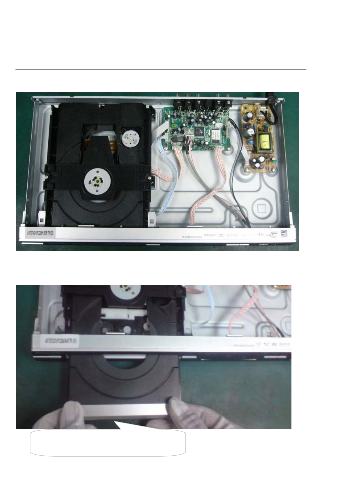
Step1: Remove 5 screws around the Top Cover, and then remove the Top Cover (Figure 1).
Figure 1
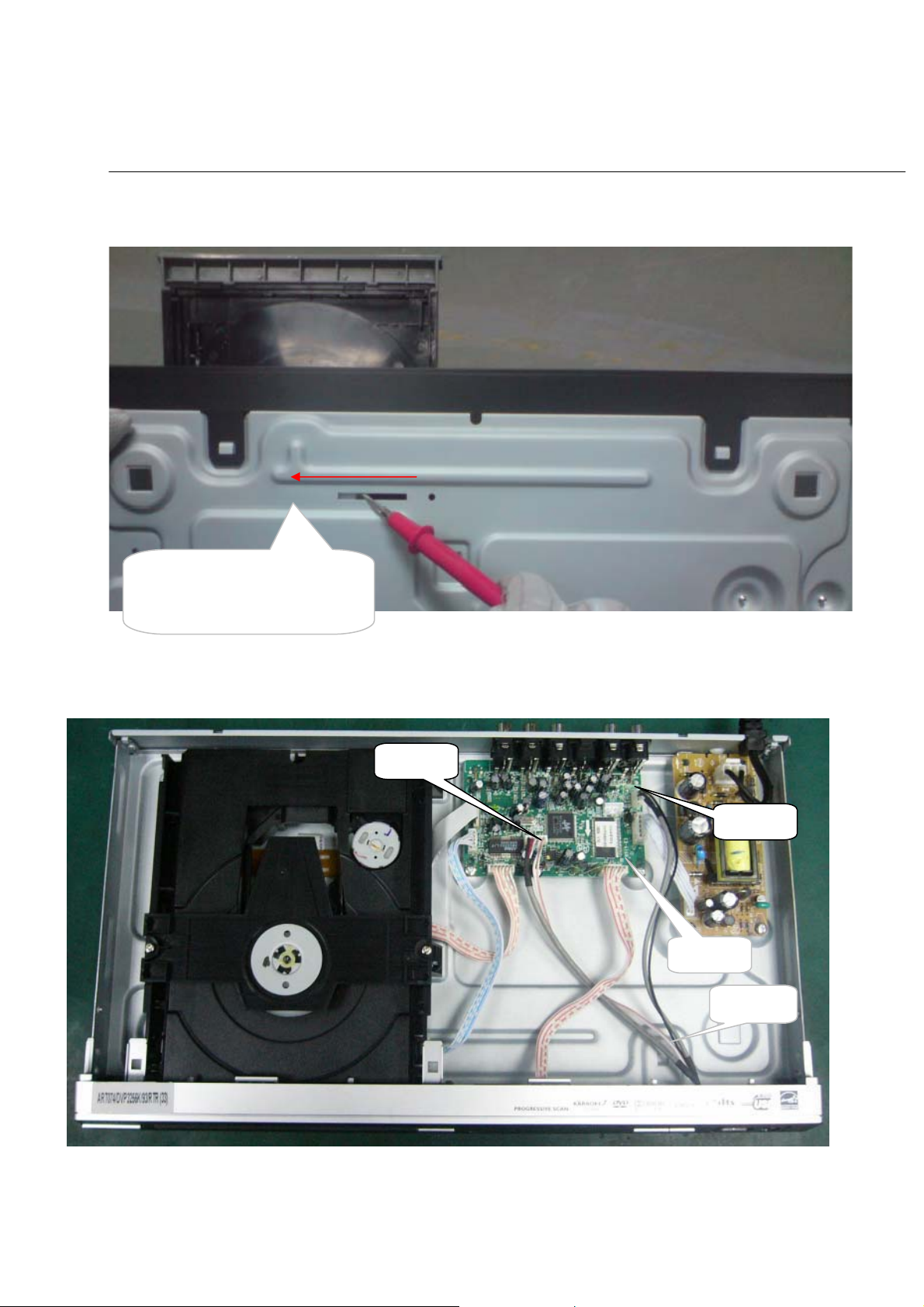
Step2: If it is necessary to dismantle Loader or Front Panel, the Front door should be removed first. (Figure 2)
Note: Make sure to operate gently otherwise the guider would be damaged.
Please kindly note that dismantle the front door
assembly carefully to avoid damage tray and the front door.
Figure 2
Page 7
2-2
Mechanical and Dismantling Instructions
Dismantling Instruction
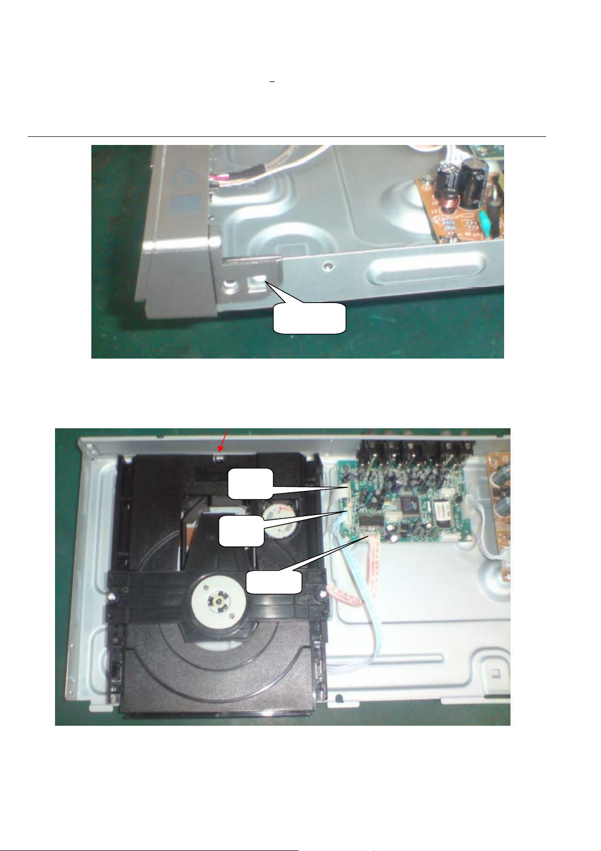
Step3: If the tray can’t open in normal way, you can make it through the instruction as below (Figure 3).
Note: Make sure to operate gently otherwise the guider would be damaged.
Push the guider until the tray out.
Make sure to operate gently to
avoid damage happening.
Figure 3
Step4: Dismantling Front Panel, disconnect the connectors (XP5, XP6. XP7), then release the snaps on the both sides of Front
Panel and bottom cabinet , then gently pull the Panel out from the set. (Figure 4 & 5)
XP7
XP6
XP5
Snap 1
Figure 4
Page 8
2嗽3
Mechanical and Dismantling Instructions
Dismantling Instruction
Snap 2
Figure 5
Step5: Dismantling Loader, disconnect the 3 connectors (XP2, XP3, XP4) aiming in the below figure, and remove 1 screw that
connects the loader and the bottom cabinet. (Figure 6)
XP2
XP3
XP4
Figure 6
Page 9
2-4
Mechanical and Dismantling Instructions
Dismantling Instruction
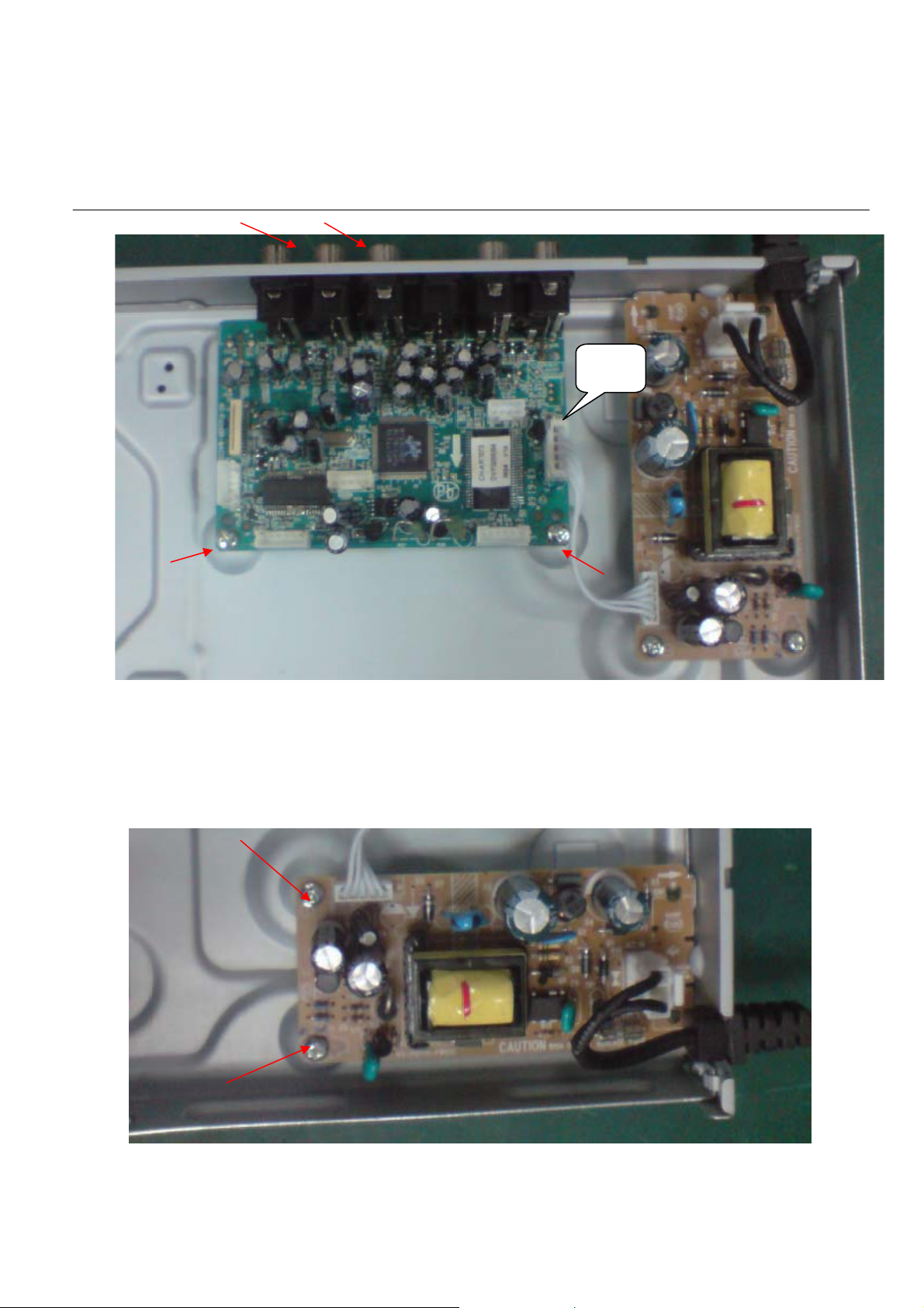
Step6: Dismantling Main Board, first disconnect the connector (XP1), and then remove 4 screws. (Figure 7)
XP1
Figure 7
Step7: Remove the 2 screws on Power Board to dismantle the Power Board. (Figure 8)
Figure 8
Page 10

3-1
Software upgrade
Preparation to upgrade software
1) Start the CD Burning software and create a new CD
project (Data Disc) with the following setting:
Label: DVP3XXX (No need the label name)
File Name: DVPXXXX_XX.BIN
Power on the set and open the tray, then press <5><5>
to check the File Name.
Note: It is required capital letter for the File System
name.
2) Burn the data onto a blank CDR
A. Procedure for software upgrade:
1) Power on the set and insert the prepared Upgrade
CDR.
2) The set will starts reading disc & response with the
following display TV screen:
Upgrade File DETECTED
Upgrade?
Press Play TO START.
3) Press <OK> button to confirm, then screen will display :
Files coping…
UPGRADING…
4) The upgraded tray will automatically open when files
coping complete, then take out the disc.
5) About 1 minute later, the trace will automatically close
when upgrading complete.
B. Read out the software versions to confirm upgrading
1) Power on the set and press <Setup> button on the
remote control.
2) Press <1><3><7><9> button.
The software version and other information are display
on the TV screen as follows:
Version XX.XX.XX.XX (Main version)
SUB-VER XX.XX.XX.XX (software version of
application software)
8032 XX.XX.XX.XX
Servo XX.XX.XX.XX (software version of
Servo)
RISC XX.XX.XX.XX
DSP XX.XX.XX.XX
Region Code X
Caution: The set must not be power off during
upgrading, Otherwise the Main board will be
damaged entirely.
Page 11

3
嗽
2
How to select the right language
If the language is not right, it can be corrected by
the following operation:
1. Power on the set and open the tray.
Press “6” “6” “6” “6” and “Audio” button on the
remote control.
After that on the screen it shows:
PLS INPUT MODEL CODE:
2. Then input the related MODEL CODE “0”.
After that on the screen it shows:
hhhhh
DVP
(It means the language has been corrected and
the player will be power off automatically.)
REGION h OK
Page 12
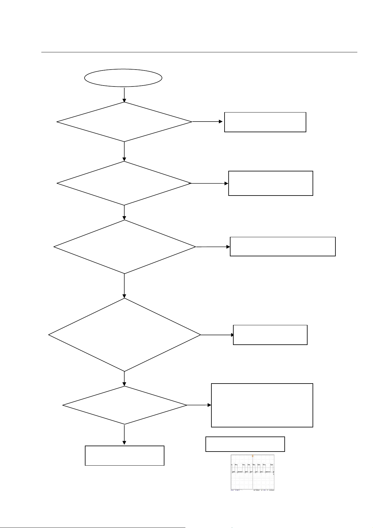
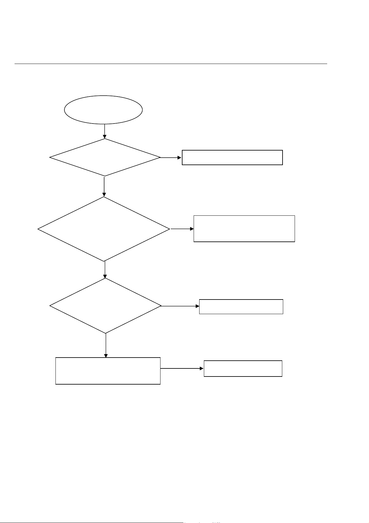
Spindle motor does not move
Motor no move
Go
4-1
Trouble shooting chart
Check the FFC connection
between 24P and the loader.
Yes
Check whether “M5V”
(+5V) voltage is normal.
Yes
Check whether laser voltage
(1.9V for CD & 2.4V for DVD)
on L9 and L10
Yes
No
No
No
Correct connection
Check the M5V power supply
Check/Replace Q5,Q6,Q7,Q8.
1.Whether voltage on pin 23 of U1
varies between 0 and 3.3V (3.3V for
CD and 0V for DVD),
2.Whether peripheral components
are eroded or badly soldered.
Yes
Check opu focus
Yes
Check/Replace the loader
No
1. Check U1 25pin FOCUS_PWM
No
signals
2.If there are F+, F-, T+ and T-
signals output from U2.
FOCUS_PWN waveform
Check/ Replace U1.
Page 13
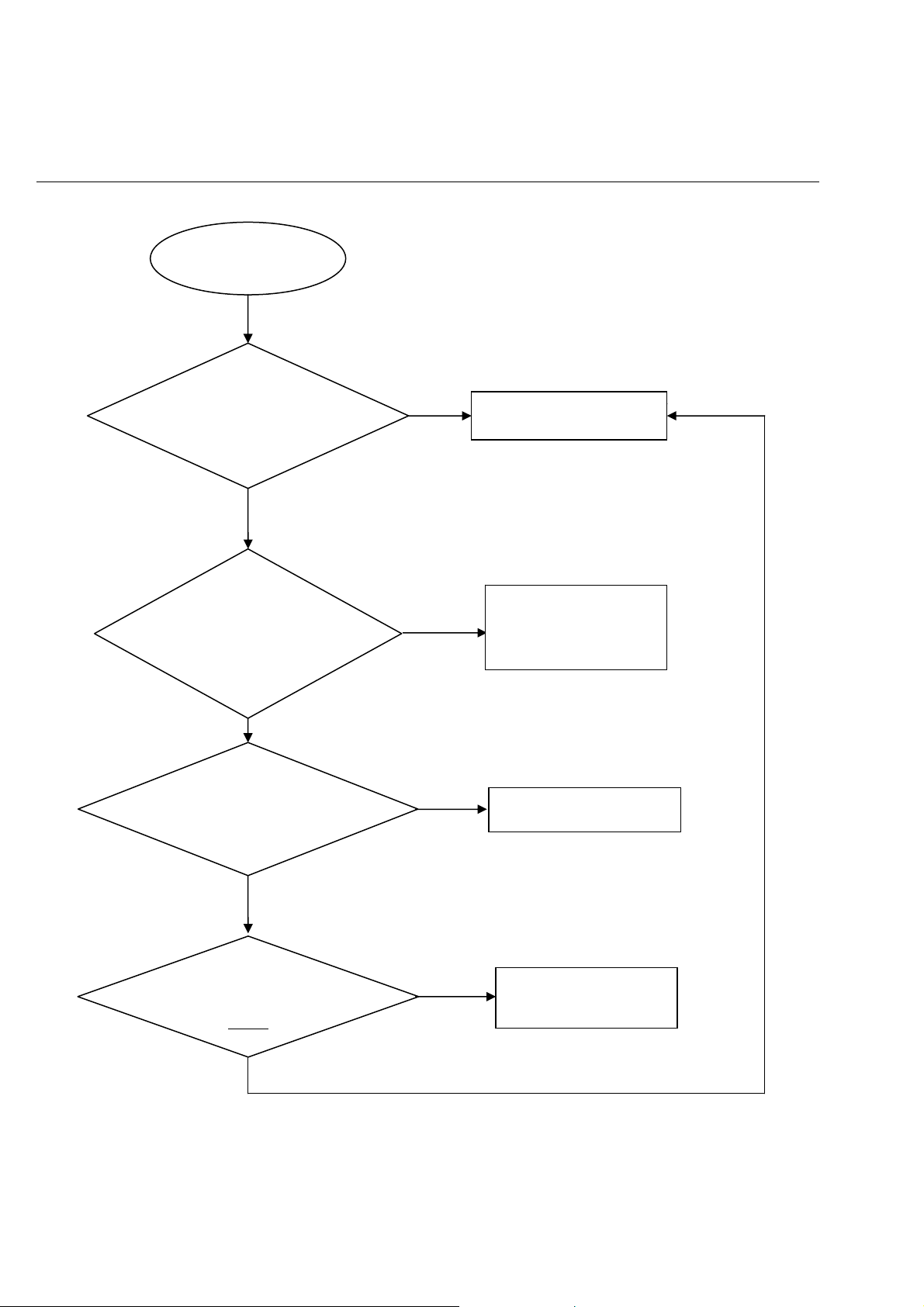
The power can not be on or off
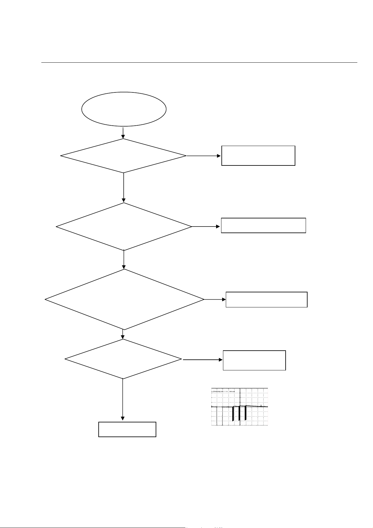
The power can’t be
on or off
Go
4-2
Trouble shooting chart
Check the power supply
on the power board is
normal.
Yes
Check if the XS301 on the
front board to XP5 on the
decoder board is in good
contact.
Yes
Whether the connection
to K301 is broken.
Ye s
No
No
No
Repair the power board
Check/Correct
connection
Correct the connection
Yes
Whether there is 0V and
3.3V voltage difference on
Pin 106 PCON
Yes
of U1.
No
Replace U1.
Page 14
4-3
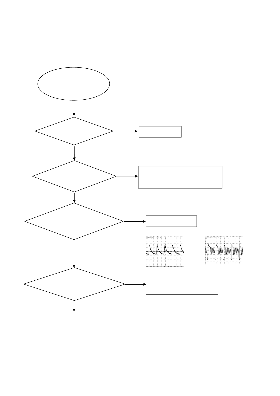
All output voltages on the power board is 0V or deviated.
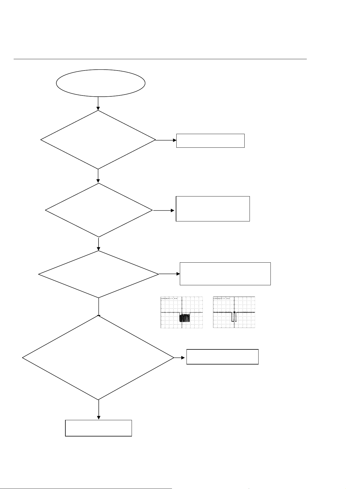
All output voltages on
the power board is 0V or
deviated
Yes
Trouble shooting chart
Check whether
F1 is blown
No
Check whether there is
300V on C1 or C2.
Yes
Check whether 100KHz
oscillating signal on
Pin6 of U1
Yes
Yes
No
No
Replace F1
Replace C1&C2 if D1, D2, D3, D4 are
normal.
Check/ replace U1.
U1(PIN 3 - RC waveform)
U1(PIN 8 - Drain waveform)
Check if +5V and +12V are
short.
Yes
Check whether the components in the
short-circuit voltage are defected or eroded.
No
Check whether U1 are eroded.
Page 15
Disc cannot be read.
Disc cannot be read.
Yes
4-4
Trouble shooting chart
Check the FFC connection
between 24P and the loader.
Yes
Check whether there is laser
voltage (1.9V for CD and 2.4V for
DVD) on L9 and L10.
Yes
Check U1, U2, and
peripheral components are
eroded or badly soldered.
No
No
No
Check the loaded circuit
1.Check voltage on pin 23 of U1 varies
between 0 and 3.3V:
Æ3.3V for CD
Æ0V for DVD
2.Check whether peripheral components
are eroded or defect
Re-solder or replace the defective parts
Yes
Check if there is RFO signal on
pin17 of XP2. (The normal RFO
signal is a clear reticulated wave)
Yes
Check the connection
between U1
Yes
Replace U1 or loader.
No
No
Check U1 and peripheral components
Correct connection
Page 16
4-5
p
Only DVD disc or only disc except DVD can be played
Only DVD disc, or only disc
except DVD can be Played.
Go
Trouble shooting chart
Check the FFC
connection between
24pin and the loader.
Yes
Check laser voltage (2.4V) output
on L10, if pin18 of U1 is at low
level.
Yes
Check whether there
is voltage variance on
in 25 of U1.
No
No
No
Check the loaded circuit
Check the solder status on U1 and
peripheral components
check if bad solder exist on U1 and
peripheral components
Yes
Check whether pins of U1 and
peripheral components are
badly soldered, defected
Yes
Check Q5, Q7
whether in good
Yes
Change U1 or the loader.
No
Replace the bad spare parts
No
Correct connection
Page 17
No display on LED, and buttons do not work
No display on LED, and
buttons do not work
Yes
4-6
Trouble shooting chart
Check whether there is
correct contact between
XS301 and XP5
Yes
Check VCC(+5v) voltage
on the power and front
board
Yes
Check there are STB, SDA
and SCK signals on XS301
on the front board.
No
Correct connection
No
No
XP5 (PIN 1 CLK) XP5 (PIN3 DOUT)
Fix power supply board top
a power supply for should
electric circuit
Check the U1’s pin 87,41,40 arrive
the XP5 connect condition
Yes
1.Check whether bad solder exists on
U301 and pins of LED,
2.Check whether the circuit connected to
K302, K303, K304 and K301 is broken,
3.Check whether R300, R301 and R302
are open-circuit.
Yes
Replace U301 or LED
No
Correct connection
Page 18
Distorted audio and loud noise
Distorted audio and
loud noise
Yes
Check the power supply voltages
+12V to the operation amplifying
Q3 is normal.
Yes
No
4-7
Trouble shooting chart
Check Q3
Check whether the muting transistor
R84,R94,R100,R107,R116,R124 are
normal
Yes
Check whether the muting
transistor Q11,Q12,
Q13,Q15,Q17,Q19are normal
Yes
Checking the U6 leads the
feet has no to break to
open
Yes
Check the voltage on
pin3 or pin5 of U6 is OK.
(Should be 2.5~3.1V)
No
No
No
Replace R84, R94,R100,R107,R116,R124
Replace Q11~Q19
&RUUHFWFRQQHFWLRQ
No
Replace R86,R87
Yes
Check whether the U1 or
U6 powersupply normal
Yes
Replace U1 or U15
No
Check U6
Page 19
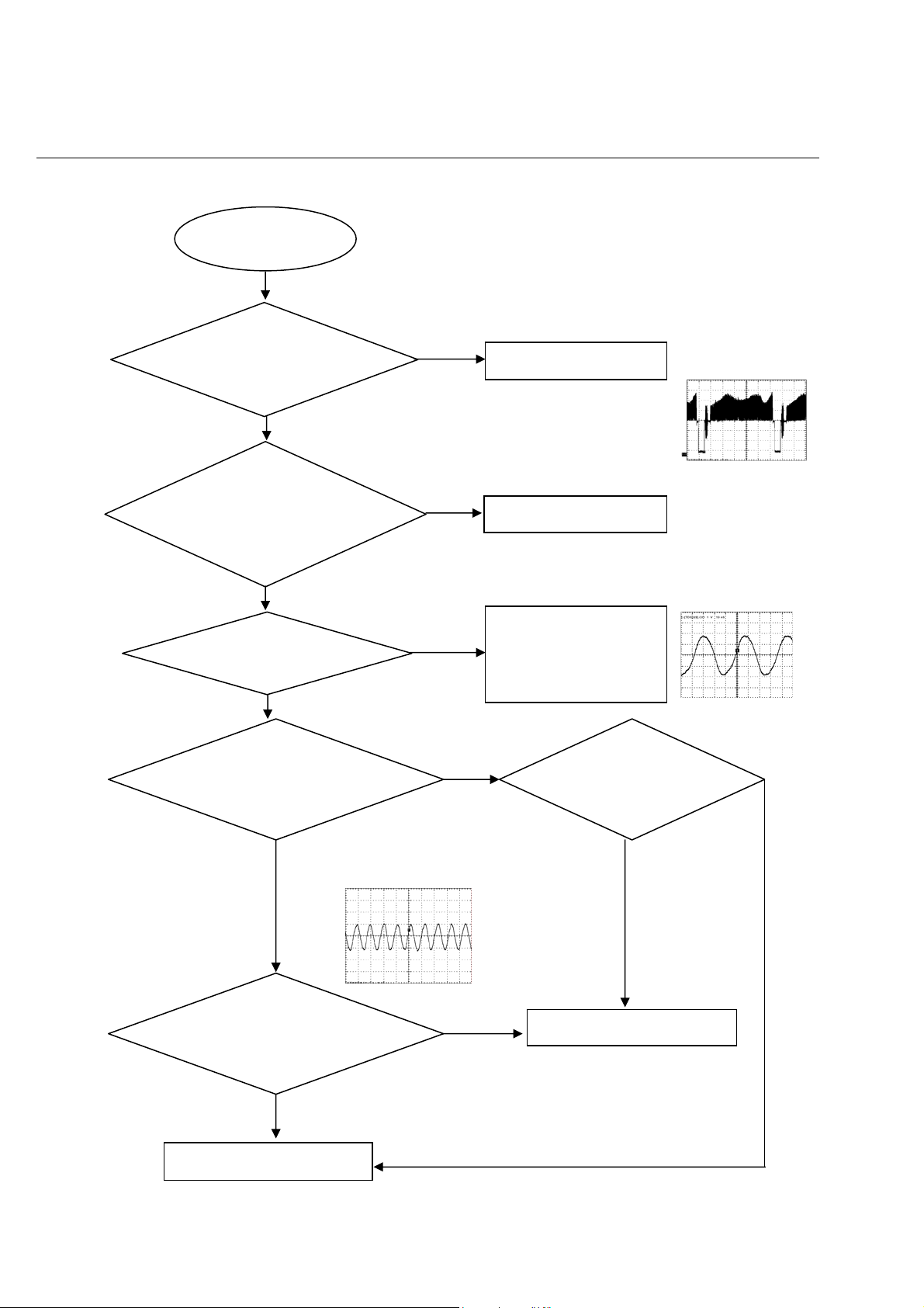
Abnormal color of video picture
p
p
Abnormal color of
video
icture
Yes
4-8
Trouble shooting chart
Check whether the
27MHz out
Yes
Check whether the 3.3V
and 1.8V power supply
voltages on the decoder
board are normal.
Check whether the
video filter network
circuit is normal.
ut signal
Yes
No
Check Y2, R20,R27,C22 and C23
No
Check other of power supply electric
circuit
No
Correct the connection
Yes
Check if the video signals on Pin
99,102,103,104, of U1 are normal
No
change U1
Page 20
Remote reception is insensitive or fails.
p
Remote reception is
insensitive or fails.
Go
4-9
Trouble shooting chart
Check if the remote
control works
roperly.
Yes
Check if the power supply
voltage to the remote censor
is normal
Yes
Use an oscilloscope to check if there is
output waveform from the first pin IR of the
remote censor after pressing button on the
remote control.
Yes
No
No
Check battery
Check R315ǃC315
No
REM301(PIN1 - RC waveform)
Check if there is IR
signal on pin 44 of U1
Yes
Change U1
IR waveform
No
Correct connection
Page 21
No video picture, no sound.
y
No video picture,
no sound.
4-10
Trouble shooting chart
Check whether all the voltages
from the power board to the
decoder board are normal.
Yes
Check if the reset circuit consisting
ofCE7, D2 is normal (at a low level
for tens of milliseconds, then
at 3.3V).
constantl
Yes
Check whether there is
27MHz signal output.
Yes
Check if there is 128MHz
signal output on R67.
No
No
No
Check the loaded circuit
Change CE7, D2.
Crystal oscillator Y2 and
peripheral components
are defected or eroded.
No
CVBS(R21 point) waveform
27Mhz waveform
Check whether
short-circuit or bad
solder on U4,U5
SDRAM(R67 DCLK) waveform
No
Yes
Check if short-circuit and
bad solder exist on Pin
99
No
Check U1.
Yes
Yes
Reconnect the component in
Page 22
5-1
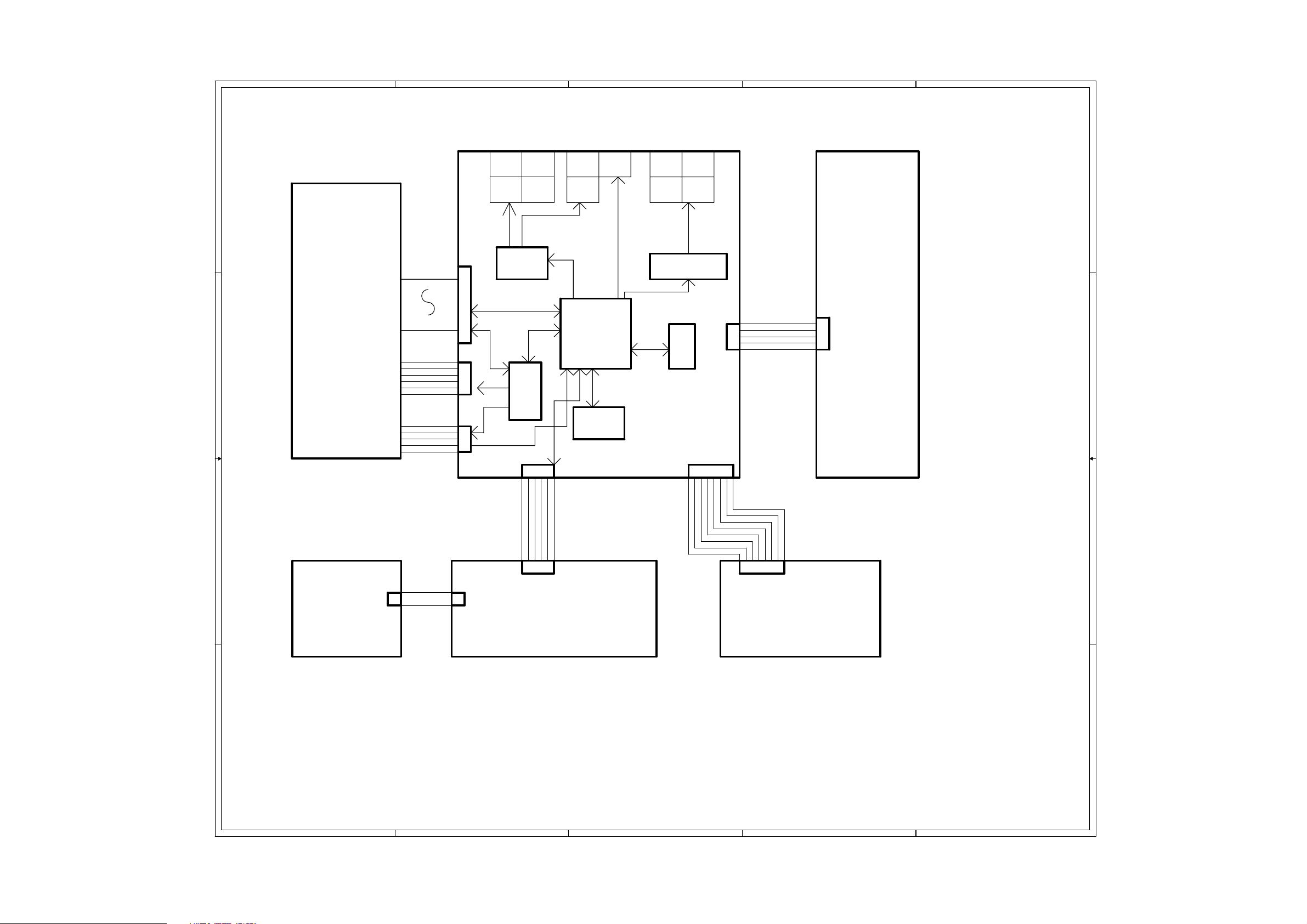
5-1
A
DVP3254K/77WIRING DIAGRAM
WIRING
B
C
D
E
DIAGRAM
SW SR
4 4
CN SL
1
24
SP-
3 3
DVD LOADER
SP+
LIMIT
GND
SLSL+
1
6
LOAD+
LOAD-
(TCL)TDM-2+SONY KHM313AAM
TROUT
GND
TRIN
1
5
AUDIO
AMP&LPF
XP2
24PIN*0.5
XP4
6PIN*2.0
XP3
5PIN*2.0
6PIN*2.0
AM5888
MOTER DRIVER
XP5
1
R
COAX
L
P2
MT1389L
8M/16M
FLASH
MAIN BOARD
618
Pr
Pb
VIDEO LPF&DRIVE
Y
CVBS
16M /64M
SDRAM
XP6
8PIN*2.0
P1
1
XP1
5PIN*2.5
5
5V
5V
GND
12V
GND
1
XS201
5PIN*2.5
5
POWER
SUPPLY
CLK
CS
DATA
GND5VIR
MIC
GND
12V
5V
GND
USB_DN
USB_DP
2 2
61
XS301
SWITCH
BOARD
XP303
2PIN*2.0
2
1
GND
POWER_K
1
2
XS302
2PIN*2.0
6PIN*2.0
GND
18
XS601
8PIN*2.0
KARAOKE AND USB
LED DISPLAY+ET6202/KEY
Remark: For DVP3254K/77, 8PIN*2.0 XP6 is divided into 5PIN*2.0 XP7 and 3PIN XP6
5PIN*2.5 XP1 is the same as 5PIN CABLE TJC3-5Y/SCN-5P L=70MM
8PIN*2.0 XP6 is the same as 8PIN CABLE WITCH SHIELD
1 1
6PIN*2.0 XP5 is the same as HS 6P PH-6Y/JC20-6Y 150MM
5PIN*2.0 XP3 is the same as HS 5P 2468#26 150MM PH-5Y*2
6PIN*2.0 XP4 is the same as HS 6P PH-6Y/PH-6Y
24PIN*0.5 XP2 is the same as 24PIN HS
A
B
C
D
E
Page 23
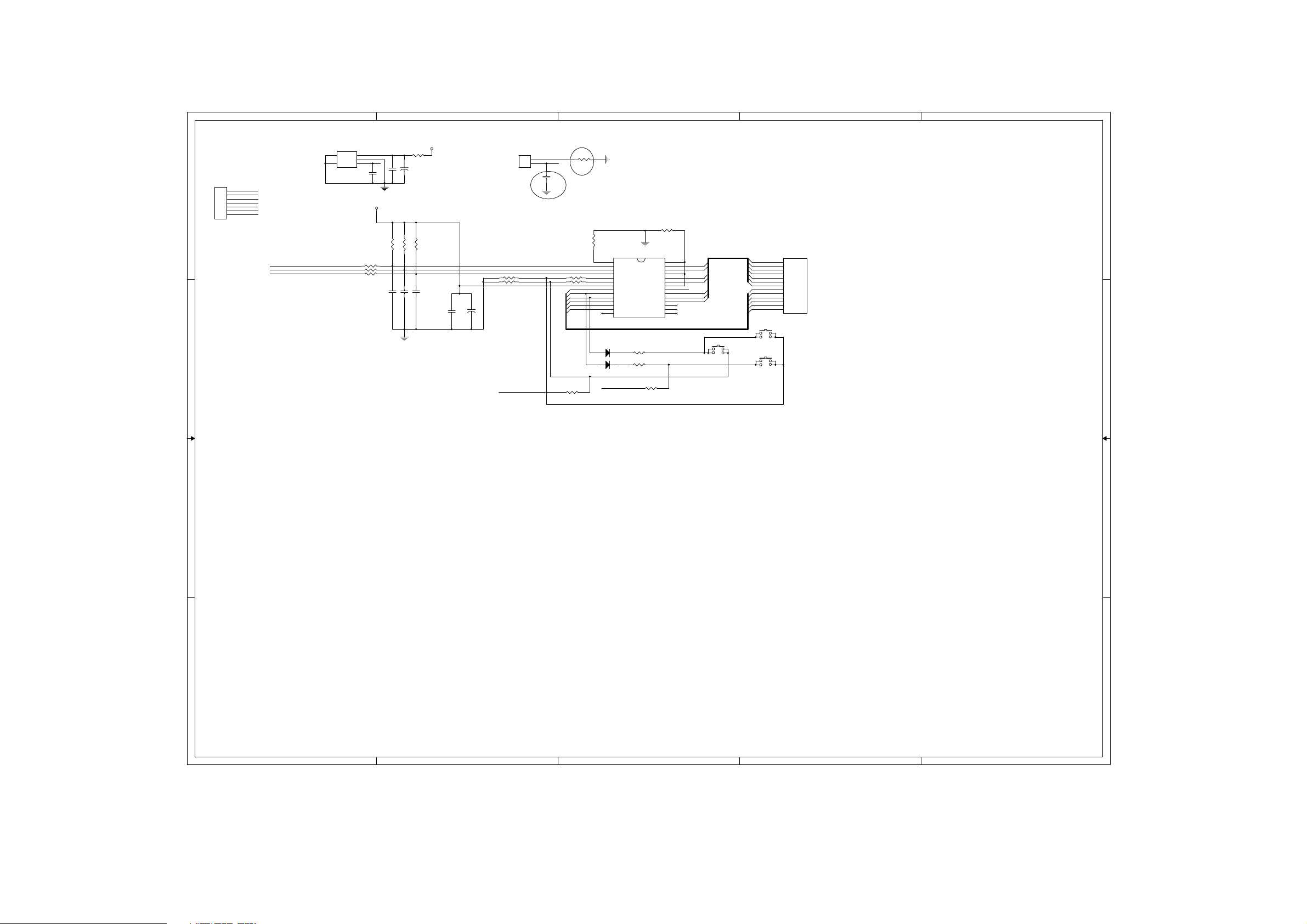
6-1
6-1
A
Front Board Electric Diagram
REM301
3
5
VCC45
2
GND
IR
1
4
IR
)5200$,1%2$5'
XS301
IR
1
5V
2
GND
3
DATA
CON7(2.0)
4
CS
5
CLK
6
POWER_K
7
CLK
CS
1 1
REM
R300 100
R301 100
R302 100
C306
0.1u
C315
47p
5V
R303
4K7
C300
100P
5V
R315
100 ohm
+
CE301
47uF
R304
R305
4K7
4K7
C301
C302
100P
100P
2 2
3 3
B
XS302
POWER_K1
1
POWER_K
2
CON2(2.0)
5VL
R307 10K
R308 10K
CE300
C303
+
0.1u
47uF
POWER_K1
R316
0/NC
C316
0.1u/NC
R306
51K
1
OSC
2
DI/O
3
CLK
4
R309 1K
R310 1K
SEG1
SEG2 SEG2
SEG3
SEG4
SEG5
SEG6
KEY1
KEY2
R318 0/NC
5
6
7
8
9
10
11
12
13
14
SEG[1:6]
D3011N4148
D3021N4148
POWER_K
STB
KEY1
KEY2
VDD
SEG1/KS1
SEG2/KS2
SEG3/KS3
SEG4/KS4
SEG5/KS5
SEG6/KS6
SEG7/KS7
ET6202
U301
SEG14/GRID5
SEG13/GRID6
SEG12/GRID7
R312 1K
R311 1K
R317 0/NC
C
R319 0
GRID1
GRID2
GRID3
GRID4
SEG10/KS10
SEG9/KS9
SEG8/KS8
KS1
KS2
D
C300
GRID1
GRID2
GRID3
GRID4
GRID5
GRID6
GRID7
SEG1
SEG3
SEG4
SEG5
SEG6
LED1
1
GRID1
2
GRID2
3
GRID3
4
GRID4
5
GRID5
6
GRID6
7
GRID7
8
SEG1
9
SEG2
10
SEG3
11
SEG4
12
SEG5
13
SEG6
JDD350501AG
K303
play/pause
K302
stop
28
GND
GND
GND
VDD
GRID1DATA
27
GRID2
26
25
GRID3
24
GRID4
23
22
5VL
21
GRID7
20
GRID6
19
GRID5
18
17
16
15
open/close
GRID[1:7]
K304
C301
C302
C303
C306
C315
C316
CE300
CE301
D301
D302
K302
K303
K304
LED1
R300
R301
R302
R303
R304
R305
R306
R307
R308
R309
R310
R311
R312
R315
R316
R317
R318
R319
REM301
U301
XS301
XS302
E
B2
B2
B2
B2
B1
A1
B1
B2
B1
C2
C2
D2
D2
C2
D1
A1
A1
A1
B1
B1
B1
C1
B1
B1
B1
B1
C2
C2
B1
C1
C2
B2
C1
A1
C1
A1
B1
4 4
A
B
C
D
E
Page 24
6-2
6-2
A
B
C
D
E
Switch Board Electric Diagram
1 1
K301
1
1
2
2
CN301
SWITCH BOARD
2 2
stop
3 3
4 4
A
B
C
D
E
Page 25
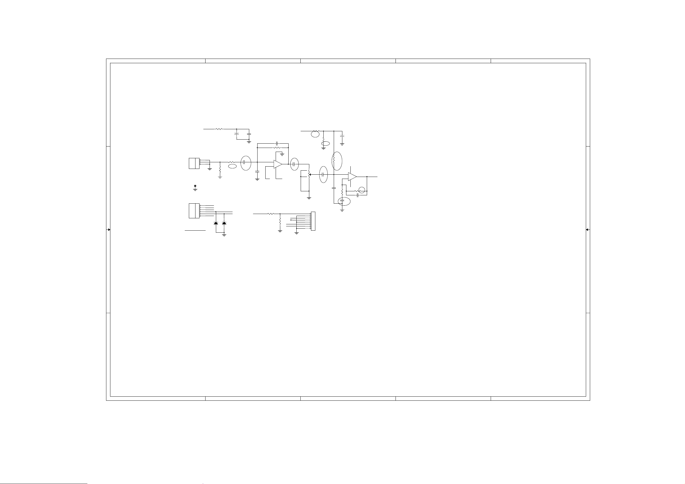
6-3
6-3
A
B
C
D
E
OK+USB Board Electric Diagram
1 1
ĭ3.5mm
P601
KARAOKE INPUT
1
2
3
KARAOKE
47-EAR024-XX0
G1
R210
12V
150
R200
10K
12VA
C201
CE201
0.1u
22uF
C210
R201
1uF
1.8K
C203
1000p
C205 47p
R205 68K
REF
U200A
C211
-
2
1
+
3
8 4
NJM4558
12VA
1uF
2 2
P600
USB
USB
GND AGND
1
2
3
4
5
47-USB003-XX2
6
GND
GND
VCC
USB_DN
USB_DP MIC_OUT
GND
D30
5V1
R208
D31
5V1
1K
12V
VCC
R209
USB_DN
680
USB_DP
3 3
MIC
12VA
5
4
RP200
10K
8PIN/2.0mm
R202
22K
2
1 3
1
2
3
4
5
6
7
8
XP601
REF
CE200
R203
22K
22uF
C201
C203
C204
C205
R211
100K
C208
1uF
84
NJM4558
5
+
6
-
C209
1uF
U200B
R207 20K
C206 47p
C204
100p
R206
3.9K
MIC_OUT
7
C206
C208
C209
C210
C211
CE200
CE201
D30
D31
G1
P600
P601
R200
R201
R202
R203
R205
R206
R207
R208
R209
R210
R211
RP200
U200A
U200B
XP601
B1
B2
C2
B1
C2
C2
C2
B2
B2
C1
B1
B2
B2
A2
A2
A2
B2
B2
C1
C1
B1
C2
C2
B2
B2
B1
C2
B2
B2
C2
C2
4 4
A
B
C
D
E
Page 26
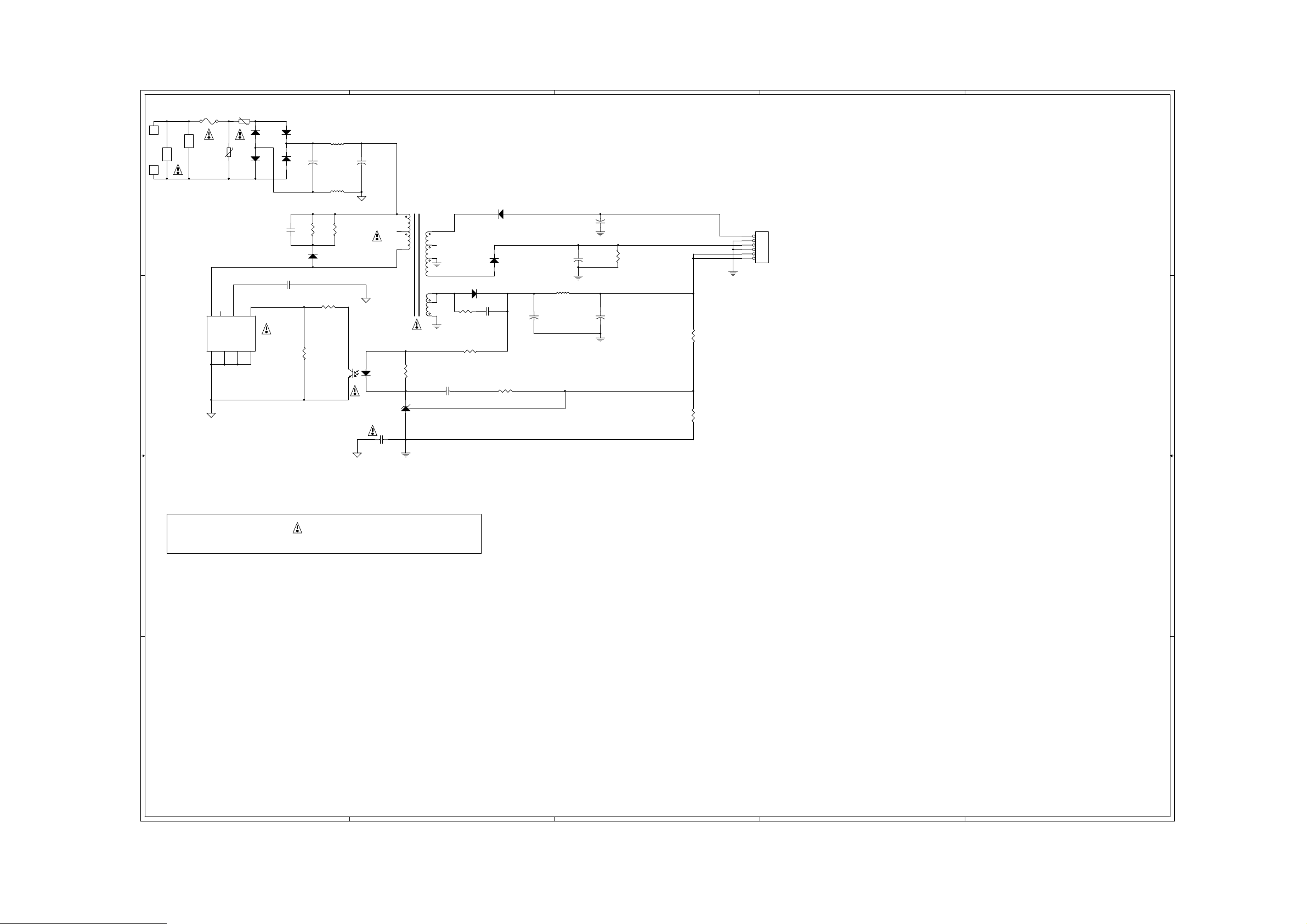
6-4
6-4
5
F1
++
1 2
CN1
AC INPUT
T2AL/250ac
++
CON1
AC INPUT
1 2
P3
1
AC INPUT
1
P2
D D
C C
3
Drain
U1
TNY176/177
S
5
NC
S
647
NTC 10&20
RV1
10K471
2
BP/M
S
TR1
D1
1N4007
1N4007
S EN/UV
8 1
D2
1N4007
D3
D4
1N4007
152/1KV
C9
104/50V
C5
R13
1/6W100k
L1
680uH
C1
+
10uF/400V(250V/450V)
L6
⺕⦴
R2
R3
1/4W120K
1/4W120K
D8
IN4007
R11
1/6W22
U2
PC123X92
+
43
C2
15uF/400V(250V/450V)
5
4
3
12
U3
TL431
CY1
102/400Vac
3
2
T1 EEL19
R8
1/6W1k
1
* CAUTION :
THE PARTS MARKED WITH ARE IMPORTANT PARTS ON THE SAFETY.
PLEASE USE THE PARTS HAVING THE DESIGNATED PARTS NUMBER WITHOUT FAIL.
B B
4
Power Board Electric Diagram
D5
D10 SR360/SR340
C14
NU
R10
1/6W100
FR102
D7
FR102
R9
1/6W10k
+
C7
1000uF/16V
L2
6.8uH
C6
+
47uF/25V
6
7
9
8
12
11
10
0.1uF/63V
R1
NU
C11
C3
+
+
470uF/16V
10uF/50V
C8
R4
1/6W10k
3
CON2
6
-22V
5
GND
4
+12V
3
GND
2
+5V
1
+5V
6X2.5 HEADER
R5
1/6W12K 1%
R7
1/6W11.3k 1%
2
C1
C11
C14
C2
C3
C5
C6
C7
C8
C9
CN1
CON1
CON2
CY1
D1
D10
D2
D3
D4
D5
D7
D8
F1
L1
L2
L6
P2
P3
R1
R10
R11
R13
R2
R3
R4
R5
R7
R8
R9
RV1
T1
TR1
U1
U2
U3
A1
B2
B2
B1
C1
A1
C1
B2
C2
A2
A1
A1
C1
B2
A1
B2
A1
A1
A1
B1
B1
A1
A1
A1
B2
A1
A1
A1
B2
B2
A2
A2
A1
A1
C1
C2
C2
B2
B2
A1
B1
A1
A2
A2
B2
1
A A
5
4
3
2
1
Page 27
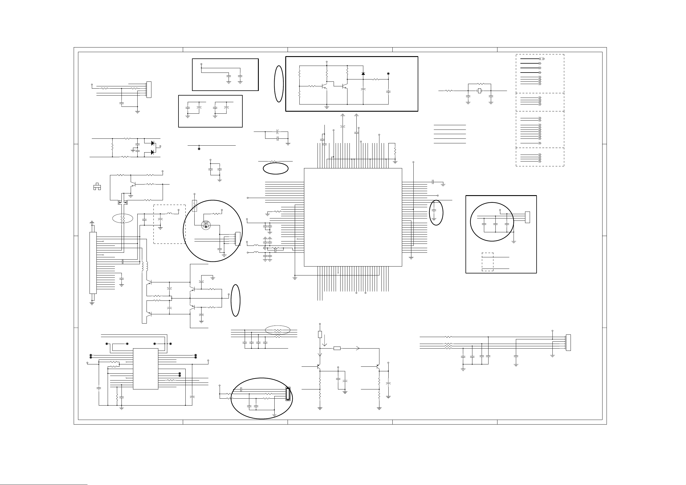
6-5
6-5
A
Main Board Electric Diagram: MT1389L/K LQFP 128
XP4
DV33
SP+
R23 10k
1 1
LIMIT
SLSL+
C20
0.1uF
SP-A
R128 1k
6PIN/2.0mm
1
2
3
4
5
6
C87
0.1uF
V18
V18 RFV18-1
V18 RFV18-2
V20
+
CE8
47uF/6.3v
C88
0.1uF
RF Reference
1
C27
2
0.1uF
R34 10k
R35 10k
R36 100k
L9
OP-
D3
3
BAT54C
OPO
C32
0.1uF
Very Important to
reduce Noise
L10
10uH
Q7
9012
R45 4.7
R46 4.7
Q8
9012
TP10
VOFC+
VOFC-
VOSL-
VOSL+
VOTR+
VOTR-
VCC
G1G2
REV
FWD
REGO1
VINSL+
REGO2
TRB1
VINFC
DV33
M5V
+
14
13
12
11
10
9
8
2930
7
6
5
4
3
2
1
IOA
L6
FB
CE10
100uF/16v
LOAD+
LOAD-
TROPEN
TRCLOSE
R56 10k
FOSO
+
CE11
47uF/6.3v
CE12
+
47uF/6.3v
TP11
MDI1
TP4
V18
C85
0.1uF
Chip Decap.
M5V
F1
TP16
TP17
[FUSE(500MA)]
R4
4.7K
1
2 3
AO3402
Q20
USB_DM
USB_DP
C92
0.1uF
LDO2
CE33
+
100uF/10V
Q23
R49 10k
9012
Q24
R32 10k
9012
CE34
+
100uF/10V
LDO1
SP-
TP13
SP+
TP15
M5V
REG01
DMSO
CE15
+
220uF/16v
REG02
TR_B1
DV33
M5V
S
LD-DVD
AVCC1
MDI1
LD-CD
E
AVCC1
V20
F
B
A
RFO
IOA
D
C
TT+
F+
F-
F+
TP8
R54 10k
R55 10k
C95
0.1uF
R24 10k
R25
1
R28 10k
R33 100k
2
Q5
2SK3018
R38
100
C94 0.1uF
TT+
FMSO
TR_B2
TRSO
V1P4
STBY
R61
10k
C24
0.1uF
Q4
2N3904
13
13
2
Q6
2SK3018
R39
100
10uH
C37
NC
TP9
U2
15
VOTK+
16
VOTK-
17
VOLD+
18
VOLD-
19
VCC2
20
NC
21
VCTL
22
GND
23
VINLD
24
NC
25
TRB2
26
VINTK
27
BIAS
28
MUTE
AM5888
C96
0.1uF
SP-
SP-A
D
3
G
21
2 2
2SK3018
SC-70
SONY 313
RFGND
XP2
SMD0.5 TOP
25
26
1
2
3
4
5
6
7
8
9
10
11
12
13
14
TOP
1
3 3
TP12
TP14
15
16
17
18
19
20
21
22
23
24
27
28
RFGND
SL+
SL-
M5V
4 4
B
C84
C83
0.1uF
0.1uF
SERVO RF DeCAP.
V1P4
+
CE9
47uF/6.3v
MDI2
C86
0.1uF
RFVDD3
+12V
DV33
XP7
5PIN/2.0mm
1
2
3
DV33
4
5
V18
DV33
FOSO
TRSO
FMSO
DMSO
C38
330pF
C49 0.1uF
R62 10k
TROUT
R63 10k
TRIN
C18
0.1UF
ADVCM
FB3 0R
FB4 0R
10uF/10v
C39
330pF
C33
4.7uF
C91
0.1uF
C36
C40
0.1uF
R9 1K
R11 1K
C19
0.1UF
CE31
+
10uF/16v
C89 0.1uF
1389_OP+OPO
R31 0/NC
C
B
A
D
F
E
RFV18-2
RFVDD3
XI
XO
R37 15k
LDO1
LDO2
AVDD33
C90
0.1uF
C34
10uF/10v
R40 5.1k
C35 NC
C93
0.1uF
R41 27k
R42 27k
R43 15k
R44 10k
C41
0.015uF
V1P4
LOADLOAD+
V20
V1P4
MDI1
MDI2
DMO
FMO
STBY
IOA
TRO
FOO
USB_DP
USB_DM
USB_V33
USB_V18
FOO
TRO
FMOFDMO
XP3
1
2
3
4
5
PITCH 2.0mm*5
R15
15K
R17
3.3K
R16
4.7K
U1
1
RFA
2
RFB
3
RFC
4
RFD
5
RFE
6
RFF
7
AVDD18
8
AVDD33
9
XTALI
10
XTALO
11
AGND
12
V20
14
REXT
15
MDI1
16
MDI2
17
LDO1
18
LDO2
19
AVDD33
20
DMO
21
FMO
22
TRAY_OPEN
23
TRAY_CLOSE
24
TRO
25
FOO
26
FG / GPIO2
27
USB_DP
28
USB_DM
29
USB_V33
30
USB_GND
31
PAD_VRT
32
USB_V18
2.2 OHM 2W
TR_B1
SS8550D
C29
1uF
2N3904
OP-
1389_OP+
128
127
RFH / OPINN
C
DV33
R18
3.3K
Q21
RFO
C30
220pF
126
125
RFG / OPINP
RFIN / OPOUT
Q22
2N3904
CE32
+
ADACVDD
10uF/16v
AVCM
AL
AR
ALS
ALF
ADACVDD
RFV18-1
124
123
118
117
116
122
121
120
119
RFIP
AGND18
AVDD18
AVCM
AL / GPIO1
ALF / GPIO
ALS / GPIO
ADACVDD2
ADACVDD1
ARS
115
AR / GPIO0
ARS / GPIO
R19
22K
ARF
112
113
114
ARF / GPIO
ADACVSS2
ADACVSS1
RESET Circuit
1N4148
D2
CE7
+
22uF/16v
CEL5-5
APLLVDD3
C28 1500pF
AADVDD
GPIO19
AADVDD
GPIO21
GPIO20
APLLVDD3
111
110
109
108
107
106
AADVDD
APLLCAP
APLLVDD
ADVCM / GPIO20
AKIN1 / GPIO21 / Audio_Mute
AKIN2 / GPIO19 / Audio_Mute
V_R
105
104
AADVSS
MT1389L/K
LQFP 128
Desktop
V1.0
GPIO3 / INT#
GPIO4
SF_CS_
SF_DO
SF_DI
SF_CK
UP1_6 / SCL
UP1_7 / SDA
ICE
PRST#IRRD0
RD1
RD2
RD3
RD4
RD5
RD6
RD7
DVDD33
DQM0
RD15
DQ4
DQ2
DQ3
Imax=250mA
standby:27MA
CE13
220uF/16v
DVDD18
DQ5
DQ6
DQ7
V18DV33
TR_B2
SS8550D
REG02REG01
DQ14
DQ15
DQM0
b
Q10
GPIO6
33343637383940414243444546474849515253505556575458596162636064
35
GPIO3TROUT
GPIO6TROPEN
SF_CK
UP1_7
UP1_6
R126
M5V
GPIO4LIMIT
SF_DI
SF_DO
SF_CS
Imax=600mA
R127
DQ1
DQ0
URST#
IR#
standby:87MA
5.6 OHM 1W
Imax=350mA
DV33
Q9
R57
C48
+
0.1uF
20k/1%
R59
RFGND
12k/1%
GND
URST#
TP3
R26
URST#
1K
C21
1uF
C21 must closer to PIN43 of 1389L/K.
DACVDD3
CVBS_OUT
DACVDD3
1009998
CVBS
DACVSSC
DACVDDB
SPDIF / GPIO12
RD11
RD10
RD9
DQ10
DQ11
DQ9
V18
GND
FS
97
FS
VREF
DACVDDC
GPIO13
GPIO11
GPIO10
DVDD18
GPIO9
GPIO8
GPIO7 / CKE
RA3
RA2
DVDD33V14
RA1
RA0
RA10
BA1
DVSS18
BA0
RAS#
CAS#
RWE#
RA4
RA5
RA6
RA7
RA8
RA9
DVDD33
RA11
RCLK
DQM1
RD8
MT1389L/K/SMD
MTK1389L/K-128
DQ8
CE14
+
220uF/16v
R29
560
96
95
94
93
92
91
90
89
88
87
86
85
8413
83
82
81
80
79
78
77
76
75
74
73
72
71
70
69
68
67
66
65
R
RD14
V_B
103
DQ13
B
RD13
V_G
102
DQ12
DACVDD3
101
G
DACVDDA
RD12
DVSS33
ec
R58
5.1k/1%
R60
10k/1%
GND
DV33
C31 0.1uF
VREF
DACVDD3
GPIO13
GPIO12
GPIO11
GPIO10
GPIO9
GPIO8 TRCLOSE
GPIO7
MA3
MA2
MA1
MA0
MA10
BA1
BA0
RAS#
CAS#
WE#
MA4
MA5
MA6
MA7
MA8
MA9
MA11
DCLK
DQM1
IR#
UP1_7
GPIO7
UP1_6
D
R27 33
XO
ADVCMGPIO20
GPIO12 ASPDIF
GPIO11 AUDIO_MUTE
GPIO13 TRIN
V18
C17
NC(100p)
R50 33
R51 100/0402
R52 100/0402
R53 100/0402
AKIN1GPIO21
C44
NC(47p)
C22
27pF
R20 100k
RS-232
NC(100p)
C45
NC(47p)
Y2
27MHz
C16
NC(100p)
Default
GPIO9 RXD
C43
47p
C42
NC(47p)
E
DQ[0..15]
MA[0..11]
DQM[0..1]
BA[0..1]
DCLK
RAS#
CAS#
WE#
C23
27pF
XI
DRAM I/F
SF_CK
SF_CS
SF_DI
SF_DO
S-FLASH
GPIO19
AKIN1
ASPDIF
AR
AL
ARF
ALF
ARS
ALS
AUDIO_MUTE
AUDIO I/F
CVBS_OUT
V_R
V_B
V_G
VIDEO I/F
DV33
C2
C10
NC(100p)
TXDGPIO10
RxD
TxD
3V3
GND
4pin/2.0mm
XP8
1
2
3
4
TO FRONT PANEL
C46
NC(100p)
MA[0..11] 4
DQM[0..1] 4
BA[0..1] 4
DCLK 4
RAS# 4
CAS# 4
WE# 4
SF_CK 4
SF_CS 4
SF_DI 4
SF_DO 4
PCON 2
AKIN1 5
ASPDIF 5
AR 5
AL 5
ARF 5
ALF 5
ARS 5
ALS 5
AUDIO_MUTE 5
CVBS_OUT 4
V_R 4
V_B 4
V_G 4
IRIR
VSDA
VSTB
VSCK
DQ[0..15] 4
5V
6PIN/2.0mm
XP5
6
5
4
3
2
1
A
B
C
D
E
Page 28
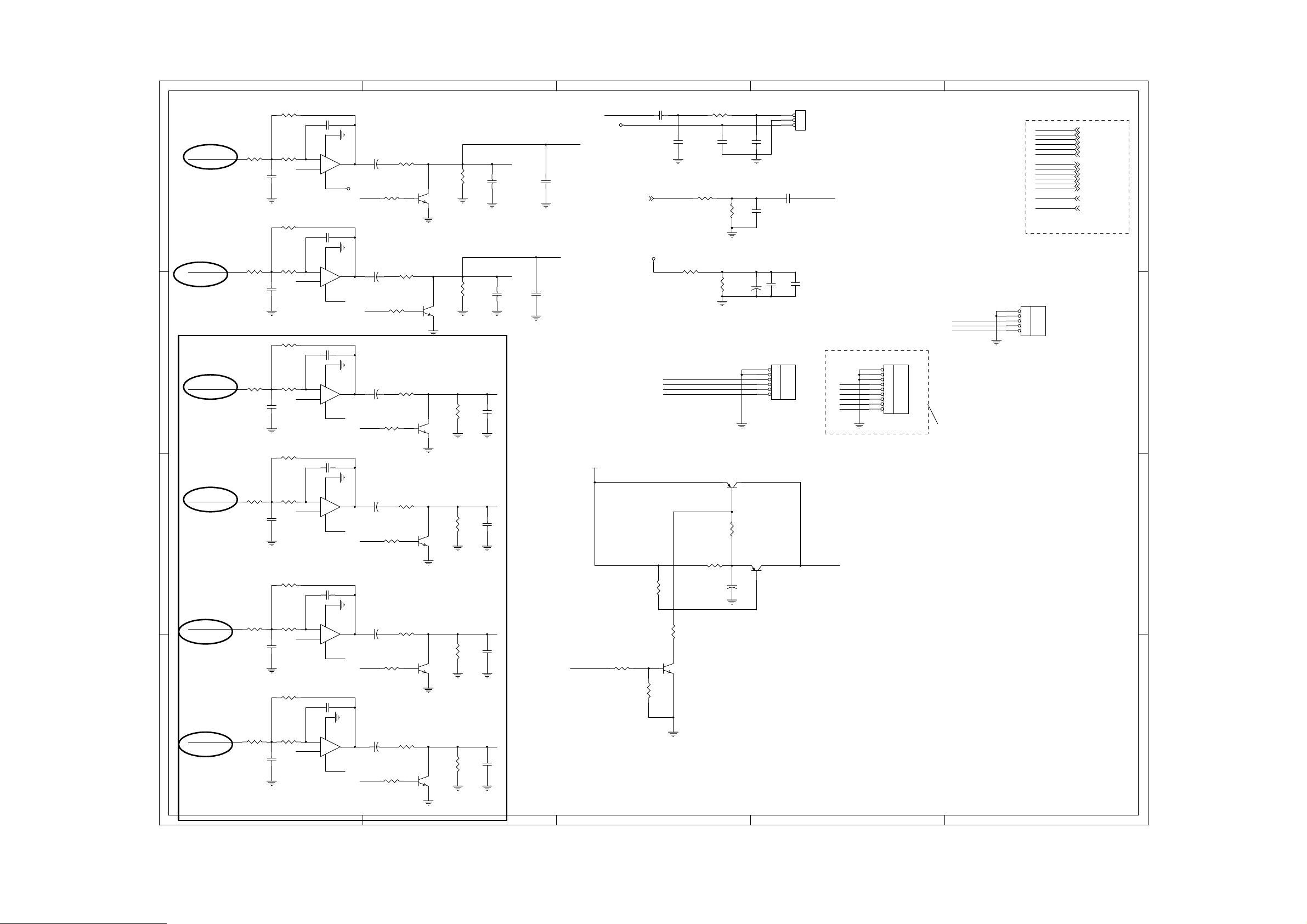
6-6
6-6
A
Main board Electric diagram: Audio I/F
R78
refa
refa
C60 100pF
U6A
-
2
+
3
NJM4558 OPA
8 4
+12VA
C66 100pF
U6B
-
6
+
5
NJM4558 OPA
8 4
+12VA
C71 100pF
CE18
R82
+
1
+12VA
A_MUTE
7
A_MUTE
10uF/16v
CE21
+
10uF/16v
470
R84
470
R92
470
R94
470
31k
R81
AL
R80
10k
1 1
AR
R90
10k
5.1k
C64
1000pF
R85
31k
R91
5.1k
C69
1000pF
R95
31k
2 2
R97
ARS
ALS
R96
10k
R102
10k
5.1k
C72
1000pF
R101
31k
R103
5.1k
C75
1000pF
refa
refa
3 3
R109
31k
U7B
-
6
+
5
NJM4558 OPA
8 4
+12VA
C74 100pF
U7A
-
2
+
3
NJM4558 OPA
8 4
+12VA
C77 100pF
CE23
R98
+
7
A_MUTE
1
A_MUTE
10uF/16v
CE25
+
10uF/16v
470
R100
470
R104
470
R107
470
Q11
2N3904
Q12
2N3904
Q13
2N3904
Q15
2N3904
B
RSCH
R99
100k
LSCH
R105
100k
R83
100k
R93
100k
LCH
C65
1000pF
RCH
C73
1000pF
C76
1000pF
C70
1000pF
FR
C103
1000pF
FL
C102
1000pF
M5V
+12VA
(
ᓔᴎ䴭䷇
C61 0.1uF
ASPDIF3
R110
3.3K
+12VA
C
)
C62
3300p
R88 100
R86 30k
LSCH
RSCH
CENT
SUB
R79 100
C101
0.1uF
refa
R87
10k
Q14
R108
10k
CE26
220U/16V
R89
100
CE19
100U/16V
9012
R106
4.7K
+
MICAKIN1
C63
100p
C68
330pF
+
RCA/AUDIO OUT
Q16
9012
3PIN/2.0mm
C67
0.1uF
C47
0.1U
1
2
3
4
5
6
XP6
1
2
3
C12
0.1uF
P3
47-RCA151-XX
RCA
D
COAXIALASPDIF
E
AR
AL
ARS
ALS
ARF
ALF
RCH
LCH
RSCH
LSCH
SUB
CENT
AKIN1
AUDIO_MUTE
AR 3
AL 3
ARS 3
ALS 3
ARF 3
ALF 3
RCH
LCH
RSCH
LSCH
SUB
CENT
AKIN1 3
AUDIO_MUTE 3
AUDIO I/F
P2
47-RCA149-XX1
1
RCA
2
3
4
5
A_MUTE
LSCH
RSCH
CENT
SUB
FL
FR
RCA/AUDIO OUT
1
2
3
4
5
6
7
8
9
P4
47-RCA217-XX1
RCA
COAXIAL
LCH
RCH
this component used only for
DVP3266K/93
RCA/AUDIO OUT
ALF
4 4
ARF
R111
10k
R120
10k
R112
5.1k
C78
1000pF
R119
31k
R121
5.1k
C81
1000pF
refa
refa
U8A
-
2
+
3
NJM4558 OPA
8 4
+12VA
C80 100pF
U8B
-
6
+
5
NJM4558 OPA
8 4
+12VA
CE28
1
A_MUTE
7
A_MUTE
10uF/16v
CE30
+
10uF/16v
470
R116
470
R122
470
R124
470
R114
+
Q17
2N3904
Q19
2N3904
CENT
R115
100k
SUB
R123
100k
C79
1000pF
C82
1000pF
AUDIO_MUTE
R117
4.7K
R118
22K
R113
4.7K
Q18
2N3904
Only for MT1389L,not for MT1389K.
A
B
C
D
E
Page 29
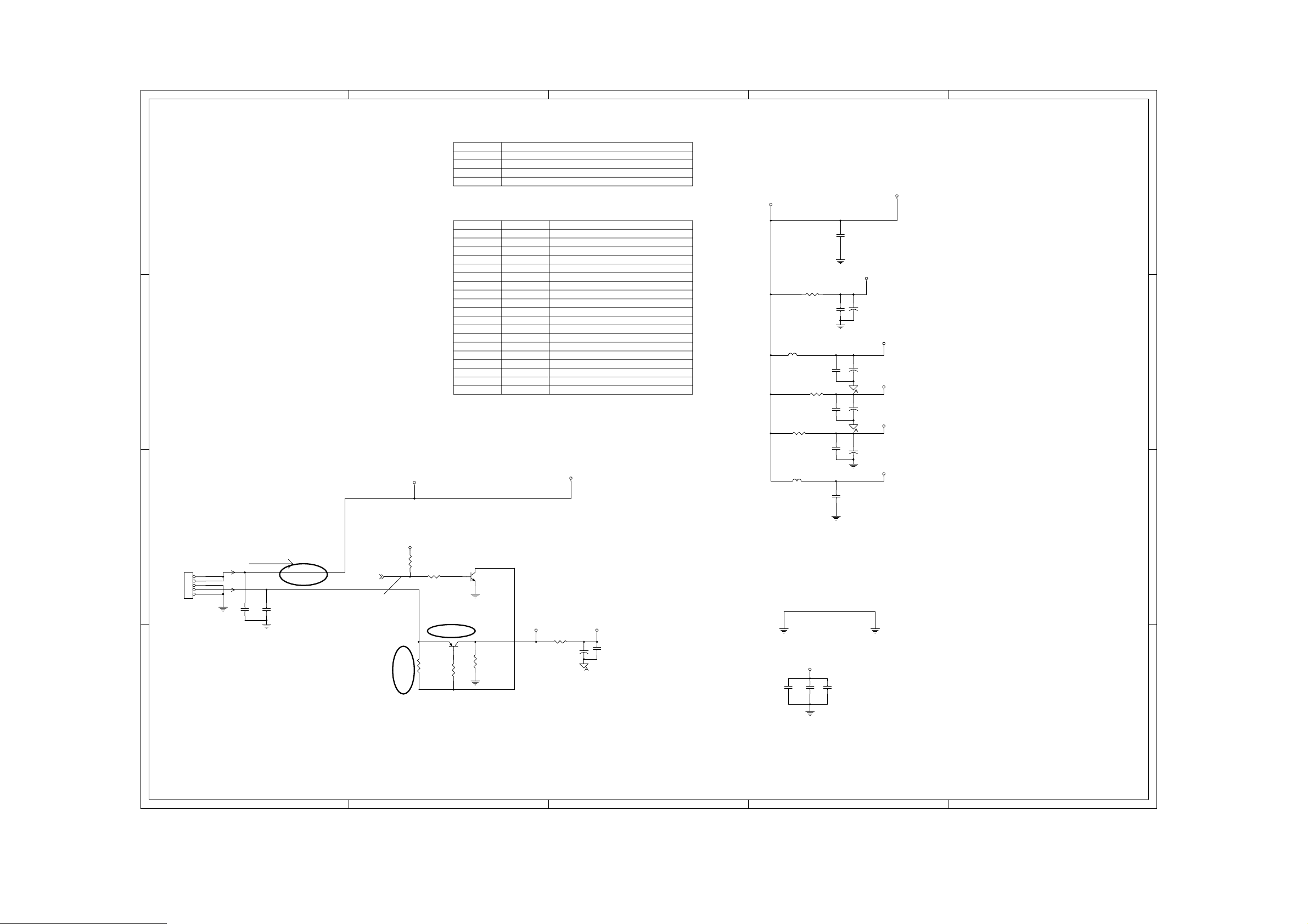
6-7
6-7
A
COMMON1389L/K_KHM313_AM5888_V2
Desktop Model
MT1389L/K (LQFP128) DVD TEST Board w/ Sony KHM Series PUHs
1 1
B
C
MT1389L/K Features Support List
(MIC/USB Only for MT1389L)
Item
1
2
3
4
Features
5.1CH(only 2CH for 89K) + USB + VFD + AMUTE
Main board electric diagram: POWER
DV33
D
RFVDD3
E
MT1389L/K General GPIO List
Name
GPIO3
GPIO4
GPIO6
GPIO7
GPO_A
GPO_B
GPIO2
GPIO8
GPIO9
GPIO10
GPIO11
GPIO12
GPIO19
GPIO20
2 2
M5V
M5V
GPIO21
GPIOK0
GPIOK1
GPIOK2
PIN
33
34
35
87
22 STBY
23
26
88
89
91
92
93
94
106
107
108
27
28
31
Features
TROUT
LIMIT
TROPEN
VSDA
IOA
OPO
TRCLOSE
AUDIO_MUTE
ASPDIF
TRINGPIO13
PCON
ADVCM
AKIN1
Only for 89K
Only for 89K
Only for 89K
5V
Imax 130mA
FB1
500
FB2
500
R3
4.7/0603
R1
4.7/0603
4.7/0603
C1
0.1uF
RFGND
AADVDD
RFGND
CE1
+
100U/16V
CE2
+
47uF/16v
CE3
+
470uF/6.3v
CE4
+
47uF/16v
AUDIO ADC
DACVDD3
ADACVDD
APLLVDD3
SD33
VIDEO DAC
AUDIO DAC
AADVDD
C3
0.1U
C4
0.1uF
R2
C5
0.1U
C6
0.1uF
C7
0.1uF
3 3
TO POWER BOARD
XP1
5pin/2.5mm
1
2
GND
3
+P12V
4
GND
5
+12V: +12V(+-10%)
+5V: +5V(+-2.5%)
Imax 800mA
C8
0.1uF
PCON3
C9
0.1uF
PCON:
L: STBY.
H: Working.
DV33
R8
4.7K
R7
1K
Q3
8550D
R13
22K
Q2
BT3904
GND AGND VGND MGNDRFGND
+12V
R10 100/0805
CE6
R12
4.7K
R14
4.7K
100uF/16v
+12VA
C11
+
0.1uF
VGND
C13
0.1uF
DV33
C14
0.1uF
GND
C15
0.1uF
4 4
A
B
C
D
E
Page 30
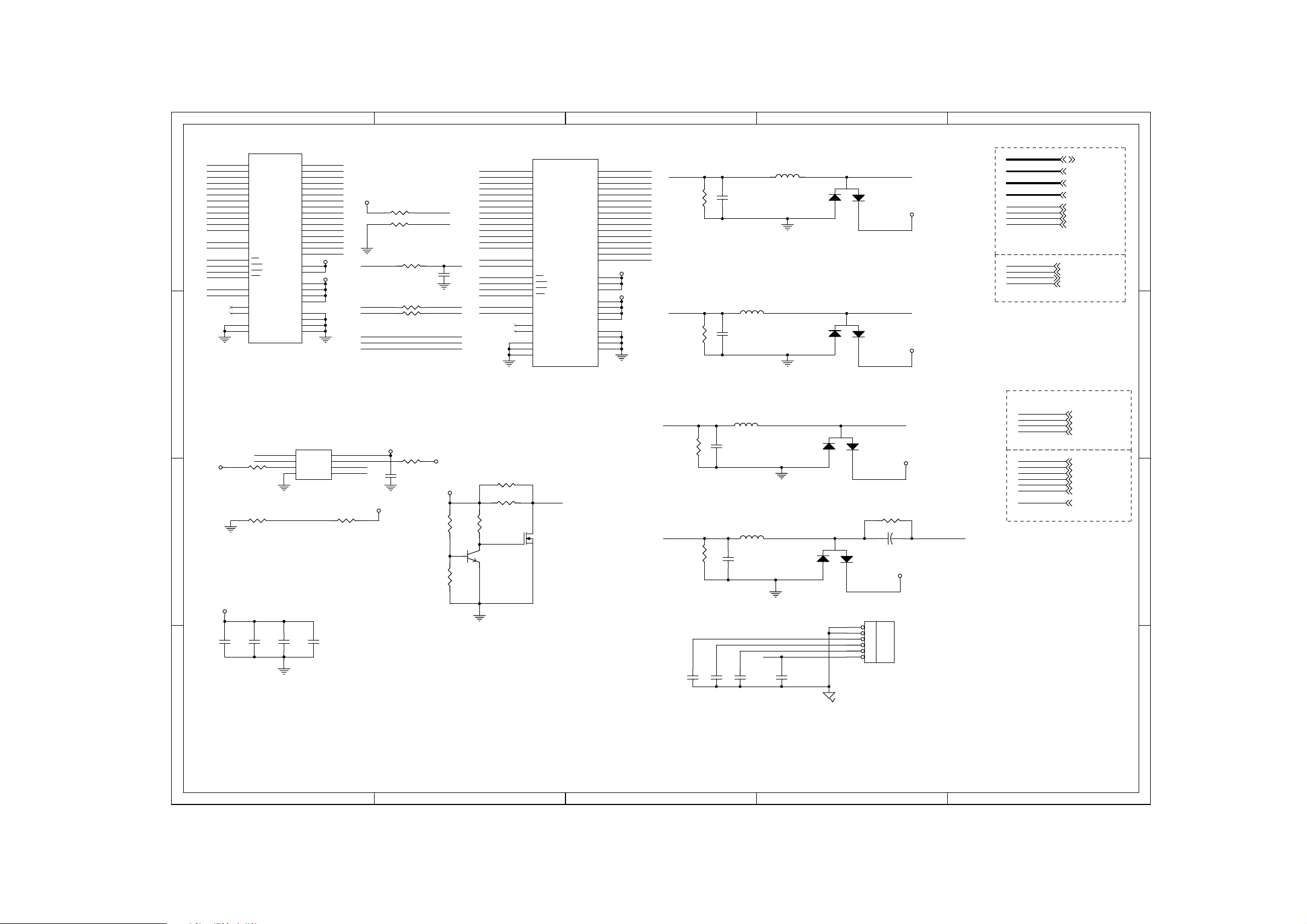
6-8
6-8
A
U3
MA0
21
MA1
MA2
MA3
MA4
MA5
MA6
MA7
1 1
MA8
MA9
MA10
DBA0
SDCLK
SDCKE
DCS#
DRAS#
DCAS#
DWE#
DQM0
DQM1
A0
22
A1
23
A2
24
A3
27
A4
28
A5
29
A6
30
A7
31
A8
32
A9
20
A10
19
BA/A11
35
CLK
34
CKE
18
CS
17
RAS
16
CAS
15
WE
36
DQMHNCVCCQ
33
NC
37
26
VSS
50
VSS
ESMT M12L16161A-7
DQ0
DQ1
DQ2
DQ3
DQ4
DQ5
DQ6
DQ7
DQ8
DQ9
DQ10
DQ11
DQ12
DQ13
DQ14
DQ15
VCC
VCC
VCCQ
VCCQDQML
VCCQ
VSSQ
VSSQ
VSSQ
VSSQ
SDRAM (Dual Layout)
DQ0
2
DQ1
3
DQ2
5
DQ3
6
DQ4
8
DQ5
9
DQ6 DQ5
11
DQ7
12
DQ8
39
DQ9
40
DQ10
42
DQ11
43
DQ12
45
DQ13
46
DQ14
48
DQ15
49
SD33
1
25
SD33
7
1314
38
44
4
10
41
47
SD33
R65 10k
R66 10k
DCLK
R67 47
R68 33
BA0
R69 33
BA1
CAS# DCAS#
SDCKE
DCS# MA9
SDCLK
C51
5P
DBA0
DBA1
DRAS#RAS#
DWE#WE#
B
C
Main board electric diagram: SDRAM & FLASH & VIDEO OUT
U4
MA0
MA1
MA2
MA3
MA4
MA5
MA6
MA7
MA8
MA10
MA11
DBA0
DBA1
SDCLK
SDCKE
DCS#
DRAS#
DCAS#
DWE#
DQM0
DQM1
23
A0
24
A1
25
A2
26
A3
29
A4
30
A5
31
A6
32
A7
33
A8
34
A9
22
A10/AP
35
A11
20
BA0/A13
21
BA1/A12
38
CLK
37
CKE
19
CS
18
RAS
17
CAS
16
WE
15
DQML
39
DQMH
36
NC
40
NC
54
VSS
41
VSS
28
VSS
ESMT M12L64164A/N.C
DQ0
DQ1
DQ2
DQ3
DQ4
DQ5
DQ6
DQ7
DQ8
DQ9
DQ10
DQ11
DQ12
DQ13
DQ14
DQ15
VCC
VCC
VCC
VCCQ
VCCQ
VCCQ
VCCQ
VSSQ
VSSQ
VSSQ
VSSQ
DQ0
2
DQ1
4
DQ2
5
DQ3
7
DQ4
8
10
DQ6
11
DQ7
13
DQ8
42
DQ9
44
DQ10
45
DQ11
47
DQ12
48
DQ13
50
DQ14
51
DQ15
53
SD33
1
14
27
SD33
3
9
43
49
6
12
46
52
V_R
V_B
R64
75 1%
R70
75 1%
C50
100pF
C52
100pF
L12
0R/1.8uH
L11
0R/1.8uH
D
3
1
R/V_O
D5
BAT54S
2
DV33
DQ[0..15]
MA[0..11]
DQM[0..1]
BA[0..1]
DCLK
RAS#
CAS#
WE#
E
DQ[0..15] 3
MA[0..11] 3
DQM[0..1] 3
BA[0..1] 3
DCLK 3
RAS# 3
CAS# 3
WE# 3
DRAM I/F
SF_CK
SF_CS
SF_DI
SF_DO
SF_CK 3
SF_CS 3
SF_DI 3
SF_DO 3
S-FLASH
3
1
B/U_O
D6
BAT54S
2
DV33
2 2
CVBS_OUT
V_R
V_B
V_G
VIDEO I/F
RCH
LCH
RSCH
LSCH
SUB
CENT
ASPDIF
AUDIO I/F
C53
100pF
L13
0R/1.8uH
L14
0R/1.8uH
C55
100pF
2
D7
BAT54S
R76 0
G/Y_O
DV33
CE16
+
470uF/6.3V/NC
DV33
CVBSO
3
1
3
D8
BAT54S
1
2
S-FLASH
SF_CK
SF_DI
FV33
FV33
R72 10k
C54
0.1uF
R129
15K
R130
3.3K
FV33
DV33
R131
10k
R47 75R
R132 75R
Q26
2N3904
FV33
2SK3018
2
Q25
1 3
U5
1
CE#
VDD
2
SO
HOLD#
3
WP#
SCK
4 5
VSS SI
AT25FS040/EN25B80
4M/8M bit
SF_CS
8
7
6
R75 10k/NC
FV33
SF_CS
SF_DO
R73 10k
R74 10k
3 3
V_G
R71
75 1%
CVBS_OUT
R77
75 1%
CVBS_OUT 3
V_R 3
V_B 3
V_G 3
RCH 5
LCH 5
RSCH 5
LSCH 5
SUB 5
CENT 5
ASPDIF 3,5
SD33
C97
0.1uF
C98
0.1uF
C99
0.1uF
C100
0.1uF
C56
47pF
C57
47pF
C58
47pF
CVBSO
G/Y_O
B/U_O
R/V_O
RCA/VIDEO OUT
C59
47pF
1
2
3
4
5
6
P1
47-RCA150-XX1
RCA
4 4
A
B
C
D
E
Page 31
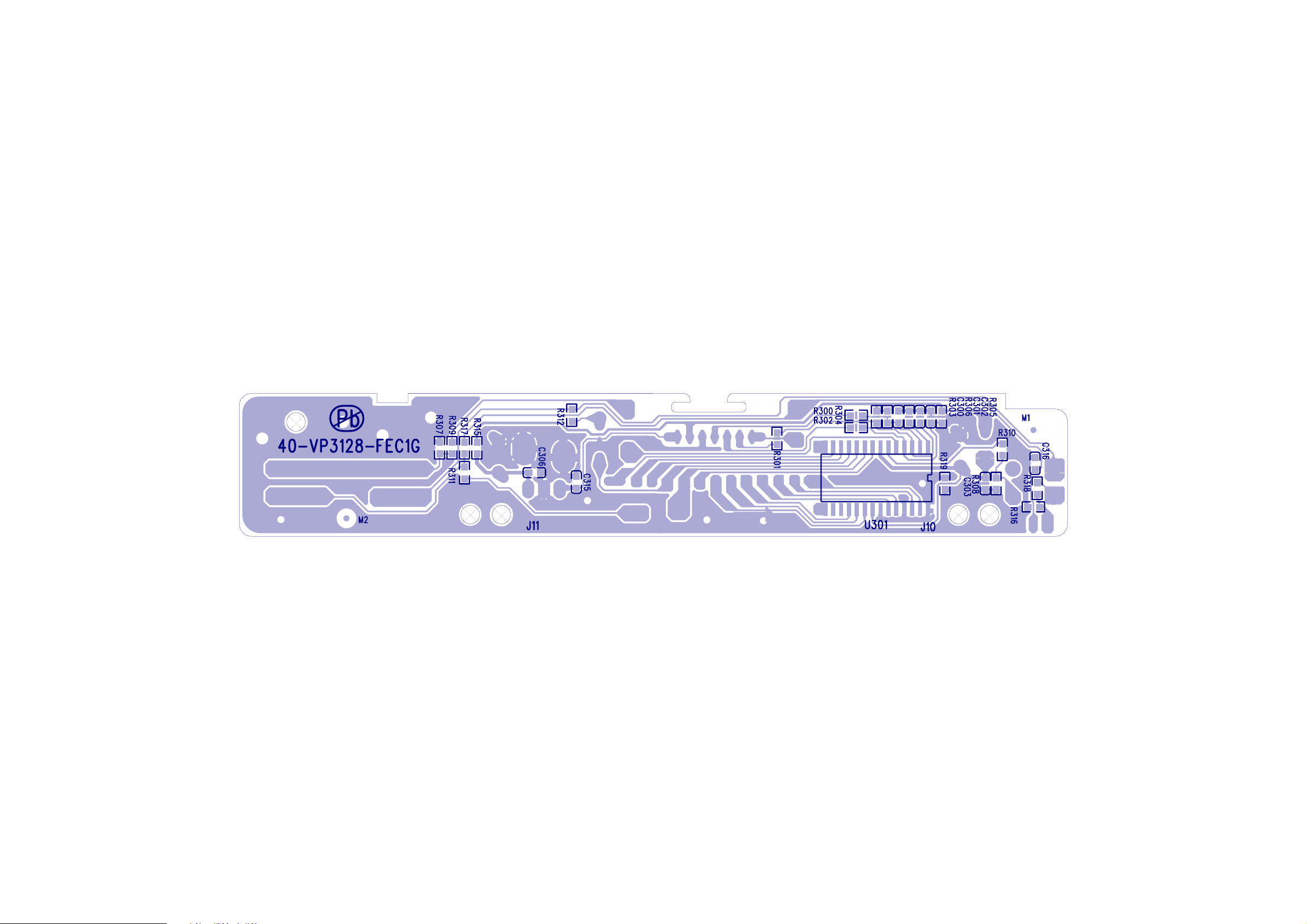
6-9
6-9
Front Board Print-layout (Bottom side)
Page 32
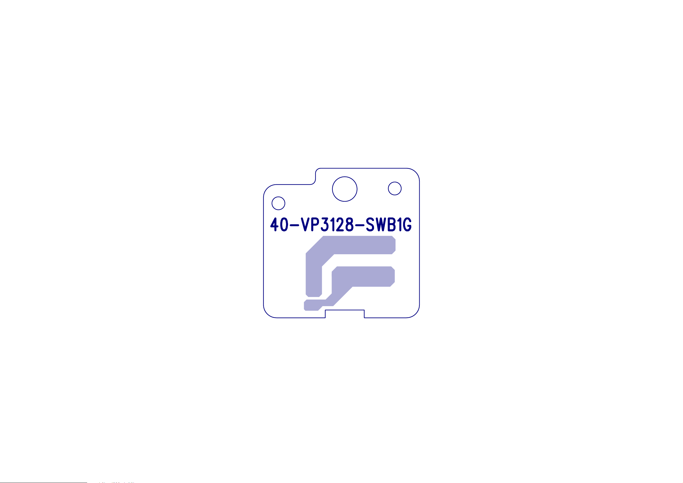
6-10
6-10
Switch Bord Print-layout ( Bottom side )
Page 33
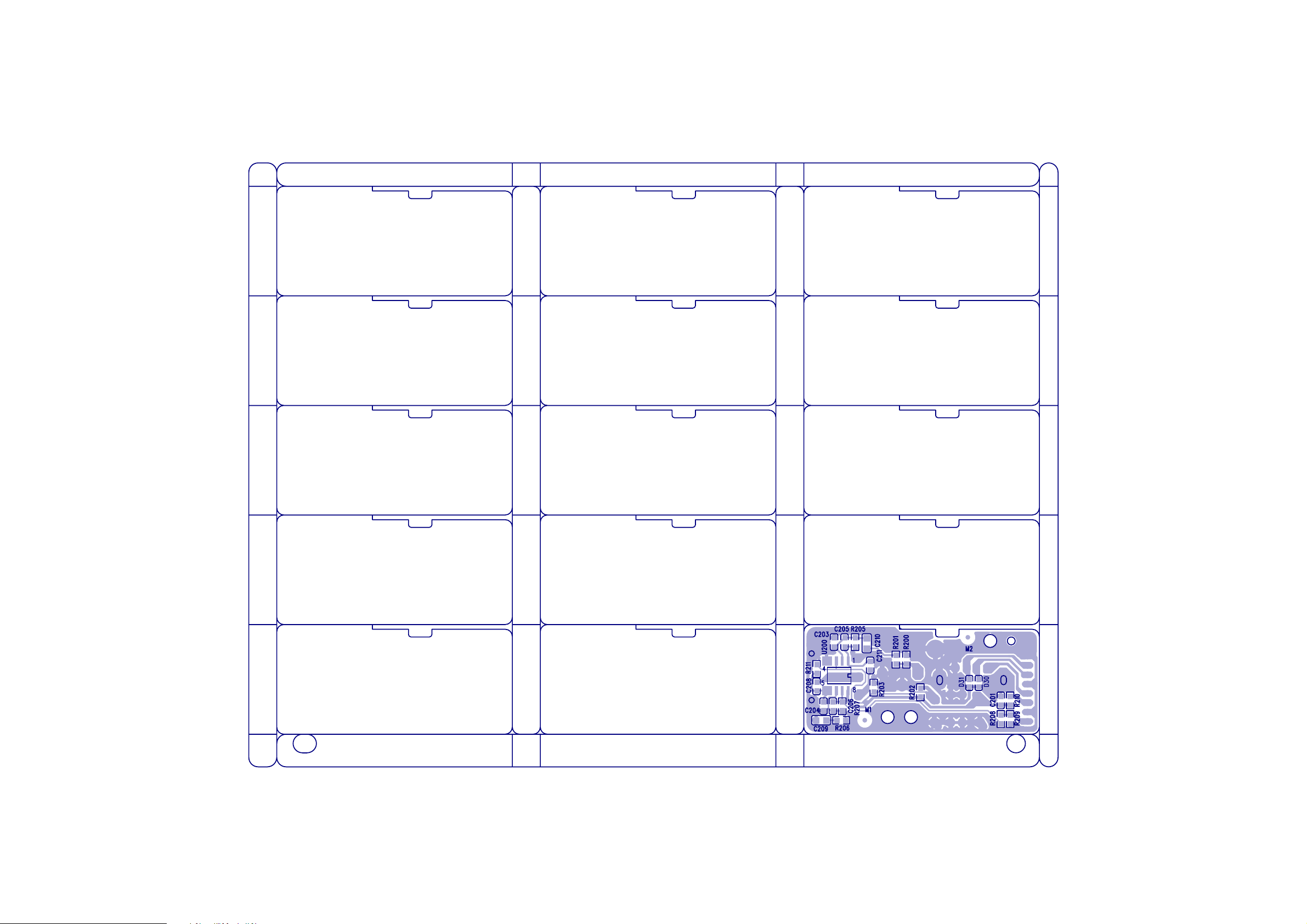
6-11
6-11
OK+USB Board Print- layout (Bottom side )
Page 34
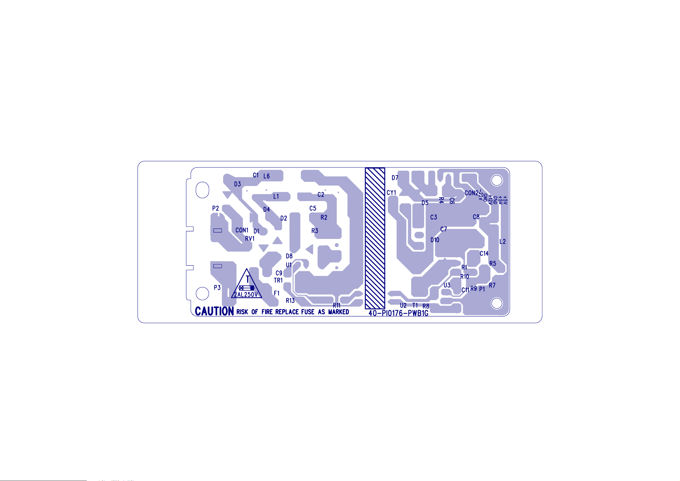
6-12
6-12
Power Board Print-layout (Bottom side )
Page 35
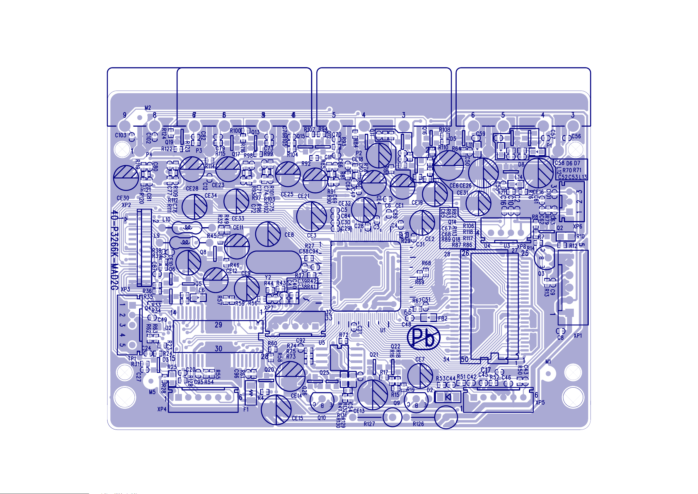
6-13
Main Board Print-layout (Top side )
6-13
Page 36
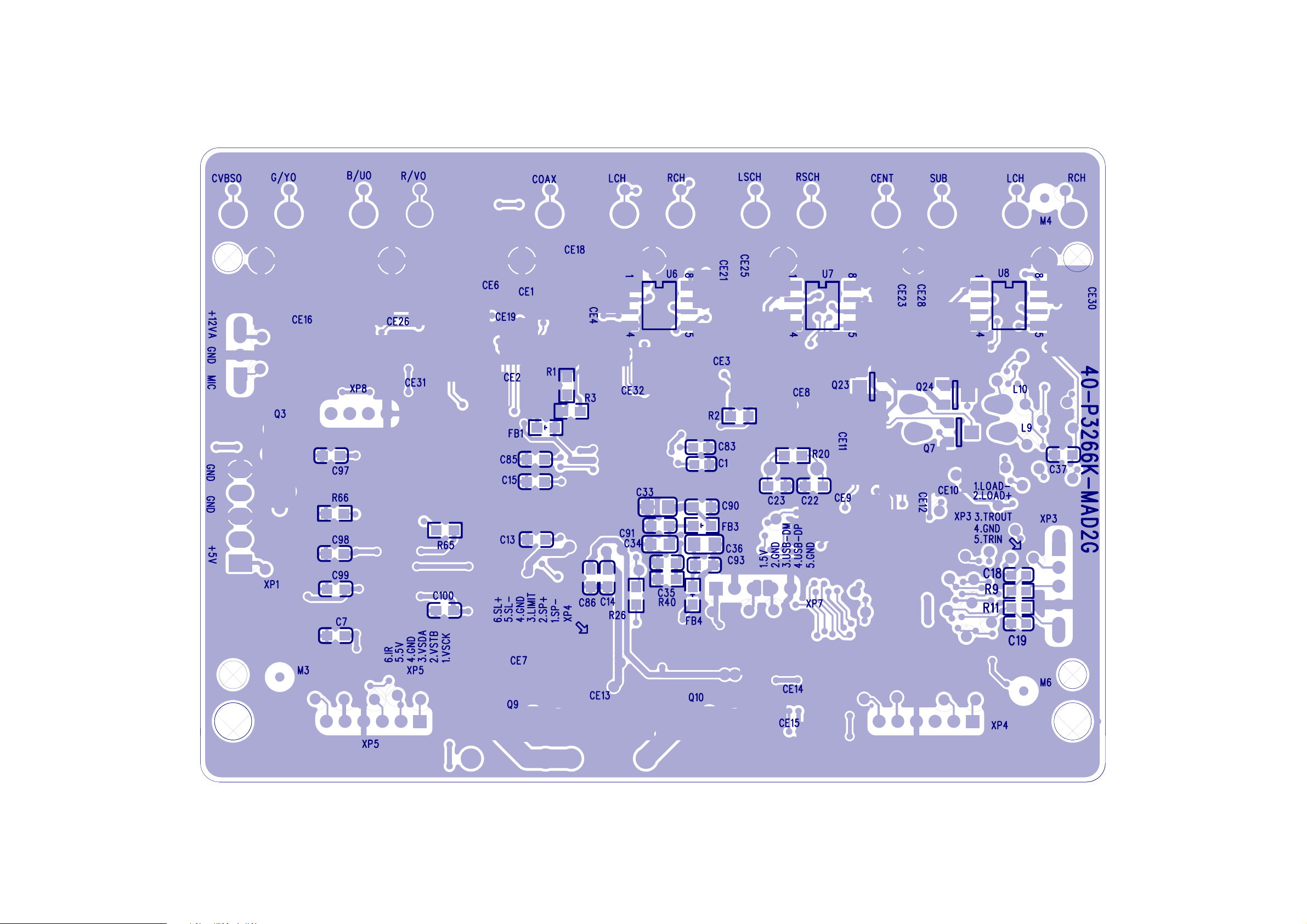
6-14
6-14
Main Board Print- layout (Bottom side )
Page 37
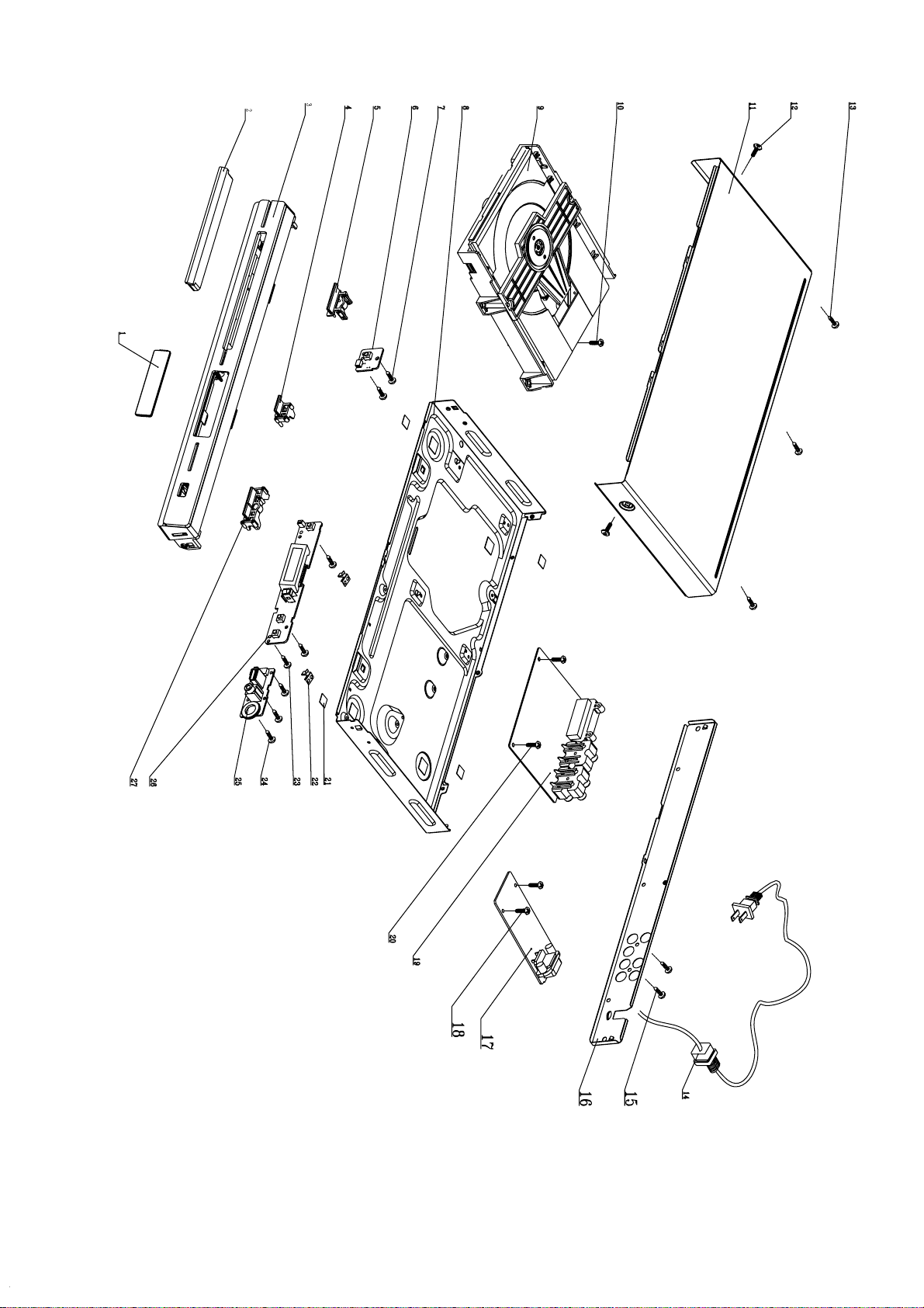
DVP3254K/77 Exploded View
A
7-1
Remark: It's a general view of DVP3254K/77. Please
refer to the model set for the detailed information.
ssy 1 includes components 1.3.4.5.27
Page 38

R
8
R
8
V
5
R
R
7-2
Electrical PARTS LIST MECHANICAL & ACCESSORIES PARTS LIST
No 12NC No. Part Name Q'ty No 12NC No. Part Name Q'ty
17 996510012700 ASSY- PW BD 1 11 996510007452 TOP COVER 1
D1 996510011047 DIODE IN4007 1 14 996510001227 POWER CORD 1
D10 996500027866 DIODE SR360 3A/60V 1 16 996510012699 BACK PANEL 1
D2 996510011047 DIODE IN4007 1 2 996510010963 FRONT DOOR 1
D3 996510011047 DIODE IN4007 1 21 996510006463 PAD 1
D4 996510011047 DIODE IN4007 1 8 996510010966 BOTTOM CABINET 1
D7 996500014043 DIODE FR102 (FAST RECOVERY) 1 AVCable 996510001106 VIDEO CABLE 1500mm 1
D8 996510011047 DIODE IN4007 1 Assy1 996510010964 ASSY - FRONT CABINET 1
L1 996510009942 COIL WIDTH 1 F1 996510001780 FUSE 2A 250V 5X20MM 1
L2 996500032509 COIL SL0811-6R8K2R4 1 RC 996510010959 REMOTE CONTROL 1
T1 996510010954 TRANSFORMER CONV 1 XP1 996510010962 5PIN CBL TJC3-5Y/SCN-5P L=90MM 1
U1 996510010953 IC TNY176PN 1 XP2 996510001168 24PIN HS 1
U2 996500024838 PC123X9YFZ 1 XP3 996510004063 CABLE PH-5Y/PH-5Y L=130MM 1
U3 996500014609 IC AM431LP 1 XP4 996510001222 HS 6P PH-6Y/PH-6Y 1
19 996510010988 ASSY- MAIN BD 1 XP5 996510012698 HS 6P PH-6Y/JC20-6Y 150MM 1
D3 996510009668 BAT54C 1 XP7 996510010961 8PIN CABLE WITCH SHIELD 1
D5 996510009859 SCHOTTKY DIODES BAT54S SOP-23 1 XS302 996510004064 CABLE 2P HS L=160MM 1
D6 996510009859 SCHOTTKY DIODES BAT54S SOP-23 1
D7 996510009859 SCHOTTKY DIODES BAT54S SOP-23 1
D8 996510009859 SCHOTTKY DIODES BAT54S SOP-23 1
L10 996500014082 COIL CHOKE 10UH +/-10% 1
L9 996500014082 COIL CHOKE 10UH +/-10% 1
Q10 996510009671 TRANSISTOR 1
Q11 996510009669 SMD.TRANSISTOR MMBT3904LT1 NPN 1
Q12 996510009669 SMD.TRANSISTOR MMBT3904LT1 NPN 1
Q13 996510010949 MOSFET AO3402 1
Q14 996510009670 TRANSISTOR SMT 3CG9012M 1
Q15 996510009670 TRANSISTOR SMT 3CG9012M 1
Q16 996510009670 TRANSISTOR SMT 3CG9012M 1
Q17 996510009670 TRANSISTOR SMT 3CG9012M 1
Q18 996510009669 SMD.TRANSISTOR MMBT3904LT1 NPN 1
Q19 996510009669 SMD.TRANSISTOR MMBT3904LT1 NPN 1
Q2 996510009669 SMD.TRANSISTOR MMBT3904LT1 NPN 1
Q20 996510009669 SMD.TRANSISTOR MMBT3904LT1 NPN 1
Q3 996510009671 TRANSISTO
Q4 996510009669 SMD.TRANSISTOR MMBT3904LT1 NPN 1
Q5 996510009769 N Channel MOSFET 2SK310
Q7 996510009670 TRANSISTOR SMT 3CG9012M 1
Q8 996510009670 TRANSISTOR SMT 3CG9012M 1
Q9 996510009671 TRANSISTO
QQ6 996510009769 N Channel MOSFET 2SK310
U1 996510010950 IC MT1389DE/L 1
U2 996510009674 IC AM5888IC 1
U4 996510009863 64M SDRAM TSOP54 M12L64164A-7T 1
U5 996510010951 16M FLASH 1
U6 996500032494 IC AS4558M 1
Y2 996510009675 27MCL20PF 1
25 996510010958 KU BD 1
U200 996500032494 IC AS4558M 1
26 996510010956 ASSY- FB BD 1
LED1 996510010957 LED 1
REM3 996510010903 IR RECEIVER MODULE 14MM 5
U301 996510009665 IC ET6202 SOP-2 1
6 99651001095
9 996510005283 DVD LOADE
OPU 996510006029 LOADE
ASSY- SW BD 1
1
1
1
1
1
1
1
Page 39

REVISION LIST
Version 1.0
* Initial release
8-1
 Loading...