

Philips DVDR-985 Schematic

Color Television Chassis
Service
Service
2022
Service
ServiceManual
Contents Contents
1. Technical Specifications 00
2. Safety & Maintenance Instructions, Warnings and Notes 00
4. Mechanical Instructions 00
5. Service Modes, Error Codes and Faultfinding 00
6. Block Diagrams and Testpoints 00
7. Electrical Diagrams and PWB's Diagram PWB
Set Wiring Diagram 1
Set Block Diagram 2
Basic Engine Block Diagram 3
Power Supply (Page 1) Schematic 4 35
Power Supply (Page 2) Schematic 5 35
Display Panel Schematic 6 37
Front AV Panel Schematic 7 39
IR and Standby Panel Schematic 8
Analog Board: All in One 1 Schematic 9 41
Analog Board: All in One 2 Schematic 10 41
Analog Board: Tuner / Dem odulator Schemati c 11 41
Analog Board: In / Out 1 Schematic 12 41
Analog Board: In / Out 2 Schematic 13 41
Analog Board: In / Out 3 Schematic 14 41
Analog Board: Sound Processing Schematic 15 41
Analog Board: Power Supply Schematic 16 41
Analog Board: Converter Schematic 17 41
Analog Board: RGB-YUV Converter Schematic 18 41
Analog Board: Digital In / Out Schem atic 19 41
Analog Board: Fan Control Schem atic 20 41
DVIO Front Board Schematic 21 43
DVIO Board: 1394 Interface Schematic 22 44
DVIO Board: Microprocessor Schematic 23 44
DVIO Board: Fifo & Control Schematic 24 44
DVIO Board: DVCODEC Schematic 25 44
DVIO Board: Audio & Video Output Schematic 26 44
Digital Board: VSM, Buffer Mem & Bit Engine Interface Schematic 27 46
Digital Board: AV Decoder STI5508 Schematic 28 46
Digital Board: AV Decoder Memory 29 46
Digital Board: Video Encoder, Empress 30 46
Digital Board: VIP CVBS Y/C Video Input 31 46
Digital Board: Analog Board Cons. Video In / Output 32 46
Digital Board: Progressive Scan - 1 33 46
Digital Board: Progressive Scan - 2 34 46
Digital Board: Power, Clock, and Reset Audio Clock 35 46
Servo Board 43015: Pre- Processor Schem atic 36 58
Servo Board 43015: MACE3 Schematic 37 58
Servo Board 43015: Driver Schematic 38 58
Servo Board 43015: Decoder / Encoder Schematic 39 58
Servo Board 43015: Power Schematic 40 58
Servo Board 43353: Pre- Processor Schem atic 41 60
Servo Board 43353: MACE3 Schematic 42 60
Servo Board 43353: Driver Schematic 43 60
Servo Board 43353: Decoder / Encoder Schematic 44 60
Servo Board 43353: Power Schematic 45 60
Power Supply CBA (Top View) 46
Power Supply CBA (Bottom View) 47
Display Panel CBA (Top View) 48
Display Panel CBA (Bottom View) 49
Front AV Panel CBA (Top) 50
Front AV Panel CBA (Bottom) 51
Analog Board CBA (Top View) 52
©
Copyrig ht 2001 Philips Consumer Electronics B.V. Eindhoven, The Netherlands.
All rights reser ved. No p art of this p ublication may be reproduced, stored in a
retrieval system or transmitted, in any form or by means, electronic, m echanical,
photographic, or otherwise w ithout the prior permission of Philips.
Published by Philips Consumer Electronics Subject to modification 2005 Nov 03
Analog Board CBA (Bottom View) 53
DVIO Front Board CBA (Top View) 54
DVIO Board CBA (Top View) 55
DVIO Board CBA (Bottom View) 56
Digital Board CBA (T op View) 57
Digital Board CBA (Bottom View) 58
Layout Servo Board 43015: (Top Side) 59
Layout Servo Board 43015: (Bottom Side) 60
Layout Servo Board 43353: (Top Side) 61
Layout Servo Board 43353: (Bottom Side) 62
Layout Analog Board (Testlands Top View) 63
Layout Analog Board (Testlands Bottom View) 64
Layout DVIO Board (Testlands Bottom View) 65
Layout Digital Board (Testlands Bottom View) 66
Test Point Overview Servo Board 43015 67
Test Point Overview Servo Board 43353 68
8. Adjustments 00
9. Circuit Description 00
10. Spare Parts List 00
Diagram PWB

Safety Instructions, Warnings, Notes, and
Service Hints
Safety Instructions
General Safety
Safety regulations require that during a repair:
Connect the unit to the mains via an isolation transformer.
z
Replace safety components, indicated by the symbol h , only by components identical to
z
to the original ones. Any other component substitution (other than original type) may
increase risk of fire or electrical shock hazard.
Safety regulations require that after a repair, you must return the unit in its original condition.
Pay, in particular, attention to the following points:
z Route thewires/cables correctly, and fix them with the mounted cable clamps.
z Check the insulation of the mains lead for external damage.
z Check the electrical DC resistance between themains plug and the secondary side:
1. Unplug themains cord, and connect a wire between the two pins of the mains plug.
2. Set the mains switch to the "on" position(keep the mains cord unplugged!).
3. Measure the resistance value between the mainsplug and the front panel, controls,
and chassis bottom.
4. Repair or correct unit when the resistance measurementis less than 1 MΩ.
5. Verify this, before you return the unit to the customer/user (ref. UL-standard no.
1492).
6. Switch the unit ‘off’, and remove the wire between the two pins of the mains plug.
Laser Safety
This unit employs a laser. Only qualified service personnel may remove the cover, or attempt
to service this device(due to possible eye injury).
Laser Device Unit
Feature Data

z
Type
Semiconductor laser GaAlAs
:
z Wavelength
z Output Power
Beam divergence
z
650 nm (DVD)
:
780 nm (VCD/CD)
:
20 mW(DVD+RW writing)
:
0.8 mW(DVD reading)
:
0.3 mW(VCD/CD reading)
:
60 degree
:
Figure:
Note: Use ofcontrols or adjustments or performance of procedure other than those specified
herein, may result in hazardous radiation exposure. Avoid direct exposure to beam.
Warnings
General
z AllICs and many other semiconductors are susceptible to electrostatic discharges (ESD,
).Careless handling during repair can reduce life drastically. Make sure that, during
w
repair, you are at the same potential as the mass of the set by a wrist band with
resistance. Keep components and tools at this same potential. Available ESD protection
equipment:
Complete kit ESD3 (small tablemat, wristband, connection box, extension cable
and earth cable) 4822 310 10671.
Wrist band tester 4822 344 13999.
z Be careful during measurements in the live voltage section. The primary side of the
power supply (pos. 1005), including the heatsink, carries live mains voltage when you
connect the player to the mains (even when the player is "off"!). It is possible to touch
copper tracks and/or components in this unshielded primary area, when you service the
player. Service personnel must take precautions to prevent touching this area or
components in this area. A "lightning stroke" and a stripe-marked printing on the printed
wiring board, indicate the primary side of the power supply.
z Never replace modules, or components, while the unit is ‘on’.
Laser
z Theuse of optical instruments with this product, will increase eye hazard.
z Only qualified service personnel may removethe cover or attempt to service this device,
due to possible eye injury.
z Repair handling should take place as much aspossible with a disc loaded inside the
player.
z Text below is placed inside the unit, on the laser cover shield:
Figure:
Notes
Dolby
Manufactered under licence from Dolby Laboratories. “Dolby”, “ProLogic” and the double-D
symbol are trademarks of Dolby Laboratories. Confidential Unpublished Works.©1992-1997
Dolby Laboratories, Inc. All rights reserved.

Figure:
Trusurround
TRUSURROUND, SRS and symbol (fig 2-4) are trademarks of SRS Labs, Inc.
TRUSURROUND technology is manufactured under licence frm SRS labs, Inc.
Figure:
Video Plus
“Video Plus+” and “PlusCode” are registered trademarks of the Gemstar Development
Corporation. The “VideoPlus+” system is manufactored under licence from the Gemstar
Development Corporation.
Figure:
Macrovision
This product incorporates copyright protection technology that is protected by method claims of
certain U.S. patents and other intellectual property rights owned by Macrovision Corporation
and other rights owners.
Use of this copyright protection technology must be autorized by Macrovision Corporation, and
is intended for home and other limited viewing uses only unless otherwise authorized by
Macrovision Corporation. Reverse engineering or disassembly is prohibited.

TechnicalSpecifications and Connection
Facilities
General:
Feature Data
Mains voltage
z
120V (90 -140VAC)
:
z Mains frequency
z Power consumption mains
z Power consumption standby
Power consumption low power
z
stand-by
50 Hz - 60Hz
:
32 W (typical, record)
:
< 7 W
:
< 3 W
:
RF Tuner
Test equipment : Fluke 54200 TV Signal generator
Test streams : PAL BG Philips Standard test pattern
System:
NTSC-M (USA/BTSC-Stereo+SAP)
Rf - Loop Through:
Feature Data
z Frequency range
z Gain: (ANT IN - ANT OUT)
45 MHz - 860 MHz
:
-4 dB /±2 dB
:
Radio Interference:
Feature Data
input voltage /3tone method
z
(+40 dB min)
typ. 80 dBμV at 75 Ω
:
Receiver:

PLL tuning with AFC for optimum reception
Feature Data
z Frequency range:
z Sensitivity at 40 dB S/N
45.25 MHz - 860 MHz
:
≥ 60dBμV at 75 Ω (video unweighted)
:
Video Performance:
Channel 25 / 503,25 MHz
Test pattern: PAL BG PHILIPS standard test pattern
Modulation 54 %
RF Level 74 dBV
Measured on YUV-EXT1
Feature Data
z Frequency response:
z Group delay ( 0.1 MHz - 3.3
MHz )
0.5 MHz - 4,00 MHz ± 2 dB
:
0 nsec ± 30 nsec
:
Audio Performance:
Audio-BTSC:
Feature Data
z Frequency responseat audio
cinch output:
z S/N according to DIN 45405,
7,1967
z and PHILIPS standard test
pattern videosignal:
z Harmonic distortion ( 1 kHz, ±
25 kHzdeviation ):
40 Hz - 15 kHz / ± 1,5 dB
:
:
≥ -50 dB unweighted
:
≤ 0.5 %
:
Audio-SAP:
Feature Data
z Frequency responseat audio
cinch output:
40 Hz - 15 kHz ± 1,5 dB
:
z S/N according to DIN 45405,
7,1967
:

and PHILIPS standard test
z
pattern videosignal
≥ -60 dB unweighted
:
z Harmonic distortion (1 kHz):
≤ 0.5 %
:
Tuning
Automatic Search Tuning
Feature Data
scanning time withoutantenna
z
z stop level (vision carrier)
z Maximum tuning error of a
recalled program
z Maximum tuning error during
operation
Tuning Principle
≤ 2,5 min
:
≥ 65dBμV, 75 Ω
:
± 62,5 kHz
:
± 100 kHz
:
Automatic detection
Manual channel activation
Analogue inputs
Audio/video Front Input Connectors
Audio
Feature Data
z Input voltage
z Input impedance
Video - Cinch
Feature Data
2 Vrms
:
>10k Ω
:
z Input voltage
1 Vpp ± 0.1V
:

Input impedance
z
75 Ω
:
Video - YC (Hosiden)
Feature Data
z Input voltage Y
Input impedance Y
z
z Input voltage C
z Input impedance C
1Vpp ± 0.1V (with sync)
:
75 Ω
:
burst 286 mVpp ± {x} dB
:
75 Ω
:
Cinch Audio/video Line Input Rear
Audio (EXT1/2 and EXT3)
Feature Data
z Input voltage
Input impedance
z
Video (EXT2-USA)
2 Vrms
:
>10k Ω
:
Feature Data
z Input voltage
Input impedance
z
1 Vpp ± 0.1V (with sync)
:
75 Ω
:
Yc Input Rear (Hosiden; Ext1-usa)
Connector Kind Value Symbol
1
2
3
4
GND
GND
Input voltage Y 1Vpp ± 0.1V/ 75 Ω (with sync)
Input voltage C Burst 286mVpp ± {x} dB/ 75 Ω
v
v
j
Ypbpr Cinch Input Rear (Ext3)
Feature Data

Input voltage Y
z
1Vpp ± 0.1 (with sync)
:
z Input voltage Pr
z Input voltage Pb
z Input impedance
0.7 Vpp
:
0.7 Vpp
:
75 Ω
:
Video Performance
All outputs loaded with 75 Ohm
SNR measurements over full bandwidth without weighting.
Cvbs Output Rear (Ext2)
Feature Data
z SNR Luminance
z SNR Chrominance AM
SNR Chrominance PM
z
> -65 dB
:
> -65 dB
:
> -65 dB
:
z Bandwidth Luminance
5 MHz ± 1dB
:
Yc Output Rear (Hosiden ; Ext1)
Feature Data
z SNR
z SNR Chrominance AM
z
z Bandwidth Luminance
SNR Chrominance PM
> -65 dB
:
> -65 dB
:
> -65 dB
:
5 MHz ± 1dB
:
Ypbpr Out (Ext3)
Feature Data
z SNR
z
Bandwidth
> -65 dB
:
5 MHz ± 1dB
:
Ypbpr Out (Progressive Scan)
Progressive scan is off during stand-by mode

Feature Data
z Progressive scan resolution
z Output impedance
Output amplitude Y
z
z Output amplitude PrPb
z SNR
z Bandwidth Y
z
z YprPb crosstalk
Bandwidth PrPb
525 lines x 60 frames/second
:
75 Ω
:
700mV (100% white, without sync)
:
700mV (100% level)
:
> 60dB (all channels)
:
> 12 MHz ± 3dB
:
> 6 MHz ± 3dB
:
< -50dB (bandwidth < 10 MHz)
:
Audio Performance
Cinch Output Rear (Ext1/2)
Feature Data
Output voltage 2channel mode
z
z Output voltage 5.1 channel
Dolby
z Channel unbalance (1kHz)
Crosstalk 1kHz
z
z Crosstalk 20Hz-20kHz
z Frequency response 20Hz-
20kHz
z
z Dynamic range 1kHz
z Dynamic range 20Hz-20kHz
z Distortion and noise 1kHz
z
20kHz
Signal to noise ratio
Distortion and noise 20Hz-
2Vrms ± 1.5dB
:
1.41Vrms ± 1.5dB
:
<0.85dB
:
>105dB
:
> 95dB
:
± 0.1dB max
:
>100 dB
:
>90dB
:
>88dB
:
>90dB
:
>80dB
:
z Intermodulation distortion
z Phase non linearity
>87dB
:
± 1( max.
:

Level non linearity
z
± 0.5dB max.
:
z Mute (spin-up, pause, access)
z Outband attenuation:
>100dB
:
> 50dB above 25kHz
:
Cinch Output Rear (Ext3)
Feature Data
z Output voltage 2channel mode
z Output voltage 5.1 channel
Dolby
z Channel unbalance (1kHz)
Crosstalk 1kHz
z
z Crosstalk 20Hz-20kHz
z Frequency response 20Hz-
20kHz
z
Signal to noise ratio
2Vrms ± 1.5dB
:
1.41Vrms ± 1.5dB
:
<0.85dB
:
>105dB
:
> 95dB
:
± 0.1dB max
:
>100 dB
:
z Dynamic range 1kHz
z Dynamic range 20Hz-20kHz
z Distortion and noise 1kHz
Distortion and noise 20Hz-
z
20kHz
z Intermodulation distortion
z Phase non linearity
z
z Mute (spin-up, pause, access)
z Outband attenuation:
Level non linearity
Digital Output
>90dB
:
>88dB
:
>90dB
:
>80dB
:
>87dB
:
± 1( max
:
± 0.5dB max
:
>100dB
:
> 50dB above 25kHz
:
Coaxial Output
Feature Data

CDDA/LPCM(incl. MPEG1)
z
According IEC958
:
z MPEG2, AC3 audio
z DTS
According IEC1937
:
According IEC1937
:
Optical output
Identical to coaxial
Digital Video Input/output (Iee1394)
Applicable Standards
Implementation according:
IEEE Std 1394-1995
IEC 61883 - Part 1
IEC 61883 - Part 2 SD-DVCR (02-01-1997)
Specification of consumer use digital VCR’s using6.3 mm magnetic tape - dec.1994
Mechanical connection according:
Annex A of 61883-1
Audio Quality
Feature Data
Output voltage 2channel mode
z
z Channel unbalance (1kHz)
z Crosstalk 1kHz
z Crosstalk 20Hz-20kHz
Frequency response 20Hz-
z
12kHz
z Signal to noise ratio
z Dynamic range 1kHz
z
z Distortion and noise 1kHz
z Distortion and noise 20Hz-
20kHz
Dynamic range 20Hz-20kHz
2Vrms +/- 1.5dB
:
Tbd
:
> 95 dB
:
> 85 dB
:
+/- 1dB max
:
>95 dB
:
Tbd
:
Tbd
:
>65dB
:
>65dB
:

Intermodulation distortion
z
>80dB
:
z Phase non linearity
z Level non linearity
z Mute (spin-up, pause, access)
Outband attenuation
z
+/- 1 degree
:
Tbd
:
Tbd
:
Tbd
:
Dimensions And Weight
Feature Data
z Height of feet
z Apparatus tray closed
z Apparatus tray open
Weight without packaging
z
z Weight
12 mm
:
WxDxH :435 x 325 x 107
:
WxDxH :435 x 465 x 107
:
5.670 g
:
1.675 g
:
Laser Output Power & Wavelength
DVD
Feature Data
Output power duringreading
z
z Output power during writing
z Wavelength
CD
Feature Data
z Output power
Wavelength
z
0.8mW
:
20mW
:
660nm
:
0,3mW
:
780nm
:

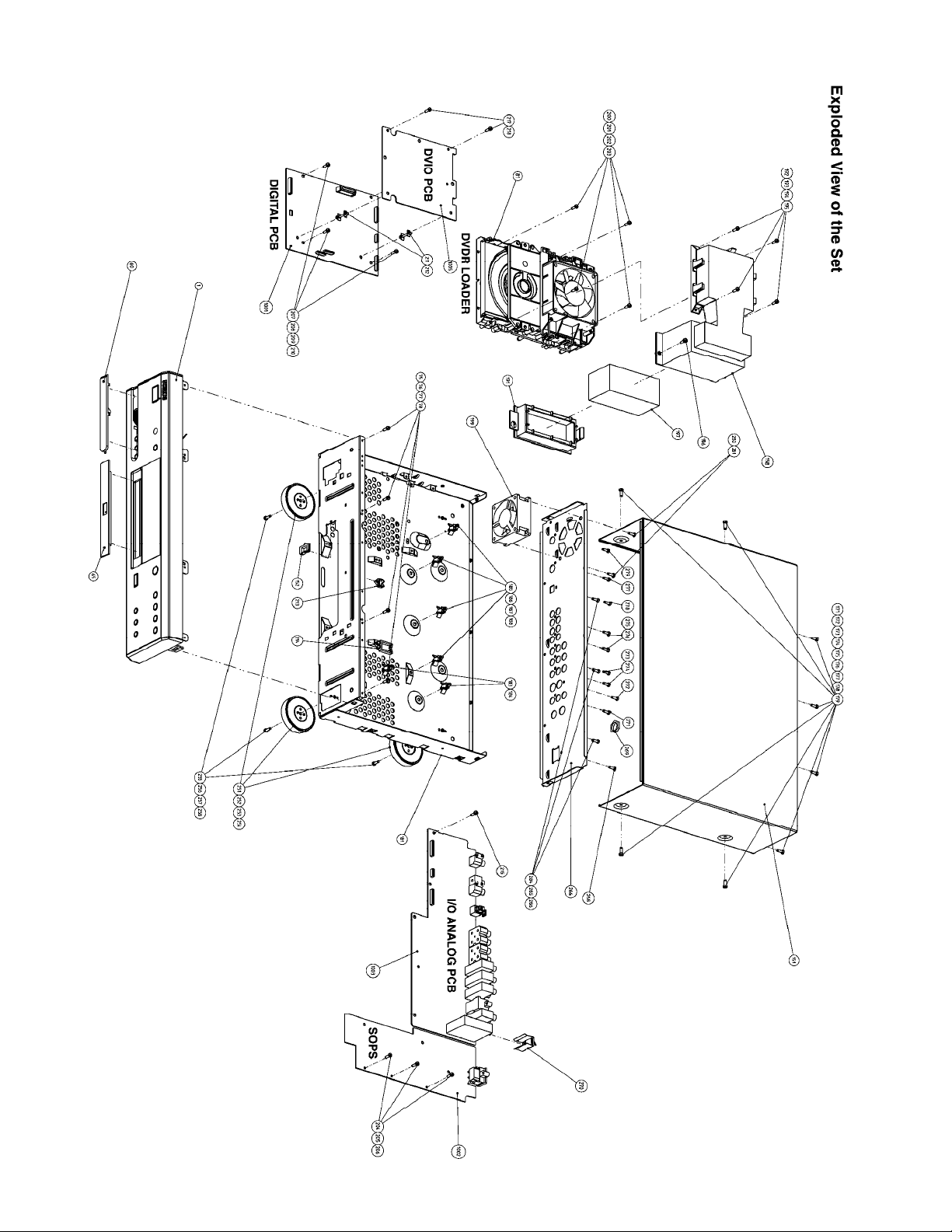
Complete Set Exploded View

Front Assembly ExplodedView

Basic Engine Exploded View
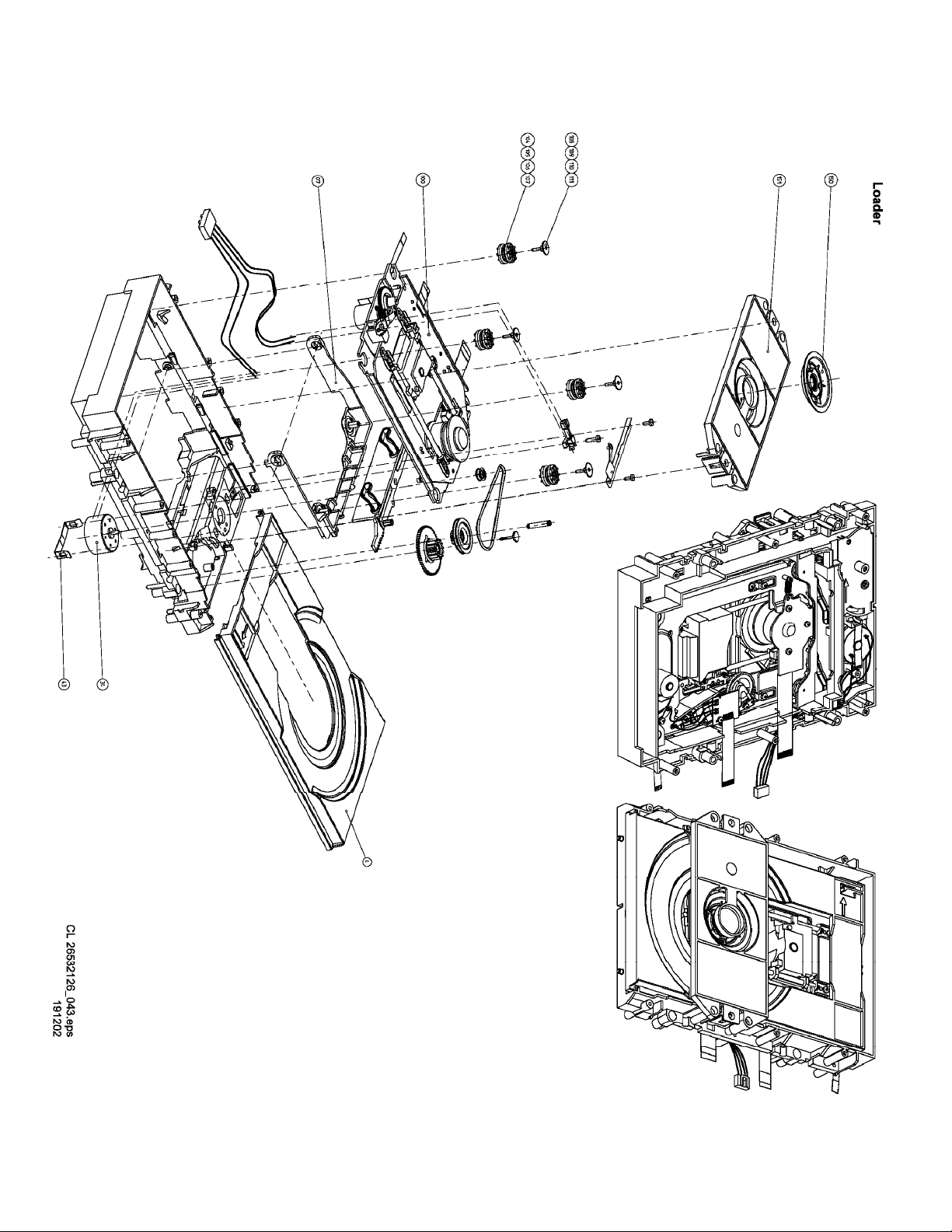
Loader Exploded View

DVM Exploded View


(2022)
Vdrain(stby) Vdrain.tif Vgate(stby). Vgate.tif
Vsource(stby Vsource.tif

Alignments
Alignment Instructions analog Board
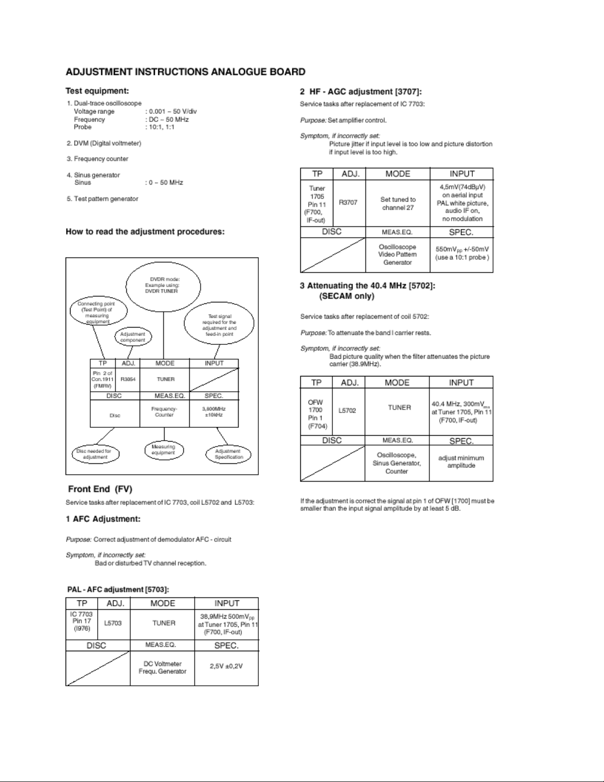

Figure: Alignments Analog PCB Eur
Reprogramming Procedure of NVM on the analog PCB
The NVM, item 7815, on the analog board contains the following factory settings:
1. Bargraph 0dB correction factor
2. Clock correction factor
3. AFC reference value
4. Slash version
The settings 1,2 and 3 are stored in the NVM during the production of the analog board.
The slash version is stored at the end of the production line of the set.
In case of failure, the NVM must be replaced by an empty device. By way of commands via the
Diagnostic Software or via ComPair, the factory settings must be restored in the NVM.
Bargraph 0db Alignment
For an exact functionality of the bar graph in the display, a correction factor for the left and the
right channel is stored in the NVM.
Procedure:
z Put the setin DSW command mode
z route Audio path from Audio front connectors to digital with the following command: DD:>
713 01
z apply a sine wave of 1 kHz, 1.65 Vrms (0 dB)to the front connectors, audio left and right
z store 0 dB bar graph level with command 720DD:>720
Clock Correction Adjustment
To guarantee an exact function of the real time clock, an adjustment of the clock frequency is
possibe and stored in the NVM.
Procedure:
Connect a pull up resistor of 10k between pin 7 an 8 of the clock IC PCF8593T,item
z
7811, on the analog PCB
put the set in service command mode
z
execute command 722 to initiate that a 1 Hz signal is available on pin 7 of the clock
z
ICDD:>722

z measure the frequency of the Clock Crystal with an accuracy of ±1(s. Normally the
measured frequency must be between 999902 (s and 1000097 (s. If the frequency is
outside this range, the clock IC must be replaced.
z Execute command 721 with the measured frequency as an input parameter
example:DD:>721 1000023
AFC Reference Voltage Tuner
This function stores the reference voltage for the tuner in the NVM. Before this value can be
stored, the AFC adjustment, described in the adjustment instructions of the analog board, must
be carried out.
Procedure:
z Adjust AFC circuit
z Calculate the reference value
z Execute command 732 and use the calculated reference value as parameter
example:DD:>732 128
Slash Version
The slash version is stored with command 715 followed by the slash version as parameter.
The slash versions used in DVDR1000 and DVDR1500 are the following:
DVDR980/17X: 103
z
DVDR985/17X: 104
z
Example:
DD:>715 1
Reset of Slash Version
Use command 729 to reset the analog board to the default setting.
Procedure:
z Put the setin DSW command mode
z Execute command 729 with the following parameters: DD:> 729w 0xA0 3 0x07 0xD0
0x00
z Leave the DSW command mode and start up the set in application mode No background
is visible on the TV screen. The analog board is ready to accept the appropriate slash
version.

Rework ProcedureIEEE Unique Number
Scope:
The procedure describes how to upgrade sets with a unique number after repair. This unique
number is stored in the NVRAM (item 7201) of the digital board at the end of the production
line.
This procedure is only valid or necessary when:
z The digital board is replaced
z NVRAM on the digital board is replaced
z NVRAM is cleared
In all other cases the repaired set retains its unique number.
The procedure defines several means to re-assure the unique number, depending on the
possibilities of repair or the state the faulty set is in.
Handling:
State of Original (Defective) Board:
1. The digital board starts up in Diagnostics Mode: follow procedure A to retrieve the valid
unique number
2. The digital board does NOT start up in Diagnostics Mode: follow procedure B.
Procedure A
1. Connect defective digital board to PC via serial cable (3122 785 90017)
2. start up hyper terminal or any other serial terminal via the correct settings (DSW
command mode interface)
3. read out existing unique number via nucleus 403 example:DD:> 40340300: DV Unique
ID = 00D7A1FC6CTest OK @
4. note read out
5. program new digital board via nucleus 410 example: DD:> 410 00D7A1FC6C41000:Test
OK @
The set has now the original unique number
Procedure B

1. Notethe serial number of the set example: AH050136130156
AH = production center Hasselt. According to UAW-500: A=1 and H=8
05 = change code (this is not used for this calculation)
01 = YEAR
36 = Production WEEK
130156 = Lot and SERIAL number
2. Calculate the unique number: this number always exists out of 10 hexadecimal numbers.
3. First 5 numbers: First we calculate a decimal number according to the formula below:
35828*YEAR + 676* WEEK + 26*A + H + 8788The figures are fixed, YEAR + WEEK +
factory code( A + H) are variable Example: 35828*01+676*36+26*1+8+8788 = 68986
(decimal)Then we translate the decimal number to a hexadecimal number.example:
68986 (decimal)= 10D7A (hex)
4. Last 5 numbers: The last 5 numbers exist out of the Lot and SERIAL number. We have
to translate the decimal number to the next 5 hexadecimal numbers: Example: 130156
(decimal) = 1FC6C (hex)
5. Program new digital board via nucleus 410 Therefore we use the 10 hexadecimal
numbers we calculated above: example:DD:> 410 10D7A1FC6C41000:Test OK @
The set has now its original unique number

Mechanical, and Dismantling Instructions,and
Exploded Views
Service Positions
Front
Figure: Front
DVIO Board
To put the DVIO board in a service position,an extender board must be used. This extender
board can be orderedwith codenumber 3104 128 07770.

Figure: DVIO Extender
Figure: DVIO 1
 Loading...