Philips DVDR-75 Service manual
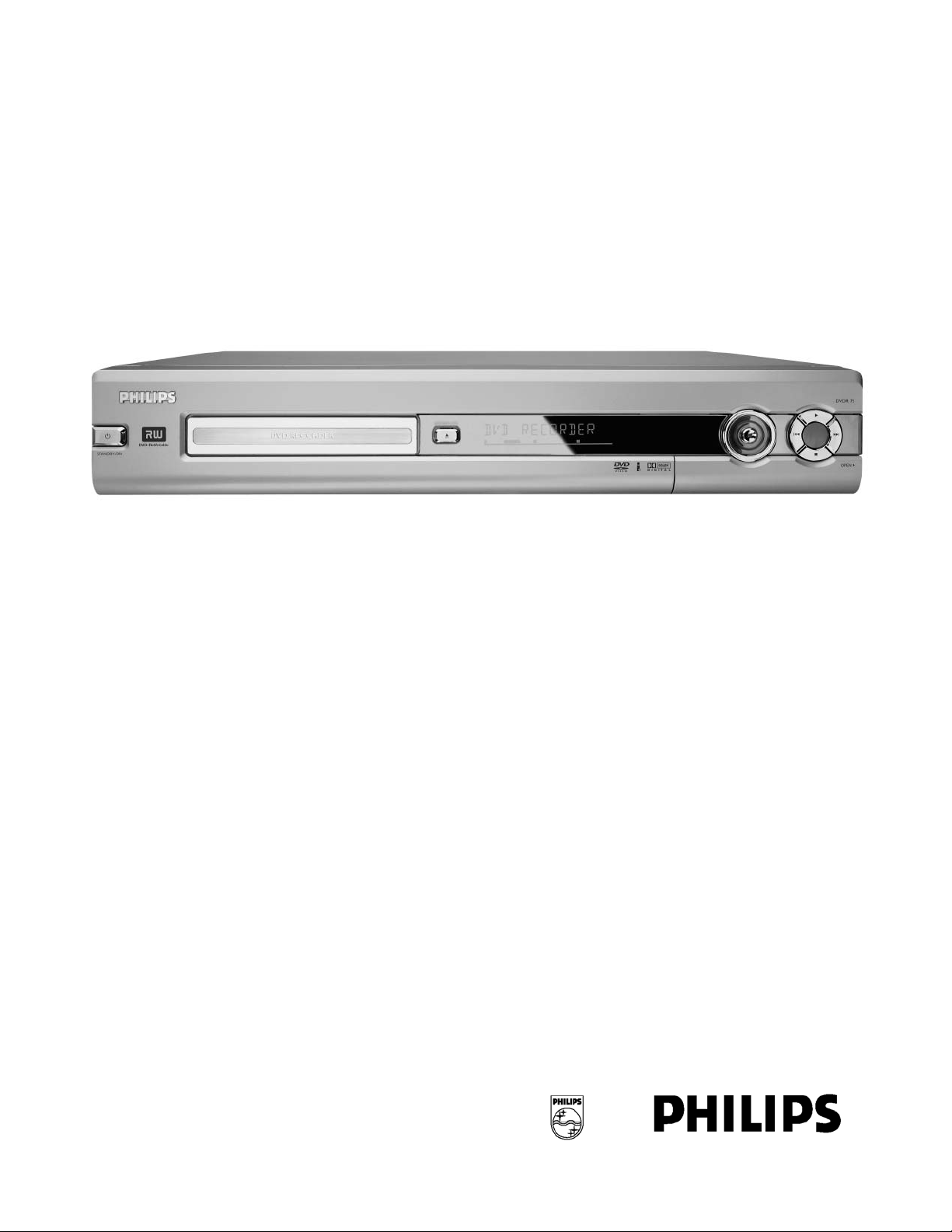
Philips DVDR75
Technical Training Manual
Philips Service and Quality/Training
One Philips Drive
Knoxville, TN 37914-1810
P. O. Box 14810
PH: 865-521-4397
FAX: 865-521-4818
EMAIL: TECHNICAL.TRAINING@PHILIPS.COM
Introduction
This manual is intended for use by the Service
Technician. There are two versions of the
DVDR75. The first four digits of the Product
Number indicates the version. The Product
Number is similar to a Serial Number. It will read
VN02 or VN04. The VN04 is the newer of the
two. The VN04 uses an updated Digital Board
that contains the functionality of the DVIO Board.
When there are two versions of a circuit, the title
to the section will have one or the other in the
title, VN02 or VN04.
The first portion of this manual contains a basic
description of disc based data playback and
recording technologies. Self Diagnostics are
included to aid in troubleshooting. Technical
Descriptions of the circuitry are followed by a
Troubleshooting Section.
The DVDR75 is the forth generation in a line of
DVD recorders. Recordings can be made from
broadcast transmissions, and from other analog
or digital sources. The DVDRW format allows
the user to record and erase a disc many
times. The recorded discs will play on most
existing and future DVD players. The DVDR75
has a connection for DV or Digital camcorders
via an I-Link or Firewire connection. This connection technically is called an IEEE 1394 connection. This machine records on 4.7Gbyte
DVD+R and DVD+RW discs. This machine
uses a real-time MPEG2 Variable Bit Rate,
VBR, Video encoder. The DVDR75 plays back
DVD Video, Video CD, Audio CD, CD-R, and
CD-RW discs.
Its many features include: Favorite Scene
Selection for easy editing, Index Picture Screen
for instant overview of contents, Digital Time
Base Corrector, Digital Audio output (DTS, AC3, MPEG, PCM), TruSurround for 3D sound,
Zoom + Perfect Still. It is Widescreen, 16:9
compatible, and has a Universal Remote
Control, 20 disc resume, Disc Lock, and One
Touch Recording.
Virgin Mode
The DVDR75, when first hooked up, needs to
get information from the user about what language and what local broadcast system the unit
is going to operate with. Use the remote to make
those selections. The unit will not operate until
this process is completed. If you want the
recorder to start up in Virgin mode, unplug the
recorder. Plug the recorder in again while holding the STANDBY-ON button.
DVD Basics
Philips with nine other manufacturers chose a
format specification for DVDR and RW on March
16, 2001. This format uses Real Time recording.
Its recording is compatible with DVD-Video, and
DVD ROM. The data blocks use lossless linking.
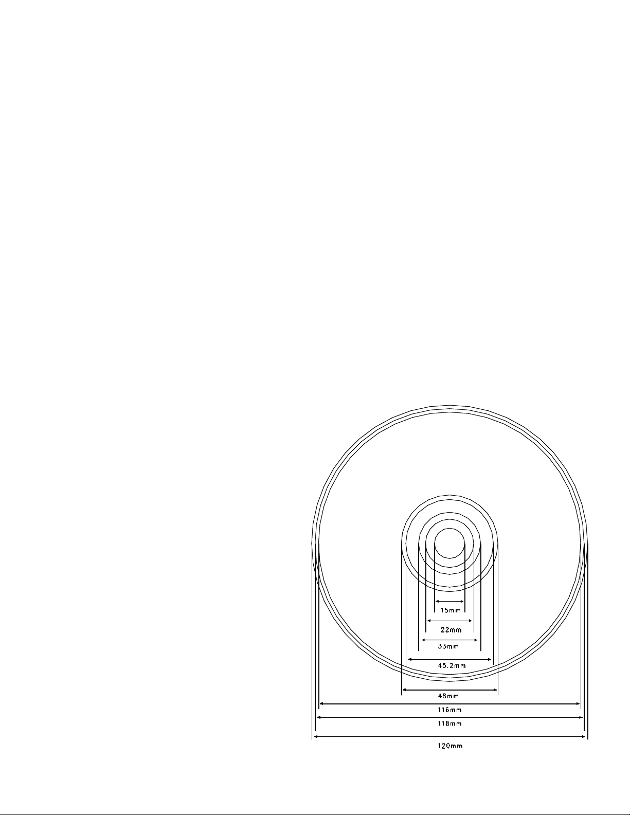
The physical layout matches very closely to that
of a DVD ROM. See Figure 1. It also uses
Direct Overwrite when a RW disc is used.
Figure 1 – DVD ROM Disc
1
Laser Technology
The DVD and CD share much of their technology. We will start with CDs and work our way to
the DVD. CDs use a red laser created by a
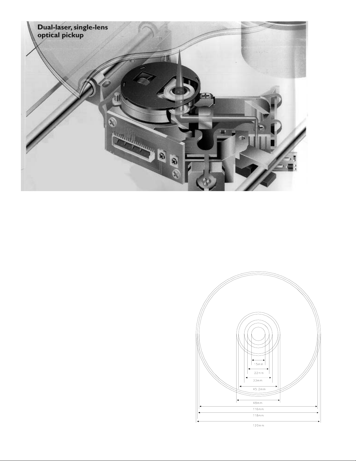
diode and lens system often called a Light Pen.
Refer to Figure 2. The narrow beam of light is
focused onto the reflective layer of a disc. At the
instant that focus is achieved, the disc is spun.
The laser starts on the innermost tracks of the
CD and reads outward. At the beginning of the
disc is the Table of Contents. At the bottom of
the Light Pen are Monitoring Diodes. The
Monitoring Diodes provide information about
focus and tracking. Data is retrieved from the
disc in the form of pulses of light reflecting from
the disc. The pulses are created by Pits in the
Reflective Layer of the disc. The Pits reflect less
light than the intact surface of the Reflective
Layer, called Lands. The data is binary. A 1 is
generated when the light transitions from bright
to dim and dim to bright. The time between is a
series of zeros determined by the data rate.
Disc Mechanical Layout
The CD is a plastic disc 120mm in diameter, with
a thickness of 1.2mm. Refer to Figure 3. It has
a silver colored Reflective Layer. The maximum
playing time for a music recording on a Compact
Disc, CD, is 74 Min.
Figure 2 – CD Laser Operation
2
Figure 3 - CD Disc
The CD is less vulnerable to damage than an
analog record. That does not mean it does not
have to be treated with care. Dirt and heavy
scratches can interfere with playability.
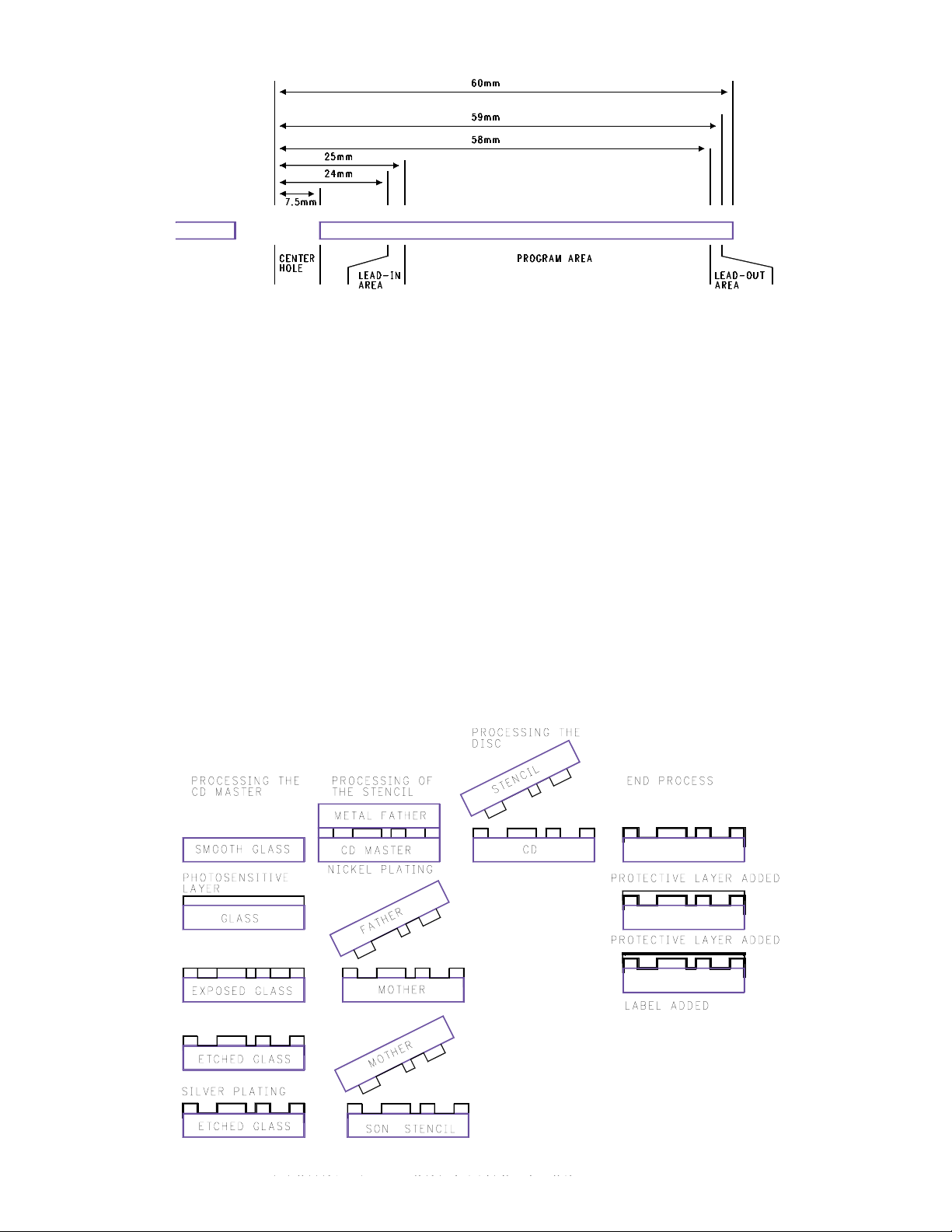
As shown in Figure 4, the CD is subdivided into
three parts: the Lead In Track, the Program
Area, and the Lead Out Area. These three sections together are considered the Information
Area. There is a hole in the center for holding
the disc. The disc is held between two equally
sized concentric rings. The rings have an inner
diameter of 29mm and an outer diameter of
31mm.
The Data on the disc is recorded on a spiral
shaped track with pits and lands. The reflective
side of the disc contains the tracks.
The production of a disc is a high tech process
explained in Figure 5. The process starts with
glass that is photo etched. The glass is silver
plated and is used as a form for a metal cast.
The metal cast is used to stamp a nickel Mother
Stencil. The Mother Stencil is used to stamp the
Son Stencil. Son Stencils are used to stamp the
foil of the discs. A protective layer and label are
added.
Figure 4 - The Disc
Figure 5 - Creating a CD
3
Read Process
The Servo circuit is responsible for focusing the
laser and moving the Light Pen to follow the spiraling tracks on the rotating disc. The digital High
Frequency information, HF, is demodulated and
stored in RAM. When the RAM is half full, the
data is fed out to the Digital to Analog Converters.
The speed of the rotating disc is servo controlled
to keep the RAM half full. The analog signals are
amplified and sent to the output connectors.
Record Once Technology
Disc Mechanical Layout
From an external point of view, a DVD is the
same as the CD. Recordable media creates the
need for three physical layouts. There are three
possible states of a disc: a blank disc, a partially
recorded disc, and a full or finalized disc. The
difference is in the way the Information Area is
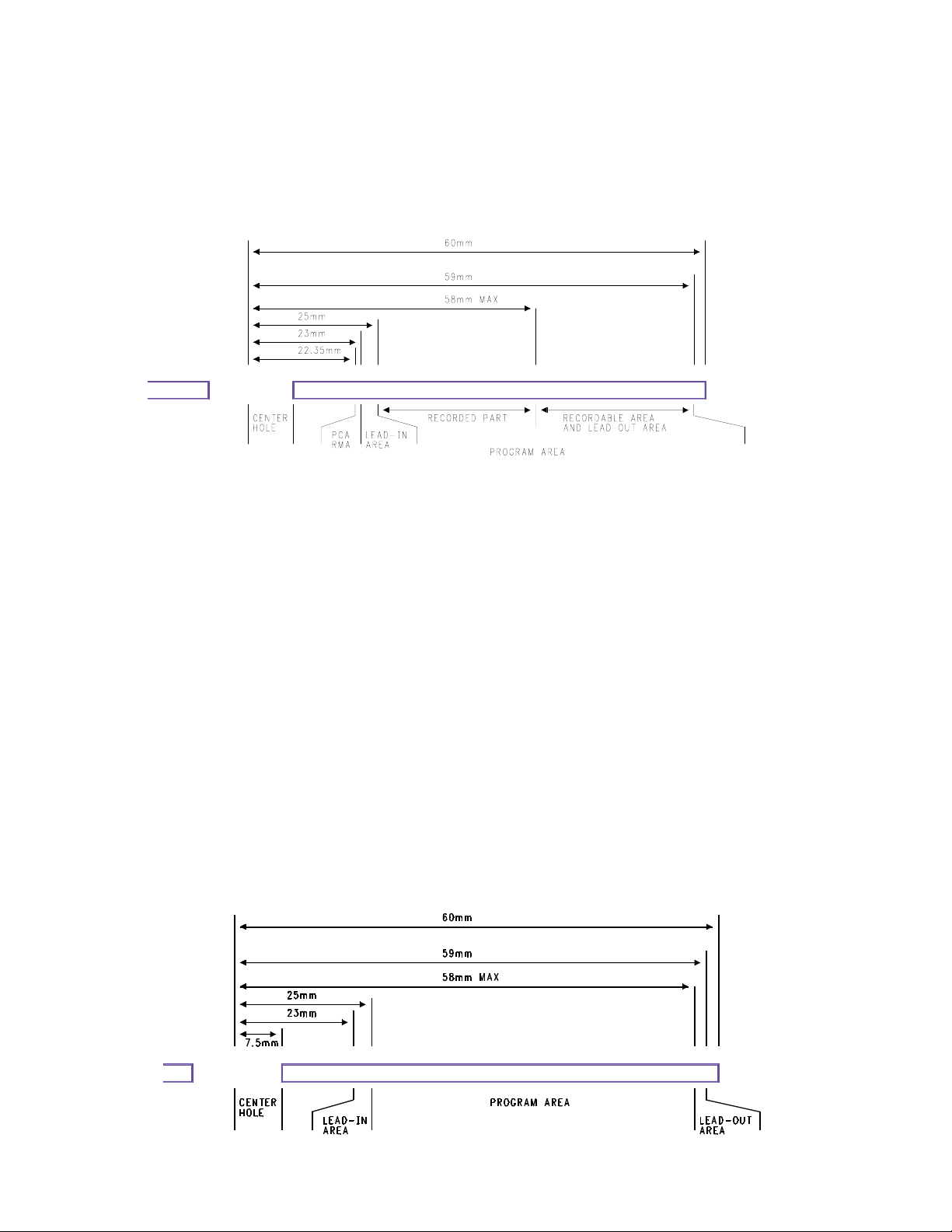
divided. The Information Area of a blank disc
extends from 22.35 mm centered on the disc to
59 mm centered on the disc. Refer to Figure 6.
A partially recorded disc’s Information Area has
four sections: a PCA/RMA area, a Lead In Area,
a Recorded Program Area, and a Recordable
Program Area. See Figure 6 for the dimensions.
The PCA Area is the Power Calibration Area,
PCA. The RMA Area is the Recording
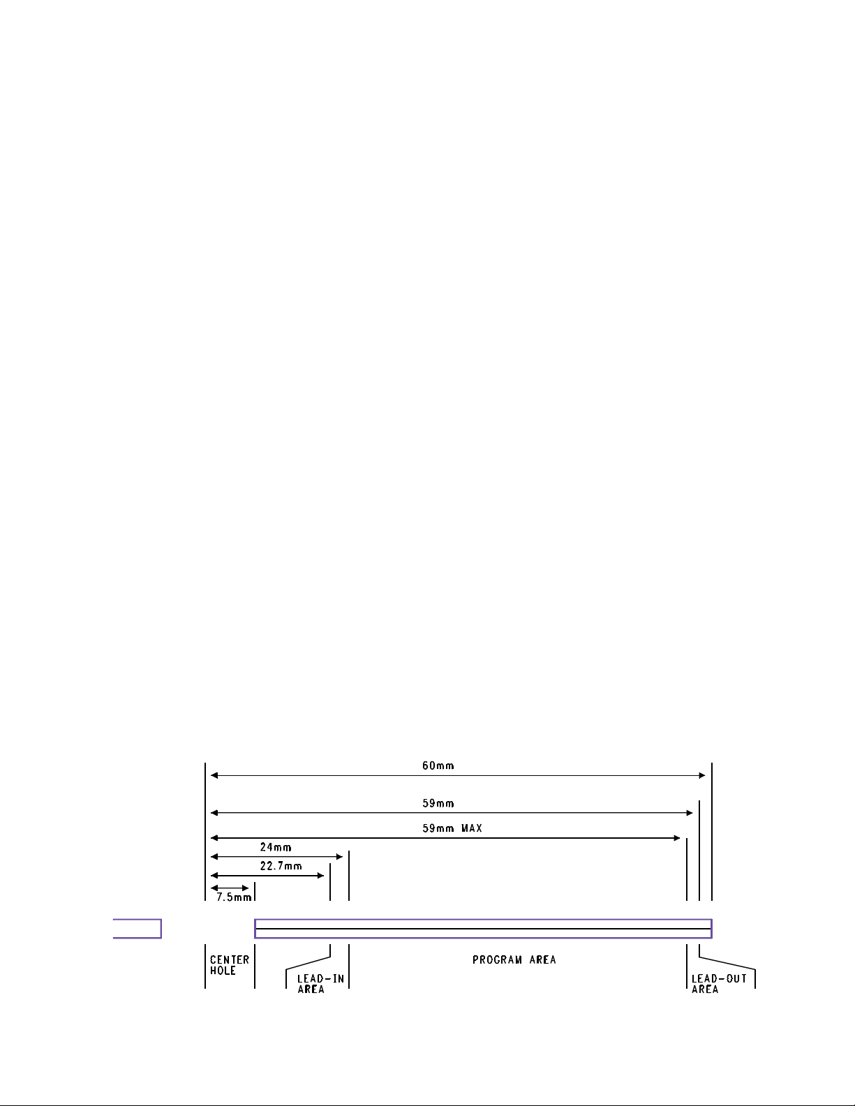
Management Area. A fully recorded or finalized
disc’s Information Area has three sections: A
lead in Area, the Program Area, and the Lead
Out Area. See Figure 7 for the dimensions.
The disc’s recordable layer contains major differences from that of a stamped disc. The blank
disc has a Pre-groove stamped into the recordable layer of the disc. This is polycarbonant for
DVD+Rs and organic dye material for
DVD+RWs. This spiral Pre-groove is for the
Servo circuit to provide a mechanical reference
during recording. The dye based RW recordable
layer provides a reflectivity of 40% light return
and 70% light return. 40 percent reflectivity represents Pits and the 70% represent the Lands.
Record Process
The record process shares most of its mechani-
Figure 6 – A Partially Recorded Disc.
Figure 7 – Fully Recorded or Finalized Disc
4
cal operation with that of the play process. The
main difference is how the Servo is locked to the
disc. The Servo follows the Pre-groove for Radial
Tracking and disc speed. The speed of the disc
is locked to a wobble signal that is part of the
spiral grove stamped into the disc.
The intensity of the laser beam is modulated
from playback intensity to write intensity. As the
disc reads the Pre-groove, the laser arrives at a
position where a Pit is to be formed. The laser
power increases from 4mW to 11mW. This raises
the temperature of the disc to 250 degrees
Celsius. The recordable layer melts, reducing its
volume. The polycarbonate flows into the space
vacated by the dye. The modulation from read
laser power to write laser power forms a pit and
land pattern effectively the same as a prerecorded disc.
Re-recordable Technology
Disc Mechanical Layout
Disc usage mechanically is identical to the
recordable media. The only difference is the
chemical make up of the recordable layer. The
recordable layer is made up of an alloy of silver,
indium, antimony and tellurium.
Re-Recording Process
The Re-Record process shares much of its operation with that of a CDR. The blank disc’s
Information Area is in a polycrystalline state.
During recording, the laser power is modulated
from 8mW to 14mW. 8mW is the playback laser
power and 14mW is the record laser power. The
polycrystalline state of the recordable surface
changes, or melts at 500-700 degrees C into an
amorphous state. The melted, amorphous areas
reflect light less than the crystalline areas, creating a pattern similar to the stamped CD. A major
difference of CDRWs from CDRs is the ability to
erase.
The Erase Process
To Erase a CDRW disc, the recordable layer
must be returned to its polycrystalline state. This
is done by heating up the temperature of the
recorded surface to 200 degrees C. This is less
than the melting point. This is done at X2 recording speed. The slower speed allows time for the
alloy to return to its proper state. This takes
approximately 37 min. Some software erases the
just the TOC on the disc and allows the disc to
be rewritten. This method is not as reliable
Over Writing Process
Over writing combines the processes of erasing
and writing. When the disc and Light Pen are in
position to start writing the new data, the laser
power starts modulating in the same manner as
it does for normal recording with one difference.
During the time there is to be a land, the laser
power goes to the erase level rather than the
playback level.
Figure 8 – Mechanical Layout of a DVD
5
DVDs
All of the previously discussed technologies
apply to the DVD. Like CDs, DVDs are also
stamped into play only discs. In this discussion,
we will point out the differences between DVDs
and CDs. If you are new to disc based technology, you will want to start with the information preceding this discussion.
DVD Disc Mechanical Differences
Most DVDs are single sided, however, the DVD
specification allows for two readable layers, and
the disc can be double sided. We will start our
discussion with single sided, single layered
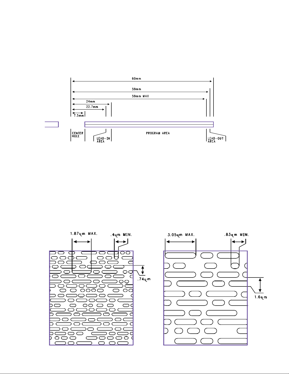
discs. A Digital Versatile Disc, DVD, looks very
similar to a CD. Refer to Figure 8. The Clamping
Area is larger, starting at 11 mm centered to 16.5
mm centered. The Lead In Area is smaller,
measuring 22.7 mm centered to 24 mm centered. The Information Area is limited to 116mm
centered.
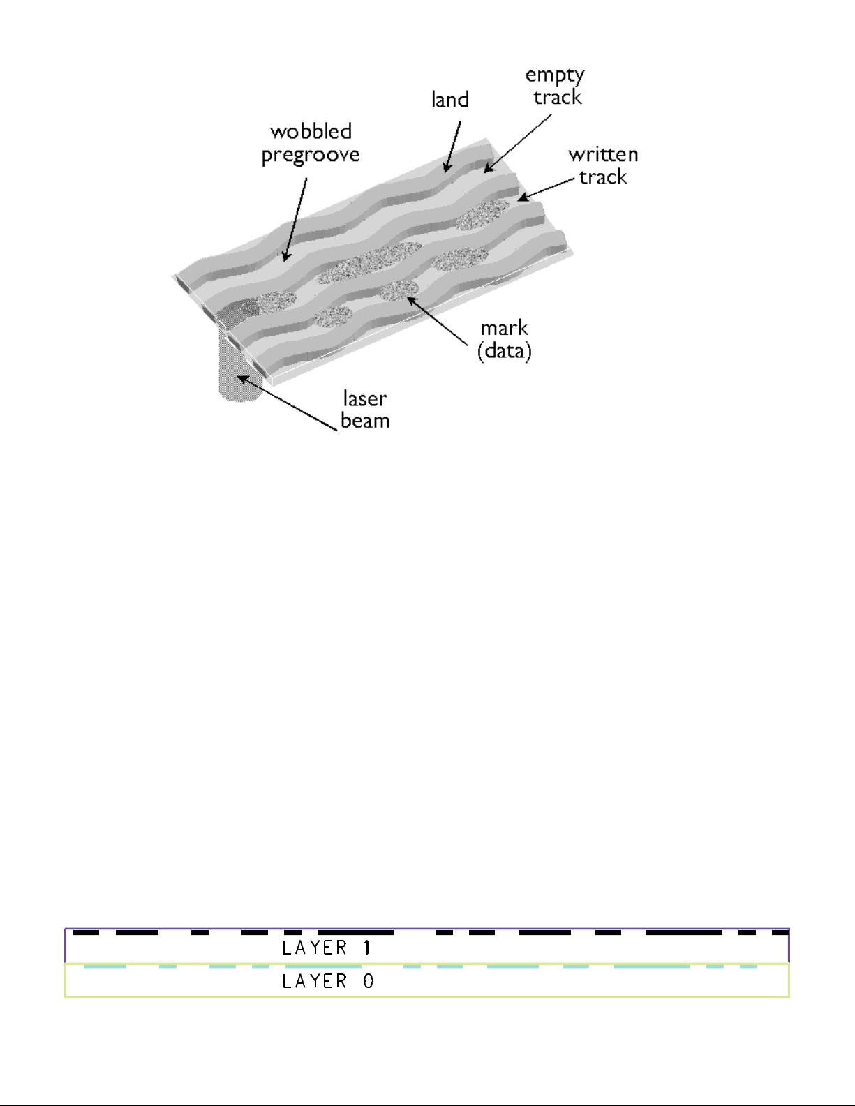
Two of the big differences between DVDs and
CDs are the Pit and Land sizes, and the track
widths. Refer to Figure 9.
The Manufacturing process of a DVD is comparable to that of a CD. The main difference is the
thickness. The DVD can be a double sided product. Each side is .6mm. The two sides are glued
back to back, producing 1.2mm total thickness.
Figure 8 - DVD Mechanical Layout
Figure 9 – DVD and CD Pit Structure.
CD
DVD
6
Wobble
A Pre-groove is stamped on writable discs.
All recordable DVD media types feature a microscopic wobble groove embedded in the plastic
substrate. This wobble provides the recorder
with the timing information needed to place the
data accurately on the disc. During recording,
the drive's laser follows this groove, to ensure
consistent spacing of data in a spiral track. The
walls of the groove are modulated in a consistent
sinusoidal pattern so that a drive can read and
compare it to an oscillator for precise rotation of
the disc. This modulated pattern is called a wobble groove because the walls of the groove
appear to wobble from side to side. This signal is
only used during recording, and therefore has no
effect on the playback process. Among the DVD
family of formats, only recordable media use
wobble grooves.
Dual Layer Discs
Two information layers are separated by a thin
transparent layer. Refer to Figure 11. The first
layer is partially transparent. This allows the second layer to be read through the first layer. Both
layers are read by controlling the focus. There
are two methods for reading the data of a Dual
Layer disc, PTP and OTP. Refer to Figure 12.
PTP is Parallel Track Path. That means the Lead
In and Out Areas of the two layers correspond to
each other. Each Lead In Area is on the inner
portion of the disc, and the Lead Out Area is on
the outer portion of the disc. This is useful to link
data between the layers.
This allows instant access to the additional data
or scene. OTP is Opposite Track Path. This
method links the end of one layer to the beginning of the other. The Lead In Area is still on the
Figure 11 – Dual Layer DVD
7
Figure 10 - Wobble Pregroove
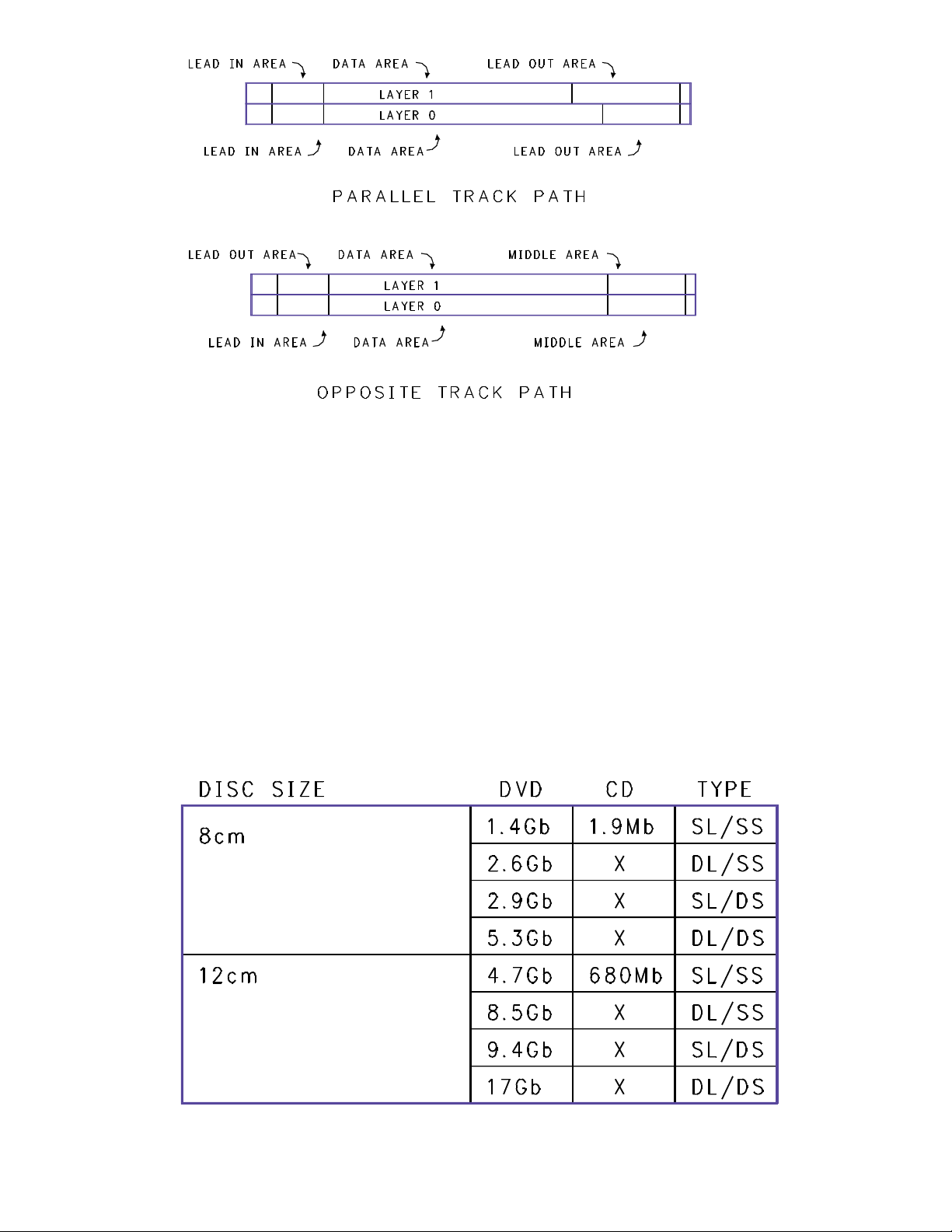
inner portion of the disc. There is a Middle Track
Area on both of the layers located on the outer
portion of the layers. The Middle Track Area links
the data on the two layers together. The Lead
Out Area is on the second layer on the inner portion of the disc.
Capacity
Because a stamped DVD can be Dual Layered
and Double Sided, there are four different capacities. Refer to Figure 13. These capacities strict-
ly pertain to raw data. The time available for
Video and Audio has many extra factors that
determine the length of time on each side or
layer. The picture complexity and the amount of
movement in the picture affect compression and
time on a disc. The number of languages affect
the time on a disc. The type and quality of the
Audio has an affect on the time also. It can be
mono, stereo, or AC-3. Therefore, the media
itself determines the capacity in time on the disc.
Figure 13 – DVD Multi-Layered Capacities
8
Figure 12 – PTP and OTP Layout

Description
The VN02 products have this feature. The End
User/Dealer Self Diagnostics work without the
need for other equipment. A number of hardware
tests are automatically executed to check for
faults in the recorder. The final test, number one,
routes video to the Composite Out jack. The signal is a Pal Color bar signal. Most televisions will
show the bars in B+W. This is dependent on the
pull in range of the monitor, as the frequencies
are shifted as compared to NTSC. The diagnosis
ends with a “FAIL” or “PASS” message.
If the message “FAIL” appears on the display, an
Error Code is displayed. If the message “PASS”
appears, the tests have been executed successfully. There can still be a failure in the recorder.
The tests do not cover the complete unit. The
following list describes the tests being performed
while the test number is being displayed on the
Front Panel.
To place the unit in the Self Test Mode, hold the
Play pushbutton on the Front Panel while suppling AC power to the unit. The word BUSY
appears on the display followed by test number.
The display counts down numerically to test if it
is performing.
The following is a list of the tests.
“Test Number” is displayed on the Front Panel
“Name” of the test
Description of the test
22
SdramWrR
Checks all memory locations of the 4Mbyte
SDRAM
21
HostdDramWrR
Checks all the DRAM connected to the microcomputer on the Digital Board
20
HostdI2cNvram
Checks the data line (SDA) and the clock line
(SCL) of the I2C bus between the host decoder
and NVRAM
19
SAA7118I2c
Checks the interface between the Host I2C controller and the SAA7118 Video Input Processor
18
VideoEncI2c
Checks the interface between the host I2C controller and Empress
17
AudioEncI2c
Checks the I2C connection between the host
decoder and Empress
16
AudioEncAccess
Tests the HIO8 interface lines between the host
decoder and the audio encoder
15
AudioEncSramAccess
Checks the access of the SRAM by the audio
encoder (address and data lines).
14
AudioEncSramWrR
Tests the SRAM connected to the audio encoder
13
AudioEncInterrupt
Tests the interrupt line between the host decoder
and the audio encoder
12
VsmAccess
Checks whether the VSM interrupt controllers
and DRAM are accessible
11
VsmInterrupt
Checks both interrupt lines between the VSM
and the host decoder
9
User Self Diagnostics (VN02)

10
VsmSdramWrR
Tests the entire SDRAM of the VSM
9
Clock11.289MHz
Switches the A_CLK of the micro clock to
11.2896 MHz
8
Clock12.288MHz
Switches the A_CLK of the micro clock to 12.288
MHz
7
BeS2Bengine
Checks the S2B interface with the Basic Engine
by sending an echo command
6
DisplayEcho
Checks the interface between the host processor
and the slave processor on the display board
5
AnalogEcho
Checks the interface between the host processor
and the microprocessor on the Analog Board
4
AnalogNvram
Checks the NVRAM on the Analog Board
3
Tuner
Checks whether the Tuner on the Analog Board
is accessible
2
LoopAudioUserDealer
Tests the components in the audio signal path:
The host decoder on the Analog Board, the
audio encoder, the VSM. The Audio is internally
looped back thru the Digital Board
1
LoopVideoUserDealer
Tests the components on the Video signal system path: - The VIP- The Video encoder- The
VSM- The host decoder. The Analog Board On
Video signal is internally routed back to the
Digital Board.
10
The User Self diagnostics in the VN04 product
are very different than the VN02 product. It has a
different Digital Board.
Press Play and apply AC power. The display will
flash quickly through a more technical display of
the Nucleus (test) it is performing. If an error is
found, the Nucleus Code and an Error Code will
be displayed. Use the Service Manual to look up
the code.
User Self Diagnostics (VN04)

11
Description
The VN02 products have this feature. The
Manual Diagnostics provide the opportunity to
perform tests and exercise the unit in a way that
helps determine which of the DVD recorder’s circuit boards are faulty. If no Errors are found, it
performs an endurance loop test.
To successfully perform the tests, the DVD
recorder must be connected to a monitor via the
video out. The Servicer must respond to what is
seen and heard on the monitor. (i.e. to approve a
test picture or a test sound). Some tests require
that a DVD+RW disc be inserted.
Structure of the Player Script
The player script (Manual Diagnostics) tests the
circuit boards in the DVD recorder: the Display
PCB, the Digital PCB, the Analog In/Out PCB
and the Basic Engine.
The Player tests are done in two phases, interactive tests and a burn in test. The interactive
tests depend strongly on user interaction and
input to determine the results and to progress
through the full test. The Burn-in Loop test will
perform the same set of tests as the dealer test,
but it will loop through the list indefinitely. Is is
especially useful if you reset the Error Log. You
can do this using ComPair. You can then read
the error codes using ComPair.
Step by Step Description
1
Press OPEN/CLOSE and PLAY buttons at the
same time and provide AC to the recorder to
start the player script. Press Play to perform the
test described on the display. Press Stop to skip
the test and go to the next test. Press Record to
indicate to the Microcomputer the desired result
malfunctioned.
2
The display shows FP SEGM. Press PLAY to
start the test. First the starburst pattern is lit.
Press Play each time to advance. Then the horizontal segments are lit, followed by the vertical
segments and the last test lights all the segments. After each of the four tests, the user has
to confirm that the correct pattern was lit.
Pressing PLAY confirms the correct pattern was
lit. Pressing RECORD indicates that the correct
pattern was not successfully lit. Press STOP to
skip this or any test.
3
The display shows FPLABELS. Press PLAY to
advance. All labels should be lit.
4
The display shows FPLIGHT ALL. Press PLAY
to advance. Everything should be lit.
5
The display shows FP LED. Press PLAY to
advance. The red Record light comes on. Press
PLAY to confirm it lit. Press STOP to skip this
test.
6
The display shows FP KEYBRD. All keys have
to be pressed to get a positive result! This
includes the Power button. Press PLAY for more
than two seconds to confirm that all the keys
were pressed and that it was shown on the display. Press STOP for more than one second to
skip this test.
7
The display shows FP REMCTL. Press PLAY to
confirm that a key on the remote control was
pressed and shown on the local display. Only
one key has to be pressed to get a successful
result.
Manual Diagnostics VN02

8
The display shows FPDIMMER. Press PLAY to
activate the dimming feature. Press Play to confirm that the text on the local display was
dimmed.
9
The display shows ROUTE VID. Press PLAY to
advance.
10
The display shows ROUTE AUD. Press PLAY to
advance.
11
The display shows COLORBAR ON.Press PLAY
to advance. An NTSC Colorbar Pattern should
appear at the output. Press PLAY to advance.
12
The display shows PINKNOISE ON. The monitor
should produce Pink noise.
13
The display shows PINKNOISE OFF. Press
PLAY to advance.
14
The display shows BE RESET. Press PLAY to
Reset the Basic Engine (Mechanism/Servo
PCB).
15
The display shows BE TRAY OPEN. Press
PLAY to open the tray. Place a RW disc in the
tray.
16
The display shows BE TRAY CLOS. Press
PLAY to close the tray.
17
The display shows BE WRITE READ. This
requires a RW disc to be in the machine. The BE
resets and a small write is preformed, and then a
read. This will take 20 seconds or so.
18
The display shows BE TRAY OPEN. This opens
the tray.
19
The display shows BE TRAY CLOS. This closes
the tray.
20
The display shows ERRORLOG READ. If there
was an error, a code will be displayed. If you
press PLAY, the diagnostic script will start an
endless loop. If the unit fails a test, the local display will display FAIL and the error code.
In case of a failure, the display shows “ FAIL
XXXXXX “The description of the shown error
code should be found in the list in the Service
Manual. Once an error occurs, press the STOP
key to jump over the failure and to continue the
diagnostics.
There is a Error Code Table in Force Manual
2064.
VN04 product does not have
Manual Diagnostics.
If you try to place the unit in diagnostic mode in
the same manner as the VN02 product, there is
no display and the unit is locked.
12

Overall Block
Key Components
The unit is made up of: the Power Supply/Analog
Board, the Front Panel, the Basic Engine, the
Digital Board, and the Digital Video Input/Output
Board. Refer to Figure 14. The DVIO board’s
circuitry is contained on the Digital Board of the
VN04 product.
Block Diagram Descriptions
Power Supply
The Power Supply is a SMPS using Hot Ground
on the primary side of the transformer. There is
no MAINS power switch. It is operating when AC
is applied. It supplies power to: the Analog
Board, the Digital Board, the Basic Engine, and
the Front Panel..
Front Panel Display
This module contains a microcomputer that doubles as a fluorescent display driver. It receives
the IR inputs and the keyboard inputs. It communicates the user input from the Keyboard and IR
Receiver via the I2C Bus to the Microcomputer
on the Analog Board.
Basic Engine (BE)
This consists of the Mechanism and Servo control PCB. The Mechanism is essentially the same
as a DVD with the exception of the Optical
Pickup Unit, OPU. The OPU has a dual direction
signal and light path, one for the write signal and
one for the play signal. The OPU has three ICs
mounted on it for processing laser signals.
These include: the Laser Drive IC or LADIC, the
Dvd Recordable Optical Preprocessor IC or
DROPPI, and the Non-Volatile RAM or NVRAM
to store its electro-mechanical settings.
The Servo controls the Mechanism. It handles
the HF signal to and from the OPU. It uses a
Microcomputer to control all aspects of the Servo
operation. This includes: tray operation, spindle
speed, focus, HF preprocessing, and radial positioning of the OPU.
Digital PCB
This module performs many functions. It interfaces between the Basic Engine and the rest of
the unit. There are two Digital Boards in the
DVDR75. The Product Number is different signifying which Digital Board is in the unit. The one
described here is the VN02 product. The functionality and connections are the same. The
VN04 product contains the DVIO circuitry, and a
different chipset. A separate block diagram follows the Digital Board’s Circuit Description.
During record, it encodes analog video and digital audio into a recordable digital data stream.
The Analog to Digital Converter for video is part
of a Video Input Processor, VIP, that supplies the
MPEG2 Encoder. The VIP sends parallel digital
video to the EMPRESS and the VSM. The
Empress is the MPEG2 Encoder. It receives
video from the VIP and audio from the Analog
Board. The Audio is A/D converted on the Analog
Board. The EMPRESS is a microcomputer. It
has its own SDRAM. It supplies MPEG2 data to
the VSM, Versatile Stream Manager. Using sync
from the Digital Video coming from the VIP, the
VSM converts the signal into an I squared S serial signal. The serial data is sent to the BE to be
recorded on the disc.
During playback, the MPEG2 Decoder receives
its I squared S input directly from the BE. It
decodes the data stream into analog Video and
digital Audio. Both are sent to the Analog Board.
Digital Video is provided to the Line Doubler. The
Line Doubler receives 11 bit digital YUV. The
Line Doubler produces progressive scan digital
Y/U/V that goes to the Digital to Analog Encoder.
Y, Pr, and Pb are sent to the Analog Board.
The Host Decoder is the Master of the I squared
C bus that provides communication between the
Microcomputers: Empress, VIP and the Line
Doubler. The VSM Communicates to the System
Control Microcomputer Via UART1. UART2 provides communication between the Digital Board
and the DVIO Board. EMI uses Flash memory to
provide the Boot up sequence and the operational firmware. Updates can be loaded to
13
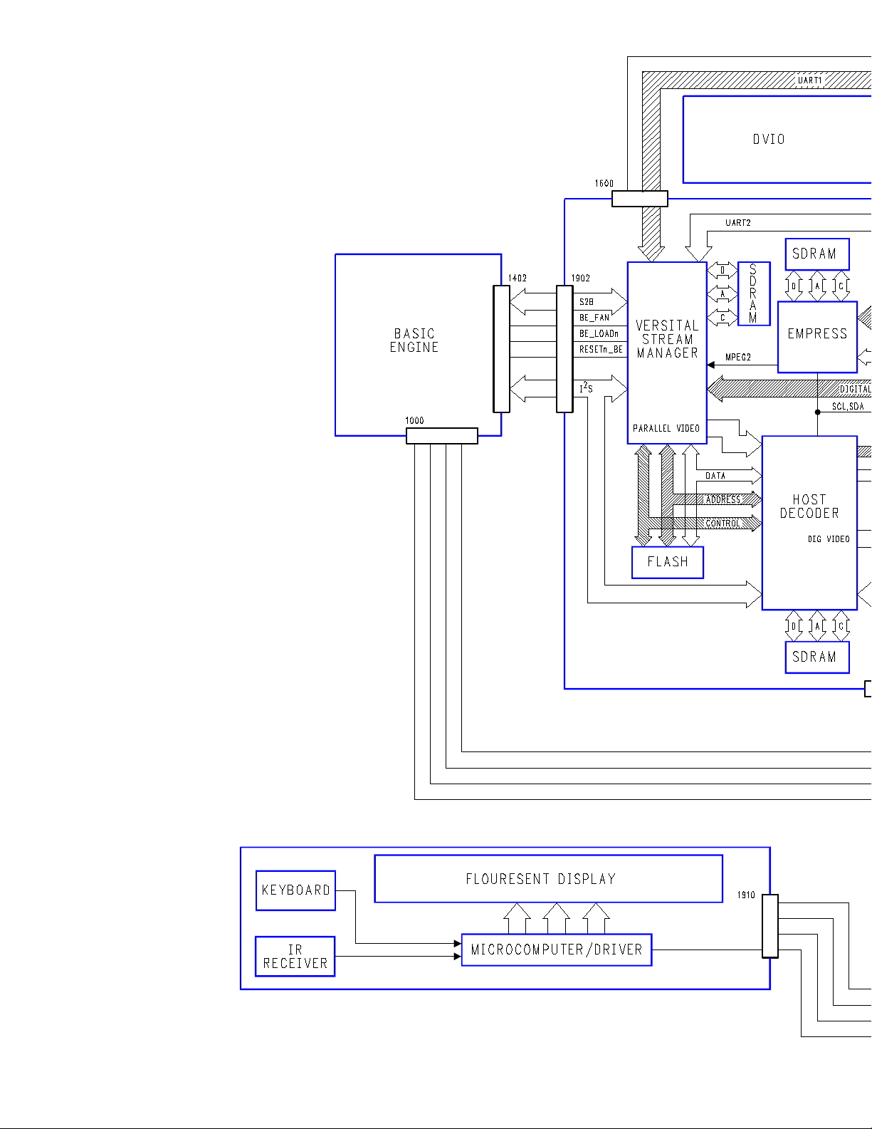
Figure 14 – O
14
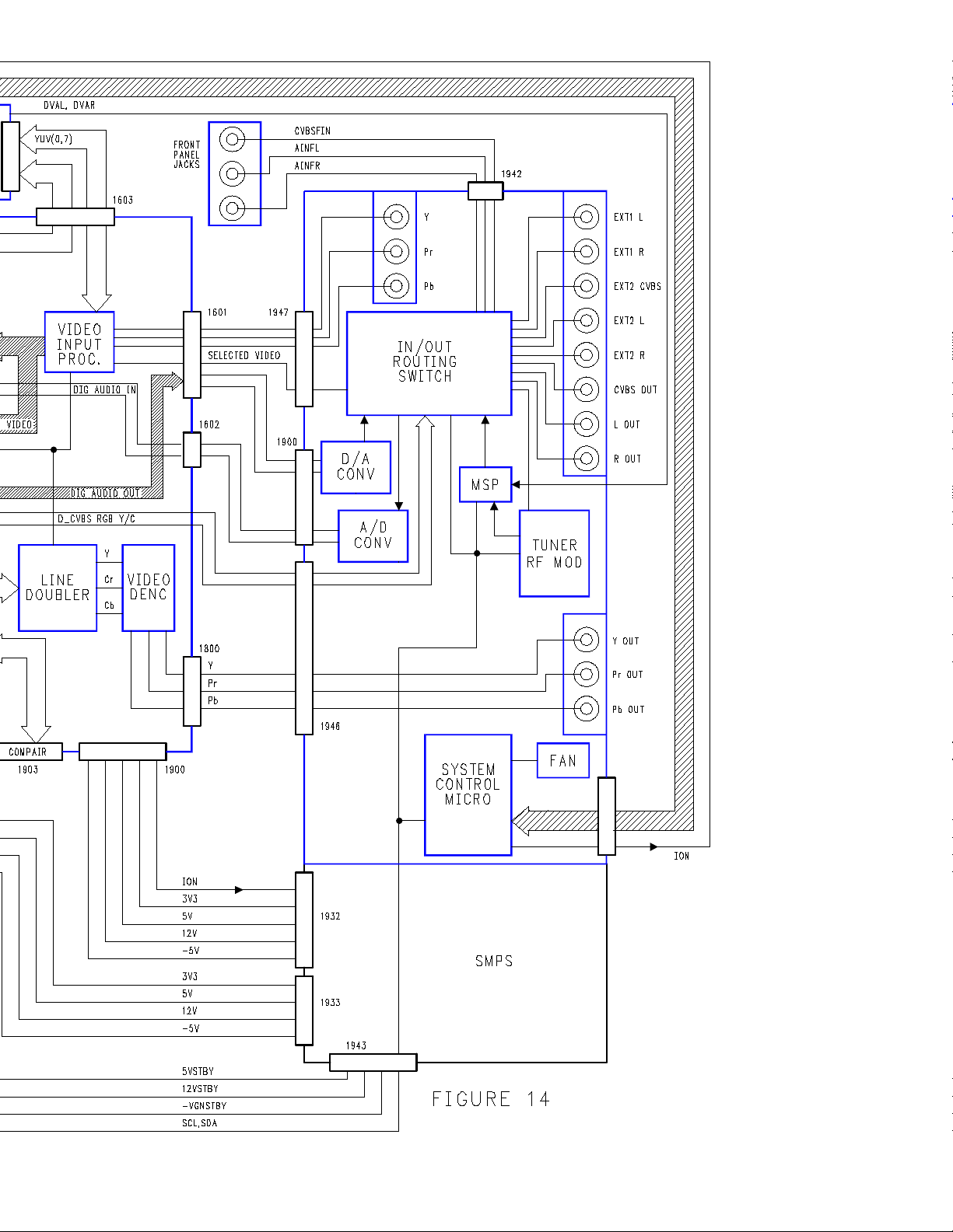

enhance operation of the unit. At present, the
update disc is version 6.1.
Analog PCB
This module contains: the Power Supply, the
System Control Microcomputer, all the A/V inputs
and outputs including a Tuner/RF Modulator.
Source selection and output type are controlled
by the microcomputer. The microcomputer controls many functions throughout the unit including: Power up, user input, input/output selection,
the Tuner, the D/A, and A/D functions of the
Audio. It also controls the Fans.
Input selection is an important function performed by the analog board. The user selects
between: External 1 and 2, DVIO, Tuner Video,
and Front Panel jacks.
Audio processing is performed on the Analog
Board. The Audio signal coming from the Tuner
has a separate demodulator. The Multi System
Processor, MSP, demodulates the audio and
sends the signal to the Routing Switch. The MSP
selects between Tuner Audio and the DVIO
Audio signals. The selected audio is sent to the
A to D Converter. Digital Audio is supplied to the
Digital Board for recording.
DVIO PCB
The Digital Video Input Module provides IEEE
1394 translation to the DVD recorder. It separates the Digital Video and Audio. The Digital
Audio is decoded and sent as Analog Audio to
the Analog Board. Digital Video (DV) is supplied
to the Video Input Processor on the Digital
Board. The DVIO board communicates with the
Digital board via UART2.
Power Supply
This unit uses a Switch Mode Power Supply,
SMPS. It operates whenever ac is applied. A
MOSFET transistor turns On and Off in an oscillator fashion, driving a transformer. The primary
half of the supply uses a Hot Ground. The primary side of the circuit provides drive and coarse
control of the power supply. The secondary side
of the circuit rectifies and filters the output of the
transformer to produce many output voltages. It
uses a cold ground, signal ground system. The
output is monitored for precise regulation. The
5Vdc is supplied to the anode of the Optic
Coupler’s diode and fed to the Shunt Regulator.
The regulation path includes an Optic Coupler to
accommodate the different grounding systems.
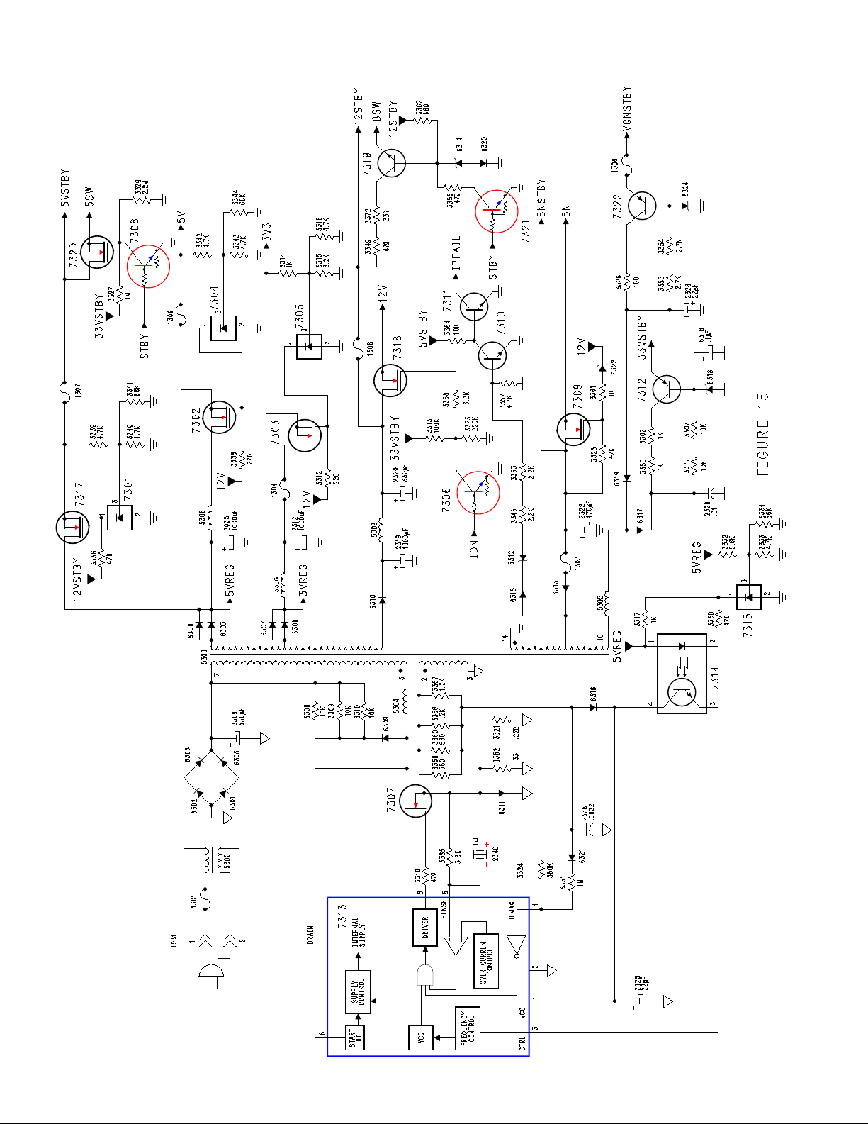
Circuit Description
AC Input Circuit
The AC input is rectified by diodes 6301, 6302,
6305, 6306, and filtered by C2309. Refer to
Figure 15. The voltage on C2309 is approximately 155V. It can vary from 150V to 160V,
depending on the AC input voltage.
Start Circuit
The start up of this power supply is mostly contained in IC7313. The Drain supply voltage goes
to Pin 8 of the IC. The running supply for the IC
is Pin 1 of the IC. The Supply Control provides a
measured supply to the VCO and the Driver for
start up. The power supplied is not enough to
keep the unit operating. If the supply does not
operate and supply Pin 1 with operating power,
the unit stalls.
When the power plug is connected to AC, the
MOSFET 7307 will start conducting when the
gate voltage reaches the threshold value. A current starts to flow in the primary winding of 5300,
Pins 7 and 5. While the MOSFET is conducting,
energy is building up in the transformer. The current flow through the MOSFET is sensed by
R3352, and 3321. When the current level rises
high enough to provide a voltage drop on these
components, 7307 is turned Off by the driver circuit. Diode 6311 protects the control circuit in

case of failure of the MOSFET by providing an
upper-limit to the voltage that can remain on the
source of the MOSFET.
Coarse Regulation
The positive portion of the signal on Pins 2 and 3
will be rectified via D6316, charging C2325. In
time, the voltage on C2340 will reach 9 to
13Vdc. This value depends on the value of the
Mains voltage and the load. This is also used as
a regulation supply for the optic coupler IC7314.
The control circuit consists of a VCO, the Driver,
an Op Amp and Gate that are fed by the sensing
resistors, 3352 and 3321, and C2340. This circuit controls the conduction time and the switching frequency of the MOSFET. It switches Off the
MOSFET as soon as the voltage on the source
of 7307 reaches a certain value.
Demagnetization or complete magnetic field collapse is desired before the next drive signal is
applied to the MOSFET. This improves efficiency
by reducing the power necessary to build a magnetic field in the transformer. Pin 4 is the Demag
input. When Pin 4 is near 0Vdc, the gate is
enabled, allowing the next oscillation to occur.
Secondary Rectifier/Smoothing Circuit
There are six Rectifier/Smoothing circuits on the
secondary side. Each supply voltage depends on
the number of windings in the transformer. From
these circuits, several voltages are derived.
Precise Regulation
The 5VREG is monitored for regulation. The regulation circuit consists of an Optic-Coupler, 7314,
a shunt regulator, 7315, and a voltage divider
network. The Optic-Coupler isolates the Hot
Ground on Pin 2 of 7313 from the Cold Ground
voltage on 7315. 7315, a Shunt Regulator, has
two component characteristics. It is a very stable
and accurate reference diode and a high gain
amplifier.
7315 will conduct from cathode to anode when
the 5VREG is rises higher than the 5Vdc. The
5VREG is divided down to a 2.5V reference voltage. If the 5VREG and subsequently the reference voltage is lower, the cathode current is
almost zero. The cathode current flows through
the LED of the Optic-Coupler, controlling the current through the transistor portion of the OpticCoupler. The collector current of 7314 will adjust
the feedback level of the error voltage at Pin 3 of
7313.
There are standby and switched supplies. The
5VSTBY, 12VSTBY, 5NSTBY, 33VSTBY and the
VGNSTBY supplies are always present when AC
is supplied. The VGNSTBY supply ia a -33Vdc
dedicated to the Front Panel Fluorescent Tube
as a grid supply. The 5SW, 8SW, 12V, 5V, and
3V3 supplies are switched.
The STBY control voltage switches On the 5SW
and the 8SW. As part of the first layer of Power
Up, the System Control Microcomputer pulls the
STBY line Low. This removes bias to 7308 and
7321. This allows the standby supplies to bias
7319 and 7320 On. These supplies go to the RF
Unit, the Sound IF and the Input Matrix.
The ION control voltage turns the unit On and
Off. When the user turns the power On, the ION
control voltage goes Low, turning 7306 Off. The
33VSTBY supply is allowed to turn On 7318.
The switched 12V becomes available. The
Switched 12V switches On the 3V3 and the
switched 5V supplies. The 3V3 and 5V supplies
are regulated by shunt regulators, controlling
MOSFETs.
Overcurrent Protection Circuit
When the output is shorted, the current through
the FET will produce a large voltage drop across
the source resistors of the FET. When Pin 5 is
elevated, the Op amp’s output is low, disabling
the output of the Driver. This switches Off the
drain current of the MOSFET, 7307. The start circuit will try to start up the power supply again. If
the short still exists, the complete start and stop
sequence will repeat. The power supply is in a
hiccup mode and is ticking.
Overvoltage Protection Circuit
If the regulation circuit does not function due to
an error in the control loop, the regulated output
voltage will increase. This overvoltage is sensed
15
16
Figure 15 - Power Supply Circuit

on the hot ground side of the transformer at Pins
2 and 3. When an overvoltage is detected, the
Demag circuit will activate the inverter. The
power supply will be shutdown until the voltage
returns to zero. it will then try to restart.
The IPFAIL signal is used as a Power Fail measurement signal. During normal operation, 7310
is biased On by 6315 and 6312. When power is
interrupted that Bias is removed prior to the Filter
capacitors draining off their charge. 7310 turns
Off, allowing the 5VSTBY to turn On 7311. The
IPFAIL goes low. This signal goes to the System
Control Microcomputer and Mute circuits.
Microcomputer
The Microcomputer, IC7804, is a 16-bit processor
with internal ROM and 4kB RAM. It uses External
RAM, IC 7803, and Flash, IC 7805. It is mounted
on a Sub Board soldered into the Analog Board.
Refer to Figure 16. The System Clock operates at
24MHz. It uses an I2C interface to communicate
with the other Microcomputers in the unit. The
clock rate is approximately 95kHz. The Reset Pin
is high during normal operation. The microcomputer uses non-volatile EEPROM, 7805. The
EEPROM stores data specific to the device, such
as the AFC-reference value, clock-correction-factor, etc.
Power up
7804 controls power up of the unit. There are
three layers to the power up sequence. The first
layer involves the Analog Board and the Front
Panel. The second layer involves the Digital
Board and the BE. The third involves the Front
Panel and the Analog Board.
The first layer controls the first set of switched
supplies. After the System Control Microcomputer receives its reset, the STBY control
voltage goes Low to turn On the first set of
switched supplies, the 5SW and the 8SW. It
communicates on the I2C bus initializing the RF
Unit, the Sound IF, and the Input Matrix ICs. If
they respond properly, it then communicates on
the I2C to the Front Panel Microcomputer. If the
Front Panel Microcomputer responds properly,
the ION control voltage goes Low.
The second layer occurs when the ION switching
voltage goes Low. It comes from the System
Control Microcomputer. The ION control voltage
passes through the Digital Board to the Power
Supply and turns On a second set of switched
voltages. These include the 3.3Vdc supply. The
3.3Vdc supply is the main B+ to many of the
microcomputers throughout the unit. The System
Control Microcomputer then sends out the
IReset signal to 7902 on the Digital Board. This
IC produces a delayed Resetn signal line for
7200. 7200 activates its I2C and provides several reset and initialization signals for the Digital
Board, DVIO, and the BE. They all go through a
self test. If the self test succeeds, the VSM communicates through UART1 that the system is operating, and the unit can enable the Front Panel
to accept a response. The Front Panel Microcomputer then places four dashes on the Front
Panel Display. ION goes High placing the unit in
Standby, waiting for keyboard input. This normally takes 6-8 seconds. The System Control Microcomputer allows 10 seconds for the UART1
response. If it does not come, the unit goes into
sleep mode, and will not accept keyboard input.
When the Front Panel Microcomputer receives a
keyboard response, it communicates that action
to the System Control Microcomputer to switch
back On the second layer of switched voltages.
The System Control Microcomputer controls the
operation of the entire unit. It uses UART1 for
communication with the Microcomputers on the
Digital Board. It uses the I squared C Bus ,I2C to
communicate with devices on the Analog Board.
It receives composite sync from the Selected
video source. This is to determine that a good
signal source has been selected before the unit
is allowed to record.
17
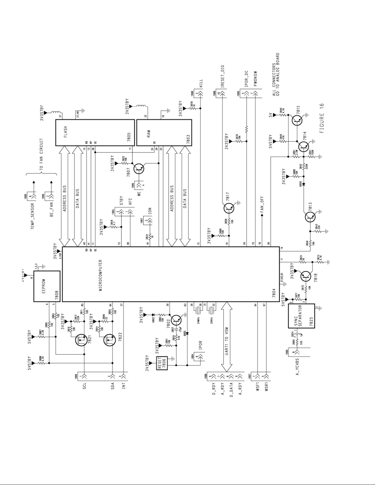
Figure 16 - System Control Microcomputer
18

Front Panel
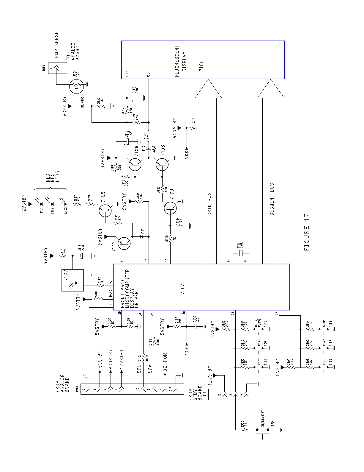
The main elements of the Front Panel are the
microcomputer, 7103, the Display Tube, and the
keyboard. Refer to Figure 17. 7103 is an 8-bit
microcomputer fitted with 96kB ROM and 3kB
RAM and is responsible for the following functions:
Fluorescent Display driver
Monitoring the keyboard matrix
Communicating with the System Control
Microcomputer
Decoding the remote control commands
from the infrared receiver, 7107.
Activation of the display
The Fluorescent Tube operates using a grid and
segment scanning matrix. AC is supplied by a
switching regulator consisting of 7106, 7108, and
7109. A squarewave is produced by the
Microcomputer on Pin 19. The Signal is amplified
by 7109 and supplied to the Push/Pull output
Amp.The signal passes through 5104 going to
the tube. With AC supplied, the microcomputer
scans the elements in the tube to determine
what segments light up. The system clock is
generated with the 8MHz crystal, 1100.
Keyboard Matrix
There are 6 keys on the display board and 1 on
the Standby board. A resistor network is used to
generate a specific voltage value, depending on
the key pressed, via the resistors 3300, 3103,
3104, 3106, 3108, 3110, and, 3130. This RTL
data (voltage Level) is sent to 7103 on Pins 36
and 37. Pressing keys simultaneously may lead
to undesired functions.
Communication with the System Control
Microcomputer occurs on a I Squared C bus,
SDA and SCL. The Front Panel receives standby
supplies, so it is always live when AC is suppled
to the set. The System Control Microcomputer
Hosts the I squared C Bus. The System Control
resets and initiates the I squared C bus. The
Front Panel Microcomputer resets simultaneously and communicates to the System Control
Microcomputer that It is operating. The push buttons and IR receiver are then monitored.
IR Receiver
The IR receiver, 7107, contains a bandpass
amplifier as well as a photo-diode. The photodiode receives approximately 940nm infrared
pulses. The pulses are amplified and demodulated. On the output of the IR receiver, 7107, is a
pulse sequence at TTL levels. The IR signal
appears on Pin 20 of 7103.
The Front Panel contains a Thermal Sensor. It is
a temperature coefficient resistor. As the temperature rises, so does the resistance. This voltage
is sent to the Fan Control Circuit.
The Record LEDs are controlled by the Front
Panel Microcomputer. 7105 and 7112 are the
LED drivers. Pin 3 of the microcomputer goes
low to turn on the lights. That turns On 7112
which in turn turns On 7105. 7105 pulls current
through the diodes illuminating them.
19
20
Figure 17 - Front Panel Circuit

Analog Processor Board
The Analog Board controls all analog input/output selection, and routing. It houses the System
Control Microcomputer. The System Control
Microcomputer controls the routing and other
functions on the board. One of its other main
functions is to control power and initialization of
the unit. It implements Keyboard instructions.
The board has the Optical Audio Out and the
Coax Digital Audio Output circuits. It controls the
Tuner. The Audio D/A and A/D conversion is performed on this Board. It contains the Fan Control
circuit and houses the first Reset circuit for the
System Control Microcomputer.
There are three circuits that can Mute the audio.
The Digital Board produces the D_KILL signal.
There is a power fail circuit, which is necessary
to mute AUDIO when power is lost, IPFAIL. The
System Control Microcomputer produces the Kill
signal.
Tuner/RF Unit
The Tuner is part of and RF Unit. It contains the
Tuner, An RF Modulator and the Demodulator/IF.
The Tuner is capable of receiving 125 channels,
and is cable ready. Refer to Figure 18. The RF
connections on the back are part of the Tuner,
RF Modulator. The RF Unit receives two supply
voltages, 33Vdc and SW5Vdc. The channel
selection information is communicated via the
I2C lines. The output channel is selected by
CSW_SSW control voltage. Video is output from
Pin 24. 7700 buffers the signal before it goes to
Input Matrix. The RF Unit does not perform
audio demodulation. The audio signal leaves the
RF Unit as Sound IF, from Pin 15 of the RF Unit.
The Digital Board’s output video, D_CVBS goes
to the RF Unit for the RF Modulator to output the
signal on channel 3 or 4. The audio signal
returns to the RF Unit on Pin 2 to be used by the
RF Modulator. The AFT signal comes from the
Microcomputer.
Audio Demodulator
The Sound Processor, 7600, demodulates the
Audio. MPS means Multi System Processor. The
I2C bus controls its operation. It uses two power
supplies, the 5Vdc and the 8V Switched. IC 7600
has its own oscillator on Pins 5 and 6. Amplitude
and bandwidth of the demodulated audio signals
can be determined in 7600 using the I2C bus. It
sends analog audio back to the RF Unit from Pin
26. The audio coming from the Digital Board,
ARDAC and ALDAC, go into the Sound IF. The
I2C bus controls what Audio is output, the Tuner
Audio, or the Digital Board’s output. The Audio
signal output from the MSP is available at Pins
30, AFER, and 31, AFEL. 7600 controls the
audio input selection via RAS1 and RAS2
switching voltages. They go to the Input
Selection Switch, 7501.
7419 and 7420 perform level matching between
the 5V serial clock and data lines of the Tuner
and Demodulator to the 3.3V levels coming from
the Microcomputer.
Input Matrix
The A/V I/O switching is controlled by a switch-
ing matrix, 7408. It is controlled via the I2C Bus.
The Matrix controls what source will be supplied
to the Digital Board. There are several choices:
Tuner Video, External 1(Y/Pr,Pb), External 2
Video, and Front Video. In addition there are 2
Y/C inputs. All switches have 6 dB amplification
on the outputs. The Matrix is not responsible for
handling the Y/Pr,Pb. It goes directly to the
Digital Board when present.
The user selects what source is to sent to the
Digital Board on Pin 9 of 1947. The I2C Bus
communicates this data to the Matrix IC. The
selected source comes out Pin 21 of 7408. The
Matrix communicates channel selection control
for the RF Unit on Pin 44.
The unit can receive a 16 by 9 input using the
Y/C inputs. The Microcomputer must detect this
format and communicate it to the Digital Board.
21
 Loading...