

Page 1
Safety Information, General Notes & Lead Free Requirements
2. Safety Information, General Notes & Lead Free Requirements
2.1 Safety Instructions
2.1.1 General Safety
Safety regulations require that during a repair:
• Connect the unit to the mains via an isolation transformer.
• Replace safety components, indicated by the symbol
only by components identical to the original ones. Any
other component substitution (other than original type)
may increase risk of fi re or electrical shock hazard.
Safety regulations require that after a repair, you must return
the unit in its original condition. Pay, in particular, attention to
the following points:
• Route the wires/cables correctly, and fi x them with the
mounted cable clamps.
• Check the insulation of the mains lead for external
damage.
• Check the electrical DC resistance between the mains
plug and the secondary side:
1. Unplug the mains cord, and connect a wire between
the two pins of the mains plug.
2. Set the mains switch to the ‘on’ position (keep the
mains cord unplugged!).
3. Measure the resistance value between the mains
plug and the front panel, controls, and chassis
bottom.
4. Repair or correct unit when the resistance
measurement is less than 1 MΩ.
5. Verify this, before you return the unit to the customer/
user (ref. UL-standard no. 1492).
6. Switch the unit ‘off’, and remove the wire between the
two pins of the mains plug.
2.1.2 Laser Safety
This unit employs a laser. Only qualifi ed service personnel
may remove the cover, or attempt to service this device (due
to possible eye injury).
,
2.2 Warnings
2.2.1 General
• All ICs and many other semiconductors are susceptible to
electrostatic discharges (ESD,
during repair can reduce life drastically. Make sure that,
during repair, you are at the same potential as the mass
of the set by a wristband with resistance. Keep
components and tools at this same potential.
Available ESD protection equipment:
– Complete kit ESD3 (small tablemat, wristband,
connection box, extension cable and earth cable)
4822 310 10671.
– Wristband tester 4822 344 13999.
• Be careful during measurements in the live voltage
section. The primary side of the power supply, including
the heatsink, carries live mains voltage when you
connect the player to the mains (even when the
player is ‘off’!). It is possible to touch copper tracks and/
or components in this unshielded primary area, when
you service the player. Service personnel must take
precautions to prevent touching this area or components
in this area. A ‘lightning stroke’ and a stripe-marked
printing on the printed wiring board, indicate the primary
side of the power supply.
• Never replace modules, or components, while the unit is
‘on’.
2.2.2 Laser
• The use of optical instruments with this product, will
increase eye hazard.
• Only qualifi ed service personnel may remove the cover or
attempt to service this device, due to possible eye injury.
• Repair handling should take place as much as possible
with a disc loaded inside the player.
• Text below is placed inside the unit, on the laser cover
shield:
). Careless handling
Laser Device Unit
Type : Semiconductor laser
GaAlAs
Wavelength : 650 nm (DVD)
: 780 nm (VCD/CD)
Output Power : 20 mW
(DVD+RW writing)
: 0.8 mW
(DVD reading)
: 0.3 mW
(VCD/CD reading)
Beam divergence : 60 degree
CLASS 1
LASER PRODUCT
Figure 2-1
Note: Use of controls or adjustments or performance of
procedure other than those specifi ed herein, may result in
hazardous radiation exposure. Avoid direct exposure to beam.
CAUTION VISIBLE AND INVISIBLE LASER RADIATION WHEN OPEN AVOID EXPOSURE TO BEAM
ADVARSEL SYNLIG OG USYNLIG LASERSTRÅLING VED ÅBNING UNDGÅ UDSÆTTELSE FOR STRÅLING
ADVARSEL SYNLIG OG USYNLIG LASERSTRÅLING NÅR DEKSEL ÅPNES UNNGÅ EKSPONERING FOR STRÅLEN
VARNING SYNLIG OCH OSYNLIG LASERSTRÅLNING NÄR DENNA DEL ÄR ÖPPNAD BETRAKTA EJ STRÅLEN
VARO! AVATTAESSA OLET ALTTIINA NÄKYVÄLLE JA NÄKYMÄTTÖMÄLLE LASER SÄTEILYLLE. ÄLÄ KATSO SÄTEESEEN
VORSICHT SICHTBARE UND UNSICHTBARE LASERSTRAHLUNG WENN ABDECKUNG GEÖFFNET NICHT DEM STRAHL AUSSETSEN
DANGER VISIBLE AND INVISIBLE LASER RADIATION WHEN OPEN AVOID DIRECT EXPOSURE TO BEAM
ATTENTION RAYONNEMENT LASER VISIBLE ET INVISIBLE EN CAS D’OUVERTURE EXPOSITION DANGEREUSE AU FAISCEAU
Figure 2-2
Page 2
Safety Information, General Notes & Lead Free Requirements
2.3 Lead Free Requirement
Information about Lead-free produced sets
Philips CE is starting production of lead-free sets from
1.1.2005 onwards.
INDENTIFICATION:
Regardless of special logo (not always indicated)
One must treat all sets from 1 Jan 2005 onwards, according
next rules.
Example S/N:
Bottom line of typeplate gives a 14-digit S/N. Digit 5&6 is the year, digit 7&8 is
the week number, so in this case 1991 wk 18
So from 0501 onwards = from 1 Jan 2005 onwards
• Special information for BGA-ICs:
- always use the 12nc-recognizable soldering temperature
profi le of the specifi c BGA (for de-soldering always use the
lead-free temperature profi le, in case of doubt)
- lead free BGA-ICs will be delivered in so-called ‘drypackaging’ (sealed pack including a silica gel pack) to
protect the IC against moisture. After opening, dependent
of MSL-level seen on indicator-label in the bag, the
BGA-IC possibly still has to be baked dry. (MSL=Moisture
Sensitivity Level). This will be communicated via AYSwebsite.
Do not re-use BGAs at all.
• For sets produced before 1.1.2005 (except products of
2004), containing leaded solder-alloy and components,
all needed spare-parts will be available till the end of the
service-period. For repair of such sets nothing changes.
• On our website www.atyourservice.ce.Philips.com you
fi nd more information to:
BGA-de-/soldering (+ baking instructions)
Heating-profi les of BGAs and other ICs used in Philips-sets
You will fi nd this and more technical information within the
“magazine”, chapter “workshop news”.
For additional questions please contact your local repair-helpdesk.
Important note: In fact also products of year 2004 must be treated in this way as long as you
avoid mixing solder-alloys (leaded/ lead-free). So best to always use SAC305 and the higher
temperatures belong to this.
Due to lead-free technology some rules have to be respected by the
workshop during a repair:
• Use only lead-free solder alloy Philips SAC305 with order
code 0622 149 00106. If lead-free solder-pate is required,
please contact the manufacturer of your solder-equipment.
In general use of solder-paste within workshops should be
avoided because paste is not easy to store and to handle.
• Use only adequate solder tools applicable for lead-free
solder alloy. The solder tool must be able
o To reach at least a solder-temperature of 400°C,
o To stabilize the adjusted temperature at the solder-tip
o To exchange solder-tips for different applications.
• Adjust your solder tool so that a temperature around 360°C
– 380°C is reached and stabilized at the solder joint.
Heating-time of the solder-joint should not exceed ~ 4 sec.
Avoid temperatures above 400°C otherwise wear-out of
tips will rise drastically and fl ux-fl uid will be destroyed. To
avoid wear-out of tips switch off un-used equipment, or
reduce heat.
• Mix of lead-free solder alloy / parts with leaded solder alloy
/ parts is possible but PHILIPS recommends strongly to
avoid mixed solder alloy types (leaded and lead-free).
If one cannot avoid or does not know whether product is
lead-free, clean carefully the solder-joint from old solder
alloy and re-solder with new solder alloy (SAC305).
• Use only original spare-parts listed in the Service-Manuals.
Not listed standard-material (commodities) has to be
purchased at external companies.
Page 3

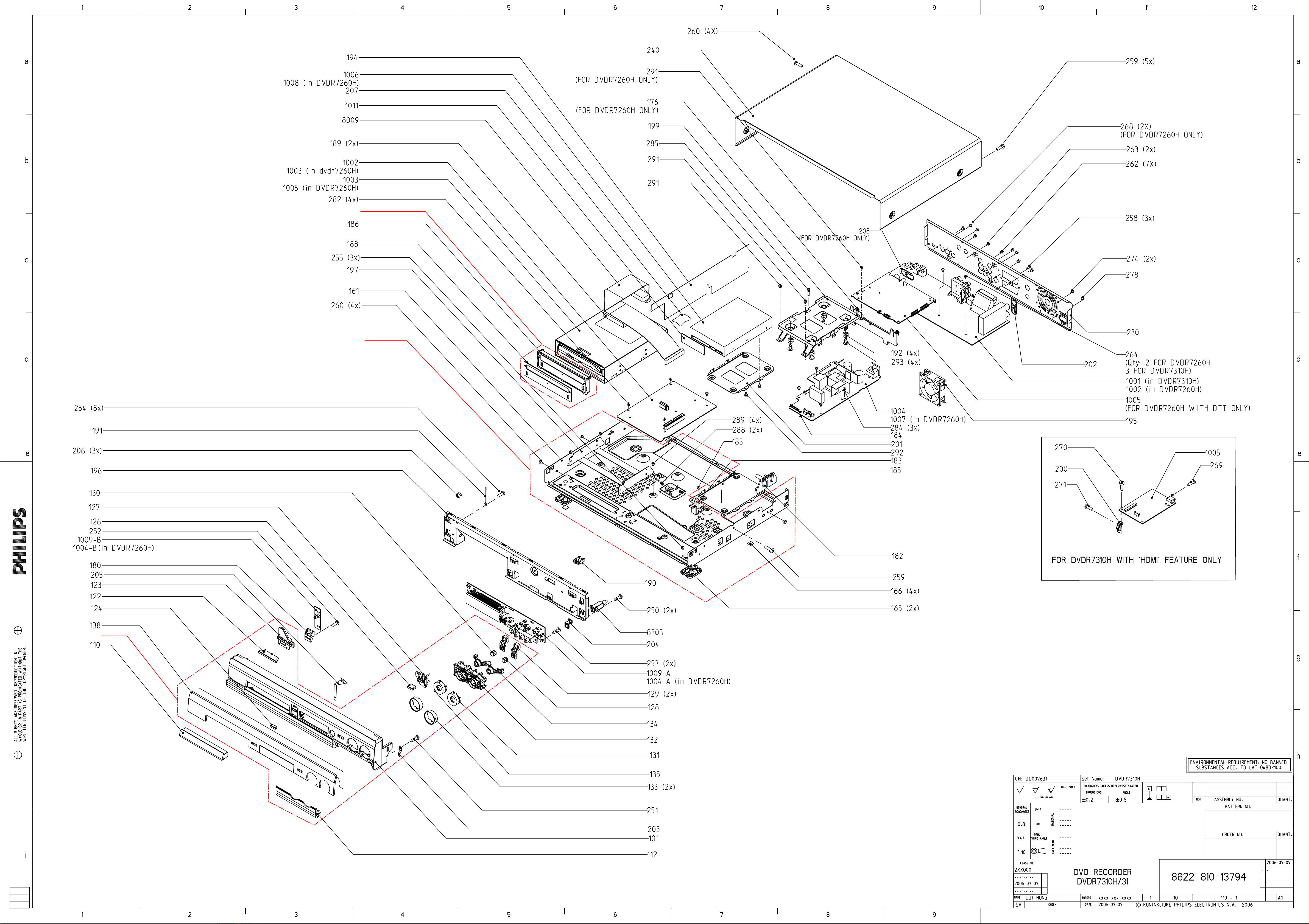
DVDR7260H/05/31/58 Service Part List
0110 3139 244 15191 COVER TRAY DVDR7260H
0182 3103 604 00291 SCREW SAFETY HOLDER
0189 3103 603 20141 SPACER RUBBER IDE CABLE
0190 2422 015 00493 SADDLE WIRE NY6/6 NT 19.1MM B
0192 3103 604 01861 DAMPER HDD
0194 3103 603 20201 AIR GUIDE
0195 2822 031 00041 FAN 12VDC 0.8W 3100RPM B
0197 3139 241 21371 BRACKET LOADER
0200 3103 604 01451 BRACKET DTTM
0202 3103 601 20612 SPRING GROUND TUNER
0204 3103 601 20212 SPRING I-LINK
0205 3103 601 20291 SPRING ESD
0206 3103 601 20231 SPRING GROUND
0208 3103 601 20612 SPRING GROUND TUNER
0230 3139 247 61331 PLATE BACK DVDR7250H/05
0240 3103 607 51621 COVER ASSY DVDR5300H
0292 2522 200 98475 SCR PAN TORX ST BK #6-32X6
0293 3103 600 30021 SCREW-DAMPER-M3
0341 2422 549 00923 REMOTE CONTR DVDR7250H B
0345 2422 070 98135 $ MAINSCORD UK 5A 1M8 VH BK B /05
0345 2422 070 98151 $ MAINSCORD EUR 1M5 BK B /31/58
0351 2422 076 00825 CBLE SCART 1M5 SCART 21P BK B
0352 2422 076 00522 G-LINK CABLE & TRANSMITTER
0353 3103 140 25022 CONNECT. CABLE PAL
0901 3143 027 66181 FRONT CAB ASSY DVDR7260H
0902 3143 027 63321 COVER DUST ASSY DVDR9000H
0920 3143 027 66201 FRAME ASSY DVDR7310H
1002 3139 248 87921 PBAS AB 04 7250H
1003 3139 248 87871 PBAS CHRYFO5-8 PANEL DVDR7250H
1004 3103 608 51242 PBAS DC 04 N1
1005 3139 247 11362 MODULE DRIVE D4.3 CLOSED
1006 3104 129 81451 PBAS DTTM DVD RW B
1007 3139 247 11985 $ MODULE PSU 05H8000 EU
1008 2822 062 00095 HDD 3.5 160GB 6L160P0 (MAXT)Y
1009 2422 549 00107 FERRITE CORE RP 25X5X12 Y
1010 3103 601 00861 FFC FOIL 40P/180/40P BD UL
8001 3103 601 00591 CBLE KR 11P/160/11P KR UL
8002 3103 601 00621 FFC FOIL 7P/290/7P BD FLD UL
8003 3139 241 02421 FFC FOIL 15P/280 AD 1MMP FOLD
8004 3103 601 00631 FFC FOIL 10P/315/10P BD FLD UL
8007 3139 241 02431 FFC FOIL 30P/220 BD 0.5MM FOLD
8008 3103 601 00442 CBLE KR 12P/130/12P UL
8009 3103 601 00611 CBLE IDE 40P/400/40P IDE UL
8010 3139 131 02551 FFC FOIL 07P/180/07P BD 1MMP
Page 4

8011 3139 241 02441 FFC FOIL 06P/140/06P AD 1MMP
8012 3103 601 00561 CBLE EHR 4P/430/4P LC UL
8013 3103 601 00751 FFC FOIL 22P/220/22P BD FLD UL
8026 3103 601 00721 FFC FOIL 22P/220/22P BD FLD UL
8030 3139 241 01991 CBLE HR 04P/120 LC EH 04P/400
8301 3103 601 00651 FFC FOIL 13P/600/13P AD UL
8302 3103 601 00311 KR 9POL GESCH 370MM
8303 3103 601 00361 IEEE 1394 CHRYSALIS 350MM
Note: $ represent Safety Part
Page 5
0902
0920
0901
8622 810 13794 dd 2006-09-14
Page 6
123456
0803 E4
1700 E1
2700 A2
2701 B3
2702 A2
2703 D3
A
1
B
A
C
B B
D
1700
TMQZ2
owner.
is prohibited without the written consent of the copyright
All rights reserved. Reproduction in whole or in parts
E
C
F
D
G
2705 E3
2707 C3
7701
BC857BW
I700
3704
100R
I701
1920
VIDOUT
RFAGC
TUNER
SIFOUT
VFV
to IOV,FOME
F705
18
AFT
GND2
VTU
NC5
MB
SDA
SCL
GND1
AOUT
NC4
NC3
NC2
NC1
BB
21
2708 C4
2709 B3
2710 C1
3706
2K2
17
16
15
14
13
12
10
11
9
8
7
6
5
4
3
2
1
2711 C1
2712 D4
3700 A2 5706 D4
3701 A2
3704 B1
3706 A1
5700 A22704 E3
5702 D3
5703 C4
23
5V
SIF1
to MSP
5700
22u
2711
2701
25V
22u
6.3V47u
F704
2710
F703
F702
2700
22n
3700
47K
3701
47K
I703
F701
2702
not used
100n
5704 C4
5705 D3
2709
I704
I706
10n
5705
10n
Bead
2703
7701 A1
F700 D1
F701 E3
5VSTBY
5VSTBY
2707
delete for DTTM
100n
F702 D3
F703 D3
F704 C3
from PS
5704
Bead
47p
not used
33VSTBY
5702
10u
F705 B1
I700 A1
I701 B1
I703 B2
I704 C3
I705 C4
I706 C3
I707 C4
A
4
5V
33VSTBY
B
5V
33VSTBY
A
C
D
E
C
F
D
G
2708
5703
Bead
47p
not used
2712
I705
I707
5706
10u
25V10u
for DTTM only
SCL_5V
from CU
SDA_5V
from/to CU
5VSTBY
-403A
E
H
I
CHN SETNAME dvdrw_2004
CLASS_NO
3PB120
J
2004-03-2623
NAME
1
Frontend Video FV
Friedreich
CHECK DATE
PB AB 04 E1
SUPERS.
123456
2003-01-13
50V4u7
10n
50V
2704
2705
0803
BARCODE
E
H
I
21
10
3
3103 603 3035
C
ROYAL PHILIPS ELECTRONICS N.V. 2005
130
4
2006-01-27
7
6
2005-07-07
0
2004-10-22
0
2004-05-07
0
2004-03-25
1
J
A4
Page 7
1 2 3 4 5 6 7 8 9 10 11 12 13 14 15 16 17 18 19
20
A
12VSTBY
5VSTBY
B
A
12VSTBY
5VSTBY
C
B
D
E
C
WU
to CU
BC857BW
I404
2402
220n
F
D
G
E
H
I
F
J
G
WSFI
to CU
K
AINFL
to IOA
AINFR
All rights reserved. Reproduction in whole or in parts
is prohibited without the written consent of the copyright
owner.
L
H
M
to IOA
1942
AINFR
GND
AINFL
CVBSFIN
GND
NC
CFIN
GND
from/to FRONT A/V
YFIN
1
2
3
4
5
6
7
8
9
B9B-PH-K
I
N
1
from PS
5V
5V
5VSTBY
7403
3K9
3408
I405
F4201
F4203
F4204
F4207
F4209
5NSTBY
5NSTBY
BC857BW
I406
3405
5VSTBY
7401
22K
from PROG
BC847BW
82K
3489
10u 16V
5NESD
5NESD
5VSTBY
7402
2450
I407
3406
not used
2428
2421
10u16V
100n
470K
2412
I409
3407
5NSTBY
10n
I408
3K3
3429
47K
CVBSIN
3446
3447
to FOME
47K
47K
2459
100n
2401
2410
3490
SCART 1
3404
100p
not used
100n
150R
2404
3435
I422
I423
F4021
1%
75R
6401
5NESD
100n
150R
I419
I420
CVBSIN1
GND
20A
21A
F4020
BZX384-C12
3445
I418
YCVBSOUT1
19A
F4019
6420
150R
1%
75R
3414
7412
NJM2234M
43
GND
GND
17A
18A
F4016
6414
BZX384-C6V8
BZX384-C6V8
3412
3-INPUT
VIDEO SW
1
VIN1
3
VIN2
5
VIN3
2
SW1
4
SW2
I421
NJM2235M
3-INPUT
VIDEO SW
1
VIN1
3
VIN2
5
VIN3
2
SW1
4
SW2
FBOUT
16A
F4015
3409
75R
Φ
GND
7413
Φ
GND
RCOUT
15A
6402
1%
75R
5V
V+
VOUT
8
5V
6
V+
VOUT
8
GND
GND
13A
14A
6403
BZX384-C6V8
2406
1u0
6
7
2407
1u0
5
NC
12A
F4011
BZX384-C6V8
3413
7
GOUT
11A
F4010
1%
75R
3422
I402
5VSTBY
5V
3437
P50
10A
3430
2403
10K
GND
9A
6423
BAT54 COL
820R
4K7
100n
5V
3438
8SC1
BOUT/CIN
8A
F4008
F4007
BZX384-C12
6421
6410
BAS316
7404
BC817-25W
10K
7A
F4006
5NESD
3403
AIN1L
6A
6404
1%
75R
62
GND
GND
4A
5A
F4003
BZX384-C12
2424
12VSTBY
7405
BC847BW
7407
BC847BW
2419
1u0
7416
BC847BW
AOUT1L
3A
F4002
470p
5NESD
I467
BC847BW
33K
3424
3410
75R
2413
1u0
AOUT1R
AIN1R
2A
F4001
6405
BZX384-C12
12VSTBY
7409
1%
5VSTBY
3451
2417
16V 10u
1A
10K
1940-1
2425
3421
3423
3450
ROW_A
27K
390R
BC847BW
3428
100K
7
AIN1R
MRC-021V-10 PC
6406
3443
3426
2447
10n
not used
1u0
from FV
VFV
3472
BZX384-C12
7414
BC857BW
47K
33K
3442
470p
5NESD
7415
2446
100K
to IOA,MSP
2426
100K
3441
470K
150K
5VSTBY
3439
F444
3433
100R
from/to CU
SDA_5V
3475
6407
470p
5NESD
3448
10K
I461
I462
I463
I464
I465
I466
I415
I416
I417
I468
I401
I403
I469
I470
3432
SCL_5V
from IOA
AOUT1R
100R
2429
BZX384-C12
3444
18K
100K
2411
34
33
40
41
1
43
28
42
44
2
14
16
18
38
37
100R
from/to CU
8
from IOA
AOUT1L
3476
100R
470p
6408
BZX384-C12
5NESD
5VSTBY
2414
100n
100n
20
36
VDD
VCCB-REC
R|PR|COUT-TV
G|YOUT-TV
B|PBOUT-TV
FBOUT-TV
Y|CVBSOUT-TV
CIN-TV
Y|CVBSIN-TV
Y|CVBSIN-TUN
CIN-TUN
C-GATE
1
VS
CS
2
3
DIGOUT
4
5
6
SDA
SCL
GNDB-REC
22
AIN1L
3471
8
VCC
to IOA,MSP
100K
I456
2435
7408
STV6618D
P50
from/to CU
6409
BZX384-C6V8
5VSTBY
5406
2434
100n
Φ
MRC-021V-10 PC
10u
6.3V47u
VIDEO SWITCH
MATRIX
Y|CVBSOUT-REC
Y|CVBSOUT-AUX
GND1
GND2
3
12
9
MT2
1940-3
MT1MT2
4401
not used
24
30
32
VCCB3
VCCB2
VCCB1
R|PR|CIN-ENC
G|YIN-ENC
B|PBIN-ENC
CVBSIN-ENC
CIN-ENC
YIN-ENC
DECV
COUT-AUX
R|PR|CIN-AUX
G|YIN-AUX
B|PBIN-AUX
FBIN-AUX
Y|CVBSIN-AUX
GNDB
GNDD
39
26
I414
2409
1029
1127
21
23
25
17
15
13
35
19
3427
5VSTBY
100n
931
4
6
7
5
SCART 2
1%
75R
6424
5NESD
10u
5402
2405
47u 6.3V
I483
2441
I482
1u0
I481
2437
1u0
I479
2438
I478
1u0
2433
47n
I476
3449
75R
2418
1u0
2427
1u0
3452
150R
GND
21B
F4121
F4120
BZX384-C12
2440
1u0
2436
1u0
2439
1u0
2423
1u0
3494
150R
10
YCVBSIN2
CVBSOUT2
20B
19B
F4119
3411
2416
1u0
GND
18B
6419
BZX384-C6V8
75R
GND
17B
FBIN
16B
F4116
GND
RCIN
15B
F4115
3401
75R
6415
BZX384-C12
6422
BZX384-C6V8
3417
75R
GND
14B
1%
5VSTBY
2408
11 12 13
13B
3491
3436
NC
12B
F4211
5NESD
5NESD
3492
150R
4K7
100n
GIN
P50
10B
11B
F4110
3402
1%
75R
6416
BZX384-C12
150R
3425
7406
BC817-25W
GND
9B
75R
F4108
5NESD
1%
8SC2
8B
F4107
3493
BIN/COUT
AIN2L
6B
7B
F4106
2431
150R
5NESD
GND
470p
6425
5NESD
6417
5B
GND
AOUT2L
3B
4B
F4103
3470
BZX384-C12
BZX384-C12
5VSTBY
3431
2422
AIN2R
F4102
100K
4K7
3434
4K7
10n
2B
F4101
2443
6418
100n
2415
AOUT2R
1940-2
1B
470p
6412
5NESD
BZX384-C12
I411
ROW_B
5V
3416
3418
to IOA
to IOA
AIN2L
AIN2R
MRC-021V-10 PC
3469
100K
BZX384-C12
F4720
5V
27K
22K
3415
I410
I412
3420
2442
F4701
F4703
F4705
F4707
F4709
F4712
F4714
F4716
F4718
F4721
F4722
1K0
3440
100R
7411
BC847BW
100R
I451
3478
6411
470p
5NESD
3419
100R
AOUT2L
14
from MSP
2444
1947
100n
I413
3477
470p
6413
5NESD
A_VR
GND
A_UB
GND
A_YG
GND
A_C
GND
A_YCVBS
GND
GND
D_CVBS
GND
D_Y
GND
D_C
GND
D_VR
GND
D_YG
GND
D_UB
5V
7410
BC857BW
2420
100R
BZX384-C12
1
2
3
4
5
6
7
8
9
10
11
12
13
14
15
16
17
18
19
20
21
22
22FMN-BTRK-A
2430
from MSP
AOUT2R
100R
BZX384-C12
2432
100n
1940-1 A7
1940-2 A13
1940-3 A9
1942 H1
1947 C14
2401 B3
2402 C1
2403 E5
2404 F3
2405 E9
2406 F5
2407 H5
2408 H11
2409 E9
A
2410 E3
2411 D8
2412 G2
2413 F6
2414 D8
2415 H12
2416 H10
2417 H6
2418 G9
2419 F6
2420 I14
2421 I2
2422 I12
B
2423 G10
2424 B6
2425 B7
8SC2
to CU
FB
to CU
2426 B7
2427 G9
2428 H2
2429 B8
2430 G14
2431 B12
2432 G14
2433 F9
2434 D8
C
2435 D8
2436 E10
2437 F9
2438 F9
2439 F10
2440 E10
2441 E9
2442 B13
2443 B12
2444 B14
2446 G7
2447 E7
2450 C2
D
2459 G3
3401 B11
3402 B11
3403 D6
3404 B3
3405 C1
3406 C2
3407 C2
from/to DIGTAL BOARD
3408 C1
3409 B4
3410 E6
3411 B10
3412 C4
E
D_VR
to PROG
D_YG
to PROG
D_UB
to PROG
D_CVBS
to PROG
3413 B5
3414 C4
3415 G13
3416 G13
3417 B11
3418 H13
3419 H14
3420 I13
3421 C6
3422 C5
3423 D6
D_Y
to PROG
F
3424 D6
3425 H11
3426 D7
3427 B9
3428 D7
3429 G2
3430 D5
3431 I12
3432 H7
3433 H7
3434 I13
3435 G3
3436 H11
3437 H5
G
3438 H5
3439 E7
3440 H13
22u 16V
3441 C7
3442 D7
3443 C7
3444 D8
3445 C4
3446 B3
3447 B3
3448 D7
3449 G9
3450 H7
H
3451 G6
3452 H9
3469 B13
3470 B12
3471 B8
3472 B7
3475 A7
3476 A8
3477 A14
3478 A13
3489 G2
CRout
to PROG
I
3490 F3
3491 C11
3492 C11
3493 C12
3494 G10
4401 A9
5402 D9
5406 D8
6401 B3
6402 B4
6403 B5
6404 B6
6405 B6
6406 B7
6407 B7
6408 B8
6409 B8
6410 C5
6411 B13
6412 B13
6413 B14
6414 B4
6415 B11
6416 B11
6417 C12
6418 C12
6419 B10
6420 B4
6421 C5
6422 B11
6423 B5
6424 B9
6425 B12
7401 C2
7402 B2
7403 C1
7404 D5
7405 C6
7406 H11
7407 D6
7408 E8
7409 D7
7410 H14
7411 H13
7412 G4
7413 I4
7414 C7
7415 D7
7416 H6
F4001 A6
F4002 A6
F4003 A6
F4006 A6
F4007 A5
F4008 A5
F4010 A5
F4011 A5
F4015 A4
F4016 A4
F4019 A4
F4020 A4
F4021 A3
F4101 A12
F4102 A12
F4103 A12
F4106 A12
F4107 A12
F4108 A11
F4110 A11
F4115 A10
F4116 A10
F4119 A10
F4120 A10
F4121 A10
F4201 H1
F4203 H1
F4204 H1
F4207 H1
F4209 I1
F4211 A11
F444 G7
F4701 C13
F4703 C13
F4705 D13
F4707 D13
F4709 D13
F4712 D13
F4714 D13
F4716 D13
F4718 E13
F4720 E13
F4721 E13
F4722 E13
I401 G7
I402 C5
I403 H7
I404 C1
I405 G1
I406 C2
I407 C2
I408 B2
I409 B2
I410 H13
I411 H13
I412 H13
I413 H14
I414 D9
I415 G7
I416 G7
I417 G7
I418 G4
I419 G4
I420 G4
I421 H4
I422 I3
I423 I3
I451 I13
I456 D8
I461 E7
I462 E7
I463 E7
I464 F7
I465 F7
I466 F7
I467 D6
I468 G7
I469 H7
I470 H7
I476 F9
I478 F9
I479 F9
I481 E9
I482 E9
I483 E9
A
B
C
D
E
F
G
H
I
J
K
L
M
N
O
P
1
2
3
4
65
7
8
9
654321 201918171615
10 11 12
CHN SETNAME dvdrw_2004
CLASS_NO
3PB120
1
2
2004-03-26
NAME
Neubauer
3
CHECK
1413121110987
13 14
PB AB 04 E1
Video In/Out IOV
SUPERS.
DATE
2003-01-13
10
O
7
2006-01-27
6
2005-07-07
0
2004-10-22
3103 603 3035
0
2004-05-27
0
2004-05-07
2
130
C
ROYAL PHILIPS ELECTRONICS N.V. 2005
A2
P
Page 8
1234 56
A
A
B
RSA2
RSA1
from MSP
C
D
All rights reserved. Reproduction in whole or in parts
is prohibited without the written consent of the copyright
owner.
E
B
C
D
AINFR
from IOV
AINFL
from IOV
AIN2L
from IOV
AIN2R
from IOV
AIN1L
from IOV
AIN1R
from IOV
IMUTE
from CU
ASC1
from CU
AFER
from MSP
AFEL
from MSP
ALDAC
from DAC_ADC
F
ARDAC
from DAC_ADC
ALDAC
G
E
H
GND
ARDAC
GND
AIN1R
GND
AIN1L
GND
AIN2L
to AUX AV
GND
AIN2R
for RECEIVER only
1
F510
F509
F508
F507
F505
F506
F503
2508
1u0
2507
1u0
2
2501
1u0
2506
1u0
2504
1u0
2505
1u0
2525
1u0
2524
1u0
2513
1u0
X5R
2515
1u0
X5R
I514
I516
I502
I504
3507
3534
100K
100K
3510
100K
3
3516
100K
3514
100K
3504
3511
100K
100K
7
45
5VSTBY
7501
3503
100K
3506
100K
I527
I521
F502
I515
F501
I513
3505
100K
HEF4052B
10
9
6
12
14
15
11
1
5
2
4
7504
HEF4052B
10
9
6
12
14
15
11
1
5
2
4
0
1
G4
0
1
2
3
0
1
2
3
5NSTBY
0
1
G4
0
1
2
3
0
1
2
3
5NSTBY
16
VDD
0
4X
3
MDX
VEE VSS
7
8
5VSTBY
16
VDD
0
4X
3
MDX
VEE VSS
7
8
13
3
13
3
I518
I517
6
3509
1K0
3502
1K0
3523
1K0
3515
1K0
8 9 10 11 12 13
1950 E1
7
8
from PS
5VSTBY
6.3V
2510
47u
5VSTBY
2521
100n
7509-2
5
6
3
2
5VSTBY
7505-2
5
6
3
2
84
MC33078D
5NSTBY
5VSTBY
7505-1
84
MC33078D
5NSTBY
84
5NSTBY
5VSTBY
84
5NSTBY
2531
100n
7
2532
100n
1
MC33078D
7
2530
100n
7509-1
MC33078D
1
2526
100u 16V
2522
16V
100u
I540
I535
3525
220R
2527
3522
220R
2523
5VSTBY
1n0
3527
1n0
3524
5NSTBY
5NSTBY
I528
I505
7506
BC817-25W
820R
7508
BC817-25W
820R
2519
I506
I507
9
6.3V
47u
3517
4K7
3519
4K7
ARADC
to DAC_ADC
ALADC
to DAC_ADC
AOUT1L
to IOV
AKILL
from DAC_ADC
AOUT1R
to IOV
A
B
C
D
E
2501 C2
2504 C2
2505 C2
2506 C2
2507 B2
2508 B2
2510 A8
2513 D2
2515 D2
2519 A9
2521 A7
2522 E7
2523 E8
2524 D2
2525 D2
2526 D7
2527 D8
2530 B7
2531 C7
2532 D7
3502 C6
3503 C4
3504 C3
3505 C5
3506 C4
3507 E4
3509 B6
3510 E3
3511 E3
3514 E3
3515 E6
3516 E3
3517 D9
3519 E9
3522 E8
3523 D6
3524 E8
3525 D8
3527 D8
3534 E2
7501 A5
7504 C5
7505-1 D7
7505-2 E7
7506 D9
7508 E9
7509-1 B7
7509-2 C7
F501 D5
F502 D5
F503 F1
F505 E1
F506 E1
F507 E1
F508 E1
F509 E1
F510 F1
I502 D2
I504 D2
I505 C9
I506 D9
I507 E9
I513 D5
I514 B2
I515 D5
I516 B2
I517 B6
I518 B6
I521 D5
I527 C5
I528 B9
I535 E8
I540 D8
A
B
C
D
E
F
G
H
J
F
F
I
I
1
2
3
45
6
CHN SETNAME dvdrw_2004
CLASS_NO
3PB120
7
PB AB 04 E1
1
89
7
6
0
2006-01-27
2005-07-07
2004-10-22
J
3103 603 3035
2
Audio In/Out IOA
0
2004-05-07
2004-03-26
NAME
1 89
234 56
7
Fischer
3
CHECK DATE
SUPERS.
2003-01-13
10 11 12 13
10
0
130
C
ROYAL PHILIPS ELECTRONICS N.V. 2005
3
2004-03-25
A3
Page 9
A
123
1351 A3
1352 A3
1353 B3
1932 A1
2352 D3
2353 E1
3358 D4
3361 C3
3362 D3
3363 C1
3364 C1
3365 D1
3366 D3
3367 D1
3368 D1
3369 E3
4701 A33360 C1 F362 B4
5351 A3
5352 B3
5353 B3
6352 D1
6353 E1 F367 A1
7351 E3
7352 D3
7353 D2
7354 D2
7355 E4
9702 B3
9703 B3
9704 C3 F375 B3
F351 A4
F352 A4
F353 A3
F354 A3
456
F355 A1
F356 A2
F357 A2
F358 A1
F359 A2
F360 A1
F361 A2
F363 A1
F364 A1
F365 A1
F366 A2
F368 A1
F369 A1
F370 D3
F371 E2
F372 E4
F373 A1
F374 B3
I351 D3
I352 D1
I353 D1
A
1932
12VSTBY
B
A A
C
B
D
owner.
is prohibited without the written consent of the copyright
All rights reserved. Reproduction in whole or in parts
E
STBY
5VSTBY
DD_ON
3V3STBY
IPFAIL
5NSTBY
GND
33VSTBY
GND
from POWER SUPPLY
VGNSTBY
B11B-PH-K
C
12VSTBY
F
4K7
3365
D
G
6352
BZX384-C8V2
100n
2353
6353
BAS316
E
H
1
3368
100R
F352
5VSTBY
F362
3V3STBY
7355
BC847BW
4
12VSTBY
STBY
from CU
5VSTBY2
to CU
5VSTBY
to IOV,IOA,DAC_ADC,CU
DD_ON
from CU
3V3STBY
IPFAIL
to DAC_ADC
5NSTBY
to IOA,IOV,PROG,CU,
DAC_ADC
33VSTBY
to FV
VGNSTBY
to CU
to IOV,FOME,FV,MSP,
DAC_ADC,DIGIO,PROG,CU
10K
3358
F372
to IOV,CU
to CU
5V
3V3SW
to DAC_ADC
8VSTBY
to MSP
B
C
D
E
B
C
D
E
F
G
H
2
F357
F373
1
2
F368
F358
3
4
5
6
7
8
9
10
11
I353
F369
F360
F367
F363
F365
F355
F364
F359
F361
F366
F356
12VSTBY
3360
3363
3364
3367
I352
7354
BC847BW
47R
47R
33R
33R
F371
7353
PDTC124EU
3V3STBY
3361
I351
3366
1352
800mA
9702
1353
125mA
not used
2M2
2352
100n50V
2M2
3369
3
4701
1351
500mA
not used
F353
F374
5VSTBY
100K
7351
BC857BW
F354
F375
5353
10u
9704
not used
7352
SI2306DS
5351
22u
5352
10u
9703
not used
F370
3362
3K3
F351
12VSTBY
I
1
CHN SETNAME dvdrw_2004
CLASS_NO
3PB120
J
2004-03-2623
NAME
1
Power Supply PS
Folzberger
CHECK DATE
PB AB 04 E1
SUPERS.
123456
2003-01-13
I
2
10
34
3103 603 3035
4
130
C
ROYAL PHILIPS ELECTRONICS N.V. 2005
7
6
0
0
0
2006-01-27
2005-07-07
2004-10-22
2004-05-07
2004-03-25
A4
J
Page 10
1234 56
7
8 9 10 11
12 13
A
A
B
SCL_5V
from/to CU
SDA_5V
from/to CU
C
B
D
SIF1
C
All rights reserved. Reproduction in whole or in parts
is prohibited without the written consent of the copyright
owner.
E
from FV
D
AIN1R
from IOV
F
AIN1L AOUT2R
from IOV
ARDAC
from DAC_ADC
from DAC_ADC
ALDAC
E
G
H
F
I
3616
2K2
3617
2K2
1
8VSTBY
2624
2625
2u2 50V
from PS
3603
100R
50V2u2
5V8VSTBY
5V
3619
12K
3601
100R
I607
3618
2605
2626
12K
10u 25V
2607
56p
2609
56p
3614
1K0
3615
1K0
1u0
1u0 50V
2630
2627
1u0
2631
50V1u0
I615
I616
I606
I608
7600
MSP3415G
12
I2C_CL
13
I2C_DA
14
I2S_CL
15
I2S_WS
16
I2S_DA_OUT
17
I2S_DA_IN1
21
I2S_DA_IN2
3 ANA_IN-
2 ANA_IN+
43 MONO_IN
41 SC1_IN_R
40 SC1_IN_L
38 SC2_IN_R
37 SC2_IN_L
3
DEMODULATOR
VREF2
25
VREF1
29
AHVSS
35
18
ADR_CL
IDENT
A/D
A/D
ASG
39
I602
10
ADR_SEL
4
AVSS
44
RSA1
3611
I624
8
D_CTR_IO1
S1...4
FM1
FM2
NICAM A
NICAM B
IDENT
SCART-L
SCART-R
SCART
DVSS
20
to IOA
10K
3612
I625
52
RSA2
to IOA
10K
4
9
TESTEN
D_CTR_IO0
I2SL/R
DFP
Switching Facilities
NC
23
24
I2SL/R
LOUDSPEAKER R
LOUDSPEAKER L
HEADPHONE R
HEADPHONE L
28
5V
SCART-R
SCART-L
32
5602
10u
2600
AVSUP
1
I613
2623
25V10u
D/A
D/A
100n
10n
2601
42
VREFTOP
D/A
D/A
TP
7
6
8VSTBY
2602
33
AHVSUP
LOUDSPEAKER
XTAL_IN6XTAL_OUT
5
I610
2620
1600
18M432
3p3
10u 25V
34
CAPL_M
STBYQ
DVSUP
RESETQ
AGNDC
2603
2621
100n
2611
11
19
22
26DACM_R
27DACM_L
36
30SC1_OUT_R
31SC1_OUT_L
I611
3p3
7
16V47u
I614
I605
I617
I618
I619
2618
2612
I620
I623
2628
3604
12K
1n0
50V4u7
1n0
2610
2629
3605
2619
10n
1n0
22K
1n0
2613
2614
6600
25V10u
25V10u
5V
3602
BAS316
2608
I621
I622
8
PDTC124EU
4K7
10u
3606
220R
3607
220R
7601
2622
5V
5600
2606
2615
1n0
not used
10u
100n
I612
1n0
not used
I634
9
7602
BC817-25W
7603
BC817-25W
3609
3610
4K7
4K7
STBY
from CU
AFER
to IOA
AFEL
to IOA
to IOV
AKILL
from DAC_ADC
AOUT2L
to IOV
A
B
C
D
E
F
1600 F6
2600 A6
2601 A6
2602 A6
2603 A7
2605 A2
2606 B8
2607 C2
2608 C8
2609 C2
2610 D7
2611 A7
2612 D7
2613 D8
2614 E8
2615 E8
2618 C7
2619 C7
2620 F6
2621 F7
2622 F8
2623 F5
2624 D1
2625 D1
2626 E2
2627 E2
2628 E7
2629 E7
3601 B2
3602 B8
3603 B2
3604 A7
3605 A7
3606 D8
3607 E8
3608 E8
3609 E9
3610 E9
3611 A4
3612 A5
3613 F8
3614 D2
3615 D2
3616 E1
3617 E1
3618 E1
3619 E1
5600 B8
5602 F5
6600 B8
7600 A3
7601 A8
7602 E9
7603 F9
I602 A4
I603 A6
I604 A6
I605 B7
I606 C2
I607 C2
I608 C2
I609 D7
I610 F6
I611 F7
I612 D8
I613 F5
I614 B7
I615 B2
I616 B2
I617 B7
I618 C7
I619 C7
I620 D7
I621 D8
I622 E8
I623 E7
I624 A4
I625 A4
I626 D2
I627 D2
I628 D2
I629 D2
I630 E1
I631 E2
I632 E1
I633 E2
I634 F8
A
B
C
D
E
F
G
H
I
J
1
2
34
5
6
CHN SETNAME dvdrw_2004
CLASS_NO
3PB120
7
PB AB 04 E1
1
8
9
7
6
0
2006-01-27
2005-07-07
2004-10-22
3103 603 3035
2
Multi Sound Processing MSP
2004-03-26
NAME
1 8 9 10 11 12 13
234 56
7
Posch K.H.
3
CHECK DATE
SUPERS.
2003-01-13
10
130
C
ROYAL PHILIPS ELECTRONICS N.V. 2005
5
0
0
2004-05-07
2004-03-25
J
A3
Page 11
1234 56
7
8 9 10 11 12 13
A
B
C
D
A
B
1920 A1 2216 B7
1921 C10 2217 C1
1922-A C5
1922-B A10
1922-C B5
1923 E5
2201 A8
2202 A4
2204 A7
2205 A3
2206 B2
2207 B5
2208 B7
1
1920
GND
Pr
GND
Pb
GND
Y
GND
from Digital Board
07FMN-BTRK-A
D_VR
from IOV
D_UB
from IOV
D_YG
from IOV
1
2
3
4
5
6
7
F203
F204
F205
2206
2210
22u 16V
2214
1u0
2209 B3
2210 B2
2211 B5
2212 B7
2213 B3
2214 B2
2215 B5
2 910
16V22u
2218 D2
2219 D3
2220 D7
2221 D8
2222 E72200 A5
2205
22u16V
2209
16V22u
2213
1u0
4601
I203
I207
I211
2223 E10
2224 E7
2225 E1
2226 E7
2227 E10
2228 E2
2229 E3
IPRO
from CU
3215
3216
3219
3
NJM2584M
I201
150R
150R
150R
2230 E7
2231 A9
2232 A9
2233 A9
2234 A9
2235 A10
2236 A10
7200
12
16
1
11
14
8
9
2237 A6
2239 A5
3200 A8
3201 B8
3202 B8
3203 B8
3204 C8
5V
5200
134
V+
Φ
3-CIRCUIT
VIDEO SW
CTL
IN1A
IN1B
IN2A
IN2B
IN3A
IN3B
GND
15
3205 D8
3206 C2
3208 D1
3209 D2
3210 E6
3211 E2
3213 E7
3214 E1
3215 C1
3216 C1
3217 E2
3218 E7
3219 C2
5200 A4
5201 D8
5202 C3
5203 E3
6200 B8
6201 B8
6202 B9
6203 D9
45
10u
F201
6.3V100u
2200
100n
I204
I208
I212
NC
OUT1
OUT2
OUT3
10
2
7
3
5
6
2202
100n
2239
2207
16V22u
2211
22u16V
2215
1u0
6204 D9
6205 D3
6206 D4
6207 E3
7200 A3
7201 A6
7202 D3
678
7201
NJM2580M
7
1
3
5
7203 D8
7204 E3
F201 A6
F202 A9
F203 A1
F204 A1
F205 A1
100n
2237
14
12
10
V+
Φ
3-CHANNEL
VIDEO AMP
PWR_SAVE
VIN1
VIN2
VIN3
GND
2
4
VSAG
VOUT1
VOUT2
VOUT3
6
13
11
F206 B9
F207 B9
F208 B9
F209 B9
F210 C8
F211 C8
F212 D9
F213 C4
F214 D4
F215 D8
F216 D4
I201 A3
I202 A7
I203 A3
I204 A6
I205 A7
I206 A8
I207 B3
I208 B6
I209 B7
I210 B8
I211 B3
I212 B6
I213 B7
I214 B8
I215 C7
I216 C1
I217 C2
I218 D2
I219 D7
I220 D8
I221 E9
I222 E8
I223 E1
I224 E2
I225 E8
I226 E9
I227 E8
I228 E2
A
from PS
5V
5NSTBY
B
3200
1K0
F202
2201
25V10u
2231
100n
2232
2233
100n
100n
2234
2235
100n
100n
2236
5NESD
to IOV
100n
A
5V
5NESD
I202
8
I205
I209
I213
9
2208
2212
2216
100u
6.3V470u
6.3V470u
6.3V
2204
47u 6.3V
I206
I210
I214
3201
75R
3202
75R
3203
75R
1%
1%
1%
F206
9
F207
10
F208
11
F209
1922-B
T-331520-10-10
V
U
Y
REAR OUT
B
8
C
D
All rights reserved. Reproduction in whole or in parts
is prohibited without the written consent of the copyright
owner.
E
C
F
ARDAC
from DAC_ADC
D
BKILL
G
H
E
from DAC_ADC
from DAC_ADC
2217
10u 16V
2225
16V10u
BKILL
from DAC_ADC
I216
3208
I223
3214
100K
100K
3206
270R
3209
470R
3211
270R
3217
470R
2218
I224
2228
I217
470p
I218
470p
I228
5202
Bead
7202
BC817-25W
5203
Bead
7204
BC817-25W
6205
5NESD
6207
5NESD
2219
470p
BZX384-C15
2229
470p
BZX384-C15
6206
5NESD
F213
F214
F216
BZX384-C12
REAR OUT
1922-C
T-331520-10-10
6
7
5
1922-A
T-331520-10-10
2
3
4
1
1923
1
2
3
4
LPR6520-G020G
Aud R
Aud L
CVBS
Aud R
Aud L
Aud R
Aud L
CVBS
for PROGRESSIVE only
I215
3210
75R
1%
I219
3213
100K
3218
2222
100u
6.3V
2224
6.3V100u
2226
100u 6.3V
2230
100u 6.3V
100K
3204
75R
2220
I220
I222
I225
I227
1%
F215
100n
2221
6200
5NESD
6201
BZX384-C12
5NESD
6202
BZX384-C12
5NESD
BZX384-C12
E
1921
TCS7927-24-401
1
5V
F210
F211
3
REAR OUT
4
S-VIDEO
F212
2
7
2223
4u7 50V
2227
50V4u7
5
6
CRout
from IOV
D_CVBSALDAC
from IOV
D_Y
from IOV
1%
6.3V47u
5201
V+
10u
7203
NJM2267M
7
Φ
3205
68R
6203
5NESD
6204
BZX384-C12
5NESD
BZX384-C12
DUAL 6dB
VIDEO AMP
4
3
5
6
VOUT1
VSAG1
VOUT2
VSAG2
GND
I221
VIN1
VIN2
2
1
I226
8
C
D
E
F
G
H
J
delete for PROGRESSIVE
I
I
12
3
4
5
6
CLASS_NO
3PB120
1
7
8
dvdrw_2004SETNAMECHN
PB AB 04 E1
9
10
7
6
0
2006-01-27
2005-07-07
2004-10-22
J
3103 603 3035
2004-03-26
NAME
Norbert Fischer
2
3
Progressive PROG
SUPERS.
DATECHECK
2003-01-13
10
130
C
ROYAL PHILIPS ELECTRONICS N.V. 2005
6
0
0
2004-05-07
2004-03-25
A3
1 8 9 10 11 12 13
234 56
7
Page 12
123456
2944 D4
2945 D2
2946 E1 3952 B3
2947 E3 7934-1 D1
from PS
5V
A
2941 B3
2942 D2
2943 D4
B
5V
A
C
B
D
owner.
is prohibited without the written consent of the copyright
All rights reserved. Reproduction in whole or in parts
E
C
5V
5V
F
2
7932
4K7
100n
7934-3
3
3945 E3
3946 E2
3948 A2
F950
2
LM339D5
to CU
FOME
4
3939
4K7
3950 A3
3953 B2
3950
12
I951
I952
100K
7933
BC847BW
3937 C1 7934-2 D3
3938 C1
3939 C2
3940 D1
3941 D3
3942 E1
3943 E1
1
7934-1
LM339D
14
3948
4K7
3951
22K
3953
4K7
5V
2940
BC847BW
3954
3937
2K2
3938
2K2
5V
5V
5V
3
3952
15K
2941
10u 25V
LM339D
7934-2
3954 C2
7932 B2
7933 B33947 E4
LM339D
7934-4
7
13
7934-3 A2
7934-4 A3
F950 A2
I951 B22940 A2
I952 B23951 B2
I956 D1
I957 D1
I958 D3
I959 D3
I960 E1
I961 E33944 E3
A
4
1
6
B
A
C
D
B
E
C
F
11
9
8
D
3940
G
E E
H
I
5V
10M
3942
I960
2946
CVBSIN
1
CHN SETNAME dvdrw_2004
CLASS_NO
3PB120
J
2004-03-2623
NAME
1
Follow Me FOME
Neubauer
CHECK DATE
PB AB 04 E1
SUPERS.
2942
I956 I958
2n2
2945
I957
33K
3943
1u0
from IOV
180p
33K
3946
33K
3941
5V
10M
2
10
2003-01-13
C
10
2944
2n2
2943
I959
180p
33K
33K
3945
3944
I961
2947
VFV
3
3947
33K
1u0
from FV
4
3103 603 3035
7
130
ROYAL PHILIPS ELECTRONICS N.V. 2005
123456
7
6
0
0
0
2006-01-27
2005-07-07
2004-10-22
2004-05-07
2004-03-25
A4
D
G
H
I
J
Page 13
1
A
A
B
C
B
DAINCOAX
to DAC_ADC
D
C
DAOUT
from DAC_ADC
All rights reserved. Reproduction in whole or in parts
is prohibited without the written consent of the copyright
owner.
E
D
F
DAINOPT
to DAC_ADC
E
G
0005
H
F
1
3253
750R
1%
BRACKET
234 56
I252
452
10n
10V1u0
2250
I254
3262
560R
1n0
2257
1924
HSJ1637-010510
5
4
3
2
1
F2401
3257
100K
3255
100K
G-Link
OUT
2255
100n
3254
100R
2256
100n
I258
IROUT
from CU
GLINK_TXD
from CU
GLINK_RXD
to CU
from PS
5V
5V
3266
3261
470R
560R
not used
3
7250-6
SN74HCU04D
I251
3265
100R
for DIGITAL COAX IN only
7250-1
SN74HCU04D
12
I256
3260
2K2
6251
6252
BZX384-C6V8
BZX384-C6V8
12
3258
10K
7250-3
SN74HCU04D
I253
56
7250-2
SN74HCU04D
34
7250-5
SN74HCU04D
11
7250-4
SN74HCU04D
98
for EPG only
6253
BZX384-C6V8
5V
3250
1
11
1
1
1
2267
470R
I250
2265
13
714
10
F2405
F2403
F2402
1n0
7
I255
3267
1K8
6
8 9 10 11 12 13
0001 E1
78
for DIGITAL COAX IN only
F251
2251
100n
6
2254
6250
150p
I257
3252
100R
5250
34
2
1
6RG
3264
100R
not used
3256
BZX384-C6V8
2266
100n
3259
75R
3251
82R
3269
180R
75R
F2503
F2502
5V
3263
2259
5V
3268
2262
47R
25V100n
47R
100n
F2603
F2602
F266
3
2
1
3
2
1
2
1
3
1926
YKC21-3416
1925
YKC21-3416
6255
VS
IN
GND
JFJ1000
for DIGITAL OPT IN only
F267
F250
1
3
2
6269
VS
OUT
GND
JFJ2000
9
DIGITAL
IN
CINCH
DIGITAL
OUT
CHINCH
DIGITAL
OUT
OPTICAL
DIGITAL
IN
OPTICAL
A
B
C
D
E
F
1924 E4
1925 C8
1926 B8
1927 A1
2250 A4
2251 B7
2252 B2
2254 C7
2255 C5
2256 C2
2257 D4
2259 E8
2262 F8
2265 A4
2266 C8
2267 F4
3250 A4
3251 C7
3252 B6
3253 C1
3254 C1
3255 B4
3256 B8
3257 A4
3258 B4
3259 C7
3260 C3
3261 C3
3262 C4
3263 D8
3264 D6
3265 B3
3266 C2
3267 F6
3268 E8
3269 F8
5250 C6
6250 B7
6251 F3
6252 F3
6253 F3
6255 D9
6269 E9
7250-1 C3
7250-2 C4
7250-3 C4
7250-4 D4
7250-5 D4
7250-6 B3
F2401 F4
F2402 F4
F2403 E4
F2405 E4
F250 F8
F2502 C8
F2503 C8
F251 D7
F2602 B8
F2603 B8
F266 D8
F267 E8
F2701 A1
F2702 A1
F2704 A1
F2706 A1
F2708 B2
I250 A4
I251 B3
I252 B4
I253 C3
I254 C4
I255 C6
I256 C3
I257 C7
I258 C2
A
B
C
D
E
F
G
H
J
I
I
1
2
3
4
5
6
CHN SETNAME dvdrw_2004
CLASS_NO
3PB120
**-**-**
1
78
PB AB 04 E1
9
7
6
0
2006-01-27
2005-07-07
2004-10-22
J
3103 603 3035
**-**-**
2004-03-26
NAME
1 8 9 10 11 12 13
234 56
7
Fischer
2
3
CHECK DATE
Digital In/Out DIGIO
SUPERS.
**** *** *****
2003-01-13
10
0
0
130
C
ROYAL PHILIPS ELECTRONICS N.V. 2005
8
2004-05-07
2004-03-25
A3
Page 14
1234 56
7
8 9 10 11 12 13
2008 C8
2009 C9
2010 C10
2011 D10
2012 D10
2013 D9
2014 E10
A
1900 B1
2002 A5
2003 A5
2004 A6
2005 A1
2006 C8
2007 C9
B
AKILL
to IOA,MSP
A
C
IMUTE
from CU
IPFAIL
from PS
DAINOPT
from DIGIO
D
B
All rights reserved. Reproduction in whole or in parts
is prohibited without the written consent of the copyright
owner.
E
C
F
D
G
E
H
DAINCOAX
from DIGIO
DAOUT
to DIGIO
DAINCOAX
D_PCMCLK
D_DATA0
A_PCMCLK
from/to Digital Board
ARADC
from IOA
ALADC
from IOA
1900
GND
DAOUT
GND
DAINOPT
N.C.
D_KILL
GND
GND
D_WCLK
GND
D_BCLK
GND
GND
A_DAT
GND
A_WCLK
A_BCLK
GND
22FMN-BTRK-A
2015 A10
2017 C10
2018 C4
2019 C6
2020 C6
2021 C7
2023 C8
2025 C8
2030 D8
2032 D8
2033 D9
2035 D6
2037 D5
2038 D4
2041 E10
2042 E3
2043 E4
2045 E8
2047 E8
2048 E1
2050 D1
3001 B7
3003 D4
3004 C8 7003-1 B10
3005 B5
3006 B5
3007 E4
3008 B8
3009 C7
3010 B9
3011 A1
3012 C3
3013 C9
3014 D7
3015 A1
3016 C8
3017 C10
3018 E7
3019 C2
3020 B4
3021 B4
3022 C3
3023 C2
3024 C3
3025 A10
3026 D2
3027 D8
3028 D3
3029 A10
3030 D8
3031 B2
3032 D9
3033 D2
3034 C4
3036 E9
3037 A8
3039 E8
3040 E10
3046 A7
3047 E2
3050 A8
3053 D2
3054 C3
4001 E4
4002 E5
5000 A5
6003 B2
6004 B2
6005 B2
6006 A7
7001 B3
7002 A2
7003-2 D10
7004 A5
7005 A9
7006 C2
7007 D5
7010 A8
F001 B1
F002 B1
F003 B1
F004 C1
F005 C1
F006 A3
F007 C1
F008 C1
F009 D1
F010 C1
F012 D1
F013 D1
F014 D1
F015 C2
I001 B2
I002 C5
I004 C5
I005 B5
I006 B5
I007 B5
I009 A1
I010 A6
I011 A9
I012 A8
I013 D5
I014 D5
I015 D5
I017 B6
I018 D5
I019 B6
I020 B6
I020 B6
I021 E2
I022 E5
I023 C6
I024 B6
I025 B6
I026 B9
I027 B9
I028 D9
I030 D2
I031 E6
I032 E5
I033 D9
I034 D6
c001 E1
12345678910
I009
3011
GND
F001
F002
F003
22
21
20
19
18
17
16
15
14
13
12
11
10
9
8
7
6
5
4
3
2
1
F014
3015
100K
5NSTBY
GND
GND
GND
GND
GND
GND
GND
GND
2050
2048
47u 6.3V
GND
PDTA124EU
22K
2005
GND
F010
F004
F005
F007
F008
F009
F012
F013
GND
6.3V47u
c001
7002
22n
6005
5VSTBY
3031
F015
I030
I021
A
5VSTBY
6004
BAS316
4K7
I001
3053
10K
3047
10K
BAS316
3019
3023
22R
3026
22R
22R
6003
BAS316
7006
PDTC124EU
GND
22R
3033
3V3SW
F006
3V3SW
3054
22R
22R
3024
22R
3028
22R
from PS
5VSTBY
5V
5VSTBY
5V
PDTA124EU
7001
3022
5V
5NSTBY
5NSTBY
3012
GND
2042
10K
A
100n
5V
3020
2018
GND
2043
A
4K7
25V10u
47u 6.3V
5V
3021
3003
3007
A
10K
47K
3V3SW
47K
GND
GND
GND
3V3SW
3034
2038
A
4001
not used
GND
3005
4K7
3006
4K7
1R0
100u 6.3V
2003
2037
A
GND
100n
GND
5000
Bead
GND
I005
GND
I006
I007
I002
I004
100n
I015
I014
I018
I032
I022
4002
2002
GND
GND
6.3V
7004
100u
AD1852JRS
2
3
4
5
7
9
10
21
20
23
24
25
26
27
7007
UDA1361TS
8
3
2
1
6
7
14
GND
MCLK
CLATCH
CCLK
CDATA
192-48_
DEEMP
96-48_
IDPM0
IDPM1
MUTE
PD_-RST
LRCLK
BCLK
SDATA
SYSCLK
VINR
VREF
VINL
SFOR
PWON
MSSEL
5V
28
Φ
DVDD
DAC
DGND
1
GND
I013
16
VDDA VRP
24-BIT AUDIO
VSSA VSSD
15
A
Φ
ADC
VRN
4
A
AGND
11
A
5
GND
5V
AVDD
ZEROL
ZEROP
OUTL-
OUTL+
OUTR-
OUTR+
FILTR
FILTB
15 18
3V3SW
9
VDDD
DATAO
BCK
10
NC
WS
22
16
17
13
12
14
19
13
11
12
6
8
GND
2004
A
I010
I017
I019
I020
I024
I025
I023
2019
2035
100n
A
100n
I034
I031
GND
2020
10u 25V
5VSTBY
5VSTBY
22K
3046
I011
BAW56W
6006
3001
5K6
1%
25V10u
100n
2021
3009
A
A
5K6
1%
3014
5K6
1%
3018
5K6
1%
3037
100K
2006
A
2023
A
2030
A
2045
I012
7010
BC847BW
33K
3050
GND GND
3008
27K
1%
1n0
NP0 2%
3016
27K
1%
1n0
NP0 2%
3030
27K
1%
1n0
NP0 2%
3039
27K
1%
1n0
NP0 2%
2008
A
2025
A
2032
A
2047
NP0 2%
1n0
1n0
NP0 2%
1n0
1n0
GND
not used
not used
A
I026
2009
A
I028
2033
A
3010
6K8
1%
1%
33K
3004
AA
NP0 2%
3032
6K8
1%
1%
33K
3027
A
NP0 2%
2007
2013
2%
100p
2%
100p
I027
3013
I033
3036
6K8
6K8
7005
PDTA124EU
3
2
1%
5
6
1%
2015
7003-1
MC33078D
5VSTBY
8
4
5NSTBY
22n
3025
5NSTBY
1
2017
2%
100p
2010
not used
27p
3017
33K
1%
2011
100n
7003-2
MC33078D
7
2012
100n
2041
27p
33K
1%
2%
not used
100p
2014
3040
22K
A
A
3029
GND
BKILL
to PROG,CU
100K
ALDAC
to IOA,MSP,PROG
ARDAC
to IOA,MSP,PROG
A
B
C
D
E
A
B
C
D
E
F
G
H
J
A
A
I
I
1 456789
23
CHN SETNAME dvdrw_2004
CLASS_NO
3PB120
PB AB 04 E1
1
10
7
6
0
2006-01-27
2005-07-07
2004-12-07
J
3103 603 3035
2004-03-26
NAME
Fischer
2
3
Audio Converter DAC_ADC
CHECK DATE
SUPERS.
2003-01-13
10
0
0
130
C
ROYAL PHILIPS ELECTRONICS N.V. 2005
9
2004-10-22
2004-05-07
A3
1 8 9 10 11
234
56
7
12 13
Page 15
1
2
3
4
5
6
7
8
9
10 19
11
12
13
14
15
16
17
18
20
1
A
B
A
1911
GND
SDA_F
SCL_F
CSN_F
IPOR1
RC
C
B
5VSTBY
TEMP_SENSE
KEY1
12VSTBY
KEY2
F_IROUT
VGNSTBY
from/to FRONT PANEL
13FMN-BTRK-A
D
12VSTBY
1913
E
F
C
D
FAN_P
FAN_N
to FAN 1
B2B-EH-A
FAN_P
FAN_N
B2B-EH-A
to FAN 2
1
2
1916
1
2
not used
G
STBY
to PS,MSP
E
DD_ON
H
to PS
for EPG only
I
F
IROUT
to DIGIO
J
G
K
All rights reserved. Reproduction in whole or in parts
owner.
is prohibited without the written consent of the copyright
L
H
M
I
GLINK_TXD
to DIGIO
GLINK_RXD
from DIGIO
1914
RESET
RXD
TXD
INT
SDA0
SCL0
SCL0
N.C.
D_IROUT
FB
GND
10FMN-BTK-A
from/to DIGITAL BOARD
FB
from IOV
N
gedeeltelijk, is niet toegestaan dan met schriftelijke
toestemming van de auteursrechthebbende.
Alle rechten voorbehouden. Verveelvuldiging, geheel of
1
2
3
4
5
6
7
8
9
10
11
12
13
1
2
3
4
5
6
7
8
9
10
F1301
F1302
BC327-25
3123
100R
3124
1K0
3129
150R
F1102
F1103
F1104
F1105
F1108
F1109
F1111
F1112
12VSTBY
2110
7104
3145
1K0
F1401
F1402
F1403
F1404
F1405
F1406
F1407
F1408
5VSTBY
12VSTBY
VGNSTBY
25V10u
7109
BC857BW
I123
1K0
3132
3V3SW
3138
2116
5V
23
3108
I107
I120
100K
3142
1K0
100p
2121
100n
BC847BW
I114
2123
3V3SW
3139
2115
3106
100R
12VSTBY
3112
3116
7105
3161
100p
100K
100p
3V3SW
5VSTBY
12VSTBY
1%
3K3
1%1%
680R
1K0
5V
10K
3127
4K7
3128
3105
100R
5V
3113
3122
2124
3168
1K0
4K7
I108
1% 1%
4K7
100p
7114
BSN20
3162
4K7
910R
3107
47K
3141
1K0
1%
1%
3115
3158
1K0
7115
BSN20
4K7
3126
6106
BAT54 COL
2104
3118
100R
10K
3K3
3166
I118
3143
2114
100K
7111
PDTC124EU
3V3SW
4
7100
NCP301LSN
4
5
100n
3V3STBY
10K
3135
100n
2
45
VCC
NC RESET
GND
3
not used
56
7
8 9 10 11 12 13 14
1100 C9
1101 F8
1911 A1
5VSTBY
5VSTBY
IPRO
to PROG
1
10K
3159
1K0
3160
P50
from/to IOV
5VSTBY
5VSTBY
3100
I102
10K
BAT54 COL
6101
3102
470R
5VSTBY
2100
220n
I101
7101
PDTC124EU
F126
2101
10n
3101
10K
F124
5100
Bead
2102
220m 5.5V
6100
2103
BAT760
47u 6.3V
12VSTBY
12VSTBY
from PS
5V
5VSTBY
5VSTBY
5V
5NSTBY
5NSTBY
3V3STBY
3V3STBY
VGNSTBY
VGNSTBY
5VSTBY2
A
5VSTBY2
1913 C1
1914 H1
1915 G14
1916 D1
2100 A8
2101 A10
2102 A11
2103 A11
2104 A4
2105 B6
2106 B11
2107 B10
2108 B7
2109 H9
2110 C1
2111 H9
2112 F7
2113 F7
2114 G4
2115 G2
2116 G2
2117 H7
2118 D9
2119 I14
2120 I13
2121 E2
6102
BAS316
3103
27K
3183
220K
7112
BC847BW
3182
47K
5VSTBY
B
5VSTBY
2122 H6
2123 F2
2124 F3
2125 B10
2126 F7
3100 A7
3101 A10
3102 A7
3103 B6
3104 B9
3105 A3
3106 B2
3109 C6
3111 H13
3112 C2
3113 D3
3115 D3
3116 D2
3117 D8
3118 D4
3121 D8
3122 D3
3123 E1
3124 E1
3125 E7
3126 E4
3127 F2
3128 F2
3129 F1
3130 F6
3131 F6
3132 F2
3133 F9
3134 F8
3135 E4
3136 F9
3137 G5
3138 G2
3139 G2
3140 G6
3141 G3
3142 G2
3143 G4
3144 G7
3145 G1
3146 G7
3147 G7
3148 G7
3149 H7
3150 H7
3151 H8
3152 H8
3153 H8
3154 H8
3155 H8
3156 H9
3158 H3
3159 A5
3160 A5
3161 E2
3162 F3
3163 D6
3164 G5
3165 H5
3166 E4
3168 I3
3170 D12
3171 D12
5VSTBY
3164
3165
5VSTBY
1M0
not used
1M0
not used
3137
BC847BW
220R
1%
10K
3109
3163
33K
5V
3130
7102
3K9
2105
F100
220p
TPClock
5V
3131
3K9
3140
3180
1K0
10K
2122
5VSTBY
3181
5VSTBY
3147
10n
3184
47K
2126
6p0
not used
2K2
82K
2108
3125
-50p
5VSTBY
3148
2K2
2117
220p
3185
1K0
100R
3146
100R
10n
3144
3149
2M2
2112
18p
2113
18p
4K7
3150
6K8
5VSTBY
3151
3186
3121
1101
1K0
4K7
7113
BC847BW
32K768
1K0
3152
33K
I115
I117
3153
3117
100R
10K
3154
3134
100R
10K
3155
2118
100n
1K0
3136
100R
3133
100R
3156
3104
4K7
2109
10K
I110
I119
I112
I113
100n
8M01100
Version Detect
for MOBO
100n
2111
I103
I104
8
10
13
79
80
1
2
3
4
5
6
15
16
17
18
19
20
21
22
14
12
11
23
24
25
26
27
28
29
30
31
32
33
34
35
36
37
100n
2125
9
1
XTAL
2
RESET
TEST
SCK1
SI1
SO1
P0<0:7>
INT0
INT1
TC2
PPG
DVO
TC4
PDO
PWM
INT3
TC1
INT2
INT4
TC3
P1<0:7>
INT5
STOP
XTIN
XTOUT
P2<0:2>
SCL
SI0
SDA
SO0
SCK0
P3<0:2>
0
1
2
3
AIN
4
5
6
7
P4<0:7>
10
11
AIN
12
13
39
VAREF
2107
47u 6.3V
F125
40
Φ
MC
78
VDD
PD<0:4>
P6<0:7>
P7<0:7>
P8<0:7>
P9<0:7>
2106
100n
7108
TMP87CH74F
VKK
2
3
4
V3
5
6
0
1
2
3
V
4
5
6
7
8
9
10
11
V
12
13
14
15
16
17
18
19
V
20
21
22
23
24
25
26
27
V
28
29
30
31
73
74
75
76
77
41
42
43
44
45
46
47
48
49
50
51
52
53
54
55
56
57
58
59
60
61
62
63
64
65
66
67
68
69
70
71
72
*
VERSIONS
E1
E2
E3/5300H
not used
not used
3170
2k2
3170
2K2
3172
2K2
3174
2K2
3176
2K2
3178
2K2
3171
---
2k2
---
--- ---
*
3171
2K2
*
3173
2K2
3175
2K2
3177
2K2
3179
2K2
*
3172
2k2
5VSTBY2
4101
for DTTM only
F1209
F1208
5VSTBY
1915
1
2
3
4
5
6
7
07FMN-BTRK-A
SCL_5V
SDA_5V
GND
INT1
BKILL
IPOR_R
IRES_S
BKILL
from DAC_ADC
N.C.
SDA_5V
GND
INT1
BKILL
IPOR_R
5VSTBY2
from/to AUX AV Board
or DTTM Board
C
D
E
F
G
for RECEIVER or DTTM only
P5<0:3>
VSS
VASS
7
38
H
6106 G3
7100 A4
7101 A8
7102 C6
7104 D1
7105 D2
7108 C11
7109 F2
7111 H4
7112 B7
7113 C8
7114 I3
7115 I3
F100 E6
F1102 A1
F1103 A1
F1104 A1
F1105 B1
F1108 B1
F1109 B1
F1111 B1
F1112 B1
F1208 H13
F1209 G13
F124 A10
F125 C10
F126 A10
F1301 C1
F1302 C1
F1401 H1
F1402 H1
F1403 H1
F1404 H1
F1405 H1
F1406 H1
F1407 H1
F1408 I1
I101 A8
I102 A7
I103 C9
I104 C9
I107 D2
I108 D3
I110 E9
I112 E9
I113 F9
I114 F2
I115 F8
I117 F8
I118 G4
I119 E9
I120 E2
I123 F2
A
B
C
D
E
F
G
H
I
J
K
L
3172 D12
4102
3111
100R
for RECEIVER only
3173 E12
3174 E12
3175 E12
3176 E12
3177 E12
3178 E12
3179 F12
M
3180 E6
3181 D7
I
3182 B7
3183 B6
3184 B7
3185 C7
3186 C8
2120
22p
2119
22p
4101 G13
N
4102 H13
8SC2
from IOV
from IOV
WSFI
from FOME
FOME
WU
from IOV
to IOA
ASC1
to DAC_ADC
IMUTE
to FV,IOV,MSP
to FV,IOV,MSP
SCL_5V
SDA_5V
delete for RECEIVER
5100 B10
6100 A11
6101 A7
6102 B6
O
P
1
1
2
2
3
4
3
4
6
5
7
678
8
9
10
11
9
12
10
13
11 12
AV003415
CLASS_NO
3PB120
1
2
3
15
14
2004-03-26
NAME
Neubauer
13 14
dvdrw_2004SETNAMECHN
PB AB 04 E1
Control Unit CU
SUPERS.
DATECHECK
165
2003-01-13
17
10
3103 603 3035
130
C
KONINKLIJKE PHILIPS ELECTRONICS N.V. 2000
18
19
10
7
6
0
0
0
20
2006-01-27
2005-07-07
2004-06-09
2004-05-27
2004-05-07
A2
O
P
Page 16
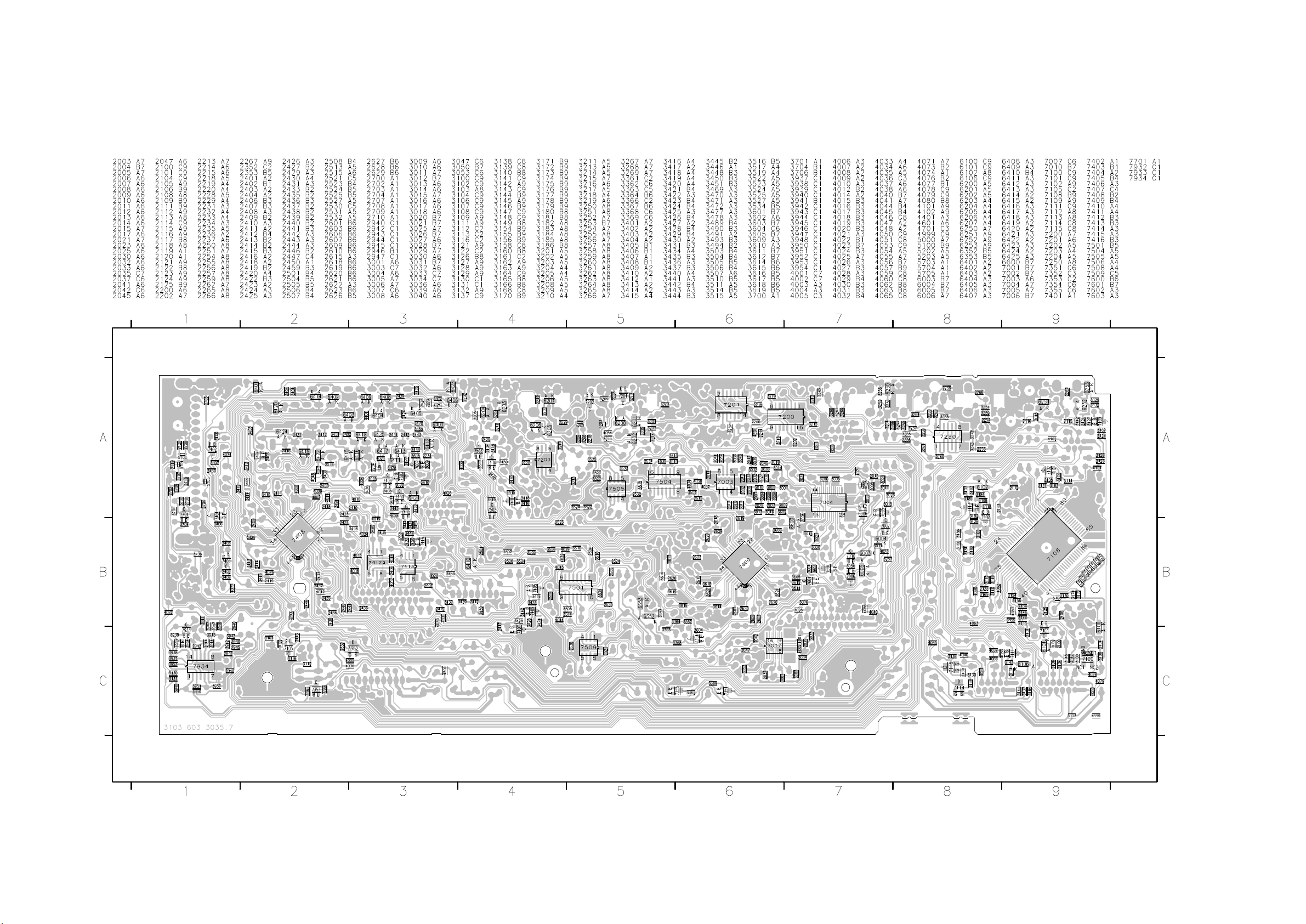
Page 17
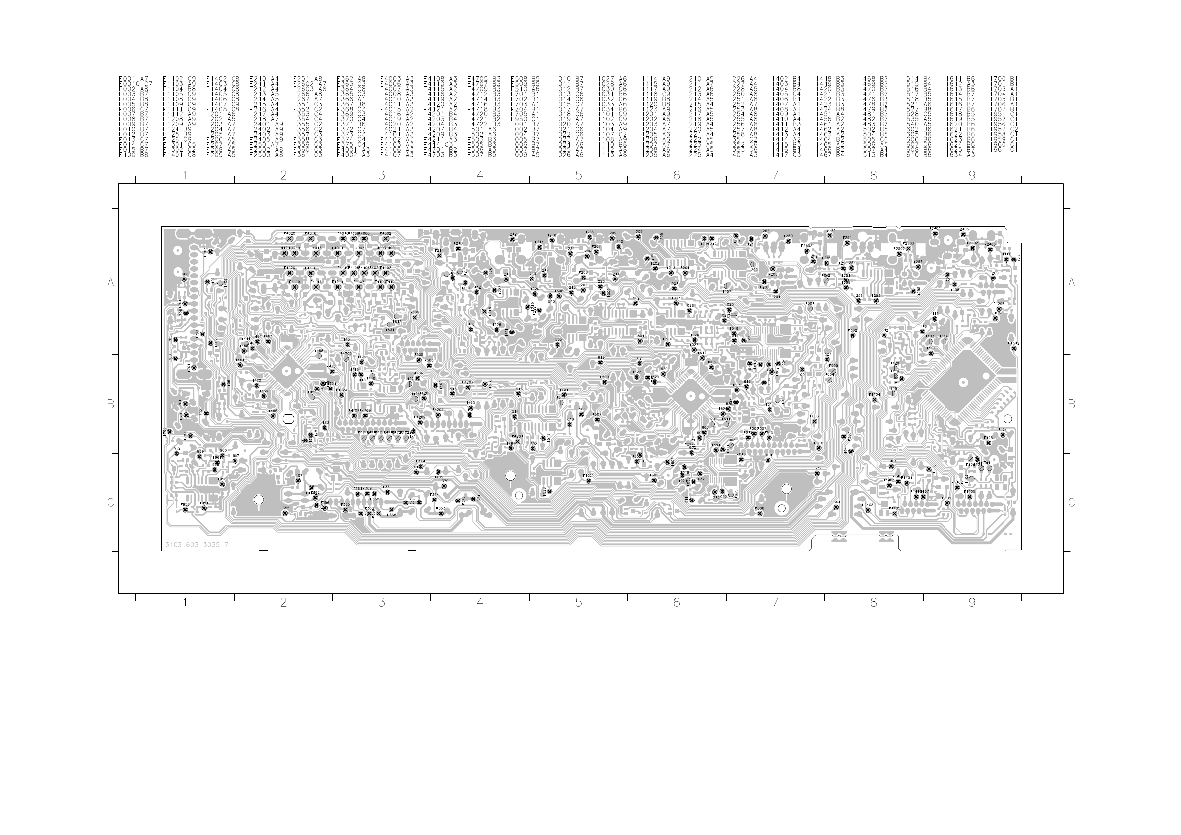
Page 18
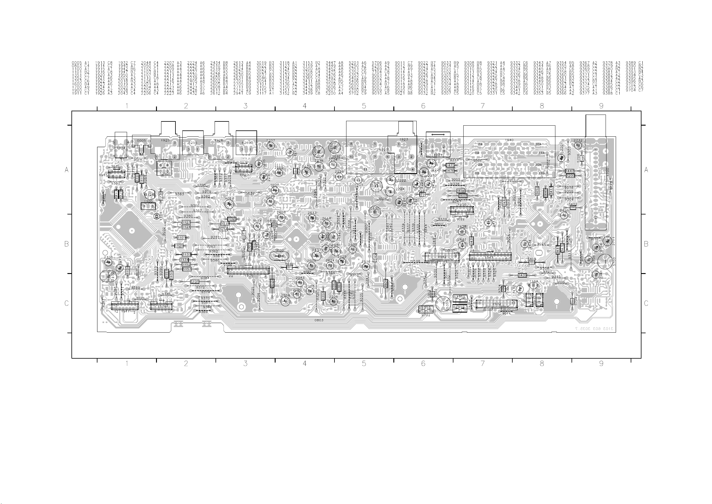
Page 19
Page 20
1
2
3
4 1715
5
6
7
8
9
10
11
12
13
14
16
18
19
20
12
A
+3V3 +3V3
A
B
2
5
22n
C
2101
B
D
PNX7100_SYS_RESETn
E
C
F
MPIO13_IDE1_RESETn
D
G
MPIO14_IEEE1394_RESETn
E
H
MPIO15_DTTM_RESETn
I
F
MPIO16_PROGSCAN_RESETn
J
MPIO31_ANA_RESET
G
K
is prohibited without the written consent of the copyright
owner.
All rights reserved. Reproduction in whole or in parts
MPIO20_VIP_RESETn
H
L
M
MPIO18_IDE2_RESETn
I
N
Alle rechten voorbehouden. Verveelvuldiging, geheel of
toestemming van de auteursrechthebbende.
gedeeltelijk, is niet toegestaan dan met schriftelijke
7106
NCP303LSN29
INP
CD
NC
4
OUTP
GND
3
3117
I114
4115
4116
4K7
1
3187
not used
3114
6100
not used
4K7
3166
3119
4K7
RESETn
EJTAG_RESETn
I100
6101
1PS76SB10
IRESET_DIG
4K7
3165
3163
I119
4K7
3162
I120
4K7
3173
I121
4K7
3184
I122
3041
4K7
not used
I124
4K7
3042
I123
4K7
4K7
3160
I125
4K7
4117
not used
1PS76SB10
3095
4K7
4K7
7104-3
74LVC08AD
9
10
7104-4
74LVC08AD
12
13
7107-1
74LVC08AD
1
2
7107-2
74LVC08AD
4
5
7107-3
74LVC08AD
9
10
7104-1
74LVC08AD
1
2
7104-2
74LVC08AD
4
5
PNX7100_RESETn
I102
470p
2114
I112
714
11
714
714
714
714
714
714
3
4567
89
10 11 12
13 14
1100 A10
1102 B14
1103 H14
VDD_PNX_PAD
3157
47R
3125
4K7
2108
100n
4
2102
7103
74LVC1G32GW
1
2
35
3104
2104
3102
1R0
10p
2105
47R
10p
4124
not used
not used
3111
1R0
10p
MPIO4
2025
10p
3105
1R0
2106
not used
3109
1R0
3115
1R0
10p
2107
10p
2109
3121
10K
3107
1R0
10p
2110
MPIO6_BE_DLOAD
F0011
F0009
F0007
F0005
F0003
F0001
F0508
F0514
F0512
F0511
F0510
F0509
F0503
F0506
2111
10p
10p
F0015
F0501
1100
FMN-BMT
1105
FMN-BMT
15
14
13
12
11
10
9
8
7
6
5
4
3
2
1
15
14
13
12
11
10
9
8
7
6
5
4
3
2
1
RESET_IDE1n
+3V3
MPIO22_IDE1_En
BE_DATA
+3V3
3113
I105
10K
XIO_SEL_NANDFLASH
4122
not used
BE_BCLK
XIO_SEL0
not used
4123
I106
XIO_SEL_NORFLASH
for DTTV only
+3V3+3V3
+3V3_RES
5100
BLMP18P
100n
2103
I108
8
470p
2117
I109
I110
3
2125
RESET_IDE1n
RESET_1394n
RESET_DTTMn
100n
+3V3
RXD3
TXD3
UART2
TXD2
RXD2
RTS2
CTS2
MPIO6_BE_DLOAD
3144
100R
7100
PDTC124EU
3085
100K
MPIO1_ANA_IRQn
BE_FAN
RESET_DTTMn
+5V +5V
3123
4K7
3036
100K
3131
47R
3140
47R
3152
7101
PDTC124EU
BE_DATA_WR
BE_SYNC
BE_FLAG
BE_DATA_RD
BE_WCLK
BE_V4
3136
47R
3139
47R
3141
47R
47R
3044
4K7
not used
ANALOG_RESETn
+3V3
3134
4K7
1106
3127
4K7
not used
4118
not used
MPIO17_HD_ON
F0601
1
2
F0603
3
7102
PDTC124EU
1n5
2124
not used
3045
3150
100R
I111
6
F936
8
3
6
2118
RESET_PROGSCANn
CTS3
RTS3
ANALOG_RESETn
+3V3
not used
VIP_RESETn
RESET_IDE2n
470p
SD-71308
not used
3003
100R
7107-4
74LVC08AD
4K7
not used
3137
100R
3129
12
13
+3V3
4K7
+3V3_RES
714
10
+5V
100K
ION
7111-5
74HCT14D
14
7
3038
7105
PDTC124EU
11
11
4125
12
3132
4K7
SCL0
SDA0
+5V_SERV
14
+5V
4111
not used
7111-6
74HCT14D
7
I117
13
3098
3080
100R
3081
100R
3053
10K
not used
100K
4119
3142
100R
not used
3040
MPIO1_ANA_IRQn
4120
not used
HD_ON
BE_FAN
2120
6K8
not used
4110
100n
4113
5104
BLMP18P
IRESET_DIG
not used
F0410
F0409
F0408
F0407
F0406
F0405
F0404
F0403
F0402
F0401
+5V
1104
FMN-BMT
10
9
8
7
6
5
4
3
2
1
+3V3
3082
TXD0
ANALOG BOARD
RXD0
+3V3
3195
RTS0
CTS0
100K
1
6
100K
3
8
2113
10p
not used
5102
BLMP18P
not used
IDE1_CTL
7111-1
74HCT14D
714
7111-3
74HCT14D
14
7
7111-2
74HCT14D
714
7111-4
74HCT14D
14
RESET_IDE1n
IDE1_DD(15:0)
IDE1_CTL
IDE1_IORDY
4112
I116
2116
2
5
4
9
3054
10K
IDE1_DD(7)
IDE1_DD(8)
IDE1_DD(6)
IDE1_DD(9)
IDE1_DD(5)
IDE1_DD(10)
IDE1_DD(4)
IDE1_DD(11)
IDE1_DD(3)
IDE1_DD(12)
IDE1_DD(2)
IDE1_DD(13)
IDE1_DD(1)
IDE1_DD(14)
IDE1_DD(0)
IDE1_DD(15)
IDE1_DMARQ
IDE1_IORDY
IDE1_IRQ
6103
TLMH3100
100n
+3V3
10K
3039
IDE1_DIOWn
IDE1_DIORn
IDE1_DMACKn
IDE1_DA1
IDE1_DA0
IDE1_DA2
IDE1_CS0n
IDE1_CS1n
3191
100K
-5V
not used
TXD1
RXD1
-5V
VIP_FB
UART0
7
3092
100K
3050 33R
3106
3108 33R
3112 33R
3120 33R
3122 33R
3128 33R
3133 33R
3135 33R
3143 82R
3145 5K6
3156
3161 82R
3164
3168
3180 220R
1
19
2
3
4
5
6
7
8
9
3189
10K
3197
100R
3199
10K
2115
100n
3192
3093
4K7
3EN1
3EN2
G3
2
6K8
6K8
33R3051
33R
33R3110
33R3116
33R3118
33R3124
33R3126
33R3130
33R3138
82R3154
4K7
10K
+3V3
7108
74LVC245APW
20
1
10
3185
100R
2119
F0204
F0206
F0208
F0210
F0212
F0214
F0216
F0218
F0234
F0239
1n5
F0201
F0203
F0205
F0207
F0209
F0211
F0213
F0215
F0217
F0221
18
17
16
15
14
13
12
11
2112
+5V
1n5
3147
22R
3149
BLMP18P
22R
3159
22R
3167
+5V_SERV
10K
3186
5103
F0223
F0225
F0227
F0229
F0231
F0233
F0237
F0236
F0235
33R
3170
33R
F0301
F0302
F0303
F0304
F0305
F0306
F0307
3175
33R
3172
MPIO19_EEPROM_En
IDE1
F0202
1-440090-4
F0238
33R
33R
3178
1103
1
2
3
4
5
6
7
9
8
B7B-PH-SM4-TBT(LF)
Service
1102
1
2
3
4
5
6
7
8
9
10
11
12
13
14
15
16
17
18
19
20
21
22
23
24
25
26
27
28
29
30
31
32
33
34
35
36
37
38
39
40
A
B
C
D
E
F
G
H
I
1104 G9
1105 C10
1106 I5
2025 A8
2101 B1
2102 E7
2103 C3
2104 E8
2105 E8
2106 E8
2107 E8
2108 A7
2109 E9
2110 E9
2111 E9
2112 H13
2113 C11
2114 A2
2115 E12
2116 E11
2117 D3
2118 I3
2119 I12
2120 I8
2124 I5
2125 C4
3003 G6
3036 C6
3038 I6
3039 E11
3040 I8
3041 F2
3042 G2
3044 D7
3045 H5
3050 A12
3051 A12
3053 I8
3054 A12
3080 G7
3081 H7
3082 G10
3085 C6
3092 I11
3093 I12
3095 C2
3098 I7
3102 B8
3104 B7
3105 B8
3106 A12
3107 B9
3108 A12
3109 B8
3110 A12
3111 B8
3112 A12
3113 A3
3114 A2
3115 C8
3116 A12
3117 H2
3118 B12
3119 I2
3120 B12
3121 A9
3122 B12
3123 E6
3124 B12
3125 E7
3126 B12
3127 F5
3128 B12
3129 F6
3130 B12
3131 C7
3132 F7
3133 C12
3134 G5
3135 C12
3136 C7
3137 F6
3138 C12
3139 C7
3140 C7
3141 D7
3142 G8
3143 C12
3144 E5
3145 C12
3147 E13
3149 E13
3150 I6
3152 D7
3154 D12
3156 D12
3157 D7
3159 E13
3160 I2
3161 D12
3162 D2
3163 C2
3164 D12
3165 C2
3166 I2
3167 E13
3168 D12
3170 E13
3172 E13
3173 E2
3175 E14
3178 E14
3180 D12
3184 F2
3185 G12
3186 G13
3187 F2
3189 H12
3191 H11
3192 H12
3195 I10
3197 I12
3199 I12
4112 D11
4113 F9
4115 D2
4116 I2
4117 A2
4118 F5
4119 F8
4120 F8
4122 A4
4123 A4
4124 A8
4125 H7
5100 C4
5102 D11
5103 I13
5104 H8
6100 A2
6101 A2
6103 D11
7100 E5
7101 E6
7102 F5
7103 A8
7104-1 H2
7104-2 I2
7104-3 D2
7104-4 D2
7105 F6
7106 A1
7107-1 E2
7107-2 F2
7107-3 G2
7107-4 H6
7108 E12
7111-1 G11
7111-2 I11
7111-3 H11
7111-4 I11
7111-5 I6
7111-6 I7
F0001 B9
F0003 B9
F0005 B9
F0007 B9
F0009 B9
F0011 B9
F0015 A10
F0201 A13
F0202 B14
F0203 A13
F0204 A13
F0205 A13
F0206 A13
F0207 A13
F0208 A13
F0209 B13
F0210 B13
F0211 B13
F0212 B13
F0213 B13
F0214 B13
F0215 B13
F0216 C13
F0217 C13
F0218 C13
F0221 C13
F0223 C14
F0225 C14
F0227 C14
F0229 D14
F0231 D14
F0233 D14
F0234 D13
F0235 E13
F0236 E13
F0237 E14
F0238 E14
F0239 D13
F0301 H13
F0302 H13
F0303 H13
F0304 H13
F0305 H13
F0306 H13
F0307 I13
F0401 H9
F0402 H9
F0403 G9
F0404 G9
F0405 G9
F0406 G9
F0407 G9
F0408 G9
F0409 F9
F0410 F9
F0501 D10
F0503 D9
F0506 D9
F0508 C9
F0509 D9
F0510 C9
F0511 C9
F0512 C9
F0514 C9
F0601 I5
F0603 I5
F936 G3
I100 A2
I102 A3
I105 A4
I106 B4
I108 D3
I109 E3
I110 E3
I111 F3
I112 C3
I114 C2
I116 D11
I117 H7
I119 D2
I120 E2
I121 E2
I122 F2
I123 H2
I124 G2
I125 I2
A
B
C
D
E
F
G
H
I
J
K
L
M
N
4110 F8
-5V
4111 G7
O
P
1
12345
24
3
5
6
7
67
8
9
10
89
STAGE: LAB 1
DATE: 04-12-01
11
12
10 11 12
AV003477
CLASS_NO
3pc332
1
13
14
2004-11-12
NAME
Ulreich / Linde
2
3
15
IDE1,UARTS,RESET,BE
13 14
DVD+RWSETNAMECHN
CHRY - F 05
SUPERS.
DATEMGr CHECK
2004-09-27********
16
17
12
3103 603 3060
C
KONINKLIJKE PHILIPS ELECTRONICS N.V. 2000
18
19
O
0
2004-12-01
2004-11-050
P
1
***10 130
A2
20
Page 21
2
3
4
5
7
8
96
101 17
11
12
13
14
15
16
18
19
20
A
B
A
C
1203
SR
B
D
DV IN
E
C
F
D
2202
G
E
H
I
F
J
G
K
is prohibited without the written consent of the copyright
owner.
All rights reserved. Reproduction in whole or in parts
+3V3
L
H
M
I
+3V3
N
Alle rechten voorbehouden. Verveelvuldiging, geheel of
gedeeltelijk, is niet toegestaan dan met schriftelijke
toestemming van de auteursrechthebbende.
1234
25266162
INTERFACE
+5V
5201
I206
TLMH3100
3275
330R
I200
PDTC144EU
100n
+3V3_IEEE_PLL
56
PLLVDD
LINK
17186364
7202
100n
2228
6
5
4
3
2
1
F1203
24M576
12p
2212
5204
BLMP18P
1201
CX-8045G
100u
F1205
F1204
F1202
F1201
5200
BLMP18P
5202
BLMP18P
5203
BLMP18P
2217
2203
3232
I210
2201
100n
12p
3253
I201
2207
I202
2209
I203
2214
I204
2218
1%
56R
270p
1R0
2200
1u0
3233
3240
2204
100n
not used
100n
100n
100n
100n
2219
1%
56R
1%
5K1
2210
2215
3283
10K
not used
3205
6K34
1%
56R
3212
2205
100n
100n
100n
2220
100n
1%
3213
F203
2206
100n
+3V3_IEEE_A
I207
40
R0
I208
41 23
R1
I209
38
TPBIAS0
1%
56R
37
TPA0+
36
TPA0-
35
TPB0+
34
TPB0-
59
XI
60
XO
16
43
44
45
NC
46
47
54
55
TEST1
2928
1R0
3261
+3V3_IEEE_PLL
+3V3_IEEE_A
35V4u7
100n
2208
+3V3_IEEE_D
2222
100n
2221
100n
BIAS
VOLTAGE
AND
CURRENT
GENERATOR
XTAL OSC.
PLL
CLOCK
TRANSMIT
DATA
ENCODER
PDI1394P25
TEST0
2223
100n
2224
100n
2225
27
3031425152
TESTM
RECEIVED
DECODER/
ARBITR’N
CONTROL
MACHINE
3339484950
100n
+3V3_IEEE_D
4205
DATA
TIMER
AND
STATE
LOGIC
32
PHY
100n
2226
DVDDAVDD
6200
2227
567
+3V3_IEEE_D +3V3_LINK
not used
10K
3281
3284
1R0
10K
3206
10K
3209
1R0
3220
10R
3225
10R
3231
10R
3236
10R
3242
10R
+3V3_LINK
I211
I212
I218
I219
I222
I225
I226
I227
3248
22R
PCI_AD(31:0)
3263 4K7
3265 4K7
3267
3269 4K7
RESET_1394n
PCI_AD(24)
PCI_AD(25)
PCI_AD(26)
PCI_AD(27)
PCI_AD(28)
PCI_AD(29)
PCI_AD(30)
PCI_AD(31)
4K73262
4K73264
4K73266
4K7
4K73268
2235
1n0
7200
PDI1394P25
CPS
LPS
ISO_
C|LKON
SYSCLK
LREQ
CTL0
CTL1
PC0
PC1
PC2
CNA
RESET_
PLLGNDDGNDAGND
5758
not used
3203
100n
2229
D0
D1
D2
D3
D4
D5
D6
D7
PD
2230
+3V3_IEEE_D
24
15
19
2
1
4
5
6
7
8
9
10
11
12
13
20
21
22
3
53
14
10K
100n
3285
I215
I216
I213
I214
3200
2231
10R
+3V3_IEEE_D
4201
4202
10K
MPIO2_1394_IRQn
2232
100n
100n
+3V3_IEEE_D
10K
3280
2237
100n
3204
10K
MPIO8_1394_CNA
MPIO21_1394_POWERDOWN
+3V3_LINK
MPIO23_1394_LED
2234
2233
100n
100n
3208
3216
10R
3223
10R
3228
10R
3234
10R
3238
10R
3245
10R
+3V3_IEEE_D
+3V3_LINK
3276
1K0
81011
10K
3282
I217
10K
3207
2236
100n
9
138
132
120
113
+3V3_LINK
107
95
90
84
78
LINK
61
70
54
44
35
24
18
12
7201
6
PDI1394L40
12
VDD
82
3297
3298 220R
3299
3316
3317 220R
3318
3319
3273 10R
F201
+3V3_LINK
220R
220R
220R3315
220R
220R
220R
I224
PHYD0
81
PHYD1
80
PHYD2
79
PHYD3
76
PHYD4
75
PHYD5
74
73
86
85
88
91
56
57
55
47
48
92
93
42
PHYD6
PHYD7
PHYCTL0
PHYCTL1
LREQLREQ87
SCLK
LPS
CYCLEIN
CYCLEOUT
CLK50
1394MODE
PD
LINKON
ISON
RESET_
LINK
CORE
12KB BUFFER
MEMORY
ISOCH & ASYNC
PACKETS
AV1
TRANSMITTER / RECEIVER
CONTROL
49
1
50
2
51
3
52
4
58
5
59
6
72
7
71
8
104
9
65
10
66
67
68
105
129
144
130
22
21
20
19
16
15
14
13
10
9
8
7
4
3
2
1
41
RESERVED
11
12
13
14
15
16
17
HIFAD0
HIFAD1
HIFAD2
HIFAD3
HIFAD4
HIFAD5
HIFAD6
HIFAD7
HIFD8
HIFD9
HIFD10
HIFD11
HIFD12
HIFD13
HIFD14
HIFD15
HIFINT_38 HIFMUX
HIFWAIT
131
137
AND
STATUS
REGISTERS
106
112
119
ASYNC
TRANSMITTER
AND
RECEIVER
8-BIT
INTERFACE
94
89
83
77
GND
69
60
AV2
AV2ERR0|LTLEND
AV2ERR1|DATINV
TRANSMITTER / RECEIVER
23
34
43
53
I205
AV1D0
AV1D1
AV1D2
AV1D3
AV1D4
AV1D5
AV1D6
AV1D7
AV1CLK
AV1FSYNC
AV1VALID
AV1SY
AV1SYNC
AV1ENDPCK
AV1ERR0
AV1ERR1
AV1READY
AV2D0
AV2D1
AV2D2
AV2D3
AV2D4
AV2D5
AV2D6
AV2D7
AV2CLK
AV2FSYNC
AV2VALID
AV2SY
AV2SYNC
AV2ENDPCK
AV2READY
TESTPIN
HIFA0
HIFA1
HIFA2
HIFA3
HIFA4
HIFA5
HIFA6
HIFA7
HIFA8
HIFALE
HIF16BIT
11
17
108
109
3211 33R
110
3214 33R
111
114
3217 33R
115
116
117
3222
99
3224 82R
100
3229 33R
102
101
103
3226 33R
98
AV1ENDPCK
96
97
118
133
3237 33R
134
135
3241 33R
136
3243 33R
139
140
3246 33R
141
3247 33R
142
124
3251 33R
125
127
126
128
123
121
122
143
62
1
63
2
64
3
33
32
31
30
29
28
27
26
25
I223
36HIFSC_
I220
37HIFWR_
39
40HIFRD_
45
46
5
I221
33R3210
33R3215
33R3218
33R3221
33R
33R3227
F216
F200
33R3239
33R3244
33R3249
3202 220R
3260
3277
3278 220R
3279
3295
3296
3272
3271 220R
F213
F212
F211
F209
F208
F207
F215
F205
F217
3230
3219 10K
3254 33R
3256 4K7
3257 22K
3250 4K7
3235
F214
10K
220R
220R3274
220R
220R
220R3294
220R
220R
220R
220R3270
4203
not used
4204
F210
F206
F204
MX_D(0)
MX_D(1)
MX_D(2)
MX_D(3)
MX_D(4)
MX_D(5)
MX_D(6)
MX_D(7)
4K73255
4K73259
33R3252
22K3258
+3V3_LINK
L_D(0)
L_D(1)
L_D(2)
L_D(3)
L_D(4)
L_D(5)
L_D(6)
L_D(7)
10K
+3V3_LINK
PCI_AD(0)
PCI_AD(1)
PCI_AD(2)
PCI_AD(3)
PCI_AD(4)
PCI_AD(5)
PCI_AD(6)
PCI_AD(7)
PCI_AD(8)
BOARD_ID
4K7
3286
not used
MPIO9_BOARD_ID_0
MPIO10_BOARD_ID_1
MPIO11_HDMI_RESETn
MPIO12_HDMI_IRQ
4K7
3290
13 14
L_D(7:0)
L_CLK
L_FSYNC
L_VAL
L_SYNC
L_D_CTL
MX_D(7:0)
MX_D_CTL
MX_CLK
MX_VAL
MX_SYNC
+3V3_LINK
PCI_AD(31:0)
+3V3_LINK
10K
3314
XIO_SEL1
PCI_CBE(1)
PCI_CBE(2)
+3V3
3287
3291
4K7
4K7
3288
3292
4K7
4K7
3289
3293
4K7
not used
4K7
A
B
C
D
E
F
G
H
I
1201 D1
1203 B1
2200 B2
2201 C2
2202 D1
2203 D2
2204 D2
2205 D2
2206 G3
2207 F2
2208 G3
2209 G2
2210 G2
2212 H1
2214 H2
2215 H2
2217 I2
2218 I2
2219 I2
2220 I2
2221 I3
2222 I3
2223 I3
2224 I4
2225 I4
2226 I4
2227 I4
2228 I5
2229 I5
2230 I5
2231 I6
2232 I6
2233 I6
2234 I6
2235 A5
2236 A9
2237 B6
3200 E6
3202 F12
3203 H5
3204 D6
3205 A2
3206 A7
3207 A8
3208 B7
3209 B8
3210 B12
3211 B12
3212 B2
3213 B3
3214 B12
3215 C12
3216 B7
3217 C12
3218 C12
3219 C12
3220 B7
3221 C12
3222 C12
3223 B7
3224 C12
3225 C7
3226 C12
3227 C12
3228 C7
3229 C12
3230 C12
3231 C7
3232 C2
3233 C2
3234 C7
3235 C13
3236 C7
3237 D12
3238 C7
3239 D12
3240 C2
3241 D12
3242 C7
3243 D12
3244 D12
3245 D7
3246 D12
3247 D12
3248 D7
3249 D12
3250 E12
3251 D12
3252 E12
3253 D2
3254 E12
3255 E12
3256 E12
3257 E12
3258 E12
3259 E12
3260 F12
3261 E3
3262 F7
3263 F7
3264 F7
3265 F7
3266 F7
3267 F7
3268 F7
3269 G7
3270 F12
3271 F12
3272 F12
3273 G8
3274 F12
3275 G5
3276 G7
3277 F12
3278 F12
3279 F12
3280 A7
3281 A7
3282 A8
3283 A2
3284 A8
3285 A6
3286 H13
3287 H13
3288 H13
3289 H13
3290 I13
3291 I13
3292 I13
3293 I13
3294 F12
3295 F12
3296 F12
3297 E8
3298 F8
3299 F8
3314 F13
3315 F8
3316 F8
3317 F8
3318 F8
3319 F8
4201 D6
4202 D6
4203 G12
4204 G12
4205 A4
5200 F2
5201 F4
5202 G2
5203 H2
5204 I1
6200 G4
7200 A5
7201 B12
7202 H5
F1201 B2
F1202 B2
F1203 B1
F1204 B2
F1205 B2
F200 C12
F201 C9
F203 C3
F204 C13
F205 C12
F206 C13
F207 C13
F208 C12
F209 C12
F210 C13
F211 B13
F212 B12
F213 B12
F214 C12
F215 C12
F216 C12
F217 C12
I200 H4
I201 F2
I202 G2
I203 H2
I204 I2
I205 G11
I206 G4
I207 A3
I208 A3
I209 B3
I210 C2
I211 B7
I212 B7
I213 D6
I214 D6
I215 A6
I216 B6
I217 A8
I218 C7
I219 C7
I220 F12
I221 F12
I222 C7
I223 F12
I224 G8
I225 C7
I226 C7
I227 C7
A
B
C
D
E
F
G
H
I
J
K
L
M
N
O
P
1
12
2
37
4
3
5
45678
6
8
9
10
11
91011
AV003477
CLASS_NO
STAGE: LAB 1
DATE: 04-12-01
12
13
14
3pc332
2004-11-12
NAME
1
2
3
Voko / Linde
15
12
13 14
DVD+RWSETNAMECHN
CHRY - F 05
1394
SUPERS.
DATEMGr CHECK
2004-09-27********
16
17
12
3103 603 3060
C
KONINKLIJKE PHILIPS ELECTRONICS N.V. 2000
18
19
O
0
2004-12-01
2004-11-050
P
2
***10 130
A2
20
Page 22
1
A
B
A
C
B
D
2303
C
All rights reserved. Reproduction in whole or in parts
is prohibited without the written consent of the copyright
owner.
E
4u7
2305
100n
2
1
2302
2u2
3300
56R
2306
100n
3303
220K
3
2345
7301
74HCT9046AD
4
10
13
15
2
5
RX
M6
EN5
6
6
4
I300
16
[PLL]
EN
G
CX
RX
Af
1
1&
R
Z4
=1
Z3
=1
18
3
4
S
S
5
6
7
11
12
9
14
3
2300
4u7
5
2301
4301
5300
BLMP18P
100n
2304
4303
4309
68p
+5V
3304
4K7
6
3301
3305
3K3
2K2
3302
3306
12K
1R0
7
VDD_PLL_BUF
MPIO25_ADC_FSCLKE_OEn
VDD_PLL_BUF
10K
3311
8
9
10
67
4304
not used
3307
10K
4302
WS012_OUT
4314
VDD_PLL_BUF
7302
74LVC1G125GW
2
1
EN
5
4
3
not used
not used
VDD_PLL_BUF
7300-1
74LVC125AD
2
1
EN
not used
4305
4310
4312
14
7
4313
11 12
89
PLL_OUT
FSCLK3_OUT
FSCLKE_IN_PNX
FSCLK012_OUT
3
WSE_IN
A
B
C
13
2300 B3
2301 B4
2302 C1
2303 C1
2304 B4
2305 C1
2306 C1
2308 E1
2310 E2
3300 C1
3301 C4
3302 C5
3303 D2
3304 C4
3305 C4
3306 C5
3307 B6
3311 C5
4009 E7
4010 E6
4300 E8
4301 C4
4302 B6
4303 C4
4304 A7
4305 A8
4309 C4
4310 B8
4311 E5
4312 C8
4313 D8
4314 A7
4316 D8
5300 A4
5302 E2
7300-1 C7
7300-2 D7
7300-3 E6
7300-4 E7
7301 B2
7302 A7
I300 A2
I303 E6
I305 E2
I306 E6
A
B
C
D
E
F
G
D
E
VDD_PLL_BUF
2308
100n
I305
2310
5302
BLMP18P
100n
+3V3
SCKE_IN
SCK3_OUT
SCK012_OUT
not used
I306
SCK012_OUT
7300-3
74LVC125AD
9
10
4010
not used
14
EN
7
7300-2
74LVC125AD
5
4
7300-4
74LVC125AD
8
4009
11
EN
14
7
4300
not used
14
EN
7
12
13
F
6
SCKE_IN
PLL_OUT
4316
FSCLKE_IN_PNX
D
G
MPIO25_ADC_FSCLKE_OEn
E
H H
gedeeltelijk, is niet toegestaan dan met schriftelijke
Alle rechten voorbehouden. Verveelvuldiging, geheel of
toestemming van de auteursrechthebbende.
12
3
4311
I303
MPIO26_ADC_FWSCLK012_OEn
45678
AV003477
CLASS_NO
DVD+RWSETNAMECHN
STAGE: LAB 1
3pc332
CHRY - F 05
9
FSCLKE_IN
II
0
2004-12-01
2004-11-050
J
1
DATE: 04-12-01
1
3103 603 3060
2004-11-12
NAME
2 13
3
4
5
6
7
Kabinger / Linde
8
2
3
Audio PLL
SUPERS.
DATEMGr CHECK
2004-09-27********
9
10
12
3
C
KONINKLIJKE PHILIPS ELECTRONICS N.V. 2000
11
12
***10 130
J
A3
Page 23
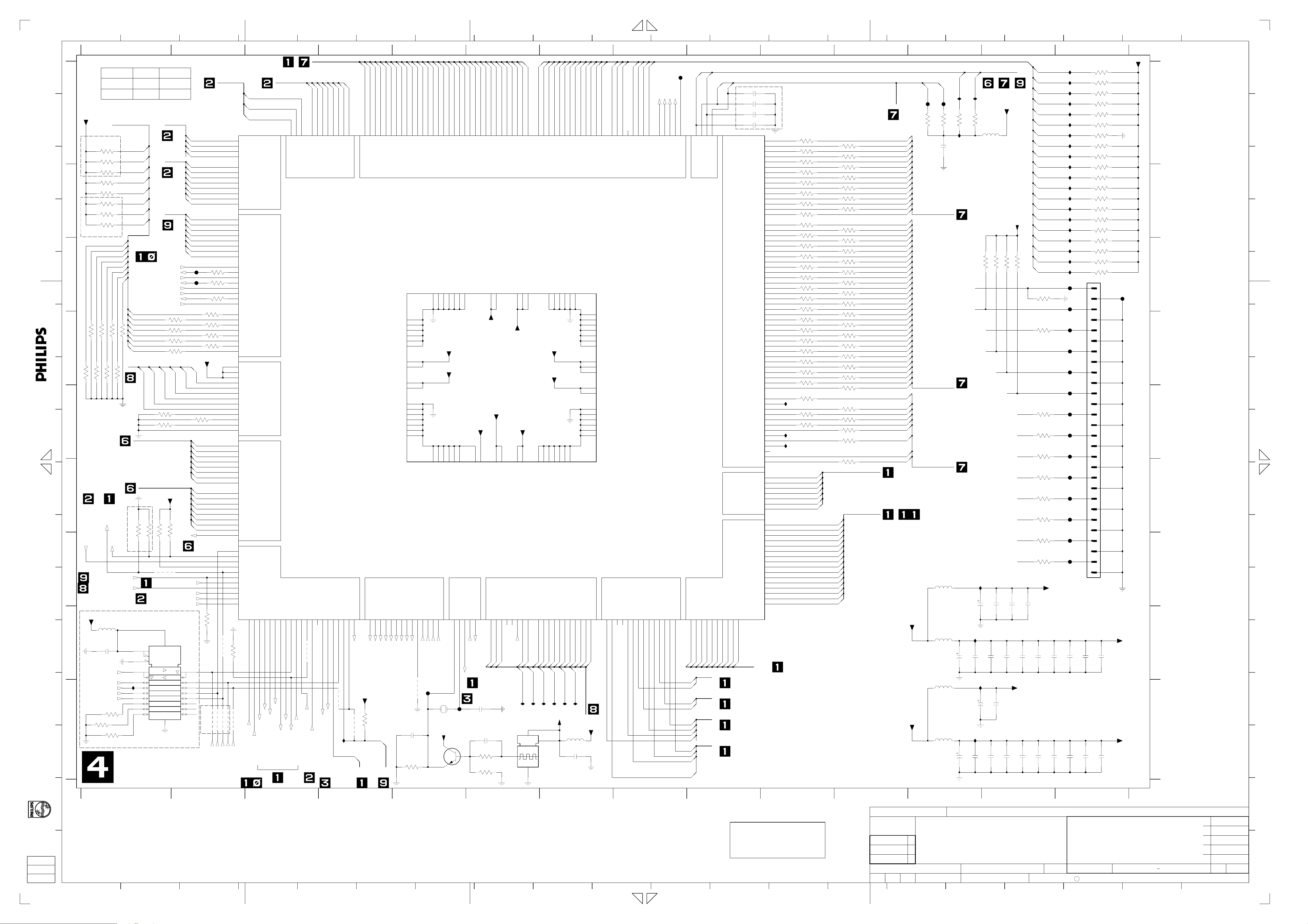
1
2
3
4
5
6
7
8
9
10
11
12
13
14
15 16
17
18
19
20
1234
SDRAM
A
*
32 MB
64 MB
VDD_PNX_PAD
not used
4K7
4K7
4K7
4K7
4K7
4K7
4K7
4K7
ITU_OUT(0)
ITU_OUT(1)
ITU_OUT(2)
ITU_OUT(3)
ITU_OUT(5)
ITU_OUT(4)
*
3828
3829
3830
3831
3832
3833
3834
3835
not used
4K73821
ITU_OUT(7:0)
ITU_OUT(0)
ITU_OUT(1)
ITU_OUT(2)
ITU_OUT(3)
ITU_OUT(4)
ITU_OUT(5)
ITU_OUT(6)
ITU_OUT(7)
PNX7100_ITU_OUT_CLK
ITU_OUT(7)
ITU_OUT(6)
4K73827
B
C
D
E
A
B
C
F
3825 4K7
D
3823 4K7
*
4K73824
4K73822
VIDEO_OUT
G
3820 4K7
3826 4K7
not used
E
H
I
F
MPIO4
J
MPIO2_1394_IRQn
MPIO1_ANA_IRQn
G
MPIO5_VIP_ERROR
MPIO7_MUTE_LVn
K
+3V3
is prohibited without the written consent of the copyright
owner.
All rights reserved. Reproduction in whole or in parts
H
L
MPIO19_EEPROM_En
M
MPIO4_IDE2_IRQ
I
5403
BLM18P
2432
100n
CTS0
CTS1
IDE1_IRQ
3837
10K
3838
10K
3839
10K
I402
N
gedeeltelijk, is niet toegestaan dan met schriftelijke
toestemming van de auteursrechthebbende.
Alle rechten voorbehouden. Verveelvuldiging, geheel of
12
O
3831
3823
-
X
L_D_CTL
L_D(7:0)
ITU_IN(7:0)
PNX7100_HS_IN
PNX7100_HS_OUT
PNX7100_VS_IN
PNX7100_VS_OUT
PNX7100_ITU_IN_FID
PNX7100_ITU_IN_CLK
PNX7100_ITU_IN_VAL
ITU_OUT(0)
ITU_OUT(1)
ITU_OUT(2)
ITU_OUT(3)
ITU_OUT(4)
ITU_OUT(5)
ITU_OUT(6)
ITU_OUT(7)
Y_OUT
C_OUT
CVBS_OUT
3433 1K2
Y(0:7)
CbCr(0:7)
VDD_PNX_PAD
3452
not used
10K
7401
74LVC245APW
1
19
2
3
4
5
6
7
8
9
349910K
3441
10K
4405
not used
MPIO6_BE_DLOAD
MPIO8_1394_CNA
MPIO9_BOARD_ID_0
MPIO10_BOARD_ID_1
not used
20
3EN1
3EN2
G3
2
10
X
-
R_OUT
1%
15R3435
P_CLK
10K 3498
1
L_CLK
L_VAL
L_SYNC
L_FSYNC
L_D(0)
L_D(1)
L_D(2)
L_D(3)
L_D(4)
L_D(5)
L_D(6)
L_D(7)
ITU_IN(0)
ITU_IN(1)
ITU_IN(2)
ITU_IN(3)
ITU_IN(4)
ITU_IN(5)
ITU_IN(6)
ITU_IN(7)
F403
3450 10R
F404
3451 10R
3603 33R
3442 22R
22R3443
3444 22R
22R3445
3446 22R
22R3447
3448 22R
22R3449
VDD_PNX_ANA
B_OUT
G_OUT
3434 15R
Y(0)
Y(1)
Y(2)
Y(3)
Y(4)
Y(5)
Y(6)
Y(7)
CbCr(0)
CbCr(1)
CbCr(2)
CbCr(3)
CbCr(4)
CbCr(5)
CbCr(6)
CbCr(7)
3850
18
17
16
15
14
13
12
11
for C3 only
MPIO19_EEPROM_En
MX_D_CTL
10K
4404
4409
4407
4408
4406
IDE1_IRQ
MPIO4_IDE2_IRQ
7400
PNX7100EH/G/C3
A1
L-CLK
C1
L-VAL
A2
L-SYNC
B1
L-FSYNC
B2
L-D0
C2
L-D1
A3
L-D2
B3
L-D3
C3
L-D4
A4
L-D5
B4
L-D6
C4
L-D7
D3
ITU-IN0
D2
ITU-IN1
E2
ITU-IN2
D1
ITU-IN3
E3
ITU-IN4
E1
ITU-IN5
F4
ITU-IN6
F1
ITU-IN7
F2
HS-IN
T3
HS-OUT
F3
VS-IN
T2
VS-OUT
G4
ITU-IN-FID
G2
ITU-IN-CLK
T4
ITU-OUT-CLK
G3
ITU-IN-VAL
V1
ITU-OUT0
V2
ITU-OUT1
V3
ITU-OUT2
V4
ITU-OUT3
U1
ITU-OUT4
U2
ITU-OUT5
U3
ITU-OUT6
U4
ITU-OUT7
M3
AVDD0
P1
AVDD1
R3
AVDD2
R2
G
T1
B
P3
R-CVBS
N1
Y-CVBS
N3
C-CVBS
P2
CVBS
M2
RSET
N2
IDUMP0
R1
IDUMP1
M1
VREF
J4
PROGY-OUT0
K1
PROGY-OUT1
K2
PROGY-OUT2
K3
PROGY-OUT3
K4
PROGY-OUT4
L1
PROGY-OUT5
L2
PROGY-OUT6
L3
PROGY-OUT7
J3
PROGC-OUT0
J2
PROGC-OUT1
J1
PROGC-OUT2
H4
PROGC-OUT3
H3
PROGC-OUT4
H2
PROGC-OUT5
H1
PROGC-OUT6
G1
PROGC-OUT7
L4
PROG-OUT-CLK
W1
PIO0
W2
PIO1
W3
PIO2
W4
PIO3
Y1
PIO4
Y2
PIO5
Y3
PIO6
Y4
PIO7
AA1
PIO8
AA2
PIO9
AA3
PIO10
AA4
10K
3851
not used
4410
not used
CTS0
CTS1
MX_D(7:0)
MX_VAL
MX_SYNC
MX_CLK
A5
MX-CLK
1394 INDIGITAL VIDEO INTERFACEANALOG VIDEOPROG SCAN
PIOS TEST GENERAL DIGITAL AUDIO INTERFACE UARTS
PIO11
PIO12
PIO13
PIO14
PIO15
PIO16
PIO17
PIO18
PIO19
AB1
AB2
AB3
AC1
AC2
AC3
AD1
AD2
MPIO17_HD_ON
MPIO16_PROGSCAN_RESETn
MPIO15_DTTM_RESETn
MPIO14_IEEE1394_RESETn
MPIO13_IDE1_RESETn
MPIO11_HDMI_RESETn
MPIO12_HDMI_IRQ
MPIO22_IDE1_En
MPIO18_IDE2_RESETn
3
PCI_AD(31:0)
MX_D(0)
MX_D(1)
MX_D(2)
MX_D(3)
MX_D(4)
A6
C5
B5
MX-D0B6MX-D1C6MX-D2A7MX-D3B7MX-D4C7MX-D5
MX-VAL
MX-SYNC
PIO20
PIO21
PIO22
POIO24
PIO23
PIO25
PIO26
PIO27
AE1
AE2
AD3
AD4
4411
for 2004 only
MPIO20_VIP_RESETn
MPIO21_1394_POWERDOWN
MPIO23_1394_LED
AF1
AE3
AE4
AE5
MPIO25_ADC_FSCLKE_OEn
MPIO26_ADC_FWSCLK012_OEn
MX_D(5)
MX_D(6)
MX_D(7)
D7
MX-D6D8MX-D7
PIO28
PIO29
AF4
AF2
AF3
4403
not used
I403
RTS0
PCI_AD(0)
PCI_AD(1)
PCI_AD(2)
PCI_AD(3)
B9
C9
A8
A9
PCI-AD2
PCI-AD3
PCI-AD0
PCI-AD1
PIO30
PIO31
DSU-CLK
DSU-TPC0
DSU-TPC1
AF5
MPIO31_ANA_RESET
4402
UART0
AF8
AF6
AD7
PNX7100_DSU_CLK
PNX7100_DSU_TPC1
+3V3
PNX7100_TDO_DSU_TPC0
3497
100K
RTS1
UART1
4
PCI_AD(4)
PCI_AD(5)
A10
B10
PCI-AD4
PCI-AD5
GND1
GND2
GND3
GND4
GND5
GND6
VDDP1
VDDP2
VDDC1
VDDC2
GND7
GND8
GND9
GND10
GND11
GND12
GND13
PCST0-0
PCST0-1
AF7
AC8
PNX7100_PCST0(0)
PNX7100_PCST0(1)
PCI_AD(9)
PCI_AD(6)
PCI_AD(7)
PCI_AD(8)
C10
D10
B11
C11
PCI-AD6
PCI-AD7
PCI-AD8
PCI-AD9
D4
E4
L11
M11
N11
N12
M4
N4
P4
R4
P11
P12
R11
R12
T11
AB4
AC4
PCST0-2
PCST1-0
PCST1-1
PCST1-2
AE7
AE6
AD6
AD5
PNX7100_PCST0(2)
PNX7100_PCST1(0)
PNX7100_PCST1(2)
PNX7100_PCST1(1)
2430
15p
not used
3862
330R
5
PCI_AD(10)
PCI_AD(11)
PCI_AD(12)
PCI_AD(13)
PCI_AD(14)
A12
B12
C12
A13
B13
PCI-AD10
PCI-AD11
PCI-AD12
PCI-AD13
PCI-AD14
GND51
GND52
D5
VDD_PNX_PAD
VDD_PNX_CORE
AC5
GND14
GND15
GND|TCK-PALM
TCK
TDI
TMS
TRST
AE8
AC7
AD8
AC9
AD9
PNX7100_TDI
PNX7100_TCK
PNX7100_TMS
F405
4401
1401
HC-49/S
not used
+3V3_7402
5
PCI_AD(15)
PCI_AD(16)
PCI_AD(17)
PCI_AD(18)
PCI_AD(19)
C13
D16
C17
B17
A18
PCI-AD15
PCI-AD16
PCI-AD17
PCI-AD18
PCI-AD19
GND50
D6
L12
GND48
GND49
L13
M12
GND46
GND47
M13
VDD_PNX_PLL
AC6
P13
R13
T12
T13
GND16
GND17
GND18
GND19
PLL-OUT
XTAL-IN
XTAL-OUT
AF9
AF10
AE10
PNX7100_TRST
PNX7100_XTAL_IN
PNX7100_XTAL_OUT
PLL_OUT
F406
4M
7403
BC847BW
PCI_AD(20)
D17
PCI-AD20
N13
PCI_AD(24)
PCI_AD(21)
PCI_AD(22)
PCI_AD(23)
C18
B18
A19
B19
PCI-AD21
PCI-AD22
PCI-AD23
PCI-AD24
VDDP9
VDD_PNX_PAD
VDD_PNX_PAD
AC11
AC10
AVSS-CLK
AVDD-CLK
RESETN
SYS-RESETN
SCKE-IN
AE9
AD10
AD11
SCKE_IN
PNX7100_RESETn
PNX7100_SYS_RESETn
2431
15p
not used
2434
33p
3861
1K2
3863
4K7
67
PCI_GNT
A22
CTS2
AE18
AE19
PCI_REQ
PCI_INTA
A23
C22
PCI-GNT
PCI-REQ
PCI-INTA
DTR3
DCD3
CTS3
AF18
AD20
AC20
A24
PCI-CLK
RTS2
PCI_AD(25)
PCI_AD(26)
PCI_AD(27)
PCI_AD(28)
PCI_AD(29)
C20
B20
A21
D20
C21
PCI-AD25
PCI-AD26
PCI-AD27
PCI-AD28
PCI-AD29
PCI/XIO1394 OUT
VDDP8
D12
D11
VDD_PNX_CORE
VDDC9
VDD_PNX_CORE
AC12
AC13
VDDP3
VDDP4
VDDC3
WSE-IN
WSK-IN
SDE-IN
SDK-IN
FSCLKE-IN
AF11
AE12
AD12
SDE_IN
7402
FXO-34FL
3
AF12
FSCLKE_IN_PNX
I407
AE11
WSE_IN
6
PCI_CBE(1)
PCI_CBE(0)
PCI_AD(30)
PCI_AD(31)
A11
B22
PCI-AD31
VDDC7
D15
A14
PCI-CBE0
B21
PCI-AD30
VDDC8
D13
D14
VDD_PNX_PAD
VDD_PNX_CORE
AC14
AC15
P14
GND20
VDDC4
SPDIF1-IN
SPDIF2-IN
FSCLK3-OUT
AF13
AE13
AD14
AD13
SCK3_OUT
FSCLK3_OUT
SPDIF_OPT_IN
SPDIF_COAX_IN
SD1_OUT
SD3_OUT
I408
I409
4
2
4M0
PCI_CBE(3)
PCI_CBE(2)
PCI_DEVSEL
A17
C19
A16
PCI-CBE1
PCI-CBE2
PCI-CBE3
GND44
GND45
L15
L14
R14
R15
T14
GND21
GND22
GND23
WS3-OUT
SCK3-OUT
SD0-OUT
AF16
AE14
AD15
SD1_OUT
SD0_OUT
WS3_OUT
SD2_OUT
FSCLK3_OUT
I410
+3V3_7402
1
PCI_PAR
PCI_IRDY
PCI_TRDY
PCI_IDSEL
PCI_FRAME
C16
C15
B16
D18
PCI-IRDY
PCI-TRDY
PCI-IDSEL
PCI-FRAME
PCI-DEVSEL
GND40
GND41
GND42
GND43
D22
D21
N14
M14
T15
AC21
AC22
GND24
GND25
GND26
SD1-OUT
AE15
SD2_OUT
SCK3_OUT
I411
SCK012-OUT
SD2-OUT
SD3-OUT
FSCLK012-OUT
AF15
AF14
AC16
FSCLK012_OUT
SD3_OUT
SCK012_OUT
WS3_OUT
I412
AC23
PCI_STOP
PCI_SERR
PCI_PERR
B14
B15
C14
A15
PCI-PAR
PCI-STOP
PCI-PERR
PCI-SERR
D23
GND39
E23
GND38
L16
GND37
M15
GND36
M16
GND35
N15
GND34
N16
GND33
M23
VDDP7
N23
VDDP6
P23
VDDP5
R23
VDDC6
T23
VDDC5
P15
GND32
P16
GND31
R16
GND30
T16
GND29
AB23
GND28
GND27
WS012-OUT
SPDIF-OUT
AE16
AD16
SPDIF_OUT
WS012_OUT
DIGITAL_AUDIO
+3V3
5404
BLMP18P
2433
100n
7 8 9 1011121314
8 9 10 11 12
PCI_CON
IIC0
SCL0
SDA1
A26
B26
SCL0
SCL1
SDA1
IDE-DIOR
IDE-DIOW
IDE-IORDY
IDE-DA2
AF26
AE25
AD25
AD26
IDE1_DA2
IDE1_DIOWn
IDE1_DIORn
IDE1_IORDY
IIC1
2400
SCL1
2401
2435 100p
SDRAM-ADDR0
SDRAM-ADDR1
SDRAM-ADDR2
SDRAM-ADDR3
SDRAM-ADDR4
SDRAM-ADDR5
SDRAM-ADDR6
SDRAM-ADDR7
SDRAM-ADDR8
SDRAM-ADDR9
SDRAM-ADDR10
SDRAM-ADDR11
SDRAM-ADDR12
SDRAM-ADDR13
SDRAM-ADDR14
SDRAM-DATA0
SDRAM-DATA1
SDRAM-DATA2
SDRAM-DATA3
SDRAM-DATA4
SDRAM-DATA5
SDRAM-DATA6
SDRAM-DATA7
SDRAM-DATA8
SDRAM-DATA9
SDRAM-DATA10
SDRAM-DATA11
SDRAM-DATA12
SDRAM-DATA13
SDRAM-DATA14
SDRAM-DATA15
SDRAM-DATA16
SDRAM-DATA17
SDRAM-DATA18
SDRAM-DATA19
SDRAM-DATA20
SDRAM-DATA21
SDRAM-DATA22
SDRAM-DATA23
SDRAM-DATA24
SDRAM-DATA25
SDRAM-DATA26
SDRAM-DATA27
SDRAM-DATA28
SDRAM-DATA29
SDRAM-DATA30
SDRAM-DATA31
IDE BE-1 SDRAM
IDE-CS0
IDE-CS1
IDE-DA0
IDE-DA1
AB26
AE26
AC26
IDE1_CS1n
IDE1_CS0n
IDE1_DA1
IDE1_DA0
100p
100p
100p2402
CAS0
CAS1
DQM0
DQM1
DQM2
DQM3
RAS0
RAS1
WE0
WE1
RP
CKE
HSCKB
BE-BCLK
BE-DATI
BE-DATO
BE-FLAG
BE-SYNC
BE-V4
BE-WCLK
IDE-DD0
IDE-DD1
IDE-DD2
IDE-DD3
IDE-DD4
IDE-DD5
IDE-DD6
IDE-DD7
IDE-DD8
IDE-DD9
IDE-DD10
IDE-DD11
IDE-DD12
IDE-DD13
IDE-DD14
IDE-DD15
IDE_CTL
N26
P25
R24
P26
P24
N25
M26
M24
L25
L23
N24
L24
K23
L26
M25
C25
D24
D26
E25
F23
F25
G23
G25
G26
G24
F26
F24
E26
E24
D25
C26
T25
U23
U25
V23
V25
W23
W25
Y26
W26
W24
V26
V24
U26
U24
T26
T24
H26
J25
H23
H24
R26
R25
J23
J26
H25
J24
K24
K25
K26
AA23
AA26
Y25
AA24
AA25
Y23
Y24
AC24
AE24
AD23
AF23
AE22
AD21
AF21
AF20
AE20
AE21
AF22
AD22
AE23
AF24
AD24
AB24
not used
3457
3459 22R
3465 22R
3467
3470
3472
3474 22R
3480 22R
3482 22R
3488
3490 22R
3494 22R
3496 22R
3840 22R
I404
3857 22R
I405
I406
BE_BCLK
BE_DATA_RD
BE_DATA_WR
BE_FLAG
BE_SYNC
BE_V4
BE_WCLK
22R3453
3454 22R
22R3455
3456 22R
22R
22R3461
3462 22R
22R3463
3464 22R
22R
22R3468
3469 22R
22R
3471 22R
22R
22R3476
22R3478
3479 22R
22R3484
3485 22R
22R3486
3487 22R
22R
22R3492
3493 22R
22R3853
22R3855
3856 22R
3858 22R
3859 22R
IDE1_DD(0)
IDE1_DD(1)
IDE1_DD(2)
IDE1_DD(3)
IDE1_DD(4)
IDE1_DD(5)
IDE1_DD(6)
IDE1_DD(7)
IDE1_DD(8)
IDE1_DD(9)
IDE1_DD(10)
IDE1_DD(11)
IDE1_DD(12)
IDE1_DD(13)
IDE1_DD(14)
IDE1_DD(15)
UART0: DEBUG / SERVICE
UART1: DEV ONLY
UART2: DTTM
UART3: G-LINK
22R3458
22R3460
SDRAM_ADDR(10)
SDRAM_ADDR(11)
SDRAM_ADDR(12)
22R3466
SDRAM_ADDR(13)
SDRAM_ADDR(14)
22R3473
22R3475
22R3477
SDRAM_DATA(10)
SDRAM_DATA(11)
SDRAM_DATA(12)
22R3481
SDRAM_DATA(13)
SDRAM_DATA(14)
22R3483
SDRAM_DATA(15)
SDRAM_DATA(16)
SDRAM_DATA(17)
SDRAM_DATA(18)
SDRAM_DATA(19)
SDRAM_DATA(20)
22R3489
SDRAM_DATA(21)
SDRAM_DATA(22)
22R3491
SDRAM_DATA(23)
SDRAM_DATA(24)
SDRAM_DATA(25)
SDRAM_DATA(26)
22R3495
SDRAM_DATA(27)
SDRAM_DATA(28)
22R3836
SDRAM_DATA(29)
SDRAM_DATA(30)
22R3852
SDRAM_DATA(31)
22R3854
33R3860
BE_DATA
IDE1_DD(15:0)
SDRAM_ADDR(0)
SDRAM_ADDR(1)
SDRAM_ADDR(2)
SDRAM_ADDR(3)
SDRAM_ADDR(4)
SDRAM_ADDR(5)
SDRAM_ADDR(6)
SDRAM_ADDR(7)
SDRAM_ADDR(8)
SDRAM_ADDR(9)
SDRAM_ADDR(14:0)
SDRAM_DATA(0)
SDRAM_DATA(1)
SDRAM_DATA(2)
SDRAM_DATA(3)
SDRAM_DATA(4)
SDRAM_DATA(5)
SDRAM_DATA(6)
SDRAM_DATA(7)
SDRAM_DATA(8)
SDRAM_DATA(9)
SDRAM_DATA(31:0)
CAS(0)
DQM(0)
DQM(1)
DQM(2)
DQM(3)
RAS(0)
WE(0)
CKE
HSCKB
+3V3
+1V8
CHN SETNAME DVD+RW
AV003477
PCI_GNTA
PCI_REQA
PCI_GNTB
PCI_REQB
B23
C23
B24
C24
PCI-GNTA
PCI-REQA
PCI-REQB
RTS3
RXD0
RXD1
AF19
AE17
AC17
AC18
XIO_SEL1
XIO_SEL0
B8
C8
XIO-SEL0
PCI-GNTB
RXD2
RXD3
TXD0
AF17
AC19
AD17
F402
XIO_SEL2
XIO_ACK
A20
D19
D9
XIO-ACK
XIO-SEL1
XIO-SEL2
TXD1
TXD2
TXD3
AD18
AD19
TXD0
RXD0
TXD1
RXD1
TXD2
RXD2
RTS2
CTS2
TXD3
RXD3
RTS3
CTS3
SDA0
XIO_A25
A25
XIO-A25
IDE-DMARQ
AF25
AB25
IDE1_DMACKn
IDE1_DMARQ
B25
SDA0
I2C
IDE-DMACK
AC25
SDA1
F401
F400
3K3
3405
2403
PNX7100_TDO_DSU_TPC0
SDRAM_CTRL
5401
BLM31
5402
BLM31
5405
BLM31
5406
BLM31
SDA0
SCL1
I438
3K3
3K3
3407
3406
I413
100n
PNX7100_TRST
PNX7100_TDI
PNX7100_TMS
2408
2420
SCL0
I439
3K3
3408
5400
BLMP18P
3425
10K
PNX7100_TCK
EJTAG_RESETn
PNX7100_PCST0(0)
PNX7100_PCST0(1)
PNX7100_PCST0(2)
PNX7100_DSU_CLK
PNX7100_DSU_TPC1
PNX7100_PCST1(0)
PNX7100_PCST1(1)
PNX7100_PCST1(2)
I414
10u
2405
2404
I415
10u
I417
10u
2409
I416
2418
2421
100n
100n
2410
10u
2422
2419
13 14
+3V3
+3V3
342710K
10K 3426
100n
100n
10K 3428
100n
2406
100n
100n
2411
2412
VDD_PNX_PLL
100n
2424
2423
100n
PCI_GNTB
PCI_REQB
PCI_GNTA
PCI_REQA
PCI_REQ
PCI_INTA
PCI_GNT
PCI_STOP
PCI_SERR
PCI_PERR
PCI_IRDY
PCI_TRDY
PCI_FRAME
PCI_DEVSEL
PCI_CBE(3)
PCI_CBE(2)
PCI_CBE(1)
PCI_CBE(0)
PCI_IDSEL
PCI_PAR
3424
10K
3429
33R
3430
33R
3431
33R
3432
33R
3436
33R
3437
33R
3438
33R
3439
33R
3440
33R
VDD_PNX_ANA
100n
2407
100n
2413
2425
100n
2414
2426
100n
100n
F1401
F1403
F1405
F1407
F1409
F1411
F1413
F1415
F1417
F1419
F1421
F1423
F1425
F1427
100n
100n
I418
I419
I420
I421
I422
I423
I424
I425
I426
I427
I428
I429
I430
I431
I432
I433
I434
I435
I436
I437
2415
2427
10
11
12
13
14
15
16
17
18
19
20
21
22
23
24
25
26
27
28
100n
100n
3400
3401
3402
3403
3404
3409
3410
3411
3412
3413
3414
3415
3416
3417
3418
3419
3420
3421
3422
3423
1400
1
2
3
4
5
6
7
8
9
STL21
2416
2428
VDD_PNX_PAD
4K7
4K7
4K7
4K7
4K7
4K7
4K7
4K7
4K7
4K7
4K7
4K7
4K7
4K7
4K7
4K7
4K7
4K7
4K7
4K7
F1402
VDD_PNX_PAD
100n
2417
100n
VDD_PNX_CORE
2429
100n
100n
1400 C14
1401 I5
2400 A9
2401 A9
2402 A9
2403 A12
2404 H12
2405 G13
2406 G13
2407 G13
2408 H12
A
2409 H12
2410 H13
2411 H13
2412 H13
2413 H13
2414 H13
2415 H14
2416 H14
2417 H14
2418 I12
2419 I13
2420 I12
2421 I12
2422 I13
2423 I13
B
2424 I13
2425 I13
2426 I13
2427 I14
2428 I14
2429 I14
2430 I5
2431 I6
2432 H1
2433 I7
2434 I6
2435 A9
3400 A14
C
3401 A14
3402 A14
3403 A14
3404 A14
3405 A12
3406 A12
3407 A12
3408 A12
3409 A14
3410 A14
3411 A14
3412 A14
3413 B14
D
3414 B14
3415 B14
3416 B14
3417 B14
3418 B14
3419 B14
3420 C14
3421 C14
3422 C14
3423 C14
3424 C13
3425 C13
3426 C13
E
3427 C13
3428 C13
3429 D13
3430 E13
3431 E13
3432 E13
3433 E1
3434 E2
3435 E1
3436 F13
3437 F13
3438 F13
3439 G13
F
3440 G13
3441 F1
3442 D2
3443 D1
3444 D2
3445 D1
3446 D2
EJTAG pitch 1.27 mm (for new versions only)
3447 D1
3448 D2
3449 D1
3450 C2
3451 C2
3452 F1
G
3453 A10
3454 A11
3455 A10
3456 A11
3457 A10
3458 B11
3459 B10
3460 B11
3461 B10
3462 B11
3463 B10
3464 B11
3465 B10
H
3466 B11
3467 B10
3468 B10
3469 B11
3470 B10
3471 C11
3472 C10
3473 C11
3474 C10
3475 C11
3476 C10
3477 C11
3478 C10
3479 C11
3480 C10
I
3481 C11
3482 C10
3483 C11
3484 C10
3485 D11
3486 D10
3493 D11
3494 D10
3495 D11
3496 D10
3497 I4
3498 F1
3499 F1
3603 C2
3820 D1
3821 D1
3822 D1
3823 D1
3824 D1
3825 D1
3826 D1
3827 D1
3828 A1
3829 A1
3830 B1
3831 B1
3832 B1
3833 B1
3834 B1
3835 B1
3836 D11
3837 I1
3838 I1
3839 I1
3840 D10
3850 G1
3851 H2
3852 E11
3853 E10
3854 E11
3855 E10
3856 E11
3857 E10
3858 E11
3859 E11
3860 F11
3861 I6
3862 I5
3863 I6
4401 I5
4402 I4
4403 I2
4404 H2
4405 G1
4406 I2
4407 I2
4408 I2
4409 I2
4410 I2
4411 H3
5400 A13
5401 G12
5402 H12
5403 H1
5404 I7
5405 I12
5406 I12
7400 A2
7401 H1
7402 I6
7403 I5
F1401 C14
F1402 C14
F1403 C14
F1405 D14
F1407 D14
F1409 D14
F1411 E14
F1413 E14
F1415 E14
F1417 E14
F1419 F14
F1421 F14
F1423 F14
F1425 G14
F1427 G14
F400 A12
F401 A12
F402 A8
F403 C2
F404 C2
F405 I5
F406 I5
I402 I1
I403 I4
I404 E10
I405 E10
I406 E10
I407 I6
I408 I6
I409 I6
I410 I7
I411 I7
I412 I7
I413 A12
I414 G12
I415 H12
I416 I12
I417 I12
I418 A14
I419 A14
I420 A14
I421 A14
I422 A14
I423 A14
I424 A14
I425 A14
I426 A14
I427 A14
I428 B14
I429 B14
I430 B14
I431 B14
I432 B14
I433 B14
I434 B14
I435 C14
I436 C14
I437 C14
I438 A12
I439 A12
A
B
C
D
E
F
G
H
I
J
K
L
M
N
3487 D11
3488 D10
3489 D11
3490 D10
3491 D11
3492 D10
O
P
1
2
3
4
5
6
7
8
9
10
11
STAGE: LAB 1
DATE: 04-12-01
12
13
14
CLASS_NO
3pc332
2004-11-12
NAME
1
2
3
Kabinger / Linde
15
0
2004-12-01
CHRY - F 05
0 2004-11-05
3103 603 3060
CHRYSALIS
P
SUPERS.
CHECKMGr
******** 2004-09-27
DATE
16
17 20
12
C
KONINKLIJKE PHILIPS ELECTRONICS N.V. 2000
18
13010 ***
4
19
A2
Page 24
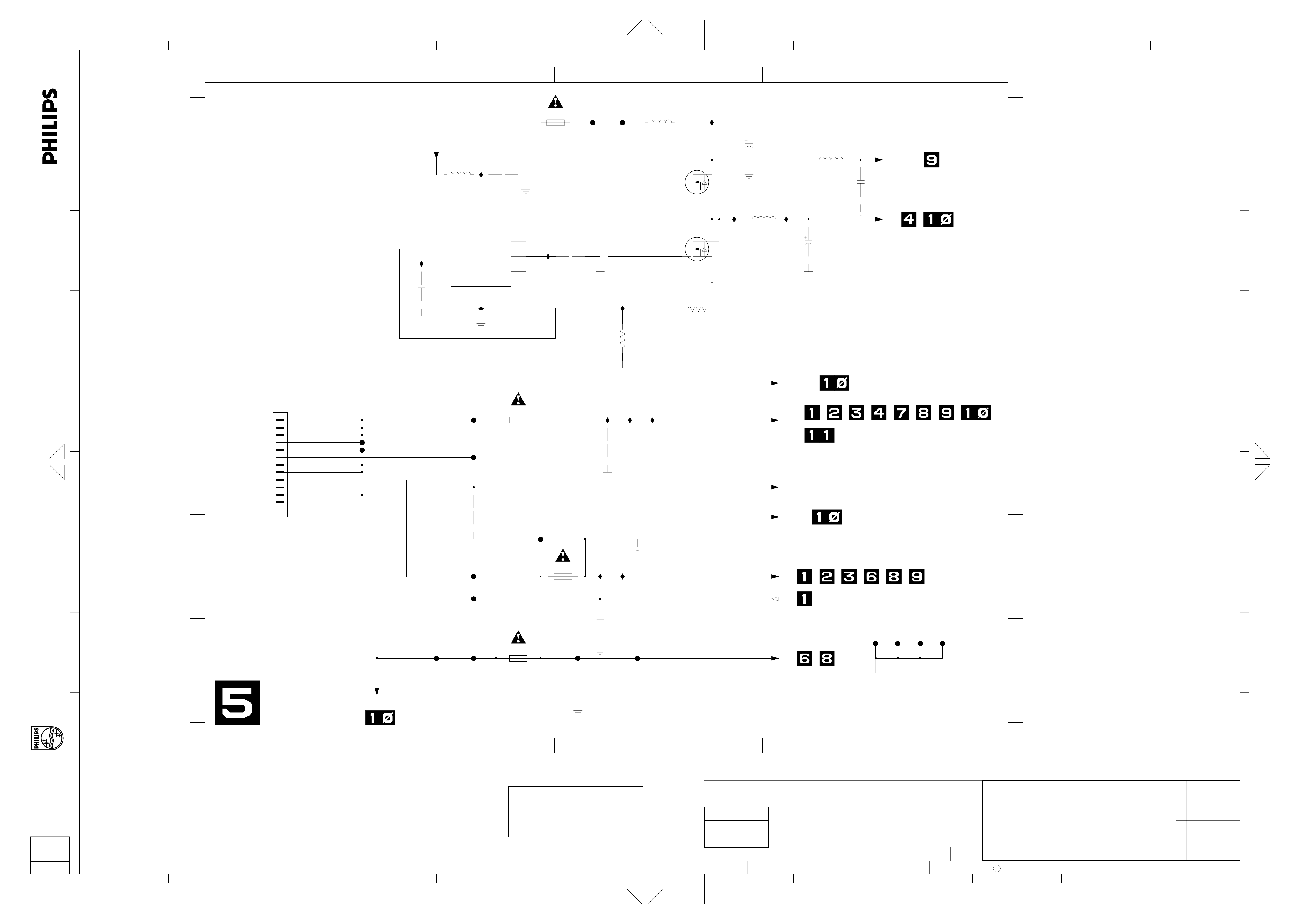
1
A
B
C
D
All rights reserved. Reproduction in whole or in parts
is prohibited without the written consent of the copyright
owner.
E
F
G
A
B
C
D
E
2
3 13
1234567
1500
1
2
3
4
5
6
7
8
9
10
11
12
B12B-PH-SM4-TBT(LF)
F1502
F1505
4
+12V
NCP1571D
I500
2515
470n
BLMP18P
7501
7
4
5502
VFB
COMP
F1501
5
I502
I501
F1506
2521
F1509
F1510
2514
100n
1
VCC
GATE-H
GATE-L
PGDELAY
PWRGD
GND
8
100n
2518
100p
1505
5
6
3
2
F1A
F502
1506
I503
1A F
2527
10n
4500
not used
1507
1A F
F500
I511
I508
2519
2524
100n
F501
I504
3503
I509
100n
I512
1%
1K5
7
5501
BLM31
I510
7500-1
STS5DNF20V
2
7500-2
STS5DNF20V
4
3504
1K5
I505
1%
78
1
56
3
I506
8
2512
6.3V
100u
5503
10u
SLF10145
I507
2516
3V3_HDMI
+3V3
+12V
+5V_HDMI
+5V
ION
9
5504
BLM18P
6.3V
100u
2517
100n
1V8_VIP
+1V8
106
11
A
1500 C1
1501 F7
1502 F7
1503 F7
1504 F7
1505 D3
1506 A4
1507 E4
1509 F3
2512 A5
2514 A3
2515 B2
2516 B6
2517 A6
2518 B3
2519 D4
2521 D3
2524 E4
2525 F4
2526 F4
2527 B4
3503 C4
B
3504 B5
4500 E4
4501 F3
5501 A5
5502 A3
5503 B6
5504 A6
7500-1 A5
7500-2 B5
7501 B3
F1501 D3
C
D
F1502 D2
F1505 D2
F1506 D3
F1509 E3
F1510 E3
F1512 F4
F1513 F2
F1514 F4
F1515 F3
F500 A4
F501 A4
F502 E3
I500 B2
I501 C3
I502 A3
I503 B3
I504 B4
I505 A5
I506 B5
I507 B6
I508 D4
I509 D4
I510 D4
I511 E4
12
A
B
C
D
E
F
E
I512 E4
G
H
gedeeltelijk, is niet toegestaan dan met schriftelijke
Alle rechten voorbehouden. Verveelvuldiging, geheel of
toestemming van de auteursrechthebbende.
I
F
1
-5V_HDMI
2525
100n
F1513
24
F1515
1509
F500mA
4501
not used
3
F1514
2526
F1512
-5V
100n
567
AV003477
1501
DVD+RWSETNAMECHN
1502
1503
1504
H
F
I
J
1
2
4
5
STAGE: LAB 1
DATE: 04-12-01
6
7
CLASS_NO
3pc332
2004-11-12
NAME
Ulreich / Linde
0
CHRY - F 05
1
2004-12-01
2004-11-050
J
3103 603 3060
2
3
83
Power Supply
SUPERS.
DATECHECK
2004-09-27
9
12
C
10 13
KONINKLIJKE PHILIPS ELECTRONICS N.V. 2000
11
130
12
5
A3
Page 25
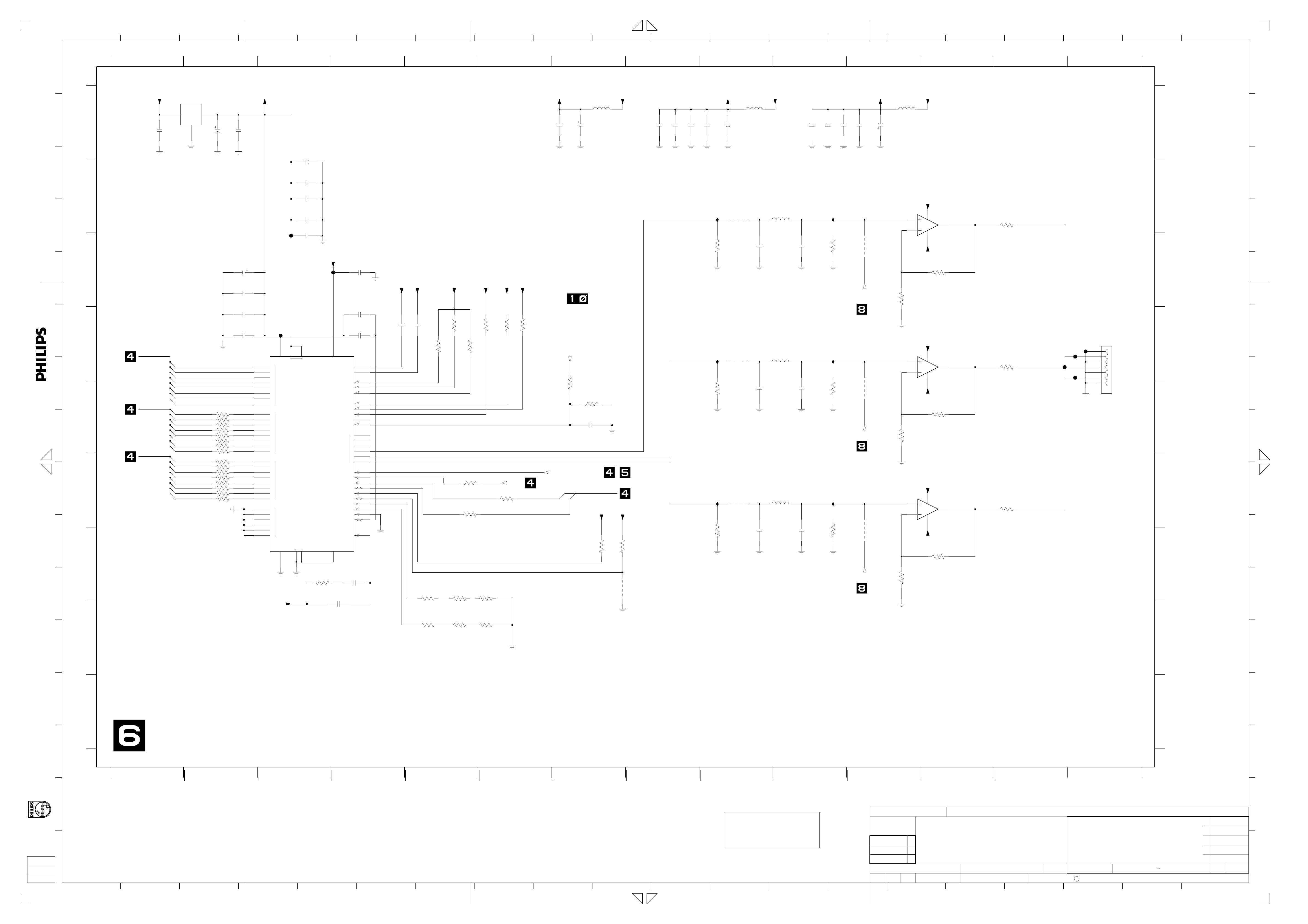
1
32
4
5
6
7
8
9
10
11
12
1413
15
16
17
18 19
20
A
B
A
C
B
D
C
E
F
D
G
E
H
I
F
J
G
K
All rights reserved. Reproduction in whole or in parts
is prohibited without the written consent of the copyright
owner.
H
L
M
I
1
+3V3
2605
ITU_OUT(7:0)
CbCr(0:7)
Y(0:7)
2
7600
LF25CDT
13
100n
OUTIN
COM
2
ITU_OUT(0)
ITU_OUT(1)
ITU_OUT(2)
ITU_OUT(3)
ITU_OUT(4)
ITU_OUT(5)
ITU_OUT(6)
ITU_OUT(7)
CbCr(0)
CbCr(1)
CbCr(2)
CbCr(3)
CbCr(4)
CbCr(5)
CbCr(6)
CbCr(7)
Y(0)
Y(1)
Y(2)
Y(3)
Y(4)
Y(5)
Y(6)
Y(7)
2606
4u7 35V
GND
10R3635
10R3636
10R3637
10R3638
10R3639
10R3640
10R3641
10R3642
10R3643
10R3644
10R3645
3647 10R
10R3646
10R3648
10R3649
10R3650
GND
2632
47u 16V
34
+2V5
100n
2610
220u 4V
2637
100n
2611
10n
2612
100n
2613
F725
10n
GND
+3V3D_VDAC
2616
F727
2618
1n0
2619
10n
2623
100n
ADV7322KST
53
54
55
58
59
60
61
62
16
17
18
26
27
28
29
30
4
5
6
7
8
921
12
13
2
3
14
15
51
52
7603
F726
0
1
2
3
4
5
6
7
0
1
2
3
4
5
6
7
0
1
2
3
4
5
6
7
0
1
2
3
4
5
AGND
+2V5
41
VAA
S
C
Y
TEST
40
GND
10
56
VDD
Φ
VIDEO
ENCODER
DGND
11
57
GND
1
VDD_IO
COMP1
COMP2
S_HSYNC
S_VSYNC
S_BLANK
P_HSYNC
P_VSYNC
P_BLANK
CLKIN_A
CLKIN_B
RTC_SCR_TR
EXT_LF
GND_IO
64
3620
680R
2631
820p
RESET
DAC
SCLK
SDA
I2C
ALSB
RSET1
RSET2
VREF
A
B
C
D
E
F
2630
3n9
2617
10n
2620
1n0
2624
100n
45
36
50
49
48
23
24
25
33
44
43
42
39
38
37
32
63
22
19
20
47
35
31
46
34
GND
GND
+2V5
2621
100n
2622
56
100n
3609
3627
1%2K7
3630
1%
2K7
10K
3606
3628
10R
3631
10R
10K
3610
3621
33R
3624
100R
+2V5+2V5+2V5
3607
10K
3629
3632
330R 1%
+2V5 +2V5
10K
3619
100R
1%330R
3633
P_CLK
GND
10K
3634
10K
+3V3D_VDAC
2600
GND
PNX7100_ITU_OUT_CLK
SCL0
SDA0
2601
100n
GND
RESET_PROGSCANn
22R
3605
7
47u 16V
3608
47K
2625
1n0
5600
BLM21
3622
GND
4K7
+3V3
+3V3D_VDAC+3V3D_VDAC
3623
GND
4600
4K7
not used
8910
2633
1n0
2634
1n0
2024
2603
100n
100n
I724
3601
I726
3612
I728
3617
+5V_PS
2604
1%
300R
1%
300R
1%
300R
5601
4u7
4u7
5604
5606
5608
2614
2626
2628
+5V
6p8
6p8
6p8
5605
2u2
5607
2u2
5609
2u2
2615
2627
2629
2635
33p
33p
33p
1n0
2636
I725
I727
I729
1n0
3602
3613
3618
2607
1%
300R
1%
300R
1%
300R
100n
2608
100n
4601
D_YUiVi
4602
4603
not used
11 12 13
-5V_PS
2609
not used
not used
5603
4u7
4u7
4
3604
3
2
3615
5
6
3626
1%1K0
1%
1K0
1K0 1%
-5V
+5V_PS
5
2
-5V_PS
+5V_PS
8
4
-5V_PS
+5V_PS
8
4
-5V_PS
7601
AD8091ART3
1
3035
1K0 1%
7602-1
AD8092AR
1
3614
1K0 1%
7602-2
AD8092AR
7
3625
1%
1K0
3037
75R 1%
3611
1%
75R
3616
75R
1%
F1604
F1601
F1602
F1606
07FMN-BMT-A-TFT
PROGSCAN
14
1002
1
2
3
4
5
6
7
GND
Y
GND
PB
GND
PR
GND
A
B
C
D
TO ANALOG BOARD
E
F
G
H
I
1002 D14
2024 A8
2600 A7
2601 A7
2603 A9
2604 A9
2605 A1
2606 A2
2607 A10
2608 A11
2609 A11
2610 A3
2611 B3
2612 B3
2613 B3
2614 C9
2615 C10
2616 C2
2617 C4
2618 C2
2619 D2
2620 D4
2621 D4
2622 D5
2623 D2
2624 D4
2625 E7
2626 E9
2627 E10
2628 G9
2629 G10
2630 G4
2631 G4
2632 A2
2633 A8
2634 A8
2635 A10
2636 A10
2637 B3
3035 C12
3037 B13
3601 C9
3602 C10
3604 C11
3605 E7
3606 D5
3607 D6
3608 E7
3609 D5
3610 D5
3611 D13
3612 E9
3613 E10
3614 E12
3615 E11
3616 F13
3617 G9
3618 G10
3619 F6
3620 G3
3621 F5
3622 G7
3623 G7
3624 F5
3625 G12
3626 G11
3627 G5
3628 G5
3629 G6
3630 H5
3631 H5
3632 H6
3633 D6
3634 D6
3635 E2
3636 E2
3637 E2
3638 E2
3639 E2
3640 E2
3641 E2
3642 E2
3643 F2
3644 F2
3645 F2
3646 F2
3647 F2
3648 F2
3649 F2
3650 F2
4600 G7
4601 C11
4602 E11
4603 G11
5600 A7
5601 A9
5603 A11
5604 B9
5605 B10
5606 D9
5607 D10
5608 F9
5609 F10
7600 A2
7601 B12
7602-1 D12
7602-2 F12
7603 D3
F1601 D14
F1602 D14
F1604 D13
F1606 D14
F725 C3
F726 D3
F727 C3
I724 B9
I725 B10
I726 D9
I727 D10
I728 F9
I729 F10
A
B
C
D
E
F
G
H
I
J
K
L
M
N
gedeeltelijk, is niet toegestaan dan met schriftelijke
Alle rechten voorbehouden. Verveelvuldiging, geheel of
toestemming van de auteursrechthebbende.
O
P
1
12
3456
5
6
I
7
8
9
7
10
8910
STAGE: LAB 1
11
CLASS_NO
3pc332
DATE: 04-12-02
2004-11-12
NAME
11
12
13
AV003477
Voko / Linde
1
2
3
CHECK
12
DVD+RWSETNAMECHN
13 14
CHRY - F 05
PROG SCAN DAC
SUPERS.
DATE
161514
2004-09-27
17
12
3103 603 3060
130
C
KONINKLIJKE PHILIPS ELECTRONICS N.V. 2004
18432
N
O
0
2004-12-01
2004-11-050
P
6
A2
2019
Page 26
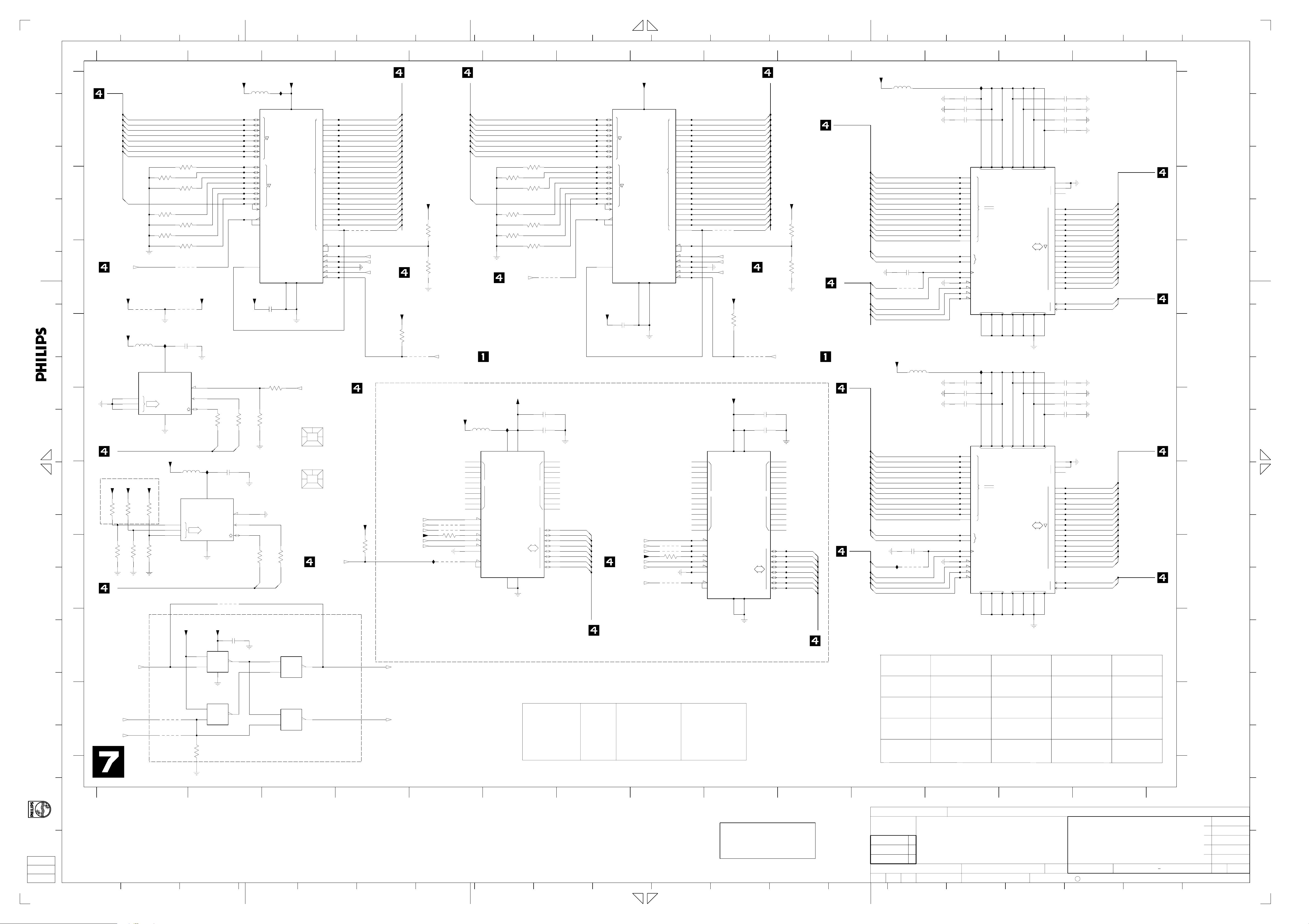
1
2
3
4
5
6
7
8
9
10
11
12
13
14
16
17
18
1915
20
A
PCI_AD(31:0)
B
A
C
B
D
XIO_ACK
E
F
C
VDD_NOR VDD_NAND
+3V3
D
M24C64-WMN6
G
1
2
3
E
H
I
F
not used
3864
10K
3866
J
10K
3865
G
K
is prohibited without the written consent of the copyright
All rights reserved. Reproduction in whole or in parts
owner.
L
H
XIO_SEL_NORFLASH
M
I
PCI_AD(23)
PCI_AD(22)
N
1
PCI_AD(24)
PCI_AD(25)
PCI_AD(26)
PCI_AD(27)
PCI_AD(28)
PCI_AD(29)
PCI_AD(30)
PCI_AD(31)
PCI_AD(0)
4802
not used
5809
BLMP18P
7810
(8Kx8)
EEPROM
0
ADR
1
2 SDA
IIC1
+3V3+3V3+3V3
10K
3868
3869
10K
10K
10K
3867
3814
10K
3812
10K
3810
10K
I801
84
Φ
+3V3
1
2
3
IIC0
4808
4809
not used
3815
10K
3813
10K
3811
10K
3809
10K
4804
not used
4803
2833
100n
WC
SCL
DEVICE
CHRY BOOT
5808
BLMP18P
7
6
5
I800
84
Φ
(8Kx8)
EEPROM
0
ADR
1
2 SDA
delete for 16MB FLASH
2
5
3801
VDD_NOR
10K
VDD_NOR
7803-1
74LVC00AD
1
7803-2
74LVC00AD
4
23
VDD_NOR
D
D
D
D
3800
2K2
22K
100R
9
10
12
13
I807
ROM
ROM
(4Mx16)
(2Mx16)
[FLASH]
[FLASH]
VDD_NOR
46
27
2746
3870
100R
SCL0
&
&
7807
AM29DL640G-70EI
7801
AM29DL324GB-70EI
37
37
0
0
1
1
2
2
3
3
4
4
5
5
6
6
7
7
8
8
9
9
A
10
A
10
11
11
12
12
13
13
14
14
15
15
16
16
17
17
18
18
19
19
20
20
21
WP
WP
ACC
ACC
CE
CE
OE
OE
BYTE
BYTE
WE
WE
RES
RES
MPIO19_EEPROM_En
0605
0609
14
8
7
14
11
7
25
24
23
22
21
20
19
18
8
7
6
5
4
3
2
1
1
48
17
16
9
10
13
14
26
28
47
11
12
SOFTWARE
SOFTWARE
XIO_ACK
for 16MB FLASH only
3807
SDA1
7809
M24C64-WMN6
DEVICE
APPLICATION
&
&
14
7
14
7
100R
2832
100n
WC
SCL
4815
3806
SCL1
2836
100n
3
6
+3V3
29
31
33
35
38
40
42
44
30
32
34
36
39
41
43
45
15
13
VDD_NOR
100R
7
6
5
5803
BLMP18P
0
0
1
1
2
2
3
3
4
4
5
5
6
6
7
7
8
8
9
9
10
10
11
11
12
12
13
13
14
14
15
15
A-1
A-1
BY
BY
RY
RY
NC
2830
100n
3803
3805
SDA0
7803-3
74LVC00AD
7803-4
74LVC00AD
456
789
10
11
12 13 14
0605 E3
0609 F3
2806 A12
VDD_NOR
7805
AM29DL640G-70EI
7811
AM29DL324GB-70EI
37
PCI_AD(31:0)
PCI_AD(1)
PCI_AD(2)
PCI_AD(3)
PCI_AD(4)
PCI_AD(5)
PCI_AD(6)
PCI_AD(7)
PCI_AD(8)
PCI_AD(9)
PCI_AD(10)
PCI_AD(11)
PCI_AD(12)
PCI_AD(13)
PCI_AD(14)
PCI_AD(15)
PCI_AD(16)
PCI_AD(17)
PCI_AD(18)
PCI_AD(19)
PCI_AD(20)
PCI_AD(21)
PCI_AD(22)
4800
3817
4K7
*
XIO_SEL_NORFLASH_L
PCI_CBE(2)
4K7
10K
3816
not used
PCI_CBE(1)
VDD_NOR
3849
PCI_AD(31:0)
PCI_AD(24)
PCI_AD(25)
PCI_AD(26)
PCI_AD(27)
PCI_AD(28)
PCI_AD(29)
PCI_AD(30)
PCI_AD(31)
PCI_AD(0)
3842
10K
3844
10K
3846
10K
XIO_ACK
3841
10K
3843
10K
3845
10K
3847
10K
4812
not used
29
29
31
31
33
33
35
35
38
38
40
40
42
42
44
44
30
30
32
32
34
34
36
36
39
39
41
41
43
43
45
45
15
15
13
VDD_NOR
0
0
1
1
2
2
3
3
D
D
4
4
5
5
6
6
7
7
8
8
9
9
10
10
11
11
D
D
12
12
13
13
14
14
15
15
A-1
A-1
BY
BY
RY
RY
NC
2834
100n
37
ROM
ROM
(4Mx16)
(2Mx16)
[FLASH]
[FLASH]
2746
2746
A
10
A
10
11
11
12
12
13
13
14
14
15
15
16
16
17
17
18
18
19
19
20
20
21
WP
WP
ACC
ACC
CE
CE
OE
OE
BYTE
BYTE
WE
WE
RES
RES
3848
PCI_AD(1)
PCI_AD(2)
PCI_AD(3)
PCI_AD(4)
PCI_AD(5)
PCI_AD(6)
PCI_AD(7)
PCI_AD(8)
PCI_AD(9)
PCI_AD(10)
PCI_AD(11)
PCI_AD(12)
PCI_AD(13)
PCI_AD(14)
PCI_AD(15)
PCI_AD(16)
PCI_AD(17)
PCI_AD(18)
PCI_AD(19)
PCI_AD(20)
PCI_AD(21)
PCI_AD(22)
10K
25
0
0
1
1
2
2
3
3
4
4
5
5
6
6
7
7
8
8
9
9
25
24
24
23
23
22
22
21
21
20
20
19
19
18
18
8
8
7
7
6
6
5
5
4
4
3
3
2
2
1
1
48
48
17
17
16
16
9
9
10
10
13
14
14
26
26
28
28
47
47
11
11
12
12
4801
*
XIO_SEL_NORFLASH_H
PCI_CBE(2)
PCI_CBE(1)
VDD_NOR
PCI_AD(31:0)
VDD_NORVDD_NOR
3819
3818
4K7
4K7
not used
SDRAM_ADDR(14:0)
SDRAM_CTRL
+3V3
5802
BLMP18P
SDRAM_ADDR(0)
SDRAM_ADDR(1)
SDRAM_ADDR(2)
SDRAM_ADDR(3)
SDRAM_ADDR(4)
SDRAM_ADDR(5)
SDRAM_ADDR(6)
SDRAM_ADDR(7)
SDRAM_ADDR(8)
SDRAM_ADDR(9)
SDRAM_ADDR(10)
SDRAM_ADDR(11)
SDRAM_ADDR(12)
SDRAM_ADDR(14)
SDRAM_ADDR(13)
not used
HSCKB
CKE
RAS(0)
CAS(0)
WE(0)
4810
I802
100n2806
2808 100n
100n2810
100n2807
100n2809
100n2811
A
100n2812
MT48LC8M16A2P
MT48LC16M16A2P
10p2814
7804
7812
23
23
24
24
25
25
26
26
29
29
30
30
31
31
32
32
33
33
34
34
22
22
35
35
36
20
20
21
21
38
38
37
37
19
19
18
18
17
17
16
16
0
0
1
1
2
2
3
3
4
4
5
5
6
6
7
7
8
8
9
9
10
10
11
11
12
0
0
1
1
CLK
CLK
CKE
CKE
CS
CS
RAS
RAS
CAS
CAS
WE
WE
BA
BA
1
1
A
A
28
28
VDD
VCC
0
0
2M-1
4M-1
VSS
VSS
14
14
41
41
27
3
9
3
Φ
Φ
9
VDDQ
VCCQ
27
DRAM
DRAM
2M X 16 X 4
4M X 16 X 4
VSSQ
VSSQ
6
6
54
54
12
12
43
43
46
46
D
D
DQM
DQM
49
49
NC
52
52
NC
10
10
11
11
12
12
13
13
14
14
15
15
SDRAM_DATA(31:0)
40
40
2
36
1
0
1
1
2
2
3
3
4
4
5
5
6
6
7
7
8
8
9
9
H
U
L
L
SDRAM_DATA(17)
4
4
SDRAM_DATA(18)
5
5
SDRAM_DATA(19)
7
7
SDRAM_DATA(20)
8
8
SDRAM_DATA(21)
10
10
SDRAM_DATA(22)
11
11
SDRAM_DATA(23)
13
13
SDRAM_DATA(24)
42
42
SDRAM_DATA(25)
44
44
SDRAM_DATA(26)
45
45
SDRAM_DATA(27)
47
47
SDRAM_DATA(28)
48
48
SDRAM_DATA(29)
50
50
SDRAM_DATA(30)
51
51
SDRAM_DATA(31)
53
53
39
39
15
15
SDRAM_CTRL
DQM(3)
DQM(2)
SDRAM_DATA(16)
2
2
0
B
C
2808 A12
2809 A13
2810 A12
2811 A13
2812 A13
2814 C11
2818 E6
2819 E6
2820 D12
2821 D13
2822 E12
2823 E13
2824 E12
2825 E13
2826 E13
2827 E9
2828 E9
2829 G11
2830 C3
2832 F2
2833 D1
2834 D7
2836 H2
3800 D3
3801 I2
3802 G8
3803 E2
3804 G5
3805 G2
3806 E2
3807 E2
3808 G4
3809 C1
3810 B1
3811 B1
3812 B1
3813 B1
3814 B1
3815 A1
3816 C5
3817 B5
3818 C10
3819 B10
2807 A13
A
B
C
D
E
F
3841 A6
3842 B6
3843 B6
3844 B6
3845 B6
3846 B6
3847 C6
3848 D9
3849 D4
3864 F1
3865 G1
3866 F1
3867 G1
3868 F1
3869 G1
3870 G3
4800 B4
4801 B9
4802 C1
4803 C1
4804 C1
4805 G8
4806 G8
4807 G8
4808 I1
4809 I1
4810 C11
4811 G11
4812 C6
4813 D5
4814 D9
4815 G2
4817 F5
4818 F5
4819 G5
5802 A11
5803 A2
5804 D11
5805 E5
5808 F2
5809 D1
7801 A3
G
H
I
J
K
XIO_SEL_NANDFLASH
+3V3
4K7
3808
4813
not used
PCI_AD(0)
PCI_AD(1)
VDD_NAND
PCI_CBE(1)
PCI_CBE(2)
PNX7100_RESETn
4817
4818
3804 4K7
I806
4819
+3V3
5805
BLMP18P
7802
TC58V64AFTI
6
7
8
9
10
13
14
15
16
17
43
2
3
5
4
42
40
41
VDD_NAND
I803
23
44
Φ
EEPROM
8-BIT SERIAL
NC NC
CE
CLE
ALE
WP
WE
RE
GND
B
R
1
D
22
2819
100n
2818
100n
1
2
3
4
5
6
7
8
28
29
30
31
32
35
36
37
38
39
PCI_AD(24)
18
PCI_AD(25)
19
PCI_AD(26)
20
PCI_AD(27)
21
PCI_AD(28)
24
PCI_AD(29)
25
PCI_AD(30)
26
PCI_AD(31)
27
XIO_SEL_NANDFLASH
PCI_AD(0)
PCI_AD(1)
VDD_NAND
PCI_CBE(1)
PCI_CBE(2)
XIO_ACK
4806
4807
4805
4K73802
7814
TC58256AFTI
7806
TC58128AFTI
1
1
2
2
3
3
4
4
5
5
10
10
11
11
14
14
15
15
20
20
21
21
22
22
23
23
24
24
9
9
16
16
17
17
19
19
18
18
8
8
6
6
7
7
NC
NC
CE
CE
CLE
CLE
ALE
ALE
WP
WP
WE
WE
RE
RE
GND
GND
BY
BY
RY
RY
4814
not used
VDD_NAND
37
12
12
37
Φ
Φ
EEPROM
EEPROM
8-BIT SERIAL
8-BIT SERIAL
13
36
13
36
2828
100n
2827
100n
D
D
PNX7100_RESETn
25
25
26
26
27
27
28
28
33
33
34
34
35
NC
NC
35
38
38
39
39
40
40
45
45
46
46
47
47
48
48
29
29
1
1
30
30
2
2
31
31
3
3
32
32
4
4
41
41
5
5
42
42
6
6
43
43
7
7
44
44
8
8
PCI_AD(24)
PCI_AD(25)
PCI_AD(26)
PCI_AD(27)
PCI_AD(28)
PCI_AD(29)
PCI_AD(30)
PCI_AD(31)
SDRAM_ADDR(14:0)
SDRAM_ADDR(0)
SDRAM_ADDR(1)
SDRAM_ADDR(2)
SDRAM_ADDR(3)
SDRAM_ADDR(4)
SDRAM_ADDR(5)
SDRAM_ADDR(6)
SDRAM_ADDR(7)
SDRAM_ADDR(8)
SDRAM_ADDR(9)
SDRAM_ADDR(10)
SDRAM_ADDR(11)
SDRAM_ADDR(12)
SDRAM_ADDR(14)
SDRAM_ADDR(13)
SDRAM_CTRL
HSCKB
CKE
RAS(0)
CAS(0)
WE(0)
+3V3
BLMP18P
2829 10p
not used
4811
I805
5804
2820 100n
2822 100n
MT48LC8M16A2P
MT48LC16M16A2P
7808
7813
23
23
24
24
25
25
26
26
29
29
30
30
31
31
32
32
33
33
34
34
22
22
35
35
36
20
20
21
21
38
38
37
37
19
19
18
18
17
17
16
16
100n2824
0
0
1
1
2
2
3
3
4
4
5
5
6
6
7
7
8
8
9
9
10
10
11
11
12
0
0
1
1
CLK
CLK
CKE
CKE
CS
CS
RAS
RAS
CAS
CAS
WE
WE
I804
1
1
A
A
BA
BA
28
28
14
27
14
27
VDD
VCC
2M X 16 X 4
4M X 16 X 4
0
0
2M-1
4M-1
VSS
VSS
41
54
41
54
3
3
Φ
Φ
DRAM
DRAM
6
6
9
9
VDDQ
VCCQ
VSSQ
VSSQ
12
12
43
43
46
46
D
D
DQM
DQM
49
49
NC
52
52
2821 100n
2825 100n
2826 100n
40
NC
40
2
36
1
2
2
0
0
4
4
1
1
5
5
2
2
7
7
3
3
8
8
4
4
10
10
5
5
11
11
6
6
13
13
7
7
42
42
8
8
44
44
9
9
45
45
10
10
47
47
11
11
48
48
12
12
50
50
13
13
51
51
14
14
53
53
15
15
39
39
H
U
15
15
L
L
100n2823
SDRAM_DATA(0)
SDRAM_DATA(1)
SDRAM_DATA(2)
SDRAM_DATA(3)
SDRAM_DATA(4)
SDRAM_DATA(5)
SDRAM_DATA(6)
SDRAM_DATA(7)
SDRAM_DATA(8)
SDRAM_DATA(9)
SDRAM_DATA(10)
SDRAM_DATA(11)
SDRAM_DATA(12)
SDRAM_DATA(13)
SDRAM_DATA(14)
SDRAM_DATA(15)
DQM(1)
DQM(0)
SDRAM_DATA(31:0)
SDRAM_CTRL
D
E
F
G
7802 E5
PCI_AD(31:0)
PCI_AD(31:0)
7803-1 H2
7803-2 I2
7803-3 H3
7803-4 I3
not used
H
7804 A12
7805 A8
L
7806 E8
7807 A3
7808 E12
XIO_SEL_NORFLASH_L
for BOARD with
SDRAM
NOR FLASH
NAND FLASH
4800, 4801
7809 F2
7810 D1
7811 A8
7812 A12
7813 E12
7814 E8
I800 F2
I801 D1
I802 A12
I803 E6
I804 D12
I805 G11
I806 G5
I807 A3
M
N
XIO_SEL_NORFLASH_H
TRUTH TABLE - NORFLASH SELECTION
XIO_SEL_NORFLASH
0
0
1
1
PCI_AD(23)
0
1
0
1
XIO_SEL_NORFLASH_L
0
1
1
1
XIO_SEL_NORFLASH_H
1
0
1
1
32 MB SDRAM
4 MB NORFLASH
64 MB SDRAM
16 MB NORFLASH
64 MB SDRAM
8 MB NORFLASH
7804, 7808
7812, 7813
7812, 7813
7801
7805, 7807
7807
not used
not used
not used
not used
4800, 4801
I
4800
Alle rechten voorbehouden. Verveelvuldiging, geheel of
toestemming van de auteursrechthebbende.
gedeeltelijk, is niet toegestaan dan met schriftelijke
O
P
1
1234
2
34
6
567
7
8
9
10
8
11
9101112
DVD+RWSETNAMECHN
2004-09-27********
STAGE: LAB 1
DATE: 04-12-01
125
13
14
CLASS_NO
3pc332
2004-11-12
NAME
AV003477
1
2
3
Stehlik / Linde
15
CHRY - F 05
FLASH, SDRAM, EEPROM
SUPERS.
DATEMGr CHECK
16
13
17
12
14
3103 603 3060
C
KONINKLIJKE PHILIPS ELECTRONICS N.V. 2000
18
19
O
0
2004-12-01
0
2004-11-05
P
7
***10 130
A2
20
Page 27
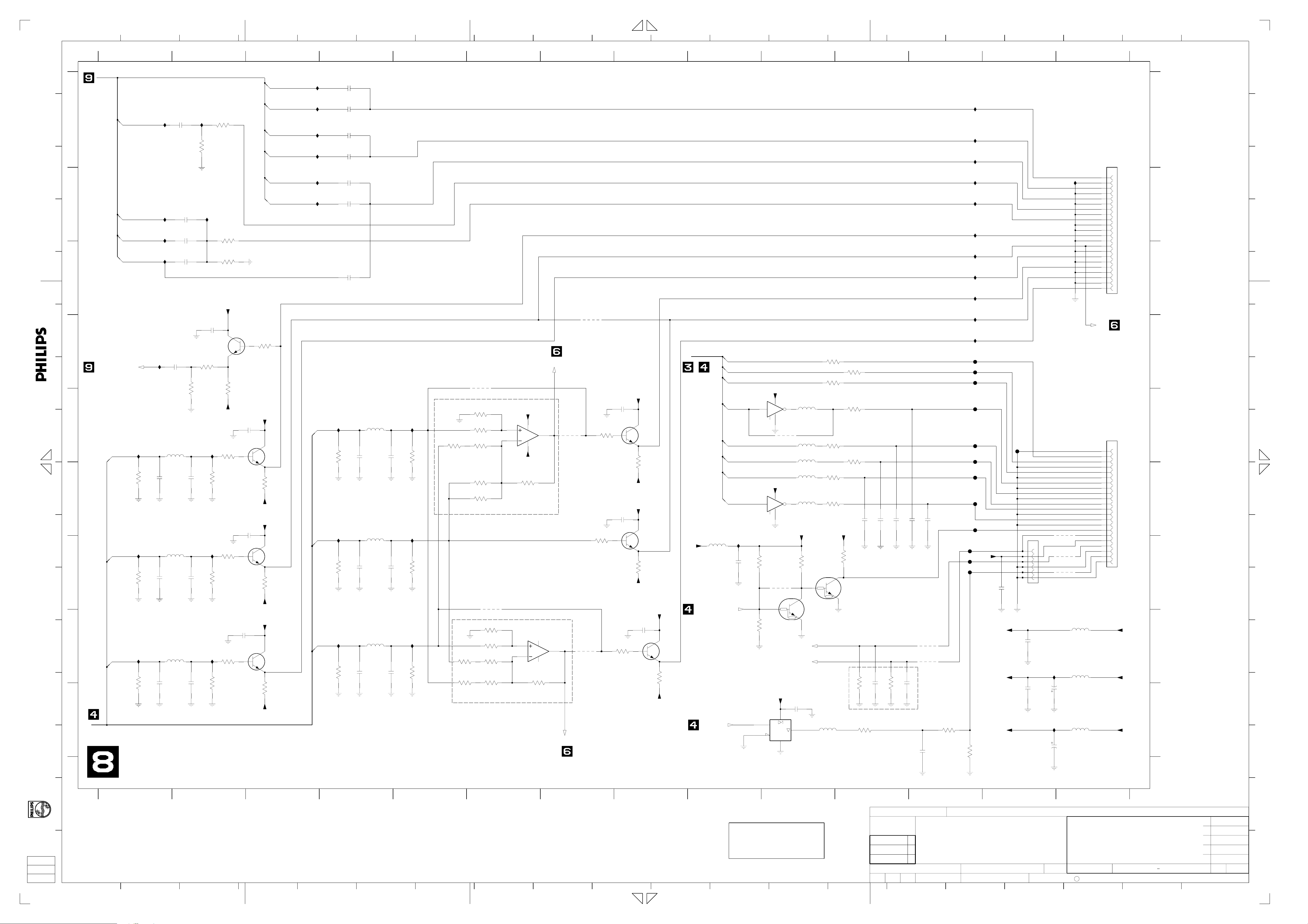
1
3
4
5
6
7 16
8
9
10
11
12
13
14
15
17
18
19
202
A
VIP_ANALOG_VIDEO_INPUT
B
A
C_IN_VIP
C
B
CVBS_Y_IN_A
D
CVBS_Y_IN_B
CVBS_Y_IN_C
E
C
F
D
CVBS_OUT_B_VIP
G
E
H
CVBS_OUT
I
F
J
Y_OUT
G
K
owner.
All rights reserved. Reproduction in whole or in parts
is prohibited without the written consent of the copyright
L
H
C_OUT
M
I
VIDEO_OUT
N
gedeeltelijk, is niet toegestaan dan met schriftelijke
toestemming van de auteursrechthebbende.
Alle rechten voorbehouden. Verveelvuldiging, geheel of
I905
3918
I906
3924
I907
3930
1%
75R
1%
75R
1%
75R
I933
2914
2926
2935
I929
I930
I931
I932
2911
22n
5908
1u5
270p
5910
1u5
270p
5912
1u5
270p
2902
47n
2907
47n
2908
47n
2909
47n
not used
3911
2915
2927
2936
I927
3902
3908
180R
1%
1%
560R
270p
270p
270p
I928
1%
560R
2938
100n
BC847B
I902
3934
I903
3936
I904
3938
3901
1%
180R
3905
180R
3906
560R
+5V_Buffer
7904
3912
-5V_Buffer
3957
100R
1%
75R
3958
100R
1%
75R
3959
100R
1%
75R
1%
1%
2K2
2933
100n
2912
100n
2924
100n
3907
100R
+5V_Buffer
7907
BC847B
3919
-5V_Buffer
+5V_Buffer
7908
BC847B
3926
-5V_Buffer
+5V_Buffer
7911
BC847B
3931
-5V_Buffer
V_IN_VIP
R_IN_VIP
U_IN_VIP
B_IN_VIP
Y_IN_VIP
G_IN_VIP
1K0
1K0
1K0
I934
I935
I936
I937
I938
I939
R_OUT
G_OUT
B_OUT
I921
3920
I923
3927
I925
3932
2900
47n
2901
47n
2903
47n
2904
47n
2905
47n
2906
47n
2941
47n
1%
75R
1%
75R
1%
75R
2916
2928
2937
5907
1u5
270p
5911
1u5
270p
5913
1u5
270p
2917
2929
2036
270p
270p
270p
I922
3935
I924
3937
I926
3939
1%
75R
1%
75R
1%
75R
3943
1%6K8
3950
3952
1%1K5
1%1K2
4904
3941
1%750R
3942
1K5
1%
3944
1%5K6
3945
4K7 1%
3947
1%4K7
not used
4905
3948
750R1%
3949
3951
3953
1%1K5
1K5 1%
1%4K7
not used
6
3
2
+5V_Buffer
7910-1
84
AD8092AR
-5V_Buffer
3946
1K0 1%
5
6
84
3954
Vi
1
7910-2
AD8092AR
7
1%1K0
78
4903
not used
DIGITAL_AUDIO
+5V_Buffer
2913
100n
4906
not used
4907
not used
Ui
3960
100R
3961
100R
2925
100n
3962
100R
7906
BC847B
3921
-5V_Buffer
+5V_Buffer
7909
BC847B
3928
-5V_Buffer
2934
100n
1K0
1K0
+5V_Buffer
3933
-5V_Buffer
7912
BC847B
1K0
+5V
MPIO7_MUTE_LVn
5901
BLMP18P
SPDIF_OUT
9
SCKE_IN
WSE_IN
SDE_IN
74LVC1G04GW
FSCLKE_IN
SCK012_OUT
WS012_OUT
SD0_OUT
74LVC1G04GW
FSCLK012_OUT
I918
2923
74HCT1G125GW
7900
7901
100n
not used
2
2
2
3940
3925
7903
1
3V3_I2S
5
NC
3
1
4911
not used
3V3_I2S
5
NC
3
1
10K
not used
4902
10K
SPDIF_OPT_IN
SPDIF_COAX_IN
VDD_125
5
EN
3
10
4
BLM18B
BLM18B
4
VDD_125
3915
2910
100n
5905
BLM18B
5906
BLM18B
5909
5914
5915
BLM18B
4K7
not used
7905
PDTC124EU
not used
4
3046
3917
3922
5904
Bead
3909
68R
3913
22R
47R
47R
68R
VDD_125
3910
68R
3914
68R
3916
47R
22K
3923
not used
7902
PDTC124EU
3903
2918 22p
3929
56R
11
2942
100K
2919 22p
22p
2920 22p
3904
not used
100K
2943
22p
2921
22p
2932
68p
2922
4900
4901
150p
for SPDIF IN only
1212345
A_VR
A_UB
A_YG
A_C
A_YCVBS
D_CVBS
D_Y
D_C
D_VR
D_YG
D_UB
A_BCLK
A_WCLK
A_DATA
A_PCMCLK
D_BCLK
D_WCLK
D_DATA0
D_PCMCLK
D_KILL
3955
1R0
I908
I910
I911
I900
I901
I912
I913
I914
I915
I916
I917
F1921
F1920
F1918
F1916
F1914
F1912
F1911
F1909
F1907
F1903
F1904
F1902
3956
+5V
DAOUT
-5V_Buffer
+5V_Buffer
100R
not used
2944
3V3_I2S
13
F1922
10n
1901
6
5
4
3
2
1
FMN-BMT
DAIO
delete for SXC
2930
100n
100n
2940
delete for DTTV
I919
2939
I920
2931
I909
4909
4908
4910
4u7
4u7
5916
5902
4u7
5903
4u7
14
1904
FMN-BMT
D_Y
1900
FMN-BMT
22
21
20
19
18
17
16
15
14
13
12
11
10
9
8
7
6
5
4
3
2
1
22
21
20
19
18
17
16
15
14
13
12
11
10
9
8
7
6
5
4
3
2
1
1900 E14
1901 F13
1904 A14
2036 H4
2900 A4
2901 A4
2902 A2
2903 A4
2904 A4
2905 B4
2906 B4
2907 B2
2908 B2
A
2909 C2
2910 I10
2911 D2
2912 E3
2913 E8
2914 F1
2915 F2
2916 E4
2917 E4
2918 F11
2919 F11
2920 F11
2921 F12
2922 F12
B
2923 G9
2924 F3
2925 F8
2926 G1
2927 G2
2928 G4
2929 G4
2930 H13
2931 I13
2932 I12
2933 H2
2934 H8
2935 H1
C
2936 H2
2937 H4
2938 D2
2939 I13
2940 I13
2941 C4
2942 H11
2943 H11
2944 G13
3046 E10
3901 A2
3902 A2
3903 H11
D
3904 H11
3905 B2
3906 C2
3907 D3
3908 D2
ANALOG BOARD INTERFACE VIDEO IN/OUT
3909 D10
3910 D11
3911 D2
3912 D2
3913 D10
3914 E11
3915 G10
3916 E11
E
3917 F10
3918 F1
3919 F3
3920 E4
3921 E8
3922 F10
3923 G11
3924 G1
3925 H9
3926 G3
3927 G4
3928 G8
3929 I11
F
3930 H1
3931 I3
5907 E4
5908 E2
5909 E10
5910 G2
5911 G4
5912 H2
5913 H4
5914 F10
5915 F10
5916 H14
7900 E9
7901 F9
7902 G11
7903 I10
7904 D2
7905 G10
7906 E8
7907 E3
7908 G3
7909 G8
7910-1 E6
7910-2 H7
7911 H3
7912 H8
F1902 G12
F1903 G12
F1904 G12
F1907 F12
F1909 F12
F1911 F12
F1912 E12
F1914 E12
F1916 E12
F1918 D12
F1920 D12
F1921 D12
F1922 E13
I900 B12
I901 B12
I902 E2
I903 G2
I904 H2
I905 E1
I906 G1
I907 H1
I908 A12
I909 B14
I910 A12
I911 A12
I912 B12
I913 C12
I914 C12
I915 C12
I916 C12
I917 D12
I918 G9
I919 H13
I920 I13
I921 E4
I922 E5
I923 F4
I924 F5
I925 H4
I926 H5
I927 A2
I928 B2
I929 A1
I930 B1
I931 B1
I932 C1
I933 D1
I934 A3
I935 A3
I936 A3
I937 A3
I938 B3
I939 B3
A
B
C
D
E
F
G
H
I
3932 H4
3933 H8
3934 F2
3935 E5
3936 G2
3937 G5
3938 H2
J
3939 H5
3940 G9
3941 E6
3942 E6
G
3943 E5
3944 E6
3945 F6
3946 F6
3947 F6
K
3948 H6
3949 H6
ANALOG BOARD INTERFACE AUDIO IN/OUT
3950 H5
3951 H6
3952 H5
+3V3
3953 H6
3954 H6
3955 I12
H
3956 I12
3957 E2
L
3958 G2
3959 H2
3960 E7
-5V
3961 G7
3962 H8
4900 H12
4901 H12
4902 G10
4903 D7
M
4904 D6
4905 G6
I
+5V
4906 E7
4907 H7
4908 G14
4909 F14
4910 G14
4911 E10
5901 G9
N
5902 H14
5903 I14
5904 I10
5905 E10
5906 E10
O
P
1
1234
2
3
4
5
6
567
7
8
911
8 9 10 11
STAGE: LAB 1
DATE: 04-12-01
NAME
12
14
12
CHN SETNAME DVD+RW
CLASS_NO
3pc332
2004-11-12
AV003477
1
2
3
Kabinger / Linde
1513
CHECK
CHRY - F 05
Video IO
SUPERS.
DATE
2004-09-27
16
13 14
12
C
KONINKLIJKE PHILIPS ELECTRONICS N.V. 2000
1710
18
3103 603 3060
8
130
19
0
2004-12-01
0 2004-11-05
A2
20
O
P
Page 28
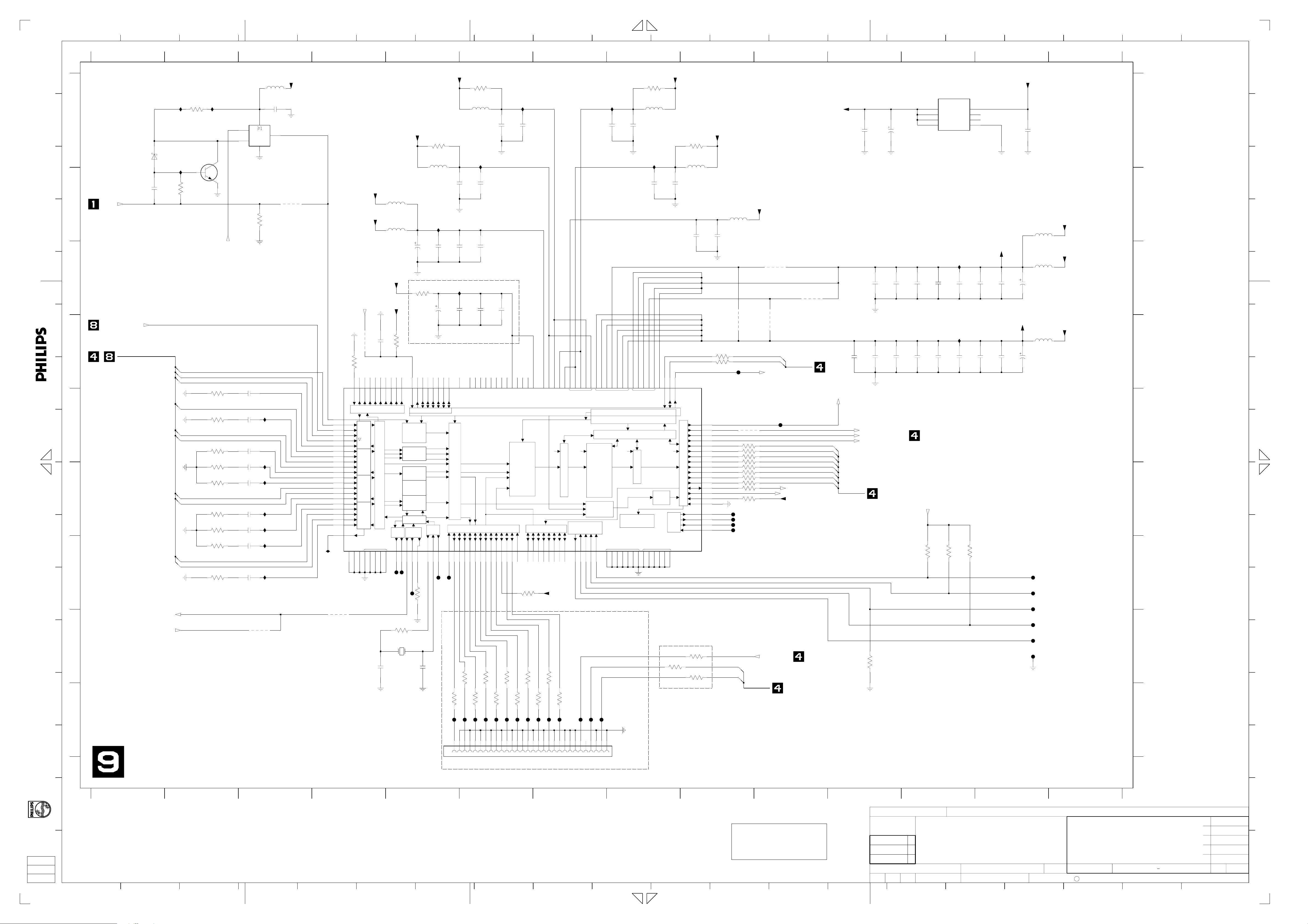
2
3
4
5
6
7
9
10
11
12
13
14
15
16
17
18
19
2081
1
A
B
A
C
B
VIP_FB
D
E
C
CVBS_OUT_B_VIP
F
D
VIP_ANALOG_VIDEO_INPUT
G
E
H
I
F
J
G
K
owner.
All rights reserved. Reproduction in whole or in parts
is prohibited without the written consent of the copyright
L
H
M
I
N
gedeeltelijk, is niet toegestaan dan met schriftelijke
toestemming van de auteursrechthebbende.
Alle rechten voorbehouden. Verveelvuldiging, geheel of
6000
1PS76SB10
150p
2019
MPIO5_VIP_ERROR
VIP_INTA
I010
3005
680R
I012
3007
680R
BC847B
CVBS_Y_IN_A
CVBS_Y_IN_B
CVBS_Y_IN_C
C_IN_VIP
G_IN_VIP
Y_IN_VIP
B_IN_VIP
U_IN_VIP
R_IN_VIP
V_IN_VIP
2345678
I002
2022
M5
TEXT
VSSI
F11
10n
M9
FIFO
J11L5L9
not used
+3V3_VIP
2026
P9INT_A
N9SCL
P10SDA
AUDIO
3008
22R
+3V3_VIP
3022
100R
not used
5008
BLM18P
100n
10n
2020
3087 100R
3088 100R
7007
SAA7118E
SAA7117AE
for XXXX only
K13IGP1
L14IGP0
K14IGPV
K12IGPH
G14IDP0
G12IDP1
H11IDP2
H14IDP3
H13IDP4
J14IDP5
J13IDP6
K11IDP7
M14ICLK
L13IDQ
OUTPUT FORMATTER I-PORT
CLK
N12ITRDY
L12ITRI
N11ASCLK
P12ALRCLK
P11AMCLK
M12AMXCLK
3099
22R
3015
22R
I011
74LVC1G32GW
7003
3032
1R0
56R for SAA7117
3031
1R0
56R for SAA7117
3030
1R0
56R for SAA7117
3029
1R0
56R for SAA7117
3028
1R0
56R for SAA7117
3027
1R0
56R for SAA7117
3026
1R0
56R for SAA7117
3025
1R0
56R for SAA7117
3024
1R0
56R for SAA7117
1
2
VIP_IGP1
5001
BLMP18P
2014
7002
2040
47n
2039
47n
2038
47n
2037
47n
2035
47n
2033
47n
2032
47n
2031
47n
2030
47n
not used
100n
35
1K0
3021
I014
I016
I017
I018
I019
I020
I021
4008
+3V3_VIP
4
4000
not used
I001
3086
M13 FSW
J2 A|11
K1 A|12
K2 A|13
L3 A|14
K3 A|1D
G4 A|21
G3 A|22
H2 A|23
J3 A|24
H1 A|2D
E3 A|31
F2 A|32
F3 A|33
G1 A|34
F1 A|3D
B1 A|41
D2 A|42
D1 A|43
E1 A|44
D3 A|4D
M1 AOUT
AGNDL2AGNDA
C2
4007
4001
2K2
P8ADP1
N6CLKEXT
N8ADP0
AD-PORT
ANALOG1
ANALOG1
ANALOG1
ANALOG1
VXSS
A4
M2J4H3E4C1
+3V3_VIP
1V8_VIP
+3V3_VIP
VIP_RESETn
not used
M7ADP2
VDDE_7118
2027
L7ADP3
P7ADP4
N7ADP5
BLM18P
5020
not used
5021
BLM18P
1V8_VIP
1n0
3023
L6ADP6
M6ADP7
4K7
P6ADP8
2023
N4CE
FAST
SWITCH
B
DELAY
COMP
PROC
CHROM
+ ADC1
+ ADC1
R
G
C
PROC
COMB
FIL
+ ADC1
+ ADC1
VSSA
Y
S
ANALOG INPUT CONTROL
LUM
PROC
S
SYNC
2096
VIDEO
F008
CX-8045G
33p
CLK
P4 LLC
N5 LLC2
F009
3052
1R0
1001
24M576
GPO
M10 RST0
N10 RST1
F012
4u7
3000
22R
P5RESON
P13TEST0
D13TEST1
CONTROL
RAW
A3 XTAL
L10 RTCO
4K7
3043
VIP_RTS1
2097
3049
100R
not used
5016
BLM18P
I008
2100
2018
A13TEST3
C14TEST2
Y
CB
CR
CB
CR
Y
S
XTAL
A2 XTOUT
B4 XTALI
33p
+3V3_VIP
3091
100R
not used
5010
BLM18P
2044
I009
10n
2048
100n
2049
100n
4u7
B12TEST4
A12TEST5
10n
2099
I003
2017
100n
for SAA7117 only
B2
P3
RES1
EXMCLR
2098
2016
B14
B13
RES3C3RES4C4RES5
RES2
YCBCR
YCBCR
1n0
10n
S
2015
C12
RES6
YCBCRS
C13
DECODER OUTPUT CONTROL
B10 XPD5
A11 XPD6
A6 XRDY
F001
A8 XPD0
F002
DD_IN1
DD_IN0
3014
F0330
B8 XPD1
A9 XPD2
DD_IN2
3020
22R
F0328
29330
B9 XPD3
DD_IN3
22R
3013
F0326
27
28
A10 XPD4
DD_IN5
DD_IN4
3019
22R
F0324
25
26
C11 XPD7
DD_IN7
DD_IN6
22R
3012
F0322
24
23
A7 XCLK
B7 XDQ
DD_IN_CLK
22
I005
2043
N3
N13
RES10
10n
N14
RES11
RES12P2RES13
B3
VXDD
100n
1n0
RES7N1RES8N2RES9
IIC REGISTER MAP
PRESCALER
BCS-SCALER
FIR-PREFILTER
RAW
CBCR
H-PORTX-PORT
B11 XTRI
C7 XRH
3018
22R
F0320
21
D8 XRV
22R
3011
F0318
19220
18
D14 HPD0
3034
10K
3017
22R
F0316
16
17
E11 HPD1
E13 HPD2
22R
3010
F0314
15
E12 HPD3
14
3016
22R
F0312
13
J1
L1
E2
G2
VDDA2A
VDDA3A
VDDA4A
CBCR
E14 HPD4
F13 HPD5
F14 HPD6
G13 HPD7
VDDE_7118
DD_IN_VS
DD_IN_HS
22R
3009
F0310
10
11
12
I004
2028
F4
K4
M3
VDDA
VDDA1A
H4
C5
C9
D4
D12
VDDE VDDI
1ST TASK IIC REG MAP SCALER
2ST TASK IIC REG MAP SCALER
SCALER EVENT CONTROLLER
HORIZONTAL FINE-
LINE FIFO BUFFER
(PHASE-) SCALING
VERTICAL SCALING
VBI DATA
SLICER
BOUNDARY
SCAN
D5D9D11
D6 TMS
C6 TRSTN
B6 TCK
B5 TDI
A5 TDO
for DTTV only
22R
F020
F019
F021
4
5
6
7
8
9
1
30FLZ-SM2-TB(LF)(SN)
10n
M4
M8
H12
M11
VIDEO/TEXT
ARBITER
VSSE
L4L8L11D7D10
G11
1003
100n
2029
C8
F12
C10
VIDEO FIFO
3033
100R
not used
5009
BLM18P
J12
910
+3V3_VIP
+3V3_VIP
5005
BLM18P
100n
2021
4004
for SAA7117 only
4005
delete for SAA7117
4002
delete for SAA7117
F003
4006
3048-1 47R
3048-4 47R
3047-1 47R
3047-2
3047-3 47R
3089
F004
F005
F006
F007
SDA0
SCL0
4003
for SAA7117 only
SDA0
SCL0
VIP_INTA
F011
47R3048-2
47R3048-3
47R
47R3047-4
22R3090
4K7
RESET_DTTMn
IIC0
IIC0
ITU_IN(0)
ITU_IN(1)
ITU_IN(2)
ITU_IN(3)
ITU_IN(4)
ITU_IN(5)
ITU_IN(6)
ITU_IN(7)
PNX7100_ITU_IN_CLK
PNX7100_ITU_IN_VAL
VDDI_7118
2061
VIP_IGP1
ITU_IN(7:0)
11 12
2
3
6
VOUT
7
VOUT
2045
100n
2050
10n
2063
PNX7100_ITU_IN_FID
PNX7100_VS_IN
PNX7100_HS_IN
10K
3004
2042
10n
100n
2052
2064
47u
100n
100n
2053
2065
+3V3_VIP
100n
100n
3002
2054
2066
10K
7006
LD1117D33
GND
I007
100n
2056
I006
100n
2071
10K
3006
NCVOUT
NC
INVOUT
100n
100n
3001
4
5
8
1
VDDI_7118
2058
100n
100n
2073
10K
JTAG_VIP_TMS
JTAG_VIP_TCK
JTAG_VIP_TRSTn
JTAG_VIP_TDI
JTAG_VIP_TDO
13 14
+5V
100n
2041
1V8_VIP
+3V3_VIP
+3V3_VIP
2059
2094
2060
100n
VDDE_7118
2095
100n
BLM18P
5017
for SAA7117 only
BLM18P
5018
delete for SAA7117
4u7
5019
BLM18P
4u7
F017
F018
F013
F016
F015
F014
A
B
C
D
E
F
G
H
I
1001 H5
1003 I8
2014 A3
2015 C6
2016 C6
2017 C5
2018 C5
2019 B1
2020 B9
2021 B9
2022 B8
2023 C5
2026 B8
2027 D4
2028 A8
2029 A8
2030 G3
2031 G3
2032 F3
2033 F3
2035 F3
2037 E3
2038 E3
2039 E3
2040 E3
2041 A13
2042 A11
2043 A6
2044 A6
2045 A11
2048 B6
2049 B5
2050 C11
2052 C11
2053 C12
2054 C12
2056 C12
2058 C13
2059 C13
2060 C13
2061 D11
2063 D11
2064 D11
2065 D12
2066 D12
2071 D12
2073 D13
2094 D13
2095 D13
2096 H4
2097 H5
2098 C6
2099 C5
2100 C5
3000 C5
3001 G12
3002 G12
3004 H11
3005 A2
3006 G12
3007 B2
3008 H8
3009 I7
3010 I7
3011 I6
3012 I6
3013 I6
3014 I5
3015 H9
3016 H7
3017 H6
3018 H6
3019 H6
3020 H6
3021 B2
3022 A9
3023 D5
3024 G2
3025 G2
3026 F2
3027 F2
3028 F2
3029 E2
3030 E2
3031 E2
3032 D2
3033 A8
3034 G7
3043 G5
3047-1 F9
3047-2 F9
3047-3 F9
3047-4 F9
3048-1 E9
3048-2 E9
3048-3 E9
3048-4 E9
3049 A5
3052 H5
3086 D4
3087 D9
3088 D9
3089 F9
3090 F9
3091 A6
3099 H9
4000 B3
4001 D4
4002 D9
4003 D10
4004 C10
4005 C10
4006 E9
4007 H4
4008 H3
5001 A3
5005 B9
5008 A9
5009 A8
5010 A6
5016 A5
5017 B13
5018 C13
5019 D13
5020 B5
5021 B5
6000 A1
7002 A2
7003 B2
7006 A12
7007 D9
F001 G5
F002 G5
F003 D9
F004 F9
F005 F9
F006 F9
F007 F9
F008 G5
F009 G5
F011 E10
F012 G5
F013 G13
F014 H13
F015 H13
F016 H13
F017 G13
F018 G13
F019 I7
F020 I7
F021 I7
F0310 I7
F0312 I7
F0314 I7
F0316 I6
F0318 I6
F0320 I6
F0322 I6
F0324 I6
F0326 I6
F0328 I6
F0330 I5
I001 G4
I002 A8
I003 C6
I004 A8
I005 A6
I006 D12
I007 C12
I008 B5
I009 A6
I010 A2
I011 A2
I012 A2
I014 E3
I016 E3
I017 F3
I018 F3
I019 F3
I020 G3
I021 G3
A
B
C
D
E
F
G
H
I
J
K
L
M
N
O
P
1
12345
23
46
7
67
8
91011
STAGE: LAB 1
DATE: 04-12-01
8 14
105
11
12
139
12 13
CHN SETNAME DVD+RW
CLASS_NO
3pc332
2004-11-12
NAME
AV003477
Voko / Linde
1
2
3
CHECKMGr DATE
******** 2004-09-27
15
CHRY - F 05
VIP
SUPERS.
16
17
12
14
3103 603 3060
13010 ***
C
KONINKLIJKE PHILIPS ELECTRONICS N.V. 2000
18
19
O
0
2004-12-01
0 2004-11-05
P
9
A2
20
Page 29
12345
6
A
1004 A4
2750 D3
2751 D1
2752 D1
2753 D1
2754 D2
3750 A3
3751 A3
3752 A3
3753 B2
B
C
A
D
B
owner.
All rights reserved. Reproduction in whole or in parts
is prohibited without the written consent of the copyright
E
C
F
D
+12V
G
2751
3754 C3
3755 C2
3756 C2
3757 C3 F0423 B3
3758 C2
1
ITU_OUT(0:7)
ITU_OUT(0)
ITU_OUT(1)
ITU_OUT(2)
ITU_OUT(3)
ITU_OUT(4)
ITU_OUT(5)
ITU_OUT(6)
ITU_OUT(7)
FSCLK012_OUT
SCK012_OUT
MPIO12_HDMI_IRQ
MPIO11_HDMI_RESETn
RESET_PROGSCANn
+5V_HDMI -5V_HDMI 3V3_HDMI
2753
100n
2752
100n
100n
3759 C3
3760 C3
F0403 C3
F0405 C3
F0409 C3
F0411 C3
F0413 C3
F0415 C3
F0417 B3
2
SDA0
SCL0
PNX7100_ITU_OUT_CLK
SD0_OUT
DAOUT
WS012_OUT
2754
100n
3753
22R
3755
22R
3756
22R
3758
22R
F0418 B3
F0419 B3
F0421 B3
F0424 B3F0407 C3
3750
22R
3752
22R
+5V_HDMI
3V3_HDMI
-5V_HDMI
3754
22R
3760
22R
not used
3757
22R
3759
22R
F0425 B3
F0426 B3
F0427 B3
F0428 B3
F0429 B3
F0431 A3
F0433 A3
F0435 A3
F0437 A3
F0439 A3
F0440 A4
34
1004
40
39
38
37
36
35
34
33
32
31
30
29
28
27
26
25
24
23
22
21
20
19
18
17
16
15
14
13
12
11
10
9
8
7
6
5
4
3
2
1
40FLT-SM1-TB
A
B
C
3751
22R
+12V
2750
F0439
F0437
F0435
F0433
F0431
F0429
F0428
F0427
F0426
F0425
F0424
F0423
F0421
F0419
F0418
F0417
F0415
F0413
F0411
100p
F0440
U4
U3
U2
U1
D
A
B
C
D
E
F
G
toestemming van de auteursrechthebbende.
gedeeltelijk, is niet toegestaan dan met schriftelijke
Alle rechten voorbehouden. Verveelvuldiging, geheel of
H
1
I
AV003477
CLASS_NO
3pc332
J
2004-11-12
NAME
1
2
3
Voko / Linde
123 5
2
DVD+RWSETNAMECHN
CHRY - F 05
HDMI INTERFACE
SUPERS.
2004-09-27
DATECHECK
for HDMI only
34
H
STAGE: LAB 1
DATE: 04-12-01
2004-12-01
0
2004-11-050
3103 603 3060
10
12
C
KONINKLIJKE PHILIPS ELECTRONICS N.V. 2004
4
130
6
I
J
A4
Page 30
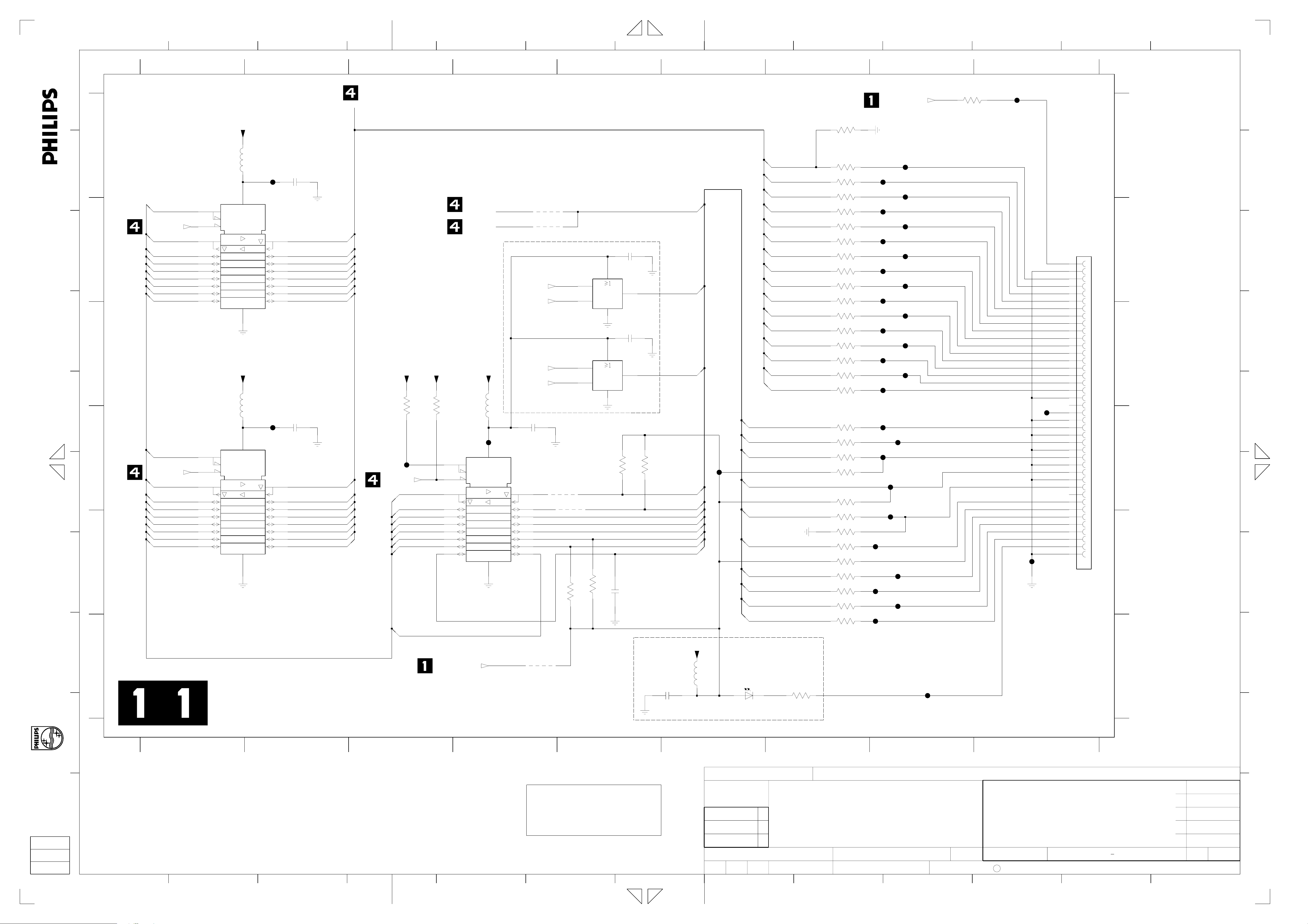
12
3
4
6
7
8
9
10
12115
13
A
A
A
B
74LVC245APW
PCI_AD(8)
XIO_SEL2
PCI_AD(24)
B
C
B
PCI_AD(30)
PCI_AD(29)
PCI_AD(28)
PCI_AD(27)
PCI_AD(26)
PCI_AD(25)
PCI_AD(31)
D
C
C
All rights reserved. Reproduction in whole or in parts
is prohibited without the written consent of the copyright
owner.
E
PCI_AD(8)
D
D
XIO_SEL2
PCI_AD(16)
F
E
E
PCI_AD(22)
PCI_AD(21)
PCI_AD(20)
PCI_AD(19)
PCI_AD(18)
PCI_AD(17)
PCI_AD(23)
G
PCI_AD(31:0)
H
F
F
gedeeltelijk, is niet toegestaan dan met schriftelijke
Alle rechten voorbehouden. Verveelvuldiging, geheel of
toestemming van de auteursrechthebbende.
I
1 2 3 4 5 6 7
12
IDE_DD(15:0)
7320
1
19
2
3
4
5
6
7
8
9
1
19
2
3
4
5
6
7
8
9
3EN1
3EN2
G3
2
3EN1
3EN2
G3
2
+3V3
5320
BLMP18P
20
1
10
+3V3
5321
BLMP18P
7321
74LVC245APW
20
1
10
F320
F321
18
17
16
15
14
13
12
11
18
17
16
15
14
13
12
11
2320
100n
IDE2_DD(8)
IDE2_DD(14)
IDE2_DD(13)
IDE2_DD(12)
IDE2_DD(11)
IDE2_DD(10)
IDE2_DD(9)
IDE2_DD(15)
2321
100n
IDE2_DD(0)
IDE2_DD(6)
IDE2_DD(5)
IDE2_DD(4)
IDE2_DD(3)
IDE2_DD(2)
IDE2_DD(1)
IDE2_DD(7)
34567
IDE2_DD(7)
IDE2_DD(8)
IDE2_DD(6)
+3V3
3339
F323
XIO_SEL2
PCI_AD(15)
PCI_AD(14)
PCI_AD(13)
PCI_AD(12)
PCI_AD(11)
PCI_AD(9)
PCI_AD(10)
PCI_AD(0)
4K7
+3V3
10K
3352
1
19
2
3
4
5
6
7
8
9
RESET_IDE2n
MPIO4_IDE2_IRQ
PCI_GNTB
+3V3
5322
BLMP18P
7322
F322
74LVC245APW
20
3EN1
3EN2
G3
1
2
10
XIO_SEL2
PCI_AD(15)
XIO_SEL2
PCI_AD(14)
2322
100n
18
17
16
15
14
13
12
11
4324
4320
4321
not used
74LVC1G32GW
74LVC1G32GW
not used
4322
4323
3356
7323
1
2
7324
1
2
47K
3353
2325
100n
5
4
3
2326
100n
4
35
470R
10p
not used
3341
3340
47K
2324
IDE2_CS1n
IDE2_CS0n
470R
IDE2_CS1n
IDE2_CS0n
IDE2_DIORn
IDE2_DIOWn
IDE2_IORDY
2323
100n
IDE2_IRQ
IDE2_DA2
IDE2_DA1
IDE2_DA0
+3V3
5323
F324
BLMP18P
IDE2_DIOWn
IDE2_DIORn
IDE2_IORDY
IDE2_DMACKn
IDE2_IRQ
IDE2_DA1
IDE2_DA0
IDE2_DA2
IDE2_CS0n
IDE2_CS1n
6320
TLMH3100
IDE2_DD(9)
IDE2_DD(5)
IDE2_DD(10)
IDE2_DD(4)
IDE2_DD(11)
IDE2_DD(3)
IDE2_DD(12)
IDE2_DD(2)
IDE2_DD(13)
IDE2_DD(1)
IDE2_DD(14)
IDE2_DD(0)
IDE2_DD(15)
not used
3358
220R
for IDE_2 only
3359
10K
3321 33R
3322
3324 33R
3326 33R
3327 33R
3330 33R
3331 33R
3333 33R
3336 33R
3342 22R
3343 82R
3344
3346
3348
3345
not used
3350 33R
3355 33R
33R
33R3323
33R3325
33R3328
33R3329
33R3332
33R3334
33R3335
22R3338
4K7
47K
82R3347
10K
33R3349
4K7
33R3351
33R3354
F0104
F0106
F0108
F0110
F0112
F0114
F0116
F0118
F0123
F0127
F0133
F0136
F0138
RESET_IDE2n
F0103
F0105
F0107
F0109
F0111
F0113
F0115
F0117
F0125
F0129
F0131
F0135
F0137
8 9
89
3320
33R
F0101
A
A
IDE2
B
B
C
C
D
D
E
E
F
F
F0139
1101
F0121
F0102
40FLZ-RSM2-R-TB(LF)(SN)
1
2
3
4
5
6
7
8
9
10
11
12
13
14
15
16
17
18
19
20
21
22
23
24
25
26
27
28
29
30
31
32
33
34
35
36
37
38
39
40
1101 B9
1101 B9
2320 A2
2320 A2
2321 D2
2321 D2
2322 D4
2322 D4
2323 F6
2323 F6
2324 E5
2324 E5
2325 B5
2325 B5
2326 C5
2326 C5
3320 A8
3320 A8
3321 A7
3321 A7
3322 A7
3322 A7
3323 A7
3323 A7
3324 B7
3324 B7
3325 B7
3325 B7
3326 B7
3326 B7
3327 B7
3327 B7
3328 B7
3328 B7
3329 B7
3329 B7
3330 B7
3330 B7
3331 C7
3331 C7
3332 C7
3332 C7
3333 C7
3333 C7
3334 C7
3334 C7
3335 C7
3335 C7
3336 C7
3336 C7
3338 D7
3338 D7
3339 D3
3339 D3
3340 D5
3340 D5
3341 D5
3341 D5
3342 D7
3342 D7
3343 D7
3343 D7
3344 D7
3344 D7
3345 E7
3345 E7
3346 D7
3346 D7
3347 E7
3347 E7
3348 E7
3348 E7
3349 E7
3349 E7
3350 E7
3350 E7
3351 E7
3351 E7
3352 D3
3352 D3
3353 E5
3353 E5
3354 E7
3354 E7
3355 F7
3355 F7
3356 E5
3356 E5
3358 F7
3358 F7
3359 A7
3359 A7
4320 B4
4320 B4
4321 B4
4321 B4
4322 D5
4322 D5
4323 D5
4323 D5
4324 F4
4324 F4
5320 A1
5320 A1
5321 C1
5321 C1
5322 C4
5322 C4
5323 F6
5323 F6
6320 F6
6320 F6
7320 A1
7320 A1
7321 D2
7321 D2
7322 D4
7322 D4
7323 B5
7323 B5
7324 C5
7324 C5
F0101 A9
F0101 A9
F0102 E9
F0102 E9
F0103 A8
F0103 A8
F0104 A8
F0104 A8
F0105 A8
F0105 A8
F0106 B8
F0106 B8
F0107 B8
F0107 B8
F0108 B8
F0108 B8
F0109 B8
F0109 B8
F0110 B8
F0110 B8
F0111 B8
F0111 B8
F0112 B8
F0112 B8
F0113 C8
F0113 C8
F0114 C8
F0114 C8
F0115 C8
F0115 C8
F0116 C8
F0116 C8
F0117 C8
F0117 C8
F0118 C8
F0118 C8
F0121 D9
F0121 D9
F0123 D8
F0123 D8
F0125 D8
F0125 D8
F0127 D8
F0127 D8
F0129 D8
F0129 D8
F0131 E8
F0131 E8
F0133 E8
F0133 E8
F0135 E8
F0135 E8
F0136 E8
F0136 E8
F0137 E8
F0137 E8
F0138 F8
F0138 F8
F0139 F8
F0139 F8
F320 A2
F320 A2
F321 D2
F321 D2
F322 D4
F322 D4
F323 D3
F323 D3
F324 D6
F324 D6
A
B
C
D
E
F
G
H
I
J
1
1 2 3 4 5 6
123456
AV003477
CLASS_NO
3pc332
STAGE: LAB 1
1
2
3
4
DATE: 04-12-01
7
2004-11-12
NAME
Ulreich / Linde
2
3
8
7
7 8 9
DVD+RWSETNAMECHN
89
CHRY - F 05
IDE 2
SUPERS.
DATECHECK
96
2004-09-27
10
12
C
KONINKLIJKE PHILIPS ELECTRONICS N.V. 2000
115
3103 603 3060
130
11
12
0
2004-12-01
2004-11-050
J
A3
13
Page 31

1300 A2 1301 A3
3
54
612
A
123
B
A
C
B
D
is prohibited without the written consent of the copyright
owner.
E
C
F
D
G
1300
1
2
3
4
5
6
7
8
9
10
11
12
13
14
15
16
17
18
19
20
21
22
23
24
25
26
27
28
29
30
31
32
33
34
35
36
37
38
39
40
56604
1301
41 42
40
39
38
37
36
35
34
33
32
31
30
29
28
27
26
25
24
23
22
21
20
19
18
17
16
15
14
13
12
11
10
9
8
7
6
5
4
3
2
1
40FLZ-RSM2-R-TB(LF)(SN)
for HDRW720 only (not used)
4
A
B
A
C
B
D
E
C
F
D
G
Alle rechten voorbehouden. Verveelvuldiging, geheel of All rights reserved. Reproduction in whole or in parts
gedeeltelijk, is niet toegestaan dan met schriftelijke
toestemming van de auteursrechthebbende.
E
H
I
AV003477
CLASS_NO
3pc332
J
2004-11-12
NAME
1
2
3
Cyniburk/Linde
1
1
CHRY - F 05
IDE Interface
SUPERS.
DATECHECK
2
DVD+RWSETNAMECHN
2004-09-27
E
H
STAGE: LAB 1
DATE: 04-12-01
I
234
2004-12-01
0
2004-11-050
3103 603 3060
12
12
C
KONINKLIJKE PHILIPS ELECTRONICS N.V. 2000
36
4
130
5
J
A4
Page 32

Page 33

Page 34

1
1234567891011121314
A
MOJO
A
B
C
B
D
E
C
F
D
G
E
H
I
F
J
G
K
is prohibited without the written consent of the copyright
All rights reserved. Reproduction in whole or in parts
owner.
H
L
M
I
N
Alle rechten voorbehouden. Verveelvuldiging, geheel of
gedeeltelijk, is niet toegestaan dan met schriftelijke
toestemming van de auteursrechthebbende.
O
P
I2C_LOCAL_SCL
I2C_LOCAL_SDA
I2C_DB_SCL
I2C_DB_SDA
JTAG_TRST
10046_TDI
10046_TDO
JTAG_TCK
JTAG_TMS
MIU_WEN
NOR_RYBY
12
10K
3118
F139
F140
F164
F165
F166
3144
F138
3147 100R
F141
100R
F142
100R
3166
3167
3119
4103
4106
4104
4105
4108
4111
{TS_DATA(0:7),TS_CLK,TS_SYNC,TS_VALID}
SPDIF
3151
3152
OPTION
+3V3_MOJO
2
3
+3V3
10K
10K
10K
10K
OPTION
3120
3117
3116
OPTION
TS_DATA(0)
TS_DATA(1)
TS_DATA(2)
TS_DATA(3)
TS_DATA(4)
TS_DATA(5)
TS_DATA(6)
TS_DATA(7)
202
SD_OUT
203
SCK_OUT
204
WS_OUT
206
SPDIF
22R
205 165
FSCLK
100R3149
6
7
8
9
36
3K3
3K3
198
39
10K
10K
3157
3156
3
10K
3114
1K0
3115
20
21
22
23
24
25
26
27
PNX8316HS
(I2C-USB-SCO)
SCL0
SDA0
SCL1
SDA1
SC0_DA
USB_OVRCUR
SC0_OFF
1104
FTR
7100-3
(AV)
4
2
1
F108
F107
0
1
2
3
TS_DATA
4
5
6
7
7100-6
PNX8316HS
41
5
OPTION
F102
10
34
56
78
9
11 12
13 14
15 16
F110
F112
F113
F111
F109
7100-2
PNX8316HS
(TS)
CVBS
Y
C
CVBS
Y
CVBS
B
G
Y
R
C
SC0_CMDVCC
USB_PWR
USB_DP
USB_DM
SC0_CCK
SC0_RST
TS_SYNC
TS_STROBE
TS_VAL
168
172
170
163
167
37
199
201
200
40
38
F114
CVBS_Y
C_CVBS
Y
B|U
G|Y
R|V
F103
17 18
F115
30
29
28
20
19
F116
TS_SYNC
TS_CLK
TS_VALID
F100
EJTAG_RESETn
68R100p
3121
OPTION
2100
+3V3_MOJO
OPTION
2106
2109
F101
1105
FTSH
OPTION
4100
4113
4110
4109
4112
10u
10u
2
1
RESET_n
4MHZ_MOJO
+1V2_MOJO
5102
2104 100n
2105 100n
2107 100n
2110 100n
2111
2112
2113
2114
2115
2116
2117
2120
2124
F151
LED_RED
LED_GREEN
TDI
(JTAG-ETAG-SYS)
TDO
DSU_TPC0
TMS
TRST
TCK
RESETN
XTAL_IN
XTAL_OUT
AVDD_PLL
AVSS_PLL
+3V3clean
100n
100n
100n
12R
12R
1%
1K2
3155
10
7100-8
PNX8316HS
3146
10K
3150
10K
SYS_RESETN
PCST0
PCST1
DSU_TPC1
DSU_CLK
F159
F160
11
3153
100R
F161
24
6103-2
GREEN
LTST-C155
7109
BC847B
+3V3_MOJO
10K
3122
5
194
3123
0
189
3124
1
188
3125
2
197
3126
0
196
3127
1
1954
3128
2
187
3130
186
3132
+3V3+3V3
6103-1
3154
F162
13
7107
BC847B
33R
33R
33R
33R
33R
33R
33R
33R
SDRAM_DATA(0:15)
100R
LTST-C155
DEBUG
RED-ORANGE
F119
F120
F121
F122
F123
F125
F129
F131
126
7 13
8
9
FOR DEV.
ONLY
13 14
PCST0_0
F170
15 16
17 18
PCST0_1
PCST0_2
OPTION
7100-1
PNX8316HS
(PWR)
20
19
DSU_CLK
3131
10K
1V2clean
IDUMP
21 22
23 24
TPCI
PCST1_0
MOJO_TDI
MOJO_TDO
MOJO_TMS
MOJO_TRST
MOJO_TCK
VSSC
VSSP
AVDD
0
1
2
1
2
25 26
PCST1_1
F124
F126
F128
F150
2101
42
79
120
135
192
11
44
61
77
95
112
131
162
193
175
169
164
171
166
174
173
27 28
PCST1_2
+3V3
3175
4127
10u
3224
3225
2134
208
33R
207
1
2
3
158
159
157
160
100n
2119
2121
2122
10
34
56
78
9
11 12
4114
OPTION
5100
5101
1V2_CORE
100n2102
41
78
119
VDDC
134
191
100n2108
10
100n
43
100n
60
100n
76
100n
94
100n
100n
100n
100n2118
16V10u
16V10u
VDDP
111
130
161
190
5103
+3V3
SDRAM_DATA(0)
SDRAM_DATA(1)
SDRAM_DATA(2)
SDRAM_DATA(3)
SDRAM_DATA(4)
SDRAM_DATA(5)
SDRAM_DATA(6)
SDRAM_DATA(7)
SDRAM_DATA(8)
SDRAM_DATA(9)
SDRAM_DATA(10)
SDRAM_DATA(11)
SDRAM_DATA(12)
SDRAM_DATA(13)
SDRAM_DATA(14)
SDRAM_DATA(15)
OPTION
1102-1
1102-2
MIU_DATA(0:15)
MIU_CONTROL
UART0
+3V3_MOJO
3134
F132
1
2
3100-3 36
3100-2
3101-1 22R18
3102-3
3103-1 22R1
3103-2
3103-3 36
3103-4 22R45
10K
DSW_n
MIU_DATA(0)
MIU_DATA(1)
MIU_DATA(2)
MIU_DATA(3)
MIU_DATA(4)
MIU_DATA(5)
MIU_DATA(6)
MIU_DATA(7)
MIU_DATA(8)
MIU_DATA(9)
MIU_DATA(10)
MIU_DATA(11)
MIU_DATA(12)
MIU_DATA(13)
MIU_DATA(14)
MIU_DATA(15)
NOR_CS
MIU_OEN
MIU_WEN
14
45
22R3100-4
22R
22R27
18
22R3100-1
53101-4 22R4
22R363101-3
27 22R3101-2
22R3102-1 18
22R3102-2 27
22R36
45
22R3102-4
8
22R27
22R
RESET_FE_n
DTTM_VID_OUT
user_EEPROM_WP
dsp_EEPROM_WP
NOR_RYBY
NOR_WP
LED_RED
LED_GREEN
+3V3_MOJO
CTSN0
RTSN0
RXD0
TXD0
+3V3_MOJO
45
27
3110-2 22R
45
27
3112-2 22R
45
3111-4 22R
27
45
3113-4 22R
27
3113-2
36
18
3110-1 22R
36
3112-3
18
3112-1 22R
36
3111-3 22R
18
36
3113-3 22R
1
4115
113
114
115
116
117
118
121
122
132
129
128
127
126
125
124
123
FE_LOCK
3169
3170
F155
F148
F149
10K
10K
22R3110-4
22R3112-4
22R3111-2
22R
22R3110-3
22R
22R3111-1
8
22R3113-1
U1
0
1
2
3
4
5
6
7
SDRAM_DATA
8
9
10
11
12
13
14
15
31
32
185
33
34
35
45
46
47
48
49
12
13
14
15
16
69
67
65
63
59
57
55
53
68
66
64
62
58
56
54
52
109
74
73
72
71
70
108
106
15
7100-4
PNX8316HS
(SDRAM)
IR_IN
IR_OUT
PWM
VS
VPP
C4
C8
SC1_DA
SC1_CMDVCC
SC1_RST
SC1_OFF
SC1_CCK
CTS0
RTS0
RX0
TX0
DCD0
PLL_OUTX0
PIO <0:15>
0
1
2
3
4
5
6
7
8
9
10
11
12
13
14
15
MIU_RDY
MIU_CS_N0
MIU_CS_N1
MIU_CS_N2
MIU_CS_N3
MIU_OE_N
MIU_WEN
MIU_MASK0
SDRAM_ADDR
PNX8316HS
(GPIO)
PNX8316HS
(MIU)
MIU_DATA
DQM0
DQM1
HSCKB
7100-7
7100-5
162
0
1
2
3
4
5
6
7
8
9
10
11
12
13
14
CAS
RAS
WE
CKE
VCXO_CLOCK
BOOT <0:3>
ITU_OUT
ITU_CLOCK
PIO <16:27>
MIU_ADDR
MIU_MASK1
3104-1 22R
153
3104-2 22R
154
155
156
3104-4 22R45
149
3106-4 45
148
3106-3
147
3106-2 27 22R
146
3106-1 22R18
145
3107-4
144
3105-4 45
152
3107-3 22R36
143
142
150
151
3105-3
138
133
3109 22R
3172 22R
140
141
3174 22R
139
3107-1 22R18
137
136
DTR0
RX1
TX1
0
1
2
3
4
5
6
7
0
1
2
3
4
5
6
7
8
9
10
11
12
13
14
15
16
17
18
19
20
21
22
23
24
MIU_LBA
MIU_BAA
MIU_CLK
17
18
19
176
177
178
179
180
181
182
183
184
75
80
81
82
83
84
85
86
87
88
89
90
91
92
93
96
97
98
99
100
101
102
103
104
105
107
110
50
51
17
18
27
36
22R3104-3
18
22R3105-1
22R
22R36
22R45
22R
22R3107-2 27
22R3105-2 27
22R36
22R3171
22R3173
F163
22R3165
3168
10K
3135
3133
10K
10K 3137
10K
+3V3
+3V3
F158
MIU_ADDR(1)
MIU_ADDR(2)
MIU_ADDR(3)
MIU_ADDR(4)
MIU_ADDR(5)
MIU_ADDR(6)
MIU_ADDR(7)
MIU_ADDR(8)
MIU_ADDR(9)
MIU_ADDR(10)
MIU_ADDR(11)
MIU_ADDR(12)
MIU_ADDR(13)
MIU_ADDR(14)
MIU_ADDR(15)
MIU_ADDR(16)
MIU_ADDR(17)
MIU_ADDR(18)
MIU_ADDR(19)
MIU_ADDR(20)
MIU_ADDR(21)
MIU_ADDR(22)
F156
F157
F154
SDRAM_ADDR(0)
SDRAM_ADDR(1)
SDRAM_ADDR(2)
SDRAM_ADDR(3)
SDRAM_ADDR(4)
SDRAM_ADDR(5)
SDRAM_ADDR(6)
SDRAM_ADDR(7)
SDRAM_ADDR(8)
SDRAM_ADDR(9)
SDRAM_ADDR(10)
SDRAM_ADDR(11)
SDRAM_ADDR(12)
SDRAM_ADDR(13)
SDRAM_ADDR(14)
SDRAM_DQM0
SDRAM_DQM1
SDRAM_CAS
SDRAM_RAS
SDRAM_WE
SDRAM_CKE
SDRAM_CLK
+3V3_MOJO
3129
F127
10K
F130
313810K
314010K
10K 3139
+3V3
OPTION
OPTION
BOOT RESISTORS
MIU_ADDR(0:24)
18
SDRAM_ADDR(0:14)
OPTION
1103-1
1
ITU_OUT(0)
ITU_OUT(1)
ITU_OUT(2)
ITU_OUT(3)
ITU_OUT(4)
ITU_OUT(5)
ITU_OUT(6)
ITU_OUT(7)
MOJO_656_CLK
1103-2
2
1103-3
3
UART1_RX
UART1_TX
ITU_OUT(0:7)
19
A
B
C
D
E
F
G
H
I
34567891011121314
CLASS_NO
TOTALSETNAMECHN
PB 4406 DTTM
FOR DVD+RW
Haitsma E. / Pellicciotta S.
NAME
5
6 14
7
8
109
11
12
15
SUPERS.
DATECHECK
2003-10-21
1716
3104 123 4406
10 130
C
JABIL CIRCUIT BELGIUM N.V.
1813
19
16
U1 I11
1102-1 F10
1102-2 F10
1103-1 D14
1103-2 D14
1103-3 D14
1104 B3
1105 A5
2100 D4
2101 E7
2102 F5
2104 G5
2105 G5
2106 F5
2107 G5
2108 G5
2109 F5
2110 G5
2111 G5
2112 G5
2113 H5
2114 H5
2115 H5
2116 H5
2117 H5
2118 H5
2119 H7
2120 H5
2121 I7
2122 I7
2124 I5
2134 E7
3100-1 A11
3100-2 A11
3100-3 A11
3100-4 A11
3101-1 A11
3101-2 A11
3101-3 A11
3101-4 A11
3102-1 A11
3102-2 B11
3102-3 B11
3102-4 B11
3103-1 B11
3103-2 B11
3103-3 B11
3103-4 B11
3104-1 A13
3104-2 A13
3104-3 A13
3104-4 A13
3105-1 A13
3105-2 B13
3105-3 B13
3105-4 B13
3106-1 A13
3106-2 A13
3106-3 A13
3106-4 A13
3107-1 C13
3107-2 B13
3107-3 B13
3107-4 B13
3109 C13
3110-1 H11
3110-2 G11
3110-3 H11
3110-4 G11
3111-1 H11
3111-2 G11
3111-3 H11
3111-4 G11
3112-1 H11
3112-2 G11
3112-3 H11
3112-4 G11
3113-1 H11
3113-2 H11
3113-3 H11
3113-4 G11
3114 B2
3115 C2
3116 B2
3117 B2
3118 B2
3119 B2
3120 B2
3121 C4
3122 C9
3123 D9
3124 D9
3125 D9
3126 D9
3127 D9
3128 D9
3129 D14
3130 E9
3131 C6
3132 E9
3133 F13
3134 E10
3135 F13
3137 F13
3138 F13
3139 F13
3140 F14
3144 G2
3146 A8
3147 H2
3149 H2
3150 B8
3151 I1
3152 I1
3153 A8
3154 A9
3155 I7
3156 I2
20
1
1
2
20
3157 I2
3165 C13
3166 I2
3167 I2
3168 D13
3169 E11
3170 F11
3171 B13
3172 C13
3173 C13
3174 C13
3175 C7
3224 I7
3225 I7
4100 B5
4103 B1
4104 C1
4105 C1
4106 B1
4108 C1
4109 C5
4110 C5
4111 C1
4112 C5
4113 B5
4114 B6
4115 H11
4127 D7
5100 E5
5101 F5
5102 F5
5103 I5
6103-1 A9
6103-2 A8
7100-1 F6
7100-2 E3
7100-3 F3
7100-4 A12
7100-5 G12
7100-6 H3
7100-7 D12
7100-8 C8
7107 A9
7109 B9
F100 A5
F101 A5
F102 A4
F103 A4
F107 B3
F108 B3
F109 B3
F110 B3
F111 B3
F112 B3
F113 B4
F114 B4
F115 B4
F116 B4
F119 D9
F120 D9
F121 D9
F122 D9
F123 D9
F124 D7
F125 D9
F126 D7
F127 D13
F128 E7
F129 E9
F130 E13
F131 E9
F132 E10
F138 G2
F139 H1
F140 H1
F141 I2
F142 I2
F148 H11
F149 I11
F150 E7
F151 I5
F154 I13
F155 H11
F156 I13
F157 I13
F158 G13
F159 A8
F160 B8
F161 A8
F162 A9
F163 C13
F164 G2
F165 G2
F166 G2
F170 D6
2004-02-20
2004-02-27
2004-04-27
A2
A
B
C
D
E
F
G
H
I
J
K
L
M
N
O
P
Page 35

+3V3_NOR48
10u
37
NOR FLASH
4Mx8/2Mx16
0
32M-1
27 46
1110
2201
100n
D
VPP/WP_
12
3209
OPTION
4201
3201
10K
4206
OPTION
3208
OPTION
10K
10K
MIU_DATA(0:15)
MIU_ADDR(22)
+3V3_NOR48
NOR_WP
user_EEPROM_WP
29
MIU_DATA(0)
0
31
MIU_DATA(1)
1
33
MIU_DATA(2)
2
35
MIU_DATA(3)
3
38
MIU_DATA(4)
4
40
MIU_DATA(5)
5
42
MIU_DATA(6)
6
44
MIU_DATA(7)
7
30
MIU_DATA(8)
8
32
MIU_DATA(9)
9
34
MIU_DATA(10)
10
36
MIU_DATA(11)
11
39
MIU_DATA(12)
12
41
MIU_DATA(13)
13
43
MIU_DATA(14)
14
45
MIU_DATA(15)
15
A-1
F209
13
NC
F203
14
1413
+5V
3231
4213
15 16
+5V
4207
OPTION
4210
10K
F207
4208
4211
OPTION
4209
4212
100R
3205
1817
1200 I7
1201 I7
1218 I8
1219 I8
2200 C8
2201 C8
2202 D2
2203 D2
2204 D3
2205 D3
2206 D3
2207 D3
2208 D3
A
2209 C4
2210 D12
2211 C3
3201 E9
3203 C13
3204 D13
3205 E12
3208 F9
3209 E9
3228 C13
3229 E6
3231 E11
B
3999 I12
4200 E6
4201 E9
4202 E6
4204 E7
4205 F6
4206 F9
4207 D11
4208 D11
+5V
+5V
3K3
3K3
3203
3228
5202
+5V
100MHZ
2210
F210
100n
7202
E0
E1
E2
SCL
WC_
8
VCC
SDA
VSS
4
M24C64
1
2
3
6
7
F205
I2C_LOCAL_SCL
F206
I2C_LOCAL_SDA
3204
100R
5
4209 D12
4210 E11
4211 E11
C
4212 E12
4213 E11
5200 C7
5201 C2
5202 D13
7200 C8
7201 D2
7202 D12
F200 C8
F201 C2
F202 E7
D
F203 E9
F204 F6
F205 C13
F206 D13
F207 E11
F208 F6
F209 E9
F210 D13
A
B
C
D
E
F
G
E
H
F
I
J
G
K
1
234 20195
6
78
9
1234567891011121314
A
FLASH MEMORY
B
A
C
B
D
C
E
F
D
G
E
H
I
F
J
G
K
SDRAM_DATA(0:15)
SDRAM_ADDR(0:14)
SDRAM_ADDR(0)
SDRAM_ADDR(1)
SDRAM_ADDR(2)
SDRAM_ADDR(3)
SDRAM_ADDR(4)
SDRAM_ADDR(5)
SDRAM_ADDR(6)
SDRAM_ADDR(7)
SDRAM_ADDR(8)
SDRAM_ADDR(9)
SDRAM_ADDR(10)
SDRAM_ADDR(11)
SDRAM_ADDR(13)
SDRAM_ADDR(14)
SDRAM_ADDR(12)
+3V3
MT48LC8M16A2TG
SDRAM_CLK
SDRAM_CKE
SDRAM_RAS
SDRAM_CAS
SDRAM_WE
5201
100MHZ
7201
38
37
19
18
17
16
23
24
25
26
29
30
31
32
33
34
22
35
20
21
100n
2202
1
CLK
CKE
CS_
RAS_
CAS_
WE_
A0
A1
A2
A3
A4
A5
A6
A7
A8
A9
A10
A11
BA0
BA1
VSSQ VSS
61246
F201
100n
100n
100n
100n
2206
2204
2203
2205
3
9
14
27
VCC VCCQ
SDRAM
128M
BIT
28
41
52
2207
100n
43
54
2208
100n
49
LDQM
UDQM
DQ10
DQ11
DQ12
DQ13
DQ14
DQ15
MIU_ADDR(0:24)
5200
25
24
23
22
21
20
19
18
8
7
6
5
4
3
2
1
48
17
16
9
10
15
12
11
28
26
47
F200
2200
7200
M29W320DT
0
1
2
3
4
5
6
7
8
9
10
A
11
12
13
14
15
16
17
18
19
20
RB
RP
WE
OE
CE
BYTE
+3V3
100MHZ
10u
4u7
2209
2211
MIU_ADDR(1)
MIU_ADDR(2)
MIU_ADDR(3)
MIU_ADDR(4)
15
SDRAM_DQM0
39
SDRAM_DQM1
2
DQ0
4
DQ1
5
DQ2
7
DQ3
8
DQ4
10
DQ5
11
DQ6
13
DQ7
42
DQ8
44
DQ9
45
47
48
50
51
53
40
NC
36
SDRAM_DATA(0)
SDRAM_DATA(1)
SDRAM_DATA(2)
SDRAM_DATA(3)
SDRAM_DATA(4)
SDRAM_DATA(5)
SDRAM_DATA(6)
SDRAM_DATA(7)
SDRAM_DATA(8)
SDRAM_DATA(9)
SDRAM_DATA(10)
SDRAM_DATA(11)
SDRAM_DATA(12)
SDRAM_DATA(13)
SDRAM_DATA(14)
SDRAM_DATA(15)
MIU_CONTROL
MIU_ADDR(5)
MIU_ADDR(6)
MIU_ADDR(7)
MIU_ADDR(8)
MIU_ADDR(9)
MIU_ADDR(10)
MIU_ADDR(11)
MIU_ADDR(12)
MIU_ADDR(13)
MIU_ADDR(14)
MIU_ADDR(15)
MIU_ADDR(16)
MIU_ADDR(17)
MIU_ADDR(18)
MIU_ADDR(19)
MIU_ADDR(20)
OPTION
MIU_ADDR(22)
MIU_ADDR(21)
+3V3_NOR48
NOR_RYBY
MIU_ADDR(20)
MIU_WEN
MIU_OEN
NOR_CS
3229
F208
F204
4200
4202
RESET_n
4205
470R
OPTION
4204
F202
+3V3_NOR48
is prohibited without the written consent of the copyright
owner.
All rights reserved. Reproduction in whole or in parts
H
L
M
I
N
Alle rechten voorbehouden. Verveelvuldiging, geheel of
gedeeltelijk, is niet toegestaan dan met schriftelijke
toestemming van de auteursrechthebbende.
O
P
1
12
2
34
1200
HOLE 3.6MM
1201
HOLE 3.6MM
MECHANICAL HOLES
1218
BRACKET
123
1219
BRACKET
123
TORK MEASUREMENT
3999
10K
34567891011121314
CLASS_NO
TOTALSETNAMECHN
PB 4406 DTTM
10 130Haitsma E. / Pellicciotta S.
C
1813
3104 123 4406
26
JABIL CIRCUIT BELGIUM N.V.
FOR DVD+RW
NAME
5 19
6
7
8
91011
12
15
SUPERS.
DATECHECK
16
2003-10-21
1714
H
L
M
I
N
O
2004-02-20
1
2004-02-27
1
2004-04-27
2
P
A2
20
Page 36

12
1234567891011121314
A
POWER SUPPLY
B
A
C
B
D
E
C
F
D
G
E
H
I
F
J
G
K
All rights reserved. Reproduction in whole or in parts
owner.
is prohibited without the written consent of the copyright
H
L
M
I
N
Alle rechten voorbehouden. Verveelvuldiging, geheel of
gedeeltelijk, is niet toegestaan dan met schriftelijke
toestemming van de auteursrechthebbende.
O
P
1
+3V3
POWER ON RESET
4302
21
3
4 10 11
F302
F303
1302
1
2
F305
3
4
B4B-EH-A
PSU CON.
F311
F307
F312
F304
F306
F308
F313
5
4306
OPTION
1301
4307
OPTION
1310
F1000mA
F1000mA
6 12
5312
35220u
2331
100n
2330
5300
2300
100n
2332
100u 16
F350
F300
4308
OPTION
4309
7
4101
OPTION
5302
10u
8RHB2
3307
2303
35220u
8
F309
1R
1R
3308
F316
3309
9
2334
100p
3300
1K0
7302
MC34063AD
8 DCOL
SRQ
1R
OPTION
7IS
6
VCC
5 CIN_NEG
F324
3312
1K0
100R
3311
1K8
3313
IPK
OSC
REFERENCE
REGULATOR
1R
3310
4n7
2306
1SWC
6300
2SWE
3TIMC
4GND
F314
SS14
2302
5301
100n
2301
OPTION
68u
470p
16V470u
2307
2325
3306
180R
100n
F301
7
6
3
2
1413
+12V_A
8
7300
R
AK
TL431CDT
3305
47K
7303
SI2306DS
7304
LD1117/A
32
OUTIN
COM
1
1K0
3301
3302
1
100K
100n
2304
3327
470R
16100u
2308
5303
10u
F310
7301
BC857B
3303
33R
F315
F318 F319F317 F320
2324
100u
2305
100u
1615
3304
100K
F322
F321
F323
F325
For standalone operation
7306
MC34063AD
DCOL8
QRS
3325
IS7
IPK
OSC
6
VCC
CIN_NEG5
F336
3324
4K7
1K2
REFERENCE
REGULATOR
1R
4n7
SWC 1
SWE 2
TIMC 3
GND 4
2316
F337
470p
6.15V
4311
5307
2319
OPTION
2315
100n
6304
SS14
68u
F338
+6V15
470u 16V
LD1117DT12
32
2326
100n
COM
7310
OUTIN
16V470u
120R
2327
100p
2328
3314
1
7308
NCP303LSN30
2
INP
4
NC
F334
2321
3323
1K0
OUTP
RESET
CD GND
5
220n
3
+5V
1305
07FMN-SMT-A-TF
1
2
3
4
5
6
7
1311
F351
125mA
89
5V stby CON.
1
1309
SKQT
F333
DB_RESETn
OPTION
12
34
+3V3
3326
2333
2
1303-2
OPTION
1303-1
1
5306
F339
4312
+3V3
2322
10K
5
1
2
3
7309
74AHCT1G08
1n0
100n
4
2312
+5Vstby
16V
10u
EJTAG_RESETn
RESET_n
4313
OPTION
5308
10u
8RHB2
OPTION
3319
2317
35220u
F331
1R
F335
3321
1R
OPTION
3322
2318
1R
3320
23456789101112
CHN SETNAME TOTAL
CLASS_NO
PB 4406 DTTM
FOR DVD+RW
Haitsma E. / Pellicciotta S. 13010
NAME
3
4
5
7
10 17 20
116 19
12
13
1498
CHECK DATE
15
SUPERS.
16
2003-10-21
17
+3V3
+3V3clean
+1V8FE
F341
+1V2_MOJO
+5V
13 14
63
C
18
3104 123 4406
JABIL CIRCUIT BELGIUM N.V.
18
19
1301 A4
1302 A3
1303-1 D3
1303-2 D3
1305 E3
1309 I2
1310 B4
1311 E3
2300 B4
2301 B10
2302 C9
2303 C6
2304 C11
2305 C12
A
2306 C7
2307 C10
2308 D11
2312 F4
2315 E10
2316 F9
2317 F6
2318 F7
2319 F10
2321 I2
2322 H4
B
2324 C12
2325 D10
2326 G10
2327 G11
2328 G12
2330 A4
2331 A5
2332 B5
2333 I3
2334 A10
3300 A10
3301 A11
C
3302 B11
3303 B12
3304 B13
3305 B11
3306 B10
3307 B6
3308 B6
3309 B6
3310 B7
3311 C8
3312 C7
3313 C8
D
3314 G11
3319 E6
3320 E6
3321 E6
3322 E7
3323 H2
3324 F8
3325 F7
3326 I3
3327 C11
4101 C6
E
4302 I1
4306 A4
4307 B4
4308 C5
4309 C5
4311 G10
4312 H4
4313 E5
5300 B4
5301 B10
5302 C6
5303 C11
F
5306 E4
5307 F10
5308 F5
5312 A4
6300 B9
6304 E10
7300 A10
7301 A12
7302 B8
7303 C11
7304 D11
7306 E8
G
7308 I2
7309 I4
7310 G11
F300 A5
F301 A10
F302 A3
F303 A3
F304 A3
F305 B3
F306 B3
F307 B3
H
F308 B3
F309 B6
F310 B12
F311 B3
F312 B3
F313 B3
F314 B9
F315 B12
F316 C6
F317 C10
F318 C12
F319 C12
I
F320 C12
F321 C12
F322 C13
F323 C13
F324 C8
F325 D13
F331 E6
F333 I3
F334 I2
F335 F6
20
F336 F7
F337 E10
F338 F10
F339 E3
F341 G13
F350 B5
F351 E3
A
B
C
D
E
F
G
H
I
J
K
L
M
N
O
2004-02-20
1
122004-02-27
2004-04-27
P
A2
Page 37

A
INTERFACE
B
A
C
B
D
C
E
F
D
G
E
H
I
F
J
G
K
owner.
is prohibited without the written consent of the copyright
All rights reserved. Reproduction in whole or in parts
L
M
N
toestemming van de auteursrechthebbende.
Alle rechten voorbehouden. Verveelvuldiging, geheel of
gedeeltelijk, is niet toegestaan dan met schriftelijke
O
P
ITU_OUT(0:7)
H
I
3
654
7
98
10
1121
123456789
OPTION
4402
4405
4408
4409
4410
{RXD0,TXD0,RTSN0,CTSN0}
22p
22p
22p
2421
2420
2419
DB_RESETn
22p
2423
2424
10u
7404
71831
74LVC16244A
1
1EN
48
2EN
25
3EN
24
4EN
47
46
44
43
41
40
38
37
36
35
33
32
30
29
27
26
4
RXD0
TXD0
CTSN0
RTSN0
22p
2422
+3V3
5401
1
1
1
1
1015212834
F423
F426
DEBUG
10K
3162
3163
I2C_DB_SDA
I2C_DB_SCL
F133
F134
F135
F136
F143
F144
F145
F146
F147
F440
F441
4403
4404
4406
4407
1
2
1404-1
1404-2
F401
UART1_TX
UART1_RX
1106
1
2
3
4
5
6
7
8
9
10
11
12
13
14
15
16
17
18
19
20
21
22
23
10K
24
25
26
27
28
29
30
SPDIF
100n
100n
11
12
13
14
16
17
19
20
22
23
F409
F410
F412
F413
10K
3425
1403
06FMN-SMT-A-TF
1
78
2
3
4
5
6
2125
22p
2126
22p
2127
22p
2128
22p
2129
22p
2130
22p
2131
22p
2132
22p
2133
22p
OPTION
DB AIO CON.
F428
2
3
5
6
8
9
OPTION
7403
NC7SZ57
6
1
3
3416
3417
3418
3419
3420
3421
3422
3423
3424
4411
+3V3
VCC
GND
5
2
F431
4423
2416
100n
4
47R
47R
47R
47R
47R
47R
47R
47R
DB_656_CLK
47R
OPTION
DB_656(0)
DB_656(1)
DB_656(2)
DB_656(3)
DB_656(4)
DB_656(5)
DB_656(6)
DB_656(7)
2418
4401
22p
DB_656(0)
DB_656(1)
DB_656(2)
DB_656(3)
DB_656(4)
DB_656(5)
DB_656(6)
DB_656(7)
DB_656_CLK
DB_656(0:7)
F432
TXD0
RTSN0
RXD0
CTSN0
2425
2426
42
1
2
3
4
39
45
ST202ECD
F424
2412
2414
+5V
2402
2404
100n
100n
100n
100n
4412
4413
F427
5400
100MHZ
F402
F405F404
+5V_UART
ST202ECD
1
3
4
5
11 14
10 7
1
3
4
5
11 14
10 7
CCIR656 CON.
UART0
1401
15
F433
14
13
F434
12
F435
11
10
F436
9
8
7
6
5
DB CONTROL CON.
4
F437
3
2
1
FMN
ITU_OUT(0)
ITU_OUT(1)
ITU_OUT(2)
ITU_OUT(3)
ITU_OUT(4)
ITU_OUT(5)
ITU_OUT(6)
ITU_OUT(7)
MOJO_656_CLK
123456789
3
510
6
7812 4
9
11
12 17
1312
14
15
16
17
10 11 12 13 14
+5V_UART
2411
100n
7402
16
7400
[RS232]
+
CX
-
+
CX
-
[RS232]
+
CX
-
+
CX
-
2
U+
6
U-
1312
1
89
15
2400
10u
2401
100n
16
2
U+
6
U-
1312
1
89
15
F425
F403
F406
2403
100n
2405
100n
F400
2413
100n
2415
100n
3400-2
3400-4
27
33R
45
33R
3400-1 1 8
3400-3
36
F438
F439
F414
1402
1400
1
2
3
4
5
6
7
S7B-PH-SM3-TB-A
1
2
3
4
5
6
S7B-PH-SM3-TB-A
7
33R
33R
F407
F416
F417
+5V_UART
+5V_UART
RXD
RTS
CTS
TXD
F408
10 11 12 13 14
CHN SETNAME TOTAL
CLASS_NO
PB 4406 DTTM
FOR DVD+RW
64
C
18
13
14
Haitsma E. / Pellicciotta S. 13010
NAME
CHECK DATE
15
SUPERS.
16
2003-10-21
1918
1106 E9
1400 D14
1401 B1
1402 B14
1403 D8
1404-1 C9
1404-2 C9
2125 E8
2126 F8
2127 F8
2128 F8
2129 G8
2130 G8
A
2131 G8
2132 G8
2133 H8
2400 C11
2401 C11
2402 D9
2403 D11
2404 D9
2405 D11
2411 A11
2412 B9
2413 B11
B
2414 B9
2415 B11
2416 E6
2418 E7
RS232
PDSL DEBUG CON.
2419 C3
2420 C3
2421 C3
2422 C3
2423 D3
2424 E3
2425 F4
C
2426 F4
3162 I8
3163 I9
3400-1 B12
3400-2 B12
3400-3 B12
3400-4 B12
3416 F5
3417 F5
3418 G5
3419 G5
3420 G5
D
3421 G5
3422 G5
3423 G5
3424 G5
3425 B6
4401 D7
4402 B2
4403 B9
4404 B9
4405 B2
4406 B9
4407 B9
E
4408 C2
4409 C2
4410 D2
4411 D6
4412 D10
4413 E10
4423 D6
5400 C10
5401 E3
7400 D10
7402 A10
F
7403 E6
7404 F3
F133 F9
F134 G9
F135 G9
F136 G9
F143 E9
F144 F9
F145 F9
F146 F9
F147 H9
F400 C11
G
F401 D9
F402 D10
F403 D11
F404 D9
F405 D10
F406 D11
F407 B13
F408 B13
F409 B4
F410 B4
F412 B4
F413 B4
H
F414 C13
F416 B13
F417 B13
F423 B9
F424 B10
F425 B11
F426 B9
F427 B10
F428 D4
F431 D6
F432 D7
I
F433 B2
F434 B2
F435 C2
F436 C2
F437 D2
F438 D13
F439 D13
F440 H9
F441 H9
3104 123 4406
JABIL CIRCUIT BELGIUM N.V.
19
1
1
2
20
A
B
C
D
E
F
G
H
I
J
K
L
M
N
O
2004-02-20
2004-02-27
2004-04-27
P
A2
20
Page 38

1
A
ANALOG BACK END
B
A
C
B
D
E
C
F
D
G
E
H
I
F
J
G
All rights reserved. Reproduction in whole or in parts
is prohibited without the written consent of the copyright
owner.
H
L
M
I
N
toestemming van de auteursrechthebbende.
Alle rechten voorbehouden. Verveelvuldiging, geheel of
gedeeltelijk, is niet toegestaan dan met schriftelijke
2 9
43
510
6
78
11
12 15
14
1613
17 18
1234567891011121314
OPTION
20
36
VDD
G|YOUT-TV
B|PBOUT-TV
FBOUT-TV
CIN-TV
Y|CVBSIN-TV
CIN-TUN
C-GATE
DIGOUT
SDA
SCL
GNDB-REC
2520
2522
2524
2525
2526
2529
VCCB-REC
1
2
3
4
5
6
5502
31
34
33
40
41
43
28
42
44
14
16
18
38
37
+5V
100n
100n
100n
100n
100n
100n
3520
75R
3522
75R
3523
75R
3534
75R
1
2
3527
100R
3529
100R
75R
75R
75R
3539
3538
3537
3540
I2C_LOCAL_SDA
I2C_LOCAL_SCL
75R
2547
DB-VIO CON.
1501
5507
5509 F533
5510
22p
22p
22p
22p
2548
2550
2549
22FMN-SMT-A-TF
F531 F539
F5325508
F534
23 24
1
2
3
4
5
6
7
8
9
10
11
12
13
14
15
16
17
18
19
20
21
22
A_VR
A_UB
A_YG
A_C
A_YCVBS
D_CVBS
D_VR
D_YG
D_UB
D_Y
D_C
22p
2561
2562
4504
4505
4506
4507
22p
22p
22p
2563
2564
F540
F541
F542
AB-VIO CON.
1502
22FMN-SMT-A-TF
23 24
22
21
20
19
18
17
16
15
14
13
12
11
10
9
8
7
6
5
4
3
2
1
C_CVBS
CVBS_Y
24
30
Φ
VCCB2
VCCB1
VIDEO SWITCH
MATRIX
GNDB
GND1
3
4503
4502
4501
F543
8
GND2
122622
VCC
R|PR|COUT-TV
Y|CVBSOUT-TV
Y|CVBSIN-TUN
2518
10u
16
2519
10u
16
7505
32
STV6618
VCCB3
2551
2552
2546
GND
VOUT
VIN3
2545
16
2553
2554
2558
2559
2560
V+
DEBUG
2521
F527
3519
OPTION
F528
R|V
3521
F529
G|Y
3524
F530
B|U
3525
OPTION
F536
Y
3528
F535
3526
22p
5503
2u2
75R
75R
75R
75R
75R
75R
2527
2531
2534
2537
2543
2540
2530
2533
2536
2542
2539
390p
390p
390p
390p
390p
390p
5504
5505
5506
5512
5511
2528
22p
2u2
2532
22p
2u2
2535
22p
2u2
2538
22p
2u2
2544
22p
2u2
2541
390p
390p
390p 390p
390p
390p
F537
3544
3535
3536
3541
3543
3542
5501
F515
75R
75R 75R
A_VR
A_YG
2557
2556
A_UB
7506
NJM2235V
1
3533
VIN1
2
SW1
3
VIN2
4
SW2
1M0
10u
10u
1M0
3532
75R
A_YCVBS
DTTM_VID_OUT
75R 75R
9
100n
100n
100n
100n
2555
10u
100n
8
7
6
5
R|PR|CIN-ENC
10 29
G|YIN-ENC
11 27
B|PBIN-ENC
4
CVBSIN-ENC
6
CIN-ENC
7
YIN-ENC
5
DECV
21
Y|CVBSOUT-REC
23
COUT-AUX
25
Y|CVBSOUT-AUX
17
R|PR|CIN-AUX
100n
15
G|YIN-AUX
100n
13
B|PBIN-AUX
100n
35
FBIN-AUX
19
Y|CVBSIN-AUX
100n
GNDD
39
5513
+5V
3530
75R
OPTION
3531
+5V
4K7
4500
19
20
1501 E12
1502 E14
2518 A7
2519 A7
2520 A8
2521 B2
2522 A8
2524 A8
2525 A8
2526 A8
2527 B2
2528 B2
2529 A8
2530 C2
A
2531 C2
2532 C2
2533 D2
2534 D2
2535 D2
2536 D2
2537 E2
2538 E2
2539 F2
2540 G2
2541 G2
B
2542 E2
2543 F2
2544 F2
2545 F6
2546 F6
2547 F11
2548 F11
2549 F11
2550 F11
2551 B6
2552 B6
2553 B6
C
2554 B6
2555 D6
2556 F5
2557 F5
2558 D6
2559 D6
2560 D6
2561 G13
2562 G13
2563 G13
2564 G13
D
3519 B1
3520 B9
3521 C1
3522 B9
3523 B9
3524 D1
3525 E1
3526 G1
3527 D9
3528 F1
3529 D9
3530 F7
E
3531 F7
3532 G5
3533 G5
3534 B9
3535 C2
3536 D2
3537 C9
3538 C9
3539 C9
3540 C9
3541 E2
3542 G2
F
3543 F2
3544 B2
4500 G7
4501 F8
4502 E8
4503 E8
4504 E14
4505 F14
4506 F14
4507 F14
5501 B3
G
5502 A9
5503 B2
5504 C2
5505 D2
5506 D2
5507 E12
5508 E12
5509 F12
5510 F12
5511 F2
5512 E2
5513 F7
H
7505 A7
7506 F6
F515 B3
F527 B1
F528 C1
F529 D1
F530 D1
F531 E12
F532 E12
F533 F12
F534 F12
F535 F1
I
F536 E1
F537 E3
F539 E14
F540 E14
F541 F14
F542 F14
F543 A8
A
B
C
D
E
F
G
H
I
J
KK
L
M
N
O
P
1
1234567891011121314
CHN SETNAME TOTAL
CLASS_NO
PB 4406 DTTM
C
1816
3104 123 4406
JABIL CIRCUIT BELGIUM N.V.
19
FOR DVD+RW
Haitsma E. / Pellicciotta S. 13010
NAME
2
34
5
6
7
8
9
10 11
12
13
14
CHECK
15
SUPERS.
DATE
2003-10-21
65
17
2004-02-20
1
122004-02-27
2004-04-27
20
O
P
A2
Page 39

1
A
FRONT END
B
A
C
B
D
C
E
13
F
G
H
I
J
K
owner.
All rights reserved. Reproduction in whole or in parts
is prohibited without the written consent of the copyright
L
M
N
toestemming van de auteursrechthebbende.
Alle rechten voorbehouden. Verveelvuldiging, geheel of
gedeeltelijk, is niet toegestaan dan met schriftelijke
O
P
+6V15
D
OPTION
E
COMP_OUT
F
G
I2C ADDRESS BITS
H
0
0
1
1
I
2
56
7
8
9
10
1211
13
14
15
16
174
18
193
1234567891011121314
1602
TD1316AL/IHP
A
PLL
7
F606
4K7
4K7
F613
I2C_TDA_SDA
I2C_TDA_SCL
84
Φ
(32Kx8)
EEPROM
PLL
SCL8SDA
9
100R
3608
3609
F608
F607
I2C_TDA_SCL
OPTION
2638
SDA
OSC
OSC
OSC
100R
I2C_TDA_SDA
+5Vclean
3616
680K
3625
100K
2635
+5V
3631
3636
100n
5
IF-AGC13
IF-OUT12
XTAL10
F604
4606
F609
4MHz
OPTION
F614 F615
4603
2630
100n
F618
F619
F621
10p
3628
3627
100K
100K
+5V
2K7
2K7
3632
3637
100R
100R
+3V3FE
B
18
MT
19
IF-114
15 IF-2
3610
220K
2
OPTION
3617
3623
100K
2631
100n
2634
100n
7605
FXO-31FL
1
TS
OPTION
5606
2622
100n
1
4
7602
35
74LVC1GU04
4K7
3624
1K0
+3V3FE
+5V+5V
3618
2633
100n
5605
2640 100n
4
VDD
OSC
GND
2
4605
4K7
RESET_FE_n
F652
OUT
3611
470R
3614
330R
COMP_OUT
FE_LOCK
+3V3FE
I2C_LOCAL_SDA
3639
3
1K0
2619
3612
220R
2627
3621
F631
I2C_LOCAL_SCL
1K0
3640
+1V8FE
5601
F653
2618
100n
2621
100n
7603
TDA10046HT
+3V3FE
+3V3FE
64
100n
100n
2608
59
5760
2610
2609
100n
42
22
5
53
100n
2612
100n
2611
34
19
50
2614
100n
100n
2613
2623
47
100n
2624
100n
2615
2625
47u 16V
100n
100n
100n
4607
4608
4MHZ_MOJO
COFDM
VDDI18_1
VDDI18_2
VDDI18_3
VDDA18_PLL
VDDA18_OSC
VSS_PLL_ADC
58
7
VDDI18_4
VSS615VSS7
24
VDD33_ADC
F610
10K
3645
10K
3629
33R
3643
10K
3630
3633
3634
3635
4609
100R
100R
100R
100R
F622
F624
F627
F629
F632
F634
9
1
2
62
61
54
55
21
23
25
26
11
10
8
6
4
3
12
CLR_
AGC_TUN
AGC_IF
VIP
VIM
XIN
XOUT
GPIO0
GPIO1
GPIO2
GPIO3
SADDR0
SADDR1
SDA
SCL
SDA_TUN
SCL_TUN
TEST
VDDA33_ADC
VDD18_PLL_ADC
I2C
VSSA_ADC56VSSA_OSC
63
VDDE33_1
VDDE33_2
VDDE33_3
TDO
TDI
TMS
JTAG
TCK
MPEG-TS (SERIAL)
TRST
ENSERI
S_DO
S_OCLK
S_DEN
S_PSYNC
MPEG-TS (SERIAL)
S_UNCOR
DO0
DO1
DO2
DO3
DO4
DO5
DO6
DO7
OCLK
DEN
MPEG-TS (PARALLEL)
PSYNC
UNCOR
SACLK
VSS152VSS245VSS340VSS429VSS5
CHANNEL DECODER
3619
20
17
16
18
14
13
32
31
30
28
27
38
39
41
43
44
46
48
49
37
36
35
33
51
F623
F625
F626
F628
F630
3641-3 33R36
3641-1 33R
3642-4 4 5 33R
3642-2
3642-1 1 8
3644-1
3644-2
3644-3
F647
F649
33R
27
18
3 6 33R3642-3
18
2
36
+3V3FE
F611
F612
F616
F617
F620
7
+1V8FE
10046_TDO
10046_TDI
JTAG_TMS
JTAG_TCK
JTAG_TRST
{TS_DATA(0:7),TS_CLK,TS_VALID,TS_SYNC,UNCOR}
33R453641-4
33R3641-2
33R27
33R
33R
33R
33R
TS_DATA(0)
TS_DATA(1)
TS_DATA(2)
TS_DATA(3)
TS_DATA(4)
TS_DATA(5)
TS_DATA(6)
TS_DATA(7)
TS_CLK
TS_VALID
TS_SYNC
+3V3
5603
2626
F654
+3V3FE
16V
47u
C
D
E
F
G
H
RF/MOD
OUT
+5Vstby
7307
LF50CDT
OUTIN
COM
2
+5Vclean
4K7
3620
1
100n
2632
+5V
CA0CA1 R1
0
1
0
1
RF
IN
16
17
7600-A
LM393D
MT
2320
5
6
NC
NC
10K
4K7
RF-OUT1
F651
+5Vclean
8
4
+5Vclean
5602
LB
MB
HB
33
4602
2606
+5V
F603
5
VTUN11
100u
100n
2607
+5Vclean
OPTION
3613
3615
5604
100n
NC
VMOD2
6
+5Vclean
AGC
5
F605
OPTION
VID4
AUD3
16V47u
2616
2617
100u 16
2639
100n
3622
3
100K
2629
100n
2
7600-B
8
LM393D
7
4
OPTION
R2
4K7
NC
10K
NC
dsp_EEPROM_WP
4604
3638
7604
M24256-BWMN6
1
0
2
12E
3
7
F650
WC
6
SCL
10K
I
EEPROM
123456789101112
CHN SETNAME TOTAL
CLASS_NO
13 14
PB 4406 DTTM
C
18151412
3104 123 4406
JABIL CIRCUIT BELGIUM N.V.
1911
34
FOR DVD+RW
Haitsma E. / Pellicciotta S. 13010
NAME
7
98
10 12
13
CHECK DATE
SUPERS.
16
2003-10-21
66
175
1602 A2
2320 D2
2606 C4
2607 C4
2608 C9
2609 C9
2610 C10
2611 C10
2612 C10
2613 C11
2614 C11
2615 C11
2616 C2
2617 C2
2618 D8
2619 D7
2621 D8
2622 D6
2623 D11
2624 D11
2625 D11
2626 D13
2627 D7
2629 E2
2630 E5
2631 E6
2632 E1
2633 E7
2634 F6
2635 F5
2638 H4
2639 E2
2640 B7
3608 C4
3609 C4
3610 D6
3611 D7
3612 D7
3613 D4
3614 D7
3615 D4
3616 E5
3617 E6
3618 E7
3619 E11
3620 E1
3621 E7
3622 E2
3623 E6
3624 E6
3625 E5
3627 F5
3628 F5
3629 F8
3630 G8
3631 G5
3632 G5
3633 G8
3634 G8
3635 G8
3636 H5
3637 H5
3638 I3
3639 C7
3640 C8
3641-1 G11
3641-2 G11
3641-3 G11
3641-4 F11
3642-1 G11
3642-2 G11
3642-3 G11
3642-4 G11
3643 G8
3644-1 G11
3644-2 G11
3644-3 G11
3645 F8
4602 E3
4603 E5
4604 I3
4605 C7
4606 C5
4607 C8
4608 C8
4609 F8
5601 C12
5602 C2
5603 D13
5604 H4
5605 B7
5606 D6
7307 D1
7600-A E2
7600-B F2
7602 D7
7603 D9
7604 H4
7605 B6
F603 C4
F604 C5
F605 C3
F606 D4
F607 D4
F608 D4
F609 D5
F610 E8
F611 E12
F612 E12
F613 E4
F614 E5
F615 E6
F616 E12
F617 E12
F618 E5
F619 E5
20
F620 E12
F621 F5
F622 F8
F623 F11
F624 F8
F625 F11
F626 F11
F627 F8
F628 F11
F629 F8
F630 F11
F631 F7
F632 F8
F634 G8
F647 H11
F649 H11
F650 I4
F651 C2
F652 E7
F653 C11
F654 D14
2004-02-20
1
122004-02-27
2004-04-27
206
A
B
C
D
E
F
G
H
I
J
K
L
M
N
O
P
A2
Page 40

Page 41

Page 42

AC
INPUT
(230V)
MAINS
O O
CN1
PSU
1100
313924711982 )
(PI Electronics AC8000
of D4.3
J5
GND 2
12VE 1
1 12VSTBY
2 STBY
3 5VSTBY
4 DD_ON
J2
DVDR7250H/EU
Set Overview ver1.00
8SC2
SCART 2
FB
1940-1
SCART 1
CVBS
1922-2
V
U
Y
1922-1
AR
AL
S-VIDEO
1921
REAR OUT
1926
DIGITAL IN
1925
6255
DIGITAL OUT
TV
OUT
INPUT
ANTENNA
1922-3
SDA_5V
7201
Buffer
NJM2580M
7200
Buffer
NJM2584M
Y 2
GND 1
1920
GND 3
GND 5
GND 7
PB(U) 4
PR(V) 6
AOUT2R
1 AOUT2R
2 AIN2R
3 AOUT2L
AOUT2L
4
5
6 AIN2L
7 BIN_COUT
8
9
10 P50(N/U)
N/U
11 GIN
12
N/U
13
14
15 RCIN
16 FBIN
17
18
AIN2R
19 CVBSOUT2
20 YCVBSIN2
21
7204
1940-2
1 AOUT1R
2 AIN1R
3 AOUT1L
4
5
6 AIN1L
7 BOUT_CIN
8 8SC1
9
10 P50(N/U)
N/U
11 GOUT
12
N/U
13
14
15 RCOUT
16 FBOUT
17
18
19 YCVBSOUT1
20 CVBSIN1
21
Y
CVBS
Y
AIN2R
7203
AIN2L
0/6/12
7405,7,9
VFV (Tuner)
AIN1L
AIN1R
AIN2L
B-IN
G-IN
R-IN
Video Amp
NJM2267M
Matrix
7408
STV6618D
Video Switch
SDA_5V
SCL_5V
7413
AOUT1R
AOUT1L
Y/CVBS-OUT
Video Switch
NJM2235M
R/CIN
B-OUT/C-IN
7412
Video Switch
NJM2234M
7501
Analog Switch
HEF4052BT
C
0/5
7410/1
AOUT2L/R
VFV
AFE
R
7250
74HCU04D
1700
Tuner
TMQ72-403A
AKILL
(Scart)
BKILL
(Cinch)
SCL_5V
D_KILL
NAND
Cct.
Mute
1 12VSTBY
2 STBY
3 5VSTBY
4 DD_ON
5 3V3STBY
6 IPFAIL
7 5NSTBY
8 GND
AFEL
SIF1
7600
MSP3415G
A/B MuteC
7403
7401/
7402/
IMUTE
9 33VSTBY
10 GND
11 VGNSTBY
Sound Processor
18.432M
Cvbs det.
WU
7105
7104/
1932
FAN
7505
7504
Analog Switch
HEF4052BT
A/B MuteC
ARDAC
7004
ALDAC
RSA1/2
8SC2
WSFI
SCL_5V
SDA_5V
32.768K
8M
7108
TMP87PM74ZF G
Fan
Control
P301LS
7100NC
of DTTM
of HDD
J4
GND 2
GND 3
5VE 4
GND 3
5 3V3STBY
6 IPFAIL
7 5NSTBY
8 GND
9 33VSTBY
10 GND
11 VGNSTBY
1917
5VH 4
12VH 1
-5VD 12
GND 11
HD_ON 10
5VD 9
GND 8
GND 7
12VD 6
J1
GND 5
3V3D 4
3V3D 3
3V3D 2
3V3D 1
1 A_VR
2 GND
3 A_UB
4 GND
5 A_YG
6 GND
7 A_C
8 GND
9 A_YCVBS
10 GND
11 GND
12 D_CVBS
13 GND
14 D_Y
1947
15 GND
16 D_C
17 GND
18 D_VR
19 GND
20 D_YG
21 GND
22 D_UB
9 YFIN
8 GND
7 CFIN
6 5VSTBY
5 GND
4 CVBSFIN
3 AINFL
2 GND
1 AINFR
-5V 12
GND 11
HD_ON 10
5V 9
GND 8
GND 7
12V 6
GND 5
3V3 4
7501&7500
1500 (PSU)
3V3 3
3V3 2
3V3 1
1.85V
Chrysalis
GND 1
DAOUT 2
GND 3
5V 5
D_KILL 7
GND 8
D_PCMCLK 9
GND 10
D_DATA0 11
D_WCLK 12
GND 13
D_BCLK 14
GND 15
A_PCMCLK 16
GND 17
A_DATA 18
GND 19
A_WCLK 20
1900 (AUDIO I/O)
A_BCLK 21
GND 22
GND 19
GND 17
GND 21
A_VR 22
A_UB 20
A_YG 18
MPIO17_HD_ON
SPDIF_OPT_IN(N/U) 4
SPDIF_COAX_IN(N/U) 6
Level
Translator
VIP ANALOG VIDEO I NPUT
1942
I/O)
1904
(VIDEO
A_C 16
GND 15
D_C 7
D_Y 9
GND 8
GND 6
GND 4
GND 13
GND 12
GND 10
D_CVBS 11
A_YCVBS 14
Y_OUT
CVBS_OUT
24.576M
GND 2
D_VR 5
D_YG 3
&
Filter
Buffer
Discrete
C_OUT
G_OUT
R_OUT
B_OUT
1002
(PSCAN)
Y 2
D_UB 1
GND 1
GND 3
GND 5
GND 7
PB(U) 4
PR(V) 6
Digital Bd.
D_Y/Y
Buffer
7602
Buffer
7601
AD8092AR
AD8091AR
Filter
P-Scan
DAC_E
DAC_D
DAC_F
3139 248 87931 - EU
7603
9 YFIN_FC
8 GND
7 CFIN_FC
6 +5VSTBY
5 GND
4 CVBSFIN_FC
3 AFCLI_FC
2 GND
1 AFCRI_FC
1922
FTD DISPLAY
7100 (9-ST-35GNK)
Display Board
Progressive Denc
VIP
WSFI
ANALOG_RESETN 10
RX D3 9
Analog Bd.
3139 248 87921 - EU
AOUT1R
7509
Dual Amp
MC33078D
AOUT1L
7109
ALADC
ARADC
7007
Dual Amp
MC33078D
DAC
AD1852JRS
FB
ASC1
ASP
N45
BC857BW
5 IROUT
4 IROUT
ADC
UDA1361TS
shift
Level
7114-5
3 GLINK_TXD
2 GLINK_RXD
1924
1 GND
1 GND
2 A_BCLK
3 A_WCLK
4 GND
5 A_DAT
6 GND
7 A_PCMCLK
8 GND
9 D_BCLK
10 GND
11 D_WCLK
12 D_DATA0
13 GND
1900
14 D_PCMCLK
15 GND
16 D_KILL
17 DAINCOAX
18 NC
19 DAINOPT
20 GND
21 DAOUT
22 GND
10 GND
9 FB
8 D-IROUT(N/U)
7 NC
6 SCL0
5 SDA0
4 INT
3 RXD(N/U)
2 TXD(N/U)
1914
1 RESET
13 VGNSTBY
12 F_IROUT(N/U)
11 KEY2
10 12VSTBY
9 KEY1
8 TEMP_SENSE
7 5VSTBY
6 RC
5 IPORT1
4 CSN_F
3 SCL_F
2 SDA_F
1 GND
1911
NC 1
INT1 4
GND 3
1915
BKILL 5
IPOR_R 6
SDA_5V 2
5VSTBY2 7
TXD3 8
MPIO0_ANA_IRQN 7
SDA0 6
SCL0 5
HD_ON 4
(N/U) BE_FN 3
VIP_FB 2
GND 1
1104 (I2C/Reset)
TXD0 1
2
RXD0 3
RTS0 4
GND 5
CTS0 6
+5V 7
1103 (DIAGS.)
40
X'TOR
(D4.3)
IDE1
7108
74LVC245
1102
1
PCI_AD[8:31]
74LVC245
7322
40
74LVC245
7321
7007
SAA7118E
I2C 0
VIDEO OUT
ITU_IN[0:7]
PROGY&C_OUT[0:7]
Buffer
DIGITAL AUDIO
PNX7100_ITU_IN_CLK(2 7M)
MPIO17_HD_ON
PNX7100_ITU_OUT_CL K / P_CLK(54M)
MPIO7_MUTE_LV
MPIO19_EEPROM_En(Diag s En)
UART 0
UART 3 (EPG*)
IDE1_DD(15:0) & IDE1_C TL
7320
1
7400
74LVC245
PNX7100_RESET n
7201
ITU_OUT[0:7]
PNX7100EH/G/C3
CHRYSALIS
4M
ADV7322(NTSC/ PAL)
24.576M
SYSCLK(49.152M)
7200
Link Chip
PDI1394L40
PDI1394P25
PCI_AD[0:31]
7807
(8MB)
FLASH
HSCKB
(64MB)
SDRAM
7812/13
I2C 1
7810
(BOOT)
EEPROM
7809
(APPL)
EEPROM
1004
1901
1
2
1203 (DV-IN)
3
4
5
6
Physical Chip
7805
(8MB)
FLASH
1 GND
2 SDA_F
3 SCL_F
1910
1400 (E-JTAG)
I2C 0
1105
Standby
1003
CVBS
AL
AR
1920
YC IN
1921
8031 (DV-IN)
FIL2
FIL1
cct.
PWM
Filament
7103
Proccessor
TMP86PM74 A
1910
16M
LED
(white)
GUIDE
HDD
LED
3103 608 51242
4 CSN_F
(blue)
(red)
LED
REC.
OPEN/
CLOSE
NEXT
KEY1
PREV
PROGRAM-TUNER
PROGRAM+
STOPPLAY
KEY2
REC
PAUSE
IR
7107
TSOP4840
NTC
3134
B57875
5 IPORT1
6 RC
7 5VSTBY
8 TEMP_SENSE
9 KEY1
10 12VSTBY
11 KEY2
12 F_IROUT(n/u)
13 VGNSTBY
GND
1
2
1911
1
2
1930
GND
KEY1
Board
POWER
IDE21101 HARD-DISC
of PSU
Fr conn J4
From PSU
1 RESETn
2 GND
3 DD[7]
4 DD[8]
5 DD[6]
6 DD[9]
7 DD[5]
8 DD[10]
9 DD[4]
10 DD[11]
11 DD[3]
12 DD[12]
13 DD[2]
14 DD[13]
15 DD[1]
16 DD[14]
17 DD[0]
18 DD[15]
19 GND
20 Keypin
21 DMARQ
22 GND
23 DIOW_n
24 GND
25 DIOR_n
26 GND
27 IORDYC
28 SEL
29 DMACK_n
30 GND
31 INTRQ
32 IOCS16
33 DA1
34 PDIAG_n
35 DA0
36 DA2
37 CS0_n
38 CS1_n
39 DASP_n
40 GND
5VE 4
GND 2
GND 3
12VE 1
5VE 4
GND 2
GND 3
12VE 1
( 313924711362)
D 4.3 CLOSED
401
HARD-DISC
From PSU
(Maxtor , 282206200095)
GND 2
GND 3
5VH 4
12VH 1
1403
1502
1106
1501
(310412981451)
DTTM
1401
Tuner
1302
GND 2
GND 3
5VH 4
12VH 1
(TD1316L/IHP)
1305
Page 43

To DTTM
6
m
A
CBLE EHR
Wiring 800
310360100751
FFC FOIL 22P/220/22P BD FLD UL
[J2]
PSA PSA AIO COM VIO PSI FFC 1 mm PH2mm EH2,5mm? CBLE KR 9P/380/9P KR SLD UL PH2mm
PH2mm PH2mm FFC 1mm FFC 1mm FFC 1mm FFC 1mm
1 12VSTBY 1 12VSTBY 1 GNDD 10
2
STBY
3 5VSTBY 3 5VSTBY 3 A_WCLK 8 D_IROUT 3 A_UB
4
DD_ON
5
3V3STBY Wiring 8001
6 IPFAIL 6 IPFAIL 6 GNDD 5 SDA0 6 GNDV
7 5NSTBY
8 GND 8 GND 8 GNDD 3 TXD 8 GNDV 9 KEY1
9 33VSTBY 9 33VSTBY 9 D_BCLK 2 RXD 9 A_YCVBS 10 12VSTBY
10 GND 10 GND 10 GNDD 1 RESET 10 GNDV 11 KEY2
11 VGNSTBY 11 VGNSTBY 11 D_WCLK 11 GNDV 12 F_IROUT
310360100591
CBLE KR 11P/160/11P KR UL
POWER ANALOGUE
SUPPLY BOARD
[J1]
PDUDIG
PH2mm PSDIG AIO COM VIO
3V3
1
3V3
2
3V3
3
3V3
4
GND
5
12V
6
GND
7
GND
8
9 5V
10 HD_ON 9 5V 9 D_PCMCLK 9 RXD 9 D_Y
11 GND 10 ION 10 GNDD 10 RESET 10 GND
12 5N 11 GND 11 D_DATA0 11 D_CVBS
Wiring 8008
310360100442
CBLE KR 12P/140/12P KR UL
[1920]
2
STBY
4
DD_ON
5
3V3STBY
7 5NSTBY2 7 A_PCMCLK 4 INT 7 A_C
Wiring 8026 Wiring 8004 Wiring 8013 FFC FOIL 40P/180/40P BD UL
310360100721 310360100631
FFC FOIL 22P/220/22P BD FLD UL FFC FOIL 10P/315/10P BD FLD UL FFC FOIL 22P/220/22P BD FLD UL
[1500]
JST PH 2mm FFC 1mm FFC 1mm FFC 1mm
3V3
1
3V3
2
3V3
3
3V3
4
GND
5
12V
6
GND
7
GND
8
12 5N 12 D_WCLK 12 GND
[1900]
2 A_BCLK 9 VIP_FB 2 GNDV 2 Pr 3 SCL_F
4 GNDD 7
5 A_DAT 6 SCL0 5 A_YG
12 D_DATA0 12 D_CVBS 13 VGNSTBY
GNDD 13 GNDV
13
D_PCMCLK 14 D_Y Wiring 8002 1 FAN_P
14
GNDD 15 GNDV 310360100621 2 FAN_N
15
D_KILL 16 D_C
16
DAINCOAX(*) 17 GNDV
17
NC 18 D_VR
18
DAINOPT(*) 19 GNDV FFC FOIL
19
GNDD 20 D_YG
20
DAOUT 21 GNDV
21
GNDD 22
22
[1900]
GNDD
1
DAOUT
2
GNDD
3
DAINOPT(*)
4
NC
5
DAINCOAX(*)
6
D_KILL
7
GNDD
8
13 GNDD
14 D_BCLK
15 GNDD 15 GND
16 A_PCMCLK
17 GNDD
18 A_DATA
19 GNDD
20 A_WCLK
21 A_BCLK
22 GNDD
[1914]
GNDD
NC
[1947]
1 A_VR 1 GND 2 SDA_F 9 YFIN 1 FAN_P 9 YFIN 3 SCL_F
4 GNDV
FFC FOIL 7P/290/7P BD FLD UL
D_UB
310360100751
[1104]
1 GNDD 1 D_UB 1 GND 1 TPBn 1 RESETn 1 RESETn
VIP_FB
2
D_IROUT
3
4
HD_ON
SCL0
5
SDA0
6
INT
7
TXD
8
DBG
PH2mm
1 TXD
SERVICE 17 GND
2
RXD 18 A_YG
3
RTS 19 GND
4
GND 20 A_UB
5
CTS 21 GND
6
+5V 22 A_VR
7
GND
2
D_YG
3
GND
4
D_VR
5
GND
6
D_C
7
GND
8
13 GND
14 A_YCVBS
16 A_C
[1904]
DB AIO
[1901]
FFC 1mm
GND
1
DAOUT
2
GND
3
OPT_IN
4
5V
5
COAX_IN
6
Wiring 8011 Wiring 8007
313924102441
FFC FOIL 06P/140/06P AD 1MMP FFC FOIL 30P/220 BD 0.5MM FOLD
DIGITAL BOARD
313924102431
Wiring 8301
310360100651
FFC FOIL 13P/600/13P AD UL
[1920]
GND 4 CSN_F
3
Pb 5 IPOR1
4
GND 6 RC
5
Y 7 5VSTBY
6
GND 8 TEMP_SENSE
7
[1002]
PSO
FFC 1mm
Y
2
GND
3
Pb
4
GND
5
Pr
6
GND
7
CCIR656 310360100361
FFC 0,5mm FIRE WIRE CABLE 360
DB_656_0
30
GND
29
DB_656_1
28
GND
27
DB_656_2
26
GND
25
DB_656_3
24
GND
23
DB_656_4
22
GND
21
DB_656_5
20
GND
19
DB_656_6
18
GND
17
DB_656_7
16
GND
15
DB_CLK
14
GND
13
DD_IN_HS 9 RTSN0
12
GND 10 NC
11
DD_IN_VS 11 CTSN0
10
GND 12 RXD0
9
GND 13 GND
8
GND 14 TXD0
7
6
NC
5
NC 37 CS0_n 37 CS0_n
4
I2C_DB_SDA 38 CS1_n 38 CS1_n
GND
3
2
I2C_DB_SCL 40 GND 40 GND
GND 40 GND
1
FR FAV FAN FAV
1 GND
[1911]
1394 IDE2 IDE1
1mm FFC 0,5mm 2,54mm IDE1
TPB
2
GND
3
TPAn
4
TPA
5
GND
6
Wiring 8303
1394
DB CTRL
FFC 1mm
GND
1
GND
2
DB_RESET
3
NC
4
GND
5
NC
6
GND
7
NC
8
15 GND
shielded shielded
GNDV 2 FAN_N
8
CFIN
7
NC
6
GNDV
5
4
3
2
1
CVBSFIN
AINFL
GNDA
AINFR
[1942]
FAN
EH2,5mm?
Wiring 8010
313913102551
07P/180/07P BD
1.0MMP
5V STBY CONN
[1915]
FFC 1mm
NC
1
SDA_5V
2
GND
3
INT1 12 F_IROUT
4
BKILL 13 VGNSTBY
5
IPOR_R
6
7 5VSTBY2
[1102]
GND
2
DD[7]
3
DD[8]
4
DD[6]
5
DD[9]
6
DD[5]
7
DD[10]
8
DD[4]
9
DD[11]
10
DD[3]
11
DD[12]
12
DD[2]
13
DD[13]
14
DD[1]
15
DD[14]
16
DD[0]
17
DD[15]
18
GND
19
Keypin
20
DMARQ
21
GND
22
23 DIOW_n 23 DIOW_n
24 GND 24 GND
25 DIOR_n 25 DIOR_n
26 GND 26 GND
27 IORDY 27 IORDY
28 CSEL 28 CSEL
29 DMACK_n 29 DMACK_n
30 GND 30 GND
31 INTRQ 31 INTRQ
32 IOCS16 32 IOCS16
33 DA1 33 DA1
34 PDIAG_n 34 PDIAG_n
35 DA0 35 DA0
36 DA2 36 DA2
GND 2 GND 1 RESETn
2
DD[7] 3 DD[7] 2 GND
3
DD[8] 4 DD[8] 3 DD[7]
4
DD[6] 5 DD[6] 4 DD[8]
5
DD[9] 6 DD[9] 5 DD[6]
6
DD[5] 7 DD[5] 6 DD[9]
7
DD[10] 8 DD[10] 7 DD[5]
8
DD[4] 9 DD[4] 8 DD[10]
9
DD[11] 10 DD[11] 9 DD[4]
10
DD[3] 11 DD[3] 10 DD[11]
11
DD[12] 12 DD[12] 11 DD[3]
12
DD[2] 13 DD[2] 12 DD[12]
13
DD[13] 14 DD[13] 13 DD[2]
14
DD[1] 15 DD[1] 14 DD[13]
15
DD[14]
16
DD[0]
17
DD[15]
18
GND 19 GND 18 DD[15]
19
Keypin 20 Keypin 19 GND
20
DMARQ 21 DMARQ 20 Keypin
21
GND 22 GND 21 DMARQ
22
39 DASP_n 39 DASP_n
310360100311
TO DTTM
Wiring 8018
310360100861
Wiring 8009
310360100611
CBLE IDE 40P/400/40P IDE UL
[1910]
1 GND
2 SDA_F
GNDV 4 CSN_F
8
CFIN 5 IPOR1
7
NC 6 RC
6
GNDV 7 5VSTBY
5
CVBSFIN 8 TEMP_SENSE
4
AINFL 9 KEY1
3
GNDA 10 12VSTBY
2
AINFR 11 KEY2
1
FRONT PANEL
1 RESETn
16 DD[14] 15 DD[1]
17 DD[0] 16 DD[14]
18 DD[15] 17 DD[0]
23 DIOW_n 22 GND
24 GND 23 DIOW_n
25 DIOR_n
26 GND 25 DIOR_n
27 IORDY 26 GND
28 CSEL 27 IORDY
29 DMACK_n 28 CSEL
30 GND 29 DMACK_n
31 INTRQ 30 GND
32 IOCS16 31 INTRQ
33 DA1 32 IOCS16
34 PDIAG_n 33 DA1
35 DA0 34 PDIAG_n 1 12VD
36 DA2 35 DA0 2 GND
37 CS0_n 36 DA2 3 GND
38 CS1_n 37 CS0_n 4 5VD
39 DASP_n 38 CS1_n
40 GND 39 DASP_n
DRIVE
IDE2
24 GND
HDD
PSU HDD
EH2,5mm
DB AIO DB-VIO AB-VIO
FFC 1mm FFC 1mm FFC 1mm CCIR656
[1403]
GND 22 D_UB
1
NC 21 GND
2
NC 20 D_YG
3
SPDIF 19 GND
4
NC 18 D_VR
5
NC 17 GND
6
16 D_C
DB CTRL
FFC 1mm
[1401]
GND 12 D_CVBS 11 D_CVBS
[J5]
PSUDRIVE
EH2,5mm
1 12VD
2 GND
3 GND
4 5VD 9 RTSN0 4 GND 19 GND
PSU HDD
[J4]
EH2,5mm
1 12VE 14 RXD0
2 GND 15 GND
3 GND
4 5VE
1
GND 11 GND 12 GND
2
DB_RESET 10 GND 13 GND
3
NC 9 A_YCVBS 14 A_YCVBS
4
GND 8 GND 15 GND
5
NC 7 A_C 16 A_C
6
GND 6 GND 17 GND
7
NC 5 A_YG 18 A_YG
8
10 NC 3 A_UB 20 A_UB
11 CTSN0 2 GND 21 GND
12 TXD0 1 A_VR 22 A_VR
13 GND
15 GND
14 D_Y 9 D_Y
13 GND 10 GND
[1106]
1 D_UB 5
GND
2
D_YG
3
GND
4
D_VR
5
GND
6
D_C
7
GND
8
TO ANALOG BOARD
[1305]
5V STBY CONN
FFC 1mm
NC
7
SDA_5V
6
GND
5
INT1
4
BKILL
3
IPOR_R
2
1 5VSTBY2 18
PSU_DTTM
EH 2.5mm
[1302]
1 +12V
GND
2
GND
3
4 +5V
FFC 0,5mm
DTTM
JST LC
DB_656_0 2 GND
1
GND 3 GND
2
DB_656_1 4 5VE
3
GND
4
DB_656_2
GND
6
DB_656_3
7
GND Wiring 8003
8
DB_656_4 313924102421
9
GND FFC FOIL 15P/280
10
DB_656_5
11
GND
12
DB_656_6
13
GND
14
DB_656_7
15
GND
16
DB_CLK
17
GND
DD_IN_HS
19
GND
20
DD_IN_VS
21
GND
22
GND
23
GND
24
25 NC Flat foil
26 NC A = BD is for 1--> N pinning this is preferred
27 I2C_DB_SDA D = AD is for 1--> 1 pinning
GND
28
29 I2C_DB_SCL Normal wire
GND
30
D 1MMP FOLD
Wiring 8012
310360100561
4P/430/4P LC UL
Wiring 8030
313924101991
CBLE HR 04P/120 LC+ EH 04P/400
1 12VE
1--> 1 is preferred
CLASS NO.3PJ000 1 2005-10-31
SET WIRING DVDR7250H/05
2005-10-31 3
NAME Pang KP SUPERS 1 SH 10 SH 132- 1
SV PROPERTY OF PHILIPS ELECTRONICS SINGAPORE PTE LTD CHK DATE: 2005-10-31 FORM A3
31392493433
Page 44

2
3
4
5
6
79
8
11
121
1310
14
15
16
17
18
19
20
1
A
B
A
C
B
D
E
C
F
D
G
TSOP4836ZC1
E
H
1910
GND
SDA_F
SCL_F
SCN_F
IPOR1
RC
+5VSTBY
KEY1
+12VSTBY
KEY2
F_IROUT
VGNSTBY
13FMN-BTRK-A
J
I
F
TEMP_SENSE
from/to Analogboard
G
K
is prohibited without the written consent of the copyright
All rights reserved. Reproduction in whole or in parts
owner.
L
H
Tray_Led
+12VSTBY
1911
KEY1
GND
to STBY-PRINT
M
DA
I
N
toestemming van de auteursrechthebbende.
gedeeltelijk, is niet toegestaan dan met schriftelijke
Alle rechten voorbehouden. Verveelvuldiging, geheel of
10
11
12
13
7107
OUT
GND
1
2
3
4
5
6
7
8
9
4999
VS
F1001
F1002
F1003
F1004
F1005
F1006
F1007
F1008
1
2
3
4
GND
3134
GND
F1101
F1102
F1103
F1104
GND
3
1
2
+5VSTBY
3121
I143
2116
GND
GND
F1010
F1011
F1012
-T
10K
B57875
+12VSTBY
220R
I165
22u
3112
1K0
2
1172
3126
I147
GND
F100
F1013
470R
HDD
EVQ11L05R
GND
3109
I181
1164
GND
2107
4u7 50V
2K2
LEFT
EVQ11L05R
3
+5VSTBY
+12VSTBY
VGNSTBY
1K0
3131
I180
1163
EVQ11L05R
GND
4567
0212
LIGHT CHAMBER HDD
0210
LIGHT CHAMBER RECORD
0211
HOLDER EPG
CH-
3130
I168
1166
GND
10K
EVQ11L05R
3110
I167
1168
PREV
GND
220R
EVQ11L05R
0005
0206
HDD
RECORD
EPG
3108
I166
1170
NEXT
GND
PROTECTION FOIL
HOLDER FTD ASSY
+5VSTBY
+12VSTBY
6101
LTL-1MHHR
+12VSTBY
+5VSTBY
VGNSTBY
GND
BZX384-C6V8
47n
2115
GND
3107
not used
47K
2103
10n
GND
EVQ11L05R
OPEN/CLOSE
I182
2117
6100
50V
FIL1
I177
6120
LTL-42UB6N
6102
LTL-1MHHR
FIL2
ZL
22u
3123
470R
I158
10K
3122
GND
+5VSTBY
4K7
3135
I185
1162
EVQ11L05R
GND
6121
LTL-42UB6N
6122
I140
LTL-42UB6N
6103
I183
LTL-1MHHR
6107
LW3333
3119
470R
3138
I148
1171
RIGHT
GND
G9
I100
I142
I141
I190
I189
FIL1
2110
5104
100u
470R
EVQ11L05R
OK
G8
I101
3137
270R
axial
10u
GND
I164
I179
1165
GND
G7
I102
560R
2111
3106
G6
I104
I103
3142
3111
1K8
axial
I192
3136
75R
+12VSTBY
47n
7106
BC337-25
2113
680n
7108
BC327-25
47K
EVQ11L05R
REC
G5
3139
270R
axial
GND
3103
I172
1167
GND
I106
I105
BJ929GNK
I146
I194
PDTC124EU
I191
PDTC124EU
3159
470R
I159
220R
EVQ11L05R
G3G4G2
I107
7100
7113
BC847BW
GND
7105
GND
7110
I153
GND
3116
330R
I160
3104
I171
1169
PLAY
GND
G1
I108
1
F1
I161
3125
470R
BC847BW
10K
EVQ11L05R
P13
I109
5
2127
220n
3118
I162
7109
GND
1160
STOP
GND
P12
I110
GND
330R
3105
I170
P11
I111
4K7
3141
I154
2K2
EVQ11L05R
EPG
8910
23
P4
I118
P3
P2
I120
I119
26
27
28
P325P424P5
P2
P1
2105
10p
2106
10p
+5VSTBY
3117
2112
GNDGND
I173
I174
I186
+5VSTBY
P1
I121
30
P16
P1429P15
1110
100K
10n
+5VSTBY
3132
3133
GND
P14
P15
I123
I122
33
P1731P1832P19
I150
16M
AT-49
I151
+5VSTBY
not used
I137
1K0
GND
P16
I124
37
36
P2034P2135P22
I175
I197
3164
not used
1K0
3165
P17
I126
I125
P2338P2439P25
I195
GND
I196
I198
I144
I199
+5VSTBY
3161
P18
41
P2640P27
GND
GND
10K
GND
P19
I127
45
F2
2
3
8
4
22
23
24
25
26
27
28
29
10
11
12
13
14
15
16
17
9
6
7
79
80
30
31
32
33
34
35
36
37
18
19
20
21
P20
I128
P21
I129
2101
100n
2102
22u
2
3
RESET
TEST
TC2
TC3
TC4
PD04
PWM
PPG
INT4
SI
SO
SCK
INT5
STOP
XTIN
XTOUT
P30
P31
0
1
2
3
4
5
6
7
18
19
20
21
P22
I130
+5VSTBY
16V
XTAL
P0<0:7>
P1<0:7>
P2<0:2>
P3<0:1>
AIN
AIN_STOP
P4<0:7>
INT
P5<0:3>
P23
I131
5100
39 5
VAREF
P10
I112
12
3G114G105G96G87G78G69G
3140
4K7
GND
P9
I114
I113
15
1G132G
P13
I163
10K
3124
for TRAY LED only
1K0
3129
I169
1161
EVQ11L05R
GND
P8
17
16
P12
GND
CH+
P7
I115
19
18
P10
P11
7112
PDTC124EU
3120
1K0
2114
1n0
3127
100R
3115
100R
3163
10K
2100
P5
P6
I117
I116
DSP
GND
GND
3114
100R
3162
100R
3102
not used
10n
P622P721P820P9
11 12 13 14
P24
P25
I132
I133
10u
78
VDD_1
Φ
MC
7103
TMP86PM74A
VSS
1
38
GND
P26
I138
2128
100n
2129
100n
I152
AVSS
I139
VDD
PD<0:4>
P6<0:7>
P7<0:7>
P8<0:7>
P9<0:7>
P27
VGNSTBY
40
VKK
V3
V
V
V
V
2104
GND
2
3
4
5
6
0
1
2
3
4
5
6
7
8
9
10
11
12
13
14
15
16
17
18
19
20
21
22
23
24
25
26
27
28
29
30
31
GND
50V
100n
45
44
43
42
41
77
76
75
74
73
72
71
70
69
68
67
66
65
64
63
62
61
60
59
58
57
56
55
54
53
52
51
50
49
48
47
46
FIL2
I178
VGNSTBY
VGNSTBYVGNSTBY
3156
3154
100K
VGNSTBY
100K
3157
VGNSTBY
3155
100K
100K
3158
P23
P24
P25
P26
P27
P13
P12
P11
P10
P14
P15
P16
P17
P18
P19
P20
P21
P22
G9
G8
G7
G6
G5
G4
G3
G2
G1
P9
P8
P7
P6
P5
P4
P3
P2
P1
100K
G9
G8
G7
G6
G5
G4
G3
G2
G1
2123
100p
2124
100p
2118
100p
2119
100p
2120
100p
2121
100p
2122
100p
2125
100p
2126
100p
3100
22K
3101
22K
3147
22K
3148
22K
3149
22K
3150
22K
3151
22K
3152
22K
3153
22K
0803
VGNSTBY
BARCODE
A
B
C
D
E
F
G
H
I
0005 A4
0206 B4
0210 D3
0211 D3
0212 C3
0803 A14
1110 D9
1160 I7
1161 I8
1162 I5
1163 I3
1164 I2
1165 I6
1166 I3
1167 I7
1168 I4
1169 I7
1170 I4
1171 I6
1172 I2
1910 E1
1911 H1
2100 I8
2101 C10
2102 D10
2103 I5
2104 D11
2105 C9
2106 D9
2107 G3
2110 F6
2111 F6
2112 E9
2113 F6
2114 F8
2115 F5
2116 E2
2117 F5
2118 E13
2119 F13
2120 F13
2121 F13
2122 G13
2123 E13
2124 E13
2125 G13
2126 G13
2127 E7
2128 C11
2129 D11
3100 E14
3101 E14
3102 I9
3103 I7
3104 I7
3105 I8
3106 I6
3107 H5
3108 I4
3109 I2
3110 I4
3111 C6
3112 E2
3114 G9
3115 H8
3116 E7
3117 D9
3118 F7
3119 F6
3120 F8
3121 D2
3122 F5
3123 F5
3124 F8
3125 F7
3126 I2
3127 G8
3129 I8
3130 I3
3131 I3
3132 I9
3133 I9
3134 G1
3135 I5
3136 D6
3137 D6
3138 I6
3139 D7
3140 C8
3141 C8
3142 C6
3147 F14
3148 F14
3149 F14
3150 F14
3151 G14
3152 G14
3153 G14
3154 E12
3155 E12
3156 E12
3157 E12
3158 E12
3159 E7
3161 G10
3162 H9
3163 H8
3164 I9
3165 I9
5100 C11
5104 F6
6100 F5
6101 D5
6102 D5
6103 D6
6107 D5
6120 C5
6121 C6
6122 C5
7100 A5
7103 E11
7105 D7
7106 F7
7107 D1
7108 F7
7109 F8
7110 E7
7112 E8
7113 C7
F100 G2
F1001 E2
F1002 F2
F1003 F2
F1004 F2
F1005 F2
F1006 F2
F1007 F2
F1008 F2
F1010 G2
F1011 G2
F1012 G2
F1013 G2
F1101 H1
F1102 H1
F1103 H1
F1104 I1
I100 A6
I101 A6
I102 A6
I103 A6
I104 A7
I105 A7
I106 A7
I107 A7
I108 A7
I109 A7
I110 A8
I111 A8
I112 A8
I113 A8
I114 A8
I115 A8
I116 A8
I117 A9
I118 A9
I119 A9
I120 A9
I121 A9
I122 A9
I123 A9
I124 A10
I125 A10
I126 A10
I127 A10
I128 A10
I129 A10
I130 A10
I131 A11
I132 A11
I133 A11
I137 I10
I138 A11
I139 A11
I140 C5
I141 C6
I142 C6
I143 E2
I144 F9
I146 C7
I147 I2
I148 I6
I150 D9
I151 D9
I152 D11
I153 E7
I154 E8
I158 F5
I159 F7
I160 F7
I161 E7
I162 F7
I163 F8
I164 F6
I165 E2
I166 I4
I167 I4
I168 I3
I169 I8
I170 I8
I171 I7
I172 I7
I173 G9
I174 H9
I175 E10
I177 A5
I178 A12
I179 I6
I180 I3
I181 I2
I182 D5
I183 D6
I185 I5
I186 H9
I189 D6
I190 D6
I191 D6
I192 D6
I194 D7
I195 E10
I196 E10
I197 F10
I198 F10
I199 F10
A
B
C
D
E
F
G
H
I
J
K
L
M
N
O
P
1
123
2
38
4
5
456
6
7
7
9
10
8
11
91011 13
12
CHN SETNAME HDRW720
CLASS_NO
3PA120
2004-08-06
NAME
13
AV003456
Christoph Neubauer
1
2
3
15
12
CHECK
PB DC A4
Display Part DISP
SUPERS.
DATE
1614
2003-02-26
17
5
14
3103 603 3038
130
C
KONINKLIJKE PHILIPS ELECTRONICS N.V. 2000
18
19
O
0
2004-11-14
0
2004-11-10
0
2004-08-06
0
2004-02-11
0
2004-01-26
1
A2
P
20
Page 45

1
23
4
6
7
8
9
10
11
125
13
A
B
C
D
A
B
123456789
CVBS
AL
AR
CINCH
1920
6
4
5
2
3
1
JPJ1127-01-0020
GNDFC
F2001
F2006
F2004
F2005
5201
5202
5ESD
6000
3205
GNDFC
BZX384-C12
75R
5ESD 5ESD
6001
BZX384-C12
6002
BZX384-C12
3209
75R
3202
470R
3200
470R
2200
GNDFC
470p
2205
GNDFC
470p
5ESD
2203
GNDFC
10n
2204
GNDFC
10u 25V
3208
10K
+5VSTBY
from DISP
A
B
1920 A1
1921 E1
1922 C9
2200 B5
2202 E3
2203 A8
2204 A8
2205 B6
3200 B5
3202 A5
3205 B3
3206 D4
3207 D3
3208 A9
3209 A5
5201 A2
5202 B2
6000 A3
6001 A4
6002 A4
6003 D3
6004 D4
F2001 B2
F2004 A2
F2005 A2
F2006 A2
F2201 C8
F2202 D8
F2203 C8
F2204 C8
F2207 D8
F2209 D8
I201 D3
A
B
C
D
All rights reserved. Reproduction in whole or in parts
owner.
is prohibited without the written consent of the copyright
E
C
F
D
G
S-CONN
C
Y
1921
E
5ESD5ESD
1922
F2201
F2203
F2204
6003
BZX384-C12
4
3
2
1
I201
6
5
3207
2202
75R
100n
6004
3206
GNDFC
BZX384-C12
75R
F2207
F2209
F2202
GNDFC
1
2
3
4
5
6
7
8
9
S9B-PH-K
AFCRI_FC
GND
AFCLI_FC
CVBSFIN_FC
GND
NC
CFIN_FC
GND
YFIN_FC
TO ANALOGBOARD
C
F
D
G
E
H
gedeeltelijk, is niet toegestaan dan met schriftelijke
Alle rechten voorbehouden. Verveelvuldiging, geheel of
toestemming van de auteursrechthebbende.
I
YKF51
GNDFC
GNDFC
E
H
I
123456789
J
1
2
3
4
56
7
CLASS_NO
3PA120
2004-08-06
NAME
Christoph Neubauer
AV003117
1
2
3
8
HDRW720SETNAMECHN
PB DC A4
Front Connector FC
SUPERS.
DATECHECK
9
2003-02-26
10
0
0
0
2004-11-10
2004-08-06
2004-02-11
J
3103 603 3038
0
0
5
C
KONINKLIJKE PHILIPS ELECTRONICS N.V. 2000
11
130
12
2
2003-08-12
2003-07-02
A3
13
Page 46

1
2
34
5
6
A
B
1130 C1
1930 A1
1931 A4
3300 B1
C
A
D
1930
Tray_Led
+12VSTBY
All rights reserved. Reproduction in whole or in parts
owner.
is prohibited without the written consent of the copyright
E
B
KEY1
GND
from DC-BOARD
(not used)
3301 A3
3302 A3
3303 B3
3304 B3
7300 A2
7301 B2
F3001 A1
F3002 B1
F3003 B1
F3004 B1
F3101 A4
F3103 B4
I300 B1
1234
DA
+12VSTBY
F3001
1
F3002
2
F3003
3
F3004
4
GND
3300
I300
4K7
GND
GND
7300
PDTC124EU
7301
PDTC124EU
3301
270R
3303
270R
3302
270R
+12VSTBY
3304
270R
F3101
F3103
1
2
3
(not used)
for TRAY LED only
1931
TRAY_LED1
+12VSTBY
TRAY_LED2
DA
A
to TRAY LEFT
B
A
B
C
D
E
F
C
G
Alle rechten voorbehouden. Verveelvuldiging, geheel of
toestemming van de auteursrechthebbende.
gedeeltelijk, is niet toegestaan dan met schriftelijke
H
I
AV003456
CLASS_NO
3PA120
CYNIBURK
1
2
3
Standby STBY
J
2003-10-31
NAME
12
1130
POWER
EVQ11L05R
GND
123
HDRW720SETNAMECHN
PB DC 03 EU
3103 603 3042
SUPERS.
DATECHECK
2002-06-14
5
C
KONINKLIJKE PHILIPS ELECTRONICS N.V. 2000
3
4
130
5
F
C
G
4
H
I
2004-11-24
0
0
2003-11-21
0
2003-10-27
0
2003-08-12
0
2003-05-26
3
J
A4
6
Page 47

Page 48

Page 49

Page 50

Page 51

Page 52

The PSU Layout
is not available as it
is purchase part.
Page 53

Philips Consumer Electronics
BLC Audio Video Systems
620A, Lorong 1 Toa Payoh, Singapore 319762
ATLAS_DSW
User Manual
Diagnostic Software
Document
Author : ATLAS_DSW team Date : 2006-05-26
Reference :
Version : 3.6 Archive : Atlas_dsw
Status : Draft Classification : COMPANY RESTRICTED
SGP_AVS_SW_ATLAS-05-04
Filename : atlas_user_manual_DS.doc
© Philips Electronics N.V. 2006
This information is furnished for guidance, and with no guarantee as to its accuracy or completeness; its publication conveys no
license under any patent or other right, nor does the publisher assume liability, for any consequence of its use; specifications and
availability of goods mentioned in it are subject to change without notice; it is not to be reproduced, in whole or in part, without
the written consent of the publisher.
Project Documentation.dot, version 1.0
Page 1 of 176
Page 54

Reference : SGP_AVS_SW_ATLAS-05-04 Classification : COMPANY RESTRICTED
Version : 3.6 Project : ATLAS_DSW
Status : Draft Chapter : User Manual
Date : 2006-05-25 Section : Diagnostic Software
TABLE OF CONTENTS
DOCUMENT CHANGE HISTORY 4
1 INTRODUCTION 5
1.1 REFERENCES 5
1.2 GLOSSARY 5
1.3 PURPOSE, SCOPE AND SHORT DESCRIPTION 6
1.4 NOTES 7
2 USER INTERFACE 8
2.1 NUCLEI NUMERATION 8
2.2 ERROR HANDLING 9
2.3 COMMAND LINE INTERFACE 10
2.3.1 SET-UP OF PHYSICAL INTERFACE COMPONENTS 10
2.3.2 ACTIVATION 10
2.3.3 USAGE 10
2.3.4 TERMINATION 11
2.4 END-USER/DEALER SCRIPT INTERFACE 11
2.4.1 SET-UP PHYSICAL INTERFACE COMPONENTS 11
2.4.2 ACTIVATION 11
2.4.3 USAGE 11
2.4.4 TERMINATION 11
3 DETAILED DESCRIPTION OF AVAILABLE NUCLEI 12
3.1 CODEC HOST CONTROLLER (CHR) 12
3.2 BOOT EEPROM (BROM) 19
3.3 NON VOLATILE RAM (NVRAM) 20
3.4 SDRAM (SDRAM) 23
3.5 FLASH (FLASH) 25
3.6 VIDEO INPUT PROCESSOR (VIP) 27
3.7 DIGITAL VIDEO INPUT OUTPUT CIRCUIT (DVIO) 31
3.8 PROGRESSIVE SCAN CIRCUIT (PSCAN) 34
3.9 BASIC ENGINE (BE) 37
3.10 DISPLAY AND CONTROL BOARD (DCB) 52
3.11 ANALOGUE BOARD (ANAB) 55
3.12 SYSTEM (SYS) 67
3.13 ELECTRONIC PROGRAM GUIDE BOARD (EPGB) 87
3.14 PCMCIA INTERFACE (PCMCIA) 88
3.15 HIGH-DEFINITION MULTIMEDIA INTERFACE (HDMI) 90
3.16 ANALOGUE SLAVE PROCESSOR (ASP) 103
3.17 ANALOGUE BOARD EEPROM (AROM) 116
3.18 VIDEO MATRIX (VMIX) 117
3.19 AUDIO MATRIX (SOUND PROCESSOR) (AMIX) 124
3.20 FRONTEND (TUNER) (FRE) 128
3.21 HARD DISK DRIVE (HDD) 131
3.22 DIGITAL TERRESTRIAL TUNER MODULE (DTTM) 140
3.23 UNIVERSAL SERIAL BUS (USB) 154
3.24 AUDIO VIDEO LINK (AVL) BOARD 155
3.25 SCRIPT (SCRIPT) 162
4 DIGITAL BOARD DIVERSITY 165
© Philips Electronics N.V. 2006 Philips Digital Systems Laboratories Page 2 of 176
Page 55

Reference : SGP_AVS_SW_ATLAS-05-04 Classification : COMPANY RESTRICTED
Version : 3.6 Project : ATLAS_DSW
Status : Draft Chapter : User Manual
Date : 2006-05-25 Section : Diagnostic Software
© Philips Electronics N.V. 2006 Philips Digital Systems Laboratories Page 3 of 176
Page 56

Reference : SGP_AVS_SW_ATLAS-05-04 Classification : COMPANY RESTRICTED
Version : 3.6 Project : ATLAS_DSW
Status : Draft Chapter : User Manual
Date : 2006-05-25 Section : Diagnostic Software
DOCUMENT CHANGE HISTORY
Date Person Version Reason
2002-08-27 T.J. Scheffel 1.0 Approved version for DS step 3
(P1_4) ( Release 0.2.1.)
2002-09-16 T.J. Scheffel 1.1 Approved version for DS step 4
(P1_4) (Release 0.5)
2002-11-22 T.J. Scheffel 1.2 Approved version for DS step 4
(P1_5) (Release 0.5.2)
2002-12-12 T.J. Scheffel 1.3 Approved version for DS step 5
(P1_5) (Pre-release 0.9) (DS version
6)
2003-01-14 T.J. Scheffel 1.4 Approved version for DS step 5
(P1_5) (Release 0.9 Full
Functionality) (DS version 7)
2003-04-04 T.J. Scheffel 2.0 Approved version for Release 1.0
Full Functionality (DS version 8 )
2003-05-28 M. Quik 2.1 Added chapters User Interface and
Digital Board Diversity. I-Step
update.
2003-10-15 M. Quik 2.2 Modified some small descriptions.
Added DS_HDD nuclei.
2003-12-04 T.J. Scheffel 2.3 Merged all existing variants into 1
document.
2004-01-22 T.J. Scheffel 2.4 Approved version for all variants.
2004-03-30 T.J. Scheffel 2.5
2004-03-30 M. Quik 2.6 Added DS_DTTM nuclei,
DS_SYS_UartSetup, and
DS_AMIX_Mute.
2004-05-24 J. Lekkerkerker 2.7 DS_DTTM updated.
Added DS_HDMI nuclei.
M. van der Ham Added HDD nuclei
2004-07-06 M. Quik 2.8 Modified some small things.
2004-09-17 M. Quik 3.0 Approved version.
2005-01-18 M. Quik 3.1 Updated for VCRCOMBI.
2005-03-10 M. Quik 3.2 Updated for SXC(+/-) and small
changes.
2005-04-06 M. Quik 3.3 Added and changed HDMI nuclei,
BE nuclei, and some small things.
2005-09-02 M. van der Ham 3.4 sgp29atl#47: correct error codes
DS_HDD
2005-10-13 Yeo K.B 3.5 Added new pins for
DS_ASP_Extended and included
warning for ATAPI based drives for
BE nuclei.
2006-05-26 Teo T. T. 3.6 Added DS_AVL tests.
© Philips Electronics N.V. 2006 Philips Digital Systems Laboratories Page 4 of 176
Page 57

Reference : SGP_AVS_SW_ATLAS-05-04 Classification : COMPANY RESTRICTED
Version : 3.6 Project : ATLAS_DSW
Status : Draft Chapter : User Manual
Date : 2006-05-25 Section : Diagnostic Software
1 INTRODUCTION
1.1 REFERENCES
[RW2_GLOSSARY] DVD+RW Generation 2, Standards, Methods and Tools,
Project Glossary
Mark Krom
AR6-106022 C05S00003
Version: V0.5, 2002-02-05
[RW2_DS_PP] ATLAS Competence Team Project Plan
Martie J.M. Timmers
AR6-106022 C02S00048
Version 1.0 2004-01-20
[RW2_FRS_DS] Functional Requirements Specification of Diagnostic and Service
M. Quik
Reference number AR6-106022 C6S11
Version 3.0, date 2003-10-15
[DTTM_UM] User Manual of IBOZapper Diagnostic Software.
Peter Jans, Michiel Visser
Reference number AHR-72-7DSW_IBOZapper_Man-0001
Version 0.4, date 02/04/2004
1.2 GLOSSARY
AC3 : Audio Compression format 3
ACK : Acknowledge
ADC : Analogue to Digital Conversion
AMIX : Audio Matrix (Audio switching)
ANAB : Analogue Board
AROM : Analogue Board EEPROM
ASP : Analogue Slave Processor
ATA : AT Attachment
ATAPI : AT Attachment Packet Interface
BE : Basic Engine
BROM : BOOT EEPROM
CHR : Codec Host Repository
CRC : Cyclic Redundancy Check
DAC : Digital to Analogue Conversion
DB : Digital Board
DCB : Display and Control Board
DENC : Digital (video) ENCoder
DMA : Direct Memory Access
DS : Diagnostic and Service Software
DSP : Digital Signal Processor
DTTM : Digital Terrestrial Tuner Module
© Philips Electronics N.V. 2006 Philips Digital Systems Laboratories Page 5 of 176
Page 58

Reference : SGP_AVS_SW_ATLAS-05-04 Classification : COMPANY RESTRICTED
Version : 3.6 Project : ATLAS_DSW
Status : Draft Chapter : User Manual
Date : 2006-05-25 Section : Diagnostic Software
DV : Digital Video
DVIO : Digital Video Input Output
EPGB : Electronic Program Guide Board
FRE : Front End (Tuner)
HDD : Hard Disk Drive
HDMI : High Definition Multimedia Interface
IC : Integrated Circuit
IDE : Integrated Drive Electronics
IH : Interface Handler
IIC : Inter IC Communication
INT : Interrupt
LED : Light Emitting Diode
NVRAM : Non Volatile Random Access Memory
OPC : Optimal Power Control
PIO : Peripheral IO pin
PSCAN : Progressive Scan
RC : Remote Control
S2B : Serial to Basic Engine
SYS : System
TOC : Table Of Contents
UART : Universal Asynchronous Receiver Transmitter
UDF : Universal Disc Format
VIP : Video Input Processor
VMIX : Video Matrix (Video switching)
1.3 PURPOSE, SCOPE AND SHORT DESCRIPTION
This document is the user manual for the Diagnostic Software (DS).
Its goal is to facilitate the usage of the DS software.
The users of this document are typically the factory and service teams.
The Diagnostic Software consists of independent ‘atomic’ tests, called nuclei.
Each nucleus forms a test to indicate possible hardware failure.
Its purpose is to facilitate fault-finding in DVD+RW sets.
This document describes all tests that are currently available in the diagnostic software.
Different DVD+RW recorder sets containing different hardware become available all the time,
resulting in hardware diversity covered by chapter 4 :‘Digital Board Diversity’.
Apart from this there will be some different software-builds that define some hardware-specific
issues at compile-time.
As a result of this there will be parts in this document that will NOT be executable on your
specific DVD+RW recorder.
So if you execute a nucleus from one of these groups not currently in your software-build the
command-line will e.g. look like:
DS:> 1800
DS:>
This user manual is intended for an audience that is aware of the diversity in hardware and is
aware which hardware is encompassed in their DVD+RW recorder sets.
© Philips Electronics N.V. 2006 Philips Digital Systems Laboratories Page 6 of 176
Page 59

Reference : SGP_AVS_SW_ATLAS-05-04 Classification : COMPANY RESTRICTED
Version : 3.6 Project : ATLAS_DSW
Status : Draft Chapter : User Manual
Date : 2006-05-25 Section : Diagnostic Software
Please note that the examples given in this user manual can differ from your actual hardware.
The error codes returned by the diagnostic software will ALWAYS be as indicated in the
nucleus-description. Should there be any discrepancy then please contact our team so we can
correct the issue.
1.4 NOTES
The OPC change is industrial/production change because it was reported to have high OPC
value (about 2 to 3%) in the production line. This change will help to improve the production fall
out due to high OPC value. So the drives that have went thru the production will have good
OPC value. As for the drives that are already in the market, they will not be affected. The
service centre must perform the drive calibration (nucleus 931; DS_BE_AdjustLaserControl) for
AV3.5 drive, which has firmware version 35 below. We do not think that the download SW
needs to change anything. Please issue the drive calibration in the service nucleus (931) after
the drive is upgrade with the newer firmware.
© Philips Electronics N.V. 2006 Philips Digital Systems Laboratories Page 7 of 176
Page 60

Reference : SGP_AVS_SW_ATLAS-05-04 Classification : COMPANY RESTRICTED
Version : 3.6 Project : ATLAS_DSW
Status : Draft Chapter : User Manual
Date : 2006-05-25 Section : Diagnostic Software
2 USER INTERFACE
The table below shows an overview of the user interfaces of the DS. The table is based on
logical interface, interfaces as seen from user perspective. A logical interface can use one or
more physical interface components.
The DVD Recorder has only a single RS232 port (service port) available for diagnostic or
debugging purposes, implying that all interfaces using this port are mutually exclusive.
Logical
Interface
Command line
interface
Scripts
interface
In the next chapters the logical user interfaces are described in more detail including the exact
use of the physical interface components. To switch between interfaces, the DVD Recorder
needs to be switched off and on again.
Description Physical interface components
Used to send commands from the
Control PC or Service PC to the
DVD Recorder DS.
• Control PC or service PC,
running a program (e.g. Asterix,
Compair, HyperTerminal),
connected to service port of the
DVD Recorder
• Test pin
Used to execute End-user/Dealer
Test Script.
• Local-Keyboard
• Local-Display
2.1 NUCLEI NUMERATION
Each nucleus has a unique number of four digits. This number is the input of the command line
interface.
Figure 1 Unique number of a diagnostic nucleus.
The following groups are defined:
Group number Group name
0 Scripts
1 Codec (e.g. Chrysalis, Leco)
2 Boot EEPROM
3 NVRAM
4 SDRAM
5 FLASH
6 Video Input Processor
7 DVIO
8 Progressive Scan
9 Basic Engine
10 Display and Control Board
© Philips Electronics N.V. 2006 Philips Digital Systems Laboratories Page 8 of 176
Page 61

Reference : SGP_AVS_SW_ATLAS-05-04 Classification : COMPANY RESTRICTED
Version : 3.6 Project : ATLAS_DSW
Status : Draft Chapter : User Manual
Date : 2006-05-25 Section : Diagnostic Software
11 Analogue Board
12 System
13 Electronic Program Guide Board
14 PCMCIA
15 HDMI
16 Analogue Slave Processor
17 Analogue Board EEPROM
18 Video Matrix
19 Audio Matrix
20 Front End
21 Hard Disk
22 Digital Terrestrial Tuner Module
23 USB
2.2 ERROR HANDLING
Results returned from a diagnostic nucleus to the control/service PC are terminated by a 'CR'
character (included in the string length).
The result has the following layout
<number> <string> [Test OK | Error] @<CR>
The use of the “@” enables the Asterix system on the control PC to parse the output string of
each nucleus into a database. This system is used in the factory and automates the test
sequences needed to test each product using the Diagnostic and Service Software.
<number> is a 6-digit decimal number padded with leading zeros if its value is less than 6
digits. The first four digits identify the generating nucleus (group and nucleus); the latter two
digits indicate the error number.
Figure 2 Error-code of a diagnostic nucleus.
© Philips Electronics N.V. 2006 Philips Digital Systems Laboratories Page 9 of 176
Page 62

Reference : SGP_AVS_SW_ATLAS-05-04 Classification : COMPANY RESTRICTED
Version : 3.6 Project : ATLAS_DSW
Status : Draft Chapter : User Manual
Date : 2006-05-25 Section : Diagnostic Software
2.3 COMMAND LINE INTERFACE
Via the command line interface the execution of diagnostic nuclei can be controlled.
2.3.1 Set-up of physical interface components
Hardware required:
• Control PC
• One free COM port on the Control PC
• Special cable to connect the DVD Recorder to the Control PC
The control PC must use the following port settings for the used COM port:
- 19200 bps,
- 8 data bits,
- no parity,
- 1 stop bit and
- no flow control.
The control PC is connected with a special cable (see chapter 4A.2) to the RS232 port of the
DVD Recorder. Via the same connection the ‘test pin’ will be connected to ground. Using this
pin the software can determine whether Diagnostic mode needs to be entered.
2.3.2 Activation
After power on the next text will be sent to the control PC
Factory Diagnostics and Service Software
DVD Video Recorder (Dec 13 2003, 10:55:37)
Version :258 Build :20031213_1030
Release :P1_7_b Buildtype :no
Baseline :I_P1_8_63 Variant :verum:dvdrw2_lib
DS:>
The first lines indicate that the DS has been activated and contains the version and build info of
the DS. The next line is the command line prompt (“DS:>”). The DS is now ready to receive
commands. Please note that this text will be different on your specific variant of the DVD+RW
recorder product range.
2.3.3 Usage
The commands that can be given are the numbers of the nuclei. A command must be
terminated with an <ENTER> character from the control PC. When typing commands, the
backspace key can be used to make corrections. Apart from this one can use the Up and Down
arrows to browse to previous commands.
When one enters non-supported commands, the interface returns the command line prompt.
If the command (the nucleus number) is recognised, the nucleus is executed. Result and output
of an activated (and terminated) nucleus will be sent back to the control PC.
Example in case the command is correct:
DS:> 1200
© Philips Electronics N.V. 2006 Philips Digital Systems Laboratories Page 10 of 176
Page 63

Reference : SGP_AVS_SW_ATLAS-05-04 Classification : COMPANY RESTRICTED
Version : 3.6 Project : ATLAS_DSW
Status : Draft Chapter : User Manual
Date : 2006-05-25 Section : Diagnostic Software
120000: Hardware ID = 0x27
Test OK @
Example in case the result is an error (DVD+RW 2.1 example):
DS:> 1100
110002: Communication with Analogue Board fails
Error @
DS:>
2.3.4 Termination
To turn off the command line interface switch off the DVD Recorder.
2.4 END-USER/DEALER SCRIPT INTERFACE
This interface is used during execution of the script to display output and error messages.
The local display will be used to display the output and the error messages.
2.4.1 Set-up physical interface components
Hardware required:
• DVD Recorder
The DVD Recorder is tested stand-alone: no other equipment than the DVD Recorder is
needed.
2.4.2 Activation
Pressing the play-key on the keyboard of the DVD Recorder during power-on activates the
dealer script.
2.4.3 Usage
The test requires no user interaction. A number of nuclei will be run before a message is
returned indicating if there is a failure in the DVD Recorder (‘’PASS” will be indicated when the
product functions OK and “FAIL” when there has been an error during one of the tests).
During the execution of this script, a progress indicator is displayed on the display of the DVD
Recorder.
Note that from the command line interface this script can be started as well, by entering ‘script’
on it.
2.4.4 Termination
To turn off the dealer test, the DVD Recorder must be powered down.
© Philips Electronics N.V. 2006 Philips Digital Systems Laboratories Page 11 of 176
Page 64

Reference : SGP_AVS_SW_ATLAS-05-04 Classification : COMPANY RESTRICTED
Version : 3.6 Project : ATLAS_DSW
Status : Draft Chapter : User Manual
Date : 2006-05-25 Section : Diagnostic Software
3 DETAILED DESCRIPTION OF AVAILABLE NUCLEI
3.1 CODEC HOST CONTROLLER (CHR)
Nucleus Name DS_CHR_DevTypeGet
Nucleus Number 100
Description Retrieves the device id, the module ids and revisions of the Codec and returns
Technical - Determine the codec id by means of comparing version ids of the modules.
Execution Time Less than 1 second.
User Input None
Error Number Description
10000 Getting the information succeeded
10001 Wrong codec id detected
Example
them to the stdout port.
- Read the module-id register of every module and display it to the user.
DS:> 100
010000:
Device ID 7100
Codec ID PNX7100_C
F-BCU (0x0102) 1.0 INTC (0x011d) 1.0 PCI-XIO(0x0113) 1.0
SIF (0x013b) 1.0 EJTAG (0x0104) 0.1 S-BCU (0x0102) 1.0
BOOT (0x010a) 1.0 CONFIG (0x013f) 1.1 RESET (0x0123) 1.0
DEBUG (0x0116) 0.0 UART0 (0x0107) 0.1 UART1 (0x0107) 0.1
UART2 (0x0107) 0.1 UART3 (0x0107) 0.1 I2C0 (0x0105) 0.1
I2C1 (0x0105) 0.1 GPIO (0x013c) 1.0 SYNC (0x013a) 1.0
DISP0 (0xa015) 1.12 DISP1 (0xa00f) 1.1 OSD (0x0136) 0.1
SPU (0xa00e) 0.0 MIXER (0x0137) 1.0 DENC (0x0138) 1.0
CCIR (0x0139) 1.0 VDEC (0x0133) 0.2 PARSER (0xa00d) 0.0
DV (0xa00c) 0.0 BEI (0xa00a) 0.1 IDE (0xa009) 0.1
SGDX (0xa008) 1.0 BYTE (0xa00b) 0.1 OUTPUT (0xa003) 1.0
ACOMP (0xa000) 1.0 VFE (0xa001) 0.1 VCOMP (0xa002) 1.0
SCR (0x0000) 0.0 SIFF (0xa011) 0.1 WMD (0xa010) 0.0
AUDIO0 (0xa015) 1.12 AUDIO1 (0xa00f) 1.1 PSCAN (0xa018) 0.1
Test OK @
© Philips Electronics N.V. 2006 Philips Digital Systems Laboratories Page 12 of 176
Page 65

Reference : SGP_AVS_SW_ATLAS-05-04 Classification : COMPANY RESTRICTED
Version : 3.6 Project : ATLAS_DSW
Status : Draft Chapter : User Manual
Date : 2006-05-25 Section : Diagnostic Software
Nucleus Name DS_CHR_TestImageOn
Nucleus Number 101
Description Generates a test-image of a selected video standard on selected video output
Technical - Validate the user input.
Execution Time 6 seconds.
User Input The user has to decide which test image, video standard and video output must
Error Number Description
10100 Generating the test image succeeded.
10101 Invalid input was provided.
10102 The Codec SYNC-module cannot be initialised.
10103 The Codec MIXER-module cannot be initialised.
10104 The Codec VPP-module cannot be initialised.
10105 The Codec DENC-module cannot be initialised.
10106 The digital board hardware information is corrupt
on the digital board. When no input is given, the default values will be used (see
user input description below). Make sure to use the proper nuclei to route the
video signal on the analogue board to get the video signal to the proper output.
Note: Although a DTT has a Chrysalis C3, the codec IC may never use the
YUV functionality of the internal DENC. This is specified by the hardware. The
digital boards for DTT do have a YUV-matrix. The signals from this YUV-matrix
are not routed to the regular video output connector but to the progressive scan
output connector.
- Initialise the SYNC module.
- Initialise the DISPLAY module.
- Initialise the MIXER module.
- Initialise the DENC module.
- Set the selected video standard.
- Generate the selected test image in memory.
- Start the DISPLAY module.
- Start the MIXER module.
- Start the DENC module according to the selected test image id.
be used: < Test image id > < Video standard > < Video output >
Test image id:
0 VERTICAL_COLOURBAR (default)
1 HORIZONTAL_COLOURBAR
2 WHITE
3 YELLOW
4 CYAN
5 GREEN
6 MAGENTA
7 RED
8 BLUE
9 BLACK
10 GRAY
11 TEST_IMAGE_FOR_PROGRESSIVE_SCAN
Video standard:
PAL Standard PAL 50 Hz (default)
NTSC Standard NTSC 60 Hz
Video output:
ALL CVBS and YC and RGB DACs are enabled (default)
CVBS CVBS DAC is enabled
YC Y and C DAC is enabled
RGB CVBS, R, G, and B DACs are enabled
YUV Y, U, and V DACs are enabled
PSCAN Progressive scan is enabled.
© Philips Electronics N.V. 2006 Philips Digital Systems Laboratories Page 13 of 176
Page 66

Reference : SGP_AVS_SW_ATLAS-05-04 Classification : COMPANY RESTRICTED
Version : 3.6 Project : ATLAS_DSW
Status : Draft Chapter : User Manual
Date : 2006-05-25 Section : Diagnostic Software
Example
DS:> 101
010100:
Test OK @
DS:> 101 0 pal cvbs
010100:
Test OK @
DS:> 101 4 ntsc yc
010100:
Test OK @
Nucleus Name DS_CHR_TestImageOff
Nucleus Number 102
Description Switches the test-image off.
Technical - Stop the DENC module.
Execution Time Less than 1 second.
User Input None
Error Number Description
10200 Stopping the test image generation succeeded
10201 The Codec DENC-module failed.
Example
DS:> 102
010200:
Test OK @
Nucleus Name DS_CHR_SineOn
Nucleus Number 103
Description Generate an audio sine signal on the audio output of the digital board.
Note: Left channel 6kHz, right channel 12 kHz sine. Make sure to route the
signal first.
When ‘SPDIF’ is entered as a parameter, the SPDIF path will be activated
correctly to contain the sine wave.
Technical - De-mute the analogue board
- Set fifo parameters for audio
- Set the volume
- Set the I2S outputs and configuration paths
- Set the decoder mode
- Configure the audio decoder
- Put the AC3 audio in the fifo
- Send ‘prepare’ command to the audio decoder
- Send ‘play’ command to the audio decoder
Execution Time Less than 1 second
User Input None or ‘SPDIF’
Error Number Description
10300 The sine signal was successfully generated
10301 The analogue board could not be de-muted
10302 The audio decoder did not initialise
10303 The dsp2 (DUET) of the audio decoder did not configure
10304 The dsp1 (PALM) of the audio decoder did not configure
10305 There was a delay-error before starting
10306 Wrong input was given to the decoder function
10307 Wrong input was given to the decoder function @@@@@
10308 The audio decoder did not get into the ‘prepared’ state
Example
DS:> 103
010300:
Test OK @
DS:> 103 spdif
010300:
Test OK @
© Philips Electronics N.V. 2006 Philips Digital Systems Laboratories Page 14 of 176
Page 67

Reference : SGP_AVS_SW_ATLAS-05-04 Classification : COMPANY RESTRICTED
Version : 3.6 Project : ATLAS_DSW
Status : Draft Chapter : User Manual
Date : 2006-05-25 Section : Diagnostic Software
Nucleus Name DS_CHR_SineOff
Nucleus Number 104
Description Stop generating the audio sine signal
Technical - Reset the audio block of the Codec
Execution Time Less than 1 second.
User Input None
Error Number Description
10400 Switching off the audio sine signal succeeded
10401 Failed to reset the audio decoder
Example
DS:> 104
010400:
Test OK @
Nucleus Name DS_CHR_SineBurst
Nucleus Number 105
Description Generate an audio sine signal on the audio output of the digital board for 4
seconds.
Note: Left channel 6kHz, right channel 12 kHz sine with some known hick-ups
Technical - Call the DS_CHR_SineOn nucleus
- Delay for 4 seconds
- Call the DS_CHR_SineOff nucleus
Execution Time 4 seconds
User Input None
Error Number Description
10500 The sine signal burst was successfully generated
10501 The delay did not succeed during the burst
10502 The audio sine could not be generated
Example
DS:> 105
010500:
Test OK @
Nucleus Name DS_CHR_MuteOn
Nucleus Number 106
Description Mute the audio outputs of the digital board
Technical - Send the ‘Mute’ command to the audio decoder
- Activate the ‘audio mute’ PIO pin
Execution Time Less than 1 second.
User Input “PIO” to just use the PIO pin mute. When muting using this, also de-mute using
this as this works ‘paired’.
Error Number Description
10600 Muting the audio succeeded
10601 Muting the audio through the PIO-pin failed
Example
DS:> 106
010600:
Test OK @
DS:> 106 PIO
010600:
Test OK @
© Philips Electronics N.V. 2006 Philips Digital Systems Laboratories Page 15 of 176
Page 68

Reference : SGP_AVS_SW_ATLAS-05-04 Classification : COMPANY RESTRICTED
Version : 3.6 Project : ATLAS_DSW
Status : Draft Chapter : User Manual
Date : 2006-05-25 Section : Diagnostic Software
Nucleus Name DS_CHR_MuteOff
Nucleus Number 107
Description De-mute the audio outputs of the digital board
Technical - Send the ‘DeMute’ command to the audio decoder
- Deactivate the ‘audio mute’ PIO pin
Execution Time “PIO” to just use the PIO pin de-mute. Only de-mute using this when you muted
using the PIO parameter, as this works ‘’paired.
User Input None
Error Number Description
10700 De-muting the audio succeeded
10701 De-muting the audio through the PIO-pin failed
Example
DS:> 107
010700:
Test OK @
DS:> 107 PIO
010700:
Test OK @
Nucleus Name DS_CHR_DvLedOn
Nucleus Number 108
Description Check the connection to the DV-LED on the digital board by switching it on
Technical - Write to the PIO pin to light the DV LED
Execution Time Less than 1 second.
User Input None
Error Number Description
10800 Switching the DV-LED on succeeded
10801 Switching the DV-LED on failed
Example
DS:> 108
010800:
Test OK @
Nucleus Name DS_CHR_DvLedOff
Nucleus Number 109
Description Switch off the DV-LED on the digital board
Technical - Write to the PIO pin to switch off the DV LED
Execution Time Less than 1 second.
User Input None
Error Number Description
10900 Switching the DV-LED off succeeded
10901 Switching the DV-LED off failed
Example
DS:> 109
010900:
Test OK @
Nucleus Name DS_CHR_MacroVisionOn
Nucleus Number 110
Description Turn on MacroVision.
Technical - Set some registers of the DENC module in the Codec.
Execution Time Less than 1 second.
User Input None
Error Number Description
11000 Turning on MacroVision succeeded
11001 Turning on MacroVision failed
Example
DS:> 110
011000:
Test OK @
© Philips Electronics N.V. 2006 Philips Digital Systems Laboratories Page 16 of 176
Page 69

Reference : SGP_AVS_SW_ATLAS-05-04 Classification : COMPANY RESTRICTED
Version : 3.6 Project : ATLAS_DSW
Status : Draft Chapter : User Manual
Date : 2006-05-25 Section : Diagnostic Software
Nucleus Name DS_CHR_MacroVisionOff
Nucleus Number 111
Description Turn off MacroVision.
Technical - Set some registers of the DENC module in the Codec.
Execution Time Less than 1 second.
User Input None
Error Number Description
11100 Turning off MacroVision succeeded
11101 Turning off MacroVision failed
Example
DS:> 111
011100:
Test OK @
Nucleus Name DS_CHR_Peek
Nucleus Number 112
Description Peek a value on a specified address
Technical - Check the user input
Execution Time Less than 1 second.
User Input The address to peek on
Error Number Description
11200 Peeking on the specified address succeeded
11201 Peeking on the specified address failed, wrong user input
11202 Peeking on the specified address failed due to misalignment
Example
- Read out the address specified
- Check whether the address to be read is aligned on 4 bytes
DS:> 112 0xa0700000
011200: Value read = 0x000001BD
Test OK @
Nucleus Name DS_CHR_Poke
Nucleus Number 113
Description Poke a value on a specified address
Technical - Check the user input
Execution Time Less than 1 second.
User Input The address to poke and the value: <address><value>
Error Number Description
11300 Poking the specified address succeeded
11301 Poking the specified address failed, wrong user input
11302 Poking the specified address failed due to misalignment
Example
- Change the value on the address specified
- Check whether the address to be modified is aligned on 4 bytes
DS:> 113 0xa0700000 0xaabbccdd
011300:
Test OK @
Nucleus Name DS_CHR_INT_PICInterrupts
Nucleus Number 114
Description Test all interrupts of the priority interrupt controller
Technical - Install interrupt handlers
Execution Time Less than 1 second.
User Input Error Number Description
11400 Testing all the PIC interrupts succeeded
11401 Testing all the PIC interrupts failed
Example
- Generate interrupts
- Test whether all interrupts were received
DS:> 114
011400:
Test OK @
© Philips Electronics N.V. 2006 Philips Digital Systems Laboratories Page 17 of 176
Page 70

Reference : SGP_AVS_SW_ATLAS-05-04 Classification : COMPANY RESTRICTED
Version : 3.6 Project : ATLAS_DSW
Status : Draft Chapter : User Manual
Date : 2006-05-25 Section : Diagnostic Software
Nucleus Name DS_CHR_DMA_TestDMA
Nucleus Number 115
Description Test the memory to memory DMA transfer
Technical - Create a block with known data in memory
Execution Time Less than 2 seconds.
User Input Error Number Description
11500 The testing of the DMAs succeeded
11501 The initialisation of the DMAs failed for one or more DMA
11502 One or more DMAs failed the test
Example
- Copy this block to the consecutive area using 3 different DMAs
- Check whether all DMAs transferred the data properly
DS:> 115
011500:
Test OK @
© Philips Electronics N.V. 2006 Philips Digital Systems Laboratories Page 18 of 176
Page 71

Reference : SGP_AVS_SW_ATLAS-05-04 Classification : COMPANY RESTRICTED
Version : 3.6 Project : ATLAS_DSW
Status : Draft Chapter : User Manual
Date : 2006-05-25 Section : Diagnostic Software
3.2 BOOT EEPROM (BROM)
Nucleus Name DS_BROM_Communication
Nucleus Number 200
Description Check the communication between the IIC controller of the Codec and the boot
Technical - Initialise IIC
Execution Time Less than 1 second.
User Input None
Error Number Description
20000 The data is properly read so the communication is OK
20001 The IIC bus was not accessible
20002 There was a timeout reading the device
20003 The IIC acknowledge was not received
20004 An IIC-bus error occurred
20005 The IIC bus initialisation failed
20006 An unexpected IIC error occurred
Example
Nucleus Name DS_BROM_WriteRead
Nucleus Number 201
Description Check whether the Boot EEPROM can be written to and read from
Technical - Initialise IIC
Execution Time Less than 1 second.
User Input None
Error Number Description
20100 The write-read test succeeded
20101 The write-read test failed
20102 An IIC-bus error occurred
20103 There was a timeout reading the device
20104 The IIC bus was not accessible
20105 The IIC acknowledge was not received
20106 Got unknown IIC bus error
20107 The IIC bus initialisation failed
Example
EEPROM
- Read something from the EEPROM
DS:> 200
020000:
Test OK @
- Write something to the EEPROM
- Read from the same location and check whether it is the same as written
DS:> 201
020100:
Test OK @
© Philips Electronics N.V. 2006 Philips Digital Systems Laboratories Page 19 of 176
Page 72

Reference : SGP_AVS_SW_ATLAS-05-04 Classification : COMPANY RESTRICTED
Version : 3.6 Project : ATLAS_DSW
Status : Draft Chapter : User Manual
Date : 2006-05-25 Section : Diagnostic Software
3.3 NON VOLATILE RAM (NVRAM)
Nucleus Name DS_NVRAM_Communication
Nucleus Number 300
Description Check the communication between the IIC controller of the Codec and the
Technical - Initialise IIC
Important note: This nucleus only checks the physical connection between the Codec and IIC
Execution Time Less than 1 second.
User Input None
Error Number Description
30000 Something is properly read so the communication is OK
30001 The IIC bus was not accessible
30002 There was a timeout reading the device
30003 The IIC acknowledge was not received
30004 The communication with the device failed
30005 The IIC bus initialisation failed
Example
Nucleus Name DS_NVRAM_WriteRead
Nucleus Number 301
Description Check whether the EEPROM can be written to and read from
Technical - Initialise IIC
Execution Time Less than 1 second
User Input None
Error Number Description
30100 The write-read test succeeded
30101 The IIC bus could not be initialised
30102 There was an NVRAM IO error
30103 The value could not be read back from the NVRAM
Example
NVRAM EEPROM
- Read from a location in the NVRAM EEPROM device
EEPROM. If no EEPROM is mounted this test will fail. However other NVRAM
nuclei might still work because the software will store NVM data into flash
memory
DS:> 300
030000:
Test OK @
- If no IIC EEPROM was found then initialise flash memory to use NVM
pages
- Backup data from location to modify
- Write to location and read it back again
- Write back the backed up data to the location to leave the NVRAM as
found
DS:> 301
030100:
Test OK @
© Philips Electronics N.V. 2006 Philips Digital Systems Laboratories Page 20 of 176
Page 73

Reference : SGP_AVS_SW_ATLAS-05-04 Classification : COMPANY RESTRICTED
Version : 3.6 Project : ATLAS_DSW
Status : Draft Chapter : User Manual
Date : 2006-05-25 Section : Diagnostic Software
Nucleus Name DS_NVRAM_Clear
Nucleus Number 302
Description Make the EEPROM empty, containing all zeroes.
Technical - Initialise IIC
Important note: The Hardware Diversity Information and unique identification number
Execution Time 16 seconds
User Input None
Error Number Description
30200 The clearing of the NVRAM succeeded
30201 There was an IIC error
30202 Clearing the NVRAM failed
Example
- If no IIC EEPROM was found then initialise flash memory to use NVM
pages
- Read the DVID and diversity string from NVM (either EEPROM or Flash)
- Create a memory block filled with zeroes
- Write this block to the NVRAM (either EEPROM or Flash)
- Write back the Read the DVID and diversity string to NVM (either
EEPROM or Flash)
(IEE1394-specific) of the Digital Video processing part is NOT cleared by this
nucleus!
DS:> 302
030200:
Test OK @
Nucleus Name DS_NVRAM_Modify
Nucleus Number 303
Description Modifies one or more locations in NVRAM and updates the checksum of the
Technical - Initialise IIC
Execution Time Less than 1 second
User Input 1. The location that must be modified
Error Number Description
30300 Modifying the NVRAM contents succeeded
30301 Unable to initialise NVM
30302 Modifying the NVRAM contents failed
30303 length out of range
30304 unable to decode length
30305 offset out of range
30306 unable to decode offset
30307 unknown location specified
30308 no location is specified
30309 number of values incorrect
30310 There was an IIC error
Example
section modified
- If no IIC EEPROM was found then initialise flash memory to use NVM
pages
- Decode user input
- Modify the NVRAM as indicated
- Validate the NVRAM by calculating the checksum and storing it
i.e. "ALL" "BOOT" "DIAGNOSTICS" "DOWNLOAD" "CONFIG"
"RECORDER" or no string if an offset from the base address of the
NVRAM is required
2. The offset and data which to put on the selected location
<offset> <length> <data>
DS:> 303 DIAGNOSTICS 5 1 0x5a
030300: Section is modified successfully
Test OK @
© Philips Electronics N.V. 2006 Philips Digital Systems Laboratories Page 21 of 176
Page 74

Reference : SGP_AVS_SW_ATLAS-05-04 Classification : COMPANY RESTRICTED
Version : 3.6 Project : ATLAS_DSW
Status : Draft Chapter : User Manual
Date : 2006-05-25 Section : Diagnostic Software
Nucleus Name DS_NVRAM_Read
Nucleus Number 304
Description Read out one or more locations in the NVRAM
Technical - Initialise IIC
Execution Time Less than 1 second
User Input 1. The location which must be read
Error Number Description
30400 Value read
30401 Unable to initialise NVM
30402 Reading the NVRAM contents failed
30403 Length out of range
30404 Unable to decode length
30405 Offset out of range
30406 Unable to decode offset
30407 Unknown location specified
30408 No location is specified
Example
- If no IIC EEPROM was found then initialise flash memory to use NVM
pages
- Decode user input
- Read from the NVRAM and return this info to the user
i.e. "ALL" "BOOT" "DIAGNOSTICS" "DOWNLOAD" "CONFIG"
"RECORDER" or no string if an offset from the base address of the
NVRAM is required
2. The offset and number of bytes to read
<offset> <length>
304 DIAGNOSTICS 0 6
030400: Value read = 0x00 0x00 0x00 0x00 0x00 0x5A
Test OK @
© Philips Electronics N.V. 2006 Philips Digital Systems Laboratories Page 22 of 176
Page 75

Reference : SGP_AVS_SW_ATLAS-05-04 Classification : COMPANY RESTRICTED
Version : 3.6 Project : ATLAS_DSW
Status : Draft Chapter : User Manual
Date : 2006-05-25 Section : Diagnostic Software
3.4 SDRAM (SDRAM)
Nucleus Name DS_SDRAM_WriteRead
Nucleus Number 400
Description Check all data lines, address lines and memory locations of the SDRAM
Technical - Test the data bus
Execution Time 11 seconds for 32 Mb
User Input None
Error Number Description
40000 The write-read test succeeded
40001 The data bus contains an error
40002 The address bus contains an error
40003 The SDRAM itself contains an error
Example
Nucleus Name DS_SDRAM_WriteReadFast
Nucleus Number 401
Description Check all data lines and address lines of the SDRAM
Technical - Test the data bus
Execution Time Less than 1 second
User Input None
Error Number Description
40100 The write-read test succeeded
40101 The data bus contains an error
40102 The address bus contains an error
Example
Nucleus Name DS_SDRAM_Write
Nucleus Number 402
Description Write to a specific un-cached memory address
Technical - Decode the user input and check its ranges and alignment on 4 bytes
Execution Time Less than 1 second
User Input 1. The location that must be modified
Error Number Description
40200 Writing to the SDRAM succeeded
40201 Writing to the SDRAM failed; Wrong user input
40202 Address is not dividable by 4
Example
- Test the address bus
- Test the integrity of the device itself (memory locations)
23 seconds for 64 Mb
DS:> 400
040000:
Test OK @
- Test the address bus
DS:> 401
040100:
Test OK @
- Write the data to the SDRAM
(SDRAM starts at address 0xA0000000)
2. The value to put on the selected location
DS:> 402 0xa1000010 0xad112222
040200:
Test OK @
© Philips Electronics N.V. 2006 Philips Digital Systems Laboratories Page 23 of 176
Page 76

Reference : SGP_AVS_SW_ATLAS-05-04 Classification : COMPANY RESTRICTED
Version : 3.6 Project : ATLAS_DSW
Status : Draft Chapter : User Manual
Date : 2006-05-25 Section : Diagnostic Software
Nucleus Name DS_SDRAM_Read
Nucleus Number 403
Description Read from a specific un-cached memory address
Technical - Decode the user input and check the ranges
Execution Time Less than 1 second
User Input The location from which the data must be read
Error Number Description
40300 Reading from the SDRAM succeeded
40301 Reading from the SDRAM failed; Wrong user input
40302 Address is not dividable by 4
Example
- Read from the SDRAM and return this info to the user
(SDRAM starts at address 0xA0000000)
DS:> 403 0xa1000010
040300: Value read = 0xAD112222
Test OK @
Nucleus Name DS_SDRAM_DmaWriteRead
Nucleus Number 404
Description Write a pattern to the entire SDRAM using DMA and check the data
Technical - Check if the Stack pointer is not in the write range
Execution Time 24 seconds
User Input None.
Error Number Description
40400 Writing to the SDRAM succeeded
40401 Stack area definition ERROR!
40402 DMA controller could not be initialised.
40403 Not all data was transferred correctly
Example
- Clear a 64kb block and then fill it with a pattern
- Initialise the DMA controller and write the data to the SDRAM
- Then check if all the data was written correctly (except descriptor tables)
- Repeat the process 4 times with 4 different patterns
DS:> 404
040400:
Test OK @
© Philips Electronics N.V. 2006 Philips Digital Systems Laboratories Page 24 of 176
Page 77

Reference : SGP_AVS_SW_ATLAS-05-04 Classification : COMPANY RESTRICTED
Version : 3.6 Project : ATLAS_DSW
Status : Draft Chapter : User Manual
Date : 2006-05-25 Section : Diagnostic Software
3.5 FLASH (FLASH)
Nucleus Name DS_FLASH_DevTypeGet
Nucleus Number 500
Description Get the device (revision) type information of the FLASH ICs. (type,
Technical - Set the timing for the flash writing
Execution Time Less than 1 second
User Input None
Error Number Description
50000 Getting the information from the FLASH succeeded
50001 Getting the information from the FLASH failed
Example
Nucleus Name DS_FLASH_WriteRead
Nucleus Number 501
Description Check whether the FLASH can be written to and read from
Technical - Find the test segment in flash
Execution Time Less than 1 second.
User Input None
Error Number Description
50100 The FLASH write-read test succeeded
50101 The test segment could not be found
50102 All bits in the TEST region are filled with 0 (region exhausted)
50103 The Write Read test failed
50104 The Write Failed
Example
Nucleus Name DS_FLASH_Read
Nucleus Number 502
Description Read from a specific memory address in FLASH
Technical - Decode the user input and check the ranges and whether the address is
Execution Time Less than 1 second.
User Input The location from which data must be read
Error Number Description
50200 Reading the FLASH succeeded
50201 Reading the FLASH failed; Wrong user input
50202 Address is not dividable by 4
Example
manufacturer, device ID and size)
- Write a command sequence to determine device type information
- Return the information to the user
DS:> 500
050000: Found FLASH memory:
NOR AMD 29DL640G 8MB,NOR AMD 29DL640G 8MB
Test OK @
- Read the data into SDRAM
- Modify the data
- Write this data from SDRAM to FLASH and verify it by reading back again
DS:> 501
050100:
Test OK @
aligned on 4 bytes
- Read the data and return this to the user
(FLASH starts at address 0xB8000000)
DS:> 502 0xb8000000
050200: Value read = 0x3C08A000
Test OK @
© Philips Electronics N.V. 2006 Philips Digital Systems Laboratories Page 25 of 176
Page 78

Reference : SGP_AVS_SW_ATLAS-05-04 Classification : COMPANY RESTRICTED
Version : 3.6 Project : ATLAS_DSW
Status : Draft Chapter : User Manual
Date : 2006-05-25 Section : Diagnostic Software
Nucleus Name DS_FLASH_ChecksumProgram
Nucleus Number 503
Description Check the checksum of the application partitions by recalculating and
comparing partition checksums
Technical - Determine the number of segments
- Find the application in each segment and determine its checksum
- Check whether the checksums stored match the newly calculated
Execution Time 6 seconds
User Input None
Error Number Description
50300 The checksum is valid, the test succeeded
50301 The checksum is invalid
Example
DS:> 503
050300:
BootCode checksum is: 0xBABE5B6F, which is correct
Diagnostics checksum is: 0xBABEBAFF, which is correct
Download checksum is: 0xBABEEDBF, which is correct
Application checksum is: 0xBABE8EEC, which is correct
Test OK @
Nucleus Name DS_FLASH_CalculateChecksum
Nucleus Number 504
Description Calculate the checksum over all memory addresses. Used to check entire
FLASH contents
Technical - Run the checksum calculation algorithm on all flash memory addresses
Execution Time 6 seconds
User Input None
Error Number Description
50400 Calculating the checksum over all addresses succeeded
Example
DS:> 504
050400: The Checksum = 0xBABE30A4
Test OK @
Nucleus Name DS_FLASH_CalculateChecksumFast
Nucleus Number 505
Description Calculate a checksum over a selected number of address locations
Technical - Run the checksum calculation algorithm on a selected number of flash
memory addresses
Execution Time 6 seconds
User Input None
Error Number Description
50500 Calculating the checksum over selected addresses succeeded
Example
DS:> 505
050500: The Checksum = 0xBABEB064
Test OK @
© Philips Electronics N.V. 2006 Philips Digital Systems Laboratories Page 26 of 176
Page 79

Reference : SGP_AVS_SW_ATLAS-05-04 Classification : COMPANY RESTRICTED
Version : 3.6 Project : ATLAS_DSW
Status : Draft Chapter : User Manual
Date : 2006-05-25 Section : Diagnostic Software
3.6 VIDEO INPUT PROCESSOR (VIP)
Nucleus Name DS_VIP_DevTypeGet
Nucleus Number 600
Description Get the device (revision) type information of the VIP IC
Technical - Initialise IIC
Execution Time Less than 1 second
User Input None
Error Number Description
60000 Getting the information from the VIP succeeded
60001 The IIC bus initialisation failed
60002 The was an error getting the information from the VIP
60003 Type not according to type stored in HW diversity string
Example
Nucleus Name DS_VIP_Communication
Nucleus Number 601
Description Check the communication between the IIC controller of the Codec and the VIP
Technical - Initialise IIC
Execution Time Less than 1 second
User Input None
Error Number Description
60100 Communicating with the VIP succeeded
60101 The IIC bus was not accessible
60102 There was a timeout reading the device
60103 The IIC acknowledge was not received
60104 The communication with the device failed
60105 The IIC bus initialisation failed
Example
Nucleus Name DS_VIP_ClockOutputOn
Nucleus Number 602
Description Switch the clock output on
Technical - Initialise IIC
Execution Time Less than 1 second
User Input None
Error Number Description
60200 Switching the clock output on succeeded
60201 Switching the clock output on failed
Example
- Read out the device (revision) type information of the VIP IC
DS:> 600
060000: Found SAA7118
Test OK @
IC
- Read data from a location in the VIP
DS:> 601
060100:
Test OK @
- Set the clock output through IIC
DS:> 602
060200:
Test OK @
© Philips Electronics N.V. 2006 Philips Digital Systems Laboratories Page 27 of 176
Page 80

Reference : SGP_AVS_SW_ATLAS-05-04 Classification : COMPANY RESTRICTED
Version : 3.6 Project : ATLAS_DSW
Status : Draft Chapter : User Manual
Date : 2006-05-25 Section : Diagnostic Software
Nucleus Name DS_VIP_ClockOutputOff
Nucleus Number 603
Description Switch the clock output off
Technical - Initialise IIC
Execution Time Less than 1 second
User Input None
Error Number Description
60300 Switching the clock output off succeeded
60301 Switching the clock output off failed
Example
- Reset the clock output through IIC
DS:> 603
060300:
Test OK @
© Philips Electronics N.V. 2006 Philips Digital Systems Laboratories Page 28 of 176
Page 81

Reference : SGP_AVS_SW_ATLAS-05-04 Classification : COMPANY RESTRICTED
Version : 3.6 Project : ATLAS_DSW
Status : Draft Chapter : User Manual
Date : 2006-05-25 Section : Diagnostic Software
Nucleus Name DS_VIP_SelectInput
Nucleus Number 604
Description Select an input video path to be switched to the analogue output pin (AOUT) of
Technical - Check the user input
Execution Time Less than 1 second
User Input The input to select, see table below.
Error Number Description
the VIP
- Initialise IIC
- Read out the VIP id
- Write the set of registers required for the input specified
Available channels for input of the 7118 and their description:
Channel number Description
1 CVBS_Y_IN_A
2 CVBS_OUT_B
3 CVBS_Y_IN_B
4 CVBS_Y_IN_C
6 C_IN
8 G_IN
9 Y_IN
13 B_IN
14 U_IN
18 R_IN
19 V_IN
Available channels for input of the 7115 and their description:
Channel number Description
1 CVBS_Y_IN_B
2 CVBS_OUT_B_VIP
4 C_IN_VIP
7 CVBS_Y_IN_B
Available channels for input of the 7119 and their description:
Channel number Description
1 Y / CVBS
3 CVBS
4 Y3
6 C / CVBS
8 G
9 Y
12 Y2
13 B
14 U
17 C
18 R
19 V
Available channels for input of the 7173 and their description:
Channel number Description
1 CVBS_TUNER_IN
2 CVBS_REAR_IN
3 CVBS_FRONT_IN
4 C_REAR_IN
5 Y_REAR_IN
6 Y_FRONT_IN
7 C_FRONT_IN
8 AL_REAR_IN
9 AL_FRONT_IN
10 AR_FRONT_IN
11 AR_REAR_IN
12 SIF_TUNER_IN
© Philips Electronics N.V. 2006 Philips Digital Systems Laboratories Page 29 of 176
Page 82

Reference : SGP_AVS_SW_ATLAS-05-04 Classification : COMPANY RESTRICTED
Version : 3.6 Project : ATLAS_DSW
Status : Draft Chapter : User Manual
Date : 2006-05-25 Section : Diagnostic Software
60400 Selecting the input of the VIP succeeded
60401 The user provided wrong input
60402 The VIP was not accessible
60403 An unsupported VIP was found
Example
DS:> 604 1
060400:
Test OK @
© Philips Electronics N.V. 2006 Philips Digital Systems Laboratories Page 30 of 176
Page 83

Reference : SGP_AVS_SW_ATLAS-05-04 Classification : COMPANY RESTRICTED
Version : 3.6 Project : ATLAS_DSW
Status : Draft Chapter : User Manual
Date : 2006-05-25 Section : Diagnostic Software
3.7 DIGITAL VIDEO INPUT OUTPUT CIRCUIT (DVIO)
Nucleus Name DS_DVIO_LinkDevTypeGet
Nucleus Number 700
Description Get the device (revision) type information of the 1394 Link layer IC
Technical - Initialise the PIO pins on the Codec
Execution Time Less than 1 second
User Input None
Error Number Description
70000 Getting the information from the link layer IC succeeded
70001 Getting the information from the link layer IC failed
70002 Type not according to type stored in HW diversity string
Example
Nucleus Name DS_DVIO_PhyDevTypeGet
Nucleus Number 701
Description Get the device (revision) type information of the 1394 Physical layer IC
Technical - Initialise the PIO pins of the Codec
Execution Time Less than 1 second
User Input None
Error Number Description
70100 Getting the information from the physical layer IC succeeded
70101 The physical layer IC was not accessible
70102 Getting the information from the physical layer IC failed
70103 Type not according to type stored in HW diversity
Example
Nucleus Name DS_DVIO_LinkCommunication
Nucleus Number 702
Description Check the accessibility of the 1394 Link layer IC by writing to and reading from
Technical - Initialise the PIO pins of the Codec
Execution Time Less than 1 second
User Input None
Error Number Description
70200 Communicating with the link layer IC succeeded
70201 Communicating with the link layer IC failed
70202 Result of nucleus not according to HW diversity string
Example
- Read out the ID register
DS:> 700
070000: Device type of the link layer IC: ffc00301
Test OK @
- Write the PHY-access register in the Link chip to indicate phy read access
- Wait until the link chip has obtained the value from the phy-chip
- Read this out and filter the data to be returned to the user
DS:> 701
070100: Physical layer IC: VendorID: 0x006037, ProductID: 0x412801
Test OK @
a specific address
- Write a pattern to the CYCTM register of the link chip
- Read back and verify the pattern
DS:> 702
070200:
Test OK @
© Philips Electronics N.V. 2006 Philips Digital Systems Laboratories Page 31 of 176
Page 84

Reference : SGP_AVS_SW_ATLAS-05-04 Classification : COMPANY RESTRICTED
Version : 3.6 Project : ATLAS_DSW
Status : Draft Chapter : User Manual
Date : 2006-05-25 Section : Diagnostic Software
Nucleus Name DS_DVIO_PhyCommunication
Nucleus Number 703
Description Check the accessibility of the 1394 Physical layer IC by writing to and reading
Technical - Initialise the PIO pins of the Codec
Execution Time Less than 1 second
User Input None
Error Number Description
70300 Communicating with the physical layer IC succeeded
70301 The physical layer IC was not accessible
70302 Communicating with the physical layer IC failed
70303 Result of nucleus not according to HW diversity string
Example
from a specific address
- Initialise IIC
- Write the data to be written to the PHY-chip to the link chip first
- Wait until the link chip indicates that the data has been written to the PHY
- Write the PHY-access register in the Link chip to indicate PHY read access
- Wait until the link chip has obtained the value from the PHY-chip
- Test whether the value read back equals the one previously written
DS:> 703
070300:
Test OK @
Nucleus Name DS_DVIO_Routing
Nucleus Number 704
Description Route a DV stream containing an audio and video signal through the physical
Technical - Initialise the DMA to transfer 5 frames PAL/NTSC
Execution Time 6-10 seconds (6 when OK, 10 when no stream or error)
User Input None
Error Number Description
70400 Routing the signals succeeded
70401 The 1394 link chip could not be initialised properly
70402 There was a syntax error in the DV stream
70403 DMA could not copy DV stream to memory. Stream connected?
70404 DMA not working properly
Example
and link layer ICs to the Codec. This test works for both NTSC and PAL.
- Initialise the DV de-multiplexer
- Initialise the 1394 interface and start reception of the DV stream
- Check whether the stream was copied to memory properly by the byte
input interface (port to memory type DMA)
DS:> 704
070400:
Test OK @
Nucleus Name DS_DVIO_DetectNode
Nucleus Number 705
Description Check whether a DV node can be detected by the hardware. This test works for
Technical - Initialise the 1394 interface
Execution Time 3 or 5 seconds (3 when OK, 5 when no stream or error)
User Input None
Error Number Description
70500 The node was detected OK
70501 The 1394 link chip could not be initialised properly
70502 Unable to write to 1394 PHY chip
70503 Unable to read from 1394 PHY chip
70504 No node was detected
Example
both NTSC and PAL.
- Detect whether a node is in range
DS:> 705
070500:
Test OK @
© Philips Electronics N.V. 2006 Philips Digital Systems Laboratories Page 32 of 176
Page 85

Reference : SGP_AVS_SW_ATLAS-05-04 Classification : COMPANY RESTRICTED
Version : 3.6 Project : ATLAS_DSW
Status : Draft Chapter : User Manual
Date : 2006-05-25 Section : Diagnostic Software
Nucleus Name DS_DVIO_DetectStream
Nucleus Number 706
Description Check whether a DV stream can be detected by the hardware. This test works
Technical - Initialise the 1394 interface
Execution Time 3 or 5 seconds (3 when OK, 5 when no stream or error)
User Input None
Error Number Description
70600 The stream was detected
70601 The 1394 link chip could not be initialised properly
70602 No stream detected
Example
for both NTSC and PAL.
- Start receiving the stream
- Detect whether the stream is OK
DS:> 706
070600:
Test OK @
© Philips Electronics N.V. 2006 Philips Digital Systems Laboratories Page 33 of 176
Page 86

Reference : SGP_AVS_SW_ATLAS-05-04 Classification : COMPANY RESTRICTED
Version : 3.6 Project : ATLAS_DSW
Status : Draft Chapter : User Manual
Date : 2006-05-25 Section : Diagnostic Software
3.8 PROGRESSIVE SCAN CIRCUIT (PSCAN)
Nucleus Name DS_PSCAN_DevTypeGet
Nucleus Number 800
Description Get the device (revision) type information of the progressive scan ic.
Technical - Initialise the progressive scan ic.
Execution Time 1 second
User Input None
Error Number Description
80000 Everything went well.
80001 The communication with the device failed
80002 No chip was expected
Example
Nucleus Name DS_PSCAN_Communication
Nucleus Number 801
Description Check the communication between the IIC controller of the Codec and the
Technical - Initialise IIC
Execution Time Less than 1 second
User Input None
Error Number Description
80100 Communicating with the progressive scan ic succeeded
80101 The IIC bus was not accessible
80102 There was a timeout reading the device
80103 The IIC acknowledge was not received
80104 Communicating with the progressive scan ic failed
80105 The initialisation of the IIC bus failed
80106 The read data is not the same as the written data
80107 No chip was expected
Example
Nucleus Name DS_PSCAN_TestImageOn
Nucleus Number 802
Description Generate the test images that are present on the progressive scan IC.
Technical - Determine whether the user wanted a HATCH or a FRAME image pattern
Execution Time Less than 1 second
- Try to read the version register of the progressive scan ic.
DS:> 800
080000:
Chip name : 2300
Chip version : 1
Test OK @
DS:> 800
080000:
Chip name : ADV7196
Test OK @
DS:> 800
080000:
Chip name : ADV7302
Test OK @
progressive scan IC
- Write data to a register of the progressive scan ic through IIC
DS:> 801
080100:
Test OK @
- Initialise the PIO pins of the Codec
- Initialise IIC
- Reset the DENC
- Enable the 27Mhz clock
- Send all settings for the pattern to the DENC through IIC
© Philips Electronics N.V. 2006 Philips Digital Systems Laboratories Page 34 of 176
Page 87

Reference : SGP_AVS_SW_ATLAS-05-04 Classification : COMPANY RESTRICTED
Version : 3.6 Project : ATLAS_DSW
Status : Draft Chapter : User Manual
Date : 2006-05-25 Section : Diagnostic Software
User Input In case of ADV7196:
Error Number Description
80200 The generation of the test image succeeded
80201 Unable to initialise PSCAN IC
80202 Unable to reset DENC
80203 Unable to generate image
80204 No chip was expected
Example
When no input is given “HATCH” is the default
-“HATCH”
-“FRAME”
Remark:
“HATCH” is a crosshatch test pattern (horizontal and vertical white lines are
displayed against a black background)
“FRAME” is a uniform coloured frame/field test pattern (default white).
In case of FLI2300: Nothing.
DS:> 802 HATCH
080200:
Test OK @
Nucleus Name DS_PSCAN_TestImageOff
Nucleus Number 803
Description Switch off the generated test image
Technical - Initialise IIC
- Send the default DENC settings to the DENC through IIC
Execution Time Less than 1 second
User Input None
Error Number Description
80300 Turning off the test image succeeded
80301 Unable to initialise PSCAN IC
80302 IIC Error during writing PSCAN IC
80303 No chip was expected
Example
DS:> 803
080300:
Test OK @
Nucleus Name DS_PSCAN_TestImageColourSettingsSet
Nucleus Number 804
Description Set the colour of the hatch- or the frame- field to a different value than the
default white
Technical - Determine which colour must be set.
- Initialise IIC.
- Enable 27 MHz PSCAN Clock.
- Send all settings to the DENC through IIC.
Execution Time Less than 1 second.
User Input A colour string of one of the next non-case sensitive strings ( WHITE, BLACK,
RED, GREEN, BLUE, YELLOW, CYAN, MAGENTA ) or Y Cr Cb (hexa-)
decimal values.
Error Number Description
80400 Setting the new colour-settings succeeded
80401 The user provided wrong input
80402 Unable to initialise PSCAN IC
80403 Unable to set colour
80404 No chip was expected
Example
DS:> 804 yellow
080400:
Test OK @
DS:> 804 0x6a 0xde 0xca
080400:
Test OK @
© Philips Electronics N.V. 2006 Philips Digital Systems Laboratories Page 35 of 176
Page 88

Reference : SGP_AVS_SW_ATLAS-05-04 Classification : COMPANY RESTRICTED
Version : 3.6 Project : ATLAS_DSW
Status : Draft Chapter : User Manual
Date : 2006-05-25 Section : Diagnostic Software
Nucleus Name DS_PSCAN_TestImageColourSettingsGet
Nucleus Number 805
Description Get the colour settings of the hatch- or the frame- field.
Technical - Initialise IIC.
- Read the colour settings from the DENC through IIC.
Execution Time Less than 1 second.
User Input None
Error Number Description
80500 Getting the colour-settings succeeded
80501 The progressive scan DENC-IC was not accessible through IIC
80502 Unable to get colour
80503 No chip was expected
Example
DS:> 805
080500: Colour Y Cr Cb values: 0xD2 0x92 0x10
Test OK @
Nucleus Name DS_PSCAN_Routing
Nucleus Number 806
Description Route a video signal from the codec host processor through the progressive
scan ICs to the progressive scan output of the set.
Note: To route the progressive scan to the output of the set, first call the
nucleus to do the video routing on the analogue (part of the) board.
Technical - Initialise the PIO pins of the codec
- Initialise IIC
- Reset the DENC
- Enable the 27Mhz clock
- Send all settings to the DENC through IIC.
Execution Time Less than 1 second.
User Input None
Error Number Description
80600 Routing path is created successfully.
80601 Unable to initialise the Codec.
80602 Unable to access DENC
80603 Unable to access de-interlacer.
80604 Wrong chips were expected.
Example
DS:> 806
080600:
Test OK @
Nucleus Name DS_PSCAN_DevTypeGetDeinterlacer
Nucleus Number 807
Description See nucleus 800.
Example
DS:> 807
080700:
Chip name : 2300
Chip version : 1
Test OK @
Nucleus Name DS_PSCAN_CommunicationDeinterlacer
Nucleus Number 808
Description See nucleus 801.
Example
DS:> 808
080800:
Test OK @
© Philips Electronics N.V. 2006 Philips Digital Systems Laboratories Page 36 of 176
Page 89

Reference : SGP_AVS_SW_ATLAS-05-04 Classification : COMPANY RESTRICTED
Version : 3.6 Project : ATLAS_DSW
Status : Draft Chapter : User Manual
Date : 2006-05-25 Section : Diagnostic Software
3.9 BASIC ENGINE (BE)
Nucleus Name DS_BE_CommunicationEcho
Nucleus Number 900
Description Check the communication between the digital board and the basic engine by
Technical - Check if an AV2 or AV3 is connected
Execution Time Less than 1 second
User Input None
Error Number Description
90000 Communicating with the BE over the S2B interface succeeded
90001 There was a time-out while communicating
90002 The Basic Engine returned an unexpected result
90003 The Basic Engine returned an error code
90004 No acknowledge received from BE
90005 Communicating with the Basic Engine failed
90006 Echo check failed, no echo received
90007 Echo check failed, received wrong pattern
Example
Nucleus Name DS_BE_Reset
Nucleus Number 901
Description Reset the basic engine
Technical - Check if an AV2 or AV3 is connected
Execution Time 2 seconds on AV2
User Input None
Error Number Description
90100 Resetting the Basic Engine succeeded
90101 Resetting the Basic Engine failed
Example
issuing an echo command
- In case of an AV2 Check the communication between the digital board and
the basic engine by issuing an echo command over the S2B interface
- Check if the BE returned the string 0x00 0xAA 0x55
- In case of an AV3 send an ATAPI TEST_UNIT_READY command
DS:> 900
090000:
Test OK @
- In case of an AV2 Toggle the reset pin of the I2S interface
- In case of an AV3 Toggle the reset pin of the IDE interface
9 seconds on AV3 (when disc inside)
DS:> 901
090100:
Test OK @
© Philips Electronics N.V. 2006 Philips Digital Systems Laboratories Page 37 of 176
Page 90

Reference : SGP_AVS_SW_ATLAS-05-04 Classification : COMPANY RESTRICTED
Version : 3.6 Project : ATLAS_DSW
Status : Draft Chapter : User Manual
Date : 2006-05-25 Section : Diagnostic Software
Nucleus Name DS_BE_GetSelftestResult
Nucleus Number 902
Description Return the self-test results through the service port
Technical - Check if an AV2 or AV3 is connected
- In case of an AV2 Send the S2B GET_SELF_TEST_RESULT command
- In case of an AV3 Send the ATAPI REPORT_DRIVE_DIAGNOSTICS
command
- On error display the specific error codes received from the BE
Execution Time Less than 1 second
User Input None
Error Number Description
90200 Self test succeeded, no errors
90201 There was a time-out while communicating
90202 The Basic Engine returned an unexpected result
90203 The BE returned an error code
90204 No acknowledge received from BE
90205 Communicating with the Basic Engine failed
90206 Basic Engine returned no info
90207 Self test failed, errors are echoed
Example
DS:> 902
090200:
Self-test result byte : 00000000
Self-test result byte : 00000000
Self-test result byte : 00000000
Test OK @
Nucleus Name DS_BE_VersionGet
Nucleus Number 903
Description Get the version of the basic engine and that of the optical unit
Technical - Check if an AV2 or AV3 is connected
- In case of an AV2 send the S2B GET_VERSION_NUMBER command
- In case of an AV3 send the ATAPI INQUIRY command
- Send the GET_OPU_VERSION command
- Display the returned version information
Execution Time Less than 1 second
User Input None
Error Number Description
90300 BE version OK
90301 There was a time-out while communicating
90302 The Basic Engine returned an unexpected result
90303 The BE returned an error code
90304 No acknowledge received from BE
90305 Communicating with the Basic Engine failed
90306 The BE returned no info
Example (AV2)
Example (AV3)
DS:> 903
090300: BE version = 20.09.18 Optical unit version = 3C.00.09.41.08
Test OK @
DS:> 903
090300:
BE version = 31.30.24. PHILIPS ,VAD8031
,31302400,REL_8031_313024 2073,
Optical unit version = 00.06.82.19.00
Test OK @
© Philips Electronics N.V. 2006 Philips Digital Systems Laboratories Page 38 of 176
Page 91

Reference : SGP_AVS_SW_ATLAS-05-04 Classification : COMPANY RESTRICTED
Version : 3.6 Project : ATLAS_DSW
Status : Draft Chapter : User Manual
Date : 2006-05-25 Section : Diagnostic Software
Nucleus Name DS_BE_TrayOut
Nucleus Number 904
Description Open the tray of the basic engine
Technical - Check if an AV2 or AV3 is connected
Execution Time Approximately 2 seconds
User Input None
Error Number Description
90400 The command executed successfully
90401 There was a time-out while communicating
90402 The Basic Engine returned an unexpected result
90403 The BE returned an error code
90404 No acknowledge received from BE
90405 Unable to enter normal mode
90406 Communicating with the Basic Engine failed
Example
- In case of an AV2 Send the S2B TRAY_OUT command
- In case of an AV3 send an ATAPI START_STOP_UNIT command
DS:> 904
090400:
Test OK @
Nucleus Name DS_BE_TrayIn
Nucleus Number 905
Description Close the tray of the basic engine
Technical - Check if an AV2 or AV3 is connected
Execution Time Approximately 1 - 2 seconds
User Input None
Error Number Description
90500 The command executed successfully
90501 There was a time-out while communicating
90502 The Basic Engine returned an unexpected result
90503 The BE returned an error code
90504 No acknowledge received from BE
90505 Unable to enter normal mode
90506 Communicating with the Basic Engine failed
Example
- Send the S2B TRAY_IN command
- In case of an AV3 send an ATAPI START_STOP_UNIT command
DS:> 905
090500:
Test OK @
© Philips Electronics N.V. 2006 Philips Digital Systems Laboratories Page 39 of 176
Page 92

Reference : SGP_AVS_SW_ATLAS-05-04 Classification : COMPANY RESTRICTED
Version : 3.6 Project : ATLAS_DSW
Status : Draft Chapter : User Manual
Date : 2006-05-25 Section : Diagnostic Software
Nucleus Name DS_BE_WriteReadDvdRw
Nucleus Number 906
Description Write data to and read data from a DVD+RW or DVD-RW disc through the
Technical - Check if an AV2 or AV3 is connected
Execution Time Approximately 20 seconds
User Input None
Error Number Description
90600 The command executed successfully
90601 This nucleus cannot be executed because the Self-Test failed
90602 The BE cannot enter normal operating mode
90603 Unable to send the tray in
90604 Unable to read TOC from disc
90606 Writing the test pattern to DVD+RW or DVD-RW failed
90607 Reading back the test pattern from DVD+RW of DVD-RW failed
90608 Compare check failed
90609 Calibrating DVD+RW or DVD-RW failed
Example
basic engine for verification of the writing
- Execute DS_BE_GetSelftestResults
- Send the TRAY_IN command
- Send the READ_TOC command
- Generate a random disc location
- Generate test data to write to the DVD+RW
- In case of an AV2 Transfer the test data to the disc location using DMA
- In case of an AV3 Transfer the test data to the disc location using PIO
mode ATAPI WRITE_10
- In case of an AV2 Read back the data from disc using DMA
- In case of an AV3 Transfer the test data to the disc location using PIO
mode ATAPI READ_10
- Compare the two data areas and check whether the areas are equal
90605
DS:> 906
090600: DVD+RW test on sector 0x5dbe0: OK
Test OK @
DS:> 906
090600: DVD-RW test on sector 0x304e0: OK
Test OK @
Invalid disc is loaded, please insert a DVD+RW or DVD-RW
disc
© Philips Electronics N.V. 2006 Philips Digital Systems Laboratories Page 40 of 176
Page 93

Reference : SGP_AVS_SW_ATLAS-05-04 Classification : COMPANY RESTRICTED
Version : 3.6 Project : ATLAS_DSW
Status : Draft Chapter : User Manual
Date : 2006-05-25 Section : Diagnostic Software
Nucleus Name DS_BE_WriteReadDvdR
Nucleus Number 907
Description Write data to and read data from a DVD+R or DVD-R disc through the basic
Technical - Check if an AV2 or AV3 is connected
Execution Time Approximately 20 seconds
User Input None
Error Number Description
90700 The command executed successfully
90701 This nucleus cannot be executed because the Self-Test failed
90702 The BE cannot enter normal operating mode
90703 Unable to send the tray in
90704 Unable to read TOC from disc
90705 Invalid disc is loaded, please insert a DVD+RW disc
90706 Unable to write, the DVD+R or DVD-R disc is full
90707 No writable DVD+R or DVD-R sector found
90708 Writing the test pattern to DVD failed
90709 Reading back the test pattern from DVD failed
90710 Compare check failed
Example
engine for verification of the writing
- Execute DS_BE_GetSelftestResults
- Send the TRAY_IN command
- Send the READ_TOC command
- Use the OPC area to test if the DVD+R or DVD-R is (still) writable
- Generate test data to write to the DVD+R or DVD-R
- In case of an AV2 Transfer the test data to the disc location using DMA
- In case of an AV3 Transfer the test data to the disc location using PIO
mode ATAPI WRITE_10
- In case of an AV2 Read back the data from disc using DMA
- In case of an AV3 Transfer the test data to the disc location using PIO
mode ATAPI READ_10
- Compare the two data areas and check whether the areas are equal
DS:> 907
090700: DVD+R test on sector 0x36210: OK
Test OK @
DS:> 907
090700: DVD-R test on sector 0x30000: OK
Test OK @
© Philips Electronics N.V. 2006 Philips Digital Systems Laboratories Page 41 of 176
Page 94

Reference : SGP_AVS_SW_ATLAS-05-04 Classification : COMPANY RESTRICTED
Total time the power power on (HR:MIN)
Version : 3.6 Project : ATLAS_DSW
Status : Draft Chapter : User Manual
Date : 2006-05-25 Section : Diagnostic Software
Note: Not for ATAPI based drives!
Nucleus Name DS_BE_StatisticalInformationGet
Nucleus Number 908
Description Retrieve the statistical information from the basic engine
Technical - Check if an AV2 or AV3 is connected
Execution Time Less than 1 second on AV2
User Input None
Error Number Description
90800 The command executed successfully
90801 There was a time-out while communicating
90802 The Basic Engine returned an unexpected result
90803 The BE returned an error code
90804 No acknowledge received from BE
90805 Communicating with the Basic Engine failed
90806 The BE returned no info
Example (AV2)
Example (AV3)
Command may not work for ATAPI based drives!
- In case of an AV2 Send the S2B GET_STATISTICAL_INFO command
- In case of an AV3 Send the transparent BIT engine
GET_STATISTICAL_INFO command
- Display the info returned from the BE
2 seconds on AV3
DS:> 908
Number of times Tray went Open/Closed : 4
Total minutes the CD laser was on : 0
Total minutes the DVD laser was on : 0
Total minutes the write laser was on : 0
090800:
Test OK @
DS:> 908
Number of times Tray went Open/Closed
4
0:0h
Total time of reading CDROM discs (HR:MIN)
0:0h
Total time of reading high speed CD-R discs (HR:MIN) 0:0h
Total time of reading other CD-R discs (HR:MIN) 0:0h
Total time of reading high speed CD-RW discs (HR:MIN) 0:0h
Total time of reading other CD-RW discs (HR:MIN) 0:0h
Total time of reading high speed DVD SL discs (HR:MIN) 0:0h
Total time of reading other DVD SL discs (HR:MIN) 0:0h
Total time of reading high speed DVD DL discs (HR:MIN) 0:0h
Total time of reading other DVD DL discs (HR:MIN) 0:0h
Total time of reading high speed DVD+R discs (HR:MIN) 0:0h
Total time of reading other DVD+R discs (HR:MIN) 0:2h
Total time of reading high speed DVD+RW discs (HR:MIN) 0:0h
Total time of reading other DVD+RW discs (HR:MIN) 0:35h
Total time of writing DVD+R discs at 2.4 x (HR:MIN) 0:0h
Total time of writing DVD+R discs at 4 x (HR:MIN) 0:0h
Total time of writing DVD+RW discs at 2.4 x (HR:MIN) 0:0h
Total time of writing DVD+RW discs at 4 x (HR:MIN) 0:0h
090800:
Test OK @
© Philips Electronics N.V. 2006 Philips Digital Systems Laboratories Page 42 of 176
Page 95

Reference : SGP_AVS_SW_ATLAS-05-04 Classification : COMPANY RESTRICTED
Version : 3.6 Project : ATLAS_DSW
Status : Draft Chapter : User Manual
Date : 2006-05-25 Section : Diagnostic Software
Note: Not for ATAPI based drives!
Nucleus Name DS_BE_StatisticalInformationReSet
Nucleus Number 909
Description Reset the statistical information in the basic engine
Technical - Check if an AV2 or AV3 is connected
Execution Time 2 seconds
User Input None
Error Number Description
90900 The command executed successfully
90901 There was a time-out while communicating
90902 The Basic Engine returned an unexpected result
90903 The BE returned an error code
90904 No acknowledge received from BE
90905 Communicating with the Basic Engine failed
Example
Command may not work for ATAPI based drives!
- In case of an AV2
- Send the S2B RESET_STATISTICAL_INFO command
- Send the S2B POWER_DOWN command
- Toggle the reset pin of the I2S interface
- In case of an AV3 Send the transparent BIT engine
RESET_STATISTICAL_INFO command
DS:> 909
090900:
Test OK @
Note: Not for ATAPI based drives!
Nucleus Name DS_BE_ErrorLogGet
Nucleus Number 910
Description Get the error log from the basic engine
Technical - Check if an AV2 or AV3 is connected
Execution Time Less than 1 second
User Input None
Error Number Description
91000 The command executed successfully
91001 There was a time-out while communicating
91002 The Basic Engine returned an unexpected result
91003 The BE returned an error code
91004 No acknowledge received from BE
91005 Communicating with the Basic Engine failed
91006 The BE returned no info
Example (AV2)
Example (AV3)
Command may not work for ATAPI based drives!
- In case of an AV2 Send the S2B GET_ERROR command
- In case of an AV3 Send the transparent BIT engine GET_ERROR and
GET_FATAL commands
- Display the returned info
DS:> 910
Momentary errors (Byte 1 - Byte 7) : 0x00 0x00 0x00 0x00 0x00
0x00 0x00
Cumulative errors (Byte 1 - Byte 7) : 0x00 0x00 0x00 0x20 0x00
0x00 0x00
Fatal errors (Oldest - Youngest) : 0x00 0x00 0x00 0x00 0x00
091000:
Test OK @
DS:> 910
Momentary errors (0-9): 0x00 0x00 0x00 0x00 0x00 0x00 0x00 0x00
0x00 0x00
Cumulative errors (1-9) : 0x00 0x80 0x20 0x00 0x00 0x00 0x00 0x00
0x00
Software fatal assert : 799 engineproxy.cpp
091000:
Test OK @
© Philips Electronics N.V. 2006 Philips Digital Systems Laboratories Page 43 of 176
Page 96

Reference : SGP_AVS_SW_ATLAS-05-04 Classification : COMPANY RESTRICTED
Version : 3.6 Project : ATLAS_DSW
Status : Draft Chapter : User Manual
Date : 2006-05-25 Section : Diagnostic Software
Note: Not for ATAPI based drives!
Nucleus Name DS_BE_ErrorLogReset
Nucleus Number 911
Description Reset the error log in the basic engine
Technical - Check if an AV2 or AV3 is connected
Execution Time 2 seconds
User Input None
Error Number Description
91100 The command executed successfully
91101 There was a time-out while communicating
91102 The Basic Engine returned an unexpected result
91103 The BE returned an error code
91104 No acknowledge received from BE
91105 Communicating with the Basic Engine failed
Example
Command may not work for ATAPI based drives!
- In case of an AV2
- Send theS2B RESET_STATISTICAL_INFO command
- Send the S2B POWER_DOWN command
- Toggle the reset pin of the I2S interface
- In case of an AV3 Send the transparent BIT engine
RESET_STATISTICAL_INFO command
DS:> 911
091100:
Test OK @
Nucleus Name DS_BE_JitterOptimise
Nucleus Number 912
Description Perform jitter optimisation:
A formatted DVD must be loaded into the engine before executing this nucleus
Technical - Check if an AV2 or AV3 is connected
- Send the TRAY_IN command
- Send the READ_TOC command
- In case of an AV2
- Send the JITTER_COMMAND command with parameter 0x00 0x00
- Send the JITTER_COMMAND command with parameter 0x00 0x01
- Send the JITTER_COMMAND command with parameter 0x00 0x02
until offset 0x80 is received
- In case of an AV3 Send the MEASURE_JITTER_BLER_PPN command
and display the average jitter and bler values
Execution Time Approximately 20 seconds
User Input None
Error Number Description
91200 Optimising jitter succeeded
91201 There was a time-out while communicating
91202 The Basic Engine returned an unexpected result
91203 The Basic Engine returned an error code
91204 No acknowledge received from BE
91205 Unable to send tray in
91206 Unable to read the disc
91207 No disc is loaded
91208 Unknown disc is loaded
91209 Unable to enter service mode
Example (AV2)
Example (AV3)
DS:> 912
091200: Jitter bathtub: (-42,135)(-40,127)(-38,106)(-36,106)(34,101)(-32,97)(-30,92)(-28,92)(-26,92)(-24,92)(-22,86)(-20,80)(18,86)(-16,86)(-14,80)(-12,80)(-10,80)(-8,80)(-6,80)(-4,86)(2,86)(0,86)(2,86)(4,92)(6,92)(8,101)(10,106)(12,111)(14,120)(16,12
3)(18,127)(20,142)
Test OK @
DS:> 912
091200: Average Jitter, Bler C1, Bler C2: (92,4,254)
Test OK @
© Philips Electronics N.V. 2006 Philips Digital Systems Laboratories Page 44 of 176
Page 97

Reference : SGP_AVS_SW_ATLAS-05-04 Classification : COMPANY RESTRICTED
Version : 3.6 Project : ATLAS_DSW
Status : Draft Chapter : User Manual
Date : 2006-05-25 Section : Diagnostic Software
Note: Not for ATAPI based drives!
Nucleus Name DS_BE_FocusOn
Nucleus Number 913
Description Put the laser of the BE into focus
Technical - Check if an AV2 or AV3 is connected
Execution Time 3 seconds
User Input None
Error Number Description
91300 Focus on succeeded
91301 There was a time-out while communicating
91302 The Basic Engine returned an unexpected result
91303 The BE returned an error code
91304 No acknowledge received from BE
91305 Communicating with the Basic Engine failed
91306 Unable to enter service mode
Example
Command may not work for ATAPI based drives!
- In case of an AV2 Send the FOCUS command with parameter 0x01
- In case of an AV3 Send the transparent BIT engine FOCUS command
DS:> 913
091300:
Test OK @
Note: Not for ATAPI based drives!
Nucleus Name DS_BE_FocusOff
Nucleus Number 914
Description Turn off putting the laser of the BE into focus
Technical - Check if an AV2 or AV3 is connected
Execution Time Less than 1 second on AV2
User Input None
Error Number Description
91400 Focus off succeeded
91401 There was a time-out while communicating
91402 The Basic Engine returned an unexpected result
91403 The BE returned an error code
91404 No acknowledge received from BE
91405 Communicating with the Basic Engine failed
91406 Unable to enter service mode
Example
Command may not work for ATAPI based drives!
- In case of an AV2 Send the FOCUS command with parameter 0x00
- In case of an AV3 Send the transparent BIT engine FOCUS command
2 seconds on AV3
DS:> 914
091400:
Test OK @
Nucleus Name DS_BE_MotorOn
Nucleus Number 915
Description Turn on the turntable motor
Technical - Check if an AV2 or AV3 is connected
Execution Time Less than 1 second on AV2
User Input None
Error Number Description
91500 Turn table motor is on
91501 There was a time-out while communicating
91502 The Basic Engine returned an unexpected result
91503 The BE returned an error code
91504 No acknowledge received from BE
91505 Communicating with the Basic Engine failed
91506 Unable to enter service mode
Example
- In case of an AV2 Send the TURN_TABLE_MOTOR_ON command
- In case of an AV3 Send the transparent BIT engine TTM command
4 seconds on AV3
DS:> 915
091500:
Test OK @
© Philips Electronics N.V. 2006 Philips Digital Systems Laboratories Page 45 of 176
Page 98

Reference : SGP_AVS_SW_ATLAS-05-04 Classification : COMPANY RESTRICTED
Version : 3.6 Project : ATLAS_DSW
Status : Draft Chapter : User Manual
Date : 2006-05-25 Section : Diagnostic Software
Nucleus Name DS_BE_MotorOff
Nucleus Number 916
Description Turn off the turntable motor
Technical - Check if an AV2 or AV3 is connected
- In case of an AV2 Send the TURN_TABLE_MOTOR_OFF command
- In case of an AV3 Send the transparent BIT engine TTM command
Execution Time Less than 1 second on AV2
4 seconds on AV3
User Input None
Error Number Description
91600 Turn table motor is off
91601 There was a time-out while communicating
91602 The Basic Engine returned an unexpected result
91603 The BE returned an error code
91604 No acknowledge received from BE
91605 Communicating with the Basic Engine failed
91606 Unable to enter service mode
Example
DS:> 916
091600:
Test OK @
Nucleus Name DS_BE_Tilt
Nucleus Number 920
Description Test the tilt mechanism control loop, or allow its proper functioning to be
measured.
Before executing this nucleus a non-empty disc must be loaded in the recorder
Technical - Check if an AV2 or AV3 is connected
- In case of an AV2
- Send the TRAY_IN command
- Send the READ_TOC command
- Send the TILT_COMMAND command with parameter 0x00 0x00
- Send the TILT_COMMAND command with parameter 0x00 0x01
- Send the TILT_COMMAND command with parameter 0x00 0x02
- In case of an AV3 display a “not supported” message
Execution Time Approximately 15 seconds
User Input None
Error Number Description
92000 The command executed successfully
92001 There was a time-out while communicating
92002 The Basic Engine returned an unexpected result
92003 The Basic Engine returned an error code
92004 No acknowledge received from BE
92005 Unable to send tray in
92006 Unable to read the disc
92007 No disc is loaded
92008 Unknown disc is loaded
92009 Unable to enter service mode
92010 This nucleus is not supported by the engine
Example (AV2)
Example (AV3)
DS:> 920
092000: Tilt sensor bathtub: (71,-12,145)(68,-12,135)(62,-
10,120)(56,-92,97)(50,-75,86)(44,-59,80)(41,-52,80)(35,-
37,86)(29,-22,86)(23,-
7,92)(17,8,111)(11,23,135)(8,31,138)(5,39,158)
Test OK @
DS:> 920
092010: Tilt function is not supported by the engine
Error @
© Philips Electronics N.V. 2006 Philips Digital Systems Laboratories Page 46 of 176
Page 99

Reference : SGP_AVS_SW_ATLAS-05-04 Classification : COMPANY RESTRICTED
Version : 3.6 Project : ATLAS_DSW
Status : Draft Chapter : User Manual
Date : 2006-05-25 Section : Diagnostic Software
Nucleus Name DS_BE_CheckDisc
Nucleus Number 921
Description Check whether there is a disc inside the BE
Technical - Send the TRAY_IN command
- Send the READ_TOC command
- Display the Disc type info
- If Disc type is a DVD+R(W), then read ADIP info.
- Display manufacturer and media type.
Execution Time Approximately 10 seconds
User Input None
Error Number Description
92100 There was a disc inside the set
92101 Unable to load the tray
92102 Error received from BE
Example
DS:> 921
092100:
Disc type: DVD+RW disc
Disc manufacturer id: PHILIPS
Media type id: 010
Test OK @
DS:> 921
090500:
Disc type: None
Test OK @
DS:> 921
092100:
Disc type: DVD+R disc
Disc manufacturer id: RICOHJPN
Media type id: R00
Test OK @
Nucleus Name DS_BE_SledgeMotor
Nucleus Number 922
Description Send the sledge to its home position, then to the middle of the disc, and then to
the end.
Technical - Send the PCS_COMMAND command with parameter 0x03 0x00
- Send the PCS_COMMAND command with parameter 0x02 0x00
- Send the PCS_COMMAND command with parameter 0x00 0x01
- Send the PCS_JUMP_SLEGE_STEPS command for 3 times
- Send the PCS_COMMAND command with parameter 0x00 0x00
Execution Time 4 seconds on AV2
11 seconds on AV3
User Input None
Error Number Description
92200 The command executed successfully
92201 There was a time-out while communicating
92202 The Basic Engine returned an unexpected result
92203 The BE returned an error code
92204 No acknowledge received from BE
92205 Communicating with the Basic Engine failed
92206 Unable to enter service mode
Example
DS:> 922
092200:
Test OK @
© Philips Electronics N.V. 2006 Philips Digital Systems Laboratories Page 47 of 176
Page 100

Reference : SGP_AVS_SW_ATLAS-05-04 Classification : COMPANY RESTRICTED
Version : 3.6 Project : ATLAS_DSW
Status : Draft Chapter : User Manual
Date : 2006-05-25 Section : Diagnostic Software
Nucleus Name DS_BE_ReadTocInfo
Nucleus Number 924
Description Read the TOC from the disc. This gives a good indication if the BE works
properly.
Technical - Send the TRAY_IN command
- Send the READ_TOC command
- Display the TOC info.
Execution Time Approximately 10 seconds
User Input None
Error Number Description
92400 A disc is loaded, TOC info if echoed
92401 Unable to load the tray
92402 The BE has not returned TOC info
92403 Error received from BE
Example
DS:> 924
092400: TOC info [hex] = 91 3A 0C
Test OK @
DS:> 924
092403: The BE returned: 0x10 #{no_disc_error} No disc is detected
Error @
DS:> 924
092403: The BE returned: 0x1e #{illegal_medium_error} Engine
unable to handle current disc. Probably illegal medium.
Error @
Nucleus Name DS_BE_DiscErase
Nucleus Number 925
Description Perform a DC-erase on a DVD+RW disc.
Technical - Check if an AV2 or AV3 is connected
- In case of an AV2
- Execute DS_BE_GetSelftestResults
- Send the TRAY_IN command
- Send the READ_TOC command
- Send the SET_INPUT_TYPE command with parameter DC_ERASE
- Overwrite the header of the DVD+RW disc with DC erase data.
- Send the SET_INPUT_TYPE command with parameter NORMAL.
- In case of an AV3 display a “not supported” message
Execution Time Approximately 1:15 minute
User Input None
Error Number Description
92500 A DVD+RW disc is erased
92501 This nucleus cannot be executed because the Self-Test failed
92502 The BE cannot enter normal operating mode
92503 Unable to send the tray in
92504 Unable to read TOC from disc
92505 Invalid disc is loaded, please insert a DVD+RW disc
92506 Calibrating DVD+RW failed
92507 Set Input Type command failed
92508 Erasing the DVD+RW disc failed
92509 Erasing is aborted by user
92510 This nucleus is not supported by the engine
Example (AV2)
Example (AV3)
DS:> 925
The entirely disc will be erased.
Are you sure you want this?[y/n]
092500:
Test OK @
092510: This nucleus is not supported by the engine
Error @
© Philips Electronics N.V. 2006 Philips Digital Systems Laboratories Page 48 of 176
 Loading...