

Page 1

Service Manual
Service
Service
VCR+DVD RECORDER
Service
Service
Service
DVDR630VR
DVDR630VR/00/02/05/14
TABLE OF CONTENTS
Page
SECTION 1 SUMMARY ............................................1-1
Product safety servicing guidelines for
Video Products ........................................................1-2
Servicing Precautions .................................................1-3
The steps for change the option code ........................1-4
Up-dating Programs ................................................... 1-5
Specifications..............................................................1-7
SECTION 2 EXPLODED VIEWS ..............................2-1
Cabinet and Main Frame Section ............................... 2-2
RL-02A Deck Mechanism (For information only) .......2-3
Packing Accessory Section ........................................2-4
SECTION 3 ELECTRICAL ........................................3-1
Overall Wiring Diagram .............................................. 3-2
VCR Part (includes SMPS Power, Jack, Key & Timer
board)
Electrical Adjustment Procedures .............................. 3-4
VCR Electrical Troubleshooting Guide.......................3-5
Block Diagrams........................................................ 3-21
Circuit Diagrams ...................................................... 3-35
Printed Circuit Diagrams ......................................... 3-59
VDR Part
VDR Electrical Troubleshooting Guide.................... 3-71
Block Diagrams........................................................ 3-78
Circuit Diagrams ...................................................... 3-85
Printed Circuit Diagrams ....................................... 3-107
RL-02A Loader Part (Non-Repairable Module - For
information only)
RL-02A Loader Electrical Troubleshooting Guide .. 3-114
The difference between DVD-R/RW, DVD+R/RW
discs and DVD-ROM .......................................... 3-146
How to use test tool (For information only) ........... 3-155
Block Diagrams (For information only) .................. 3-163
Circuit Diagrams (For information only) ................ 3-167
Printed Circuit Diagrams (For information only).... 3-179
SECTION 4 MECHANISM OF VCR PART (D-37) ...4-1
SECTION 5 SERVICE PARTS LIST .........................5-1
SECTION 6 REVISION LIST ....................................6-1
©
Copyright 2004 Philips Consumer Electronics B.V. Eindhoven, The Netherlands
All rights reserved. No part of this publication may be reproduced, stored in a retrieval system or
transmitted, in any form or by any means, electronic, mechanical, photocopying, or otherwise
without the prior permission of Philips.
Published by LG-KC 0435 AV System Printed in The Netherlands Subject to modification
GB
3139 785 30781
Version 1.1
Page 2

1-1
SECTION 1
SUMMARY
CONTENTS
PRODUCT SAFETY SERVICING GUIDELINES FOR VIDEO PRODUCTS ............. 1-2
SERVICING PRECAUTIONS .................................................................................................. 1-3
THE STEPS FOR CHANGE THE OPTION CODE ........................................................... 1-4
UP-DATING PROGRAM ........................................................................................................... 1-5
SPECIFICATIONS ...................................................................................................................... 1-7
Page 3
1-2
IMPORTANT SAFETY NOTICE
This manual was prepared for use only by properly trained audio-video service
technicians.
When servicing this product, under no circumstances should the original
design be modified or altered without permission from PHILIPS Electronics
Corporation. All components should be replaced only with types identical to
those in the original circuit and their physical location, wiring and lead dress
must conform to original layout upon completion of repairs.
Special components are also used to prevent x-radiation, shock and fire hazard. These components are indicated by the letter “x” included in their component designators and are required to maintain safe performance. No deviations
are allowed without prior approval by PHILIPS Electronics Corporation.
Circuit diagrams may occasionally differ from the actual circuit used. This way,
implementation of the latest safety and performance improvement changes
into the set is not delayed until the new service literature is printed.
CAUTION: Do not attempt to modify this product in any way. Never perform
customized installations without manufacturer’s approval. Unauthorized modifications will not only void the warranty, but may lead to property damage or
user injury.
Service work should be performed only after you are thoroughly familiar with
these safety checks and servicing guidelines.
GRAPHIC SYMBOLS
The exclamation point within an equilateral triangle is intended to
alert the service personnel to important safety information in the
service literature.
The lightning flash with arrowhead symbol within an equilateral triangle is intended to alert the service personnel to the presence of
noninsulated “dangerous voltage” that may be of sufficient magnitude to constitute a risk of electric shock.
The pictorial representation of a fuse and its rating within an equilateral triangle is intended to convey to the service personnel the
following fuse replacement caution notice:
CAUTION: FOR CONTINUED PROTECTION AGAINST RISK
OF FIRE, REPLACE ALL FUSES WITH THE SAME TYPE AND
RATING AS MARKED NEAR EACH FUSE.
SERVICE INFORMATION
While servicing, use an isolation transformer for protection from AC line shock.
After the original service problem has been corrected, make a check of the following:
FIRE AND SHOCK HAZARD
1. Be sure that all components are positioned to avoid a possibility of adjacent
component shorts. This is especially important on items trans-ported to and
from the repair shop.
2. Verify that all protective devices such as insulators, barriers, covers, shields,
strain reliefs, power supply cords, and other hardware have been reinstalled
per the original design. Be sure that the safety purpose of the polarized line
plug has not been defeated.
3. Soldering must be inspected to discover possible cold solder joints, solder
splashes, or sharp solder points. Be certain to remove all loose foreign particles.
4. Check for physical evidence of damage or deterioration to parts and components, for frayed leads or damaged insulation (including the AC cord), and
replace if necessary.
5. No lead or component should touch a high current device or a resistor rated
at 1 watt or more. Lead tension around protruding metal surfaces must be
avoided.
6. After reassembly of the set, always perform an AC leakage test on all
exposed metallic parts of the cabinet (the channel selector knobs, antenna
terminals, handle and screws) to be sure that set is safe to operate without
danger of electrical shock. DO NOT USE A LINE ISOLATION TRANSFORMER DURING THIS TEST. Use an AC voltmeter having 5000 ohms per
volt or more sensitivity in the following manner: Connect a 1500 ohm, 10
watt resistor, paralleled by a .15 mfd 150V AC type capacitor between a
known good earth ground water pipe, conduit, etc.) and the exposed metallic parts, one at a time. Measure the AC voltage across the combination of
1500 ohm resistor and .15 mfd capacitor. Reverse the AC plug by using a
non-polarized adaptor and repeat AC voltage measurements for each
exposed metallic part. Voltage measured must not exceed 0.75 volts RMS.
This corresponds to 0.5 milliamp AC. Any value exceeding this limit constitutes a potential shock hazard and must be corrected immediately.
TIPS ON PROPER INSTALLATION
1. Never install any receiver in a closed-in recess, cubbyhole, or closely fitting
shelf space over, or close to, a heat duct, or in the path of heated air flow.
2. Avoid conditions of high humidity such as: outdoor patio installations where
dew is a factor, near steam radiators where steam leakage is a factor, etc.
3. Avoid placement where draperies may obstruct venting. The customer
should also avoid the use of decorative scarves or other coverings that
might obstruct ventilation.
4. Wall- and shelf-mounted installations using a commercial mounting kit must
follow the factory-approved mounting instructions. A product mounted to a
shelf or platform must retain its original feet (or the equivalent thickness in
spacers) to provide adequate air flow across the bottom. Bolts or screws
used for fasteners must not touch any parts or wiring. Perform leakage tests
on customized installations.
5. Caution customers against mounting a product on a sloping shelf or in a tilted position, unless the receiver is properly secured.
6. A product on a roll-about cart should be stable in its mounting to the cart.
Caution the customer on the hazards of trying to roll a cart with small casters across thresholds or deep pile carpets.
7. Caution customers against using extension cords. Explain that a forest of
extensions, sprouting from a single outlet, can lead to disastrous consequences to home and family.
PRODUCT SAFETY SERVICING GUIDELINES FOR VIDEO PRODUCTS
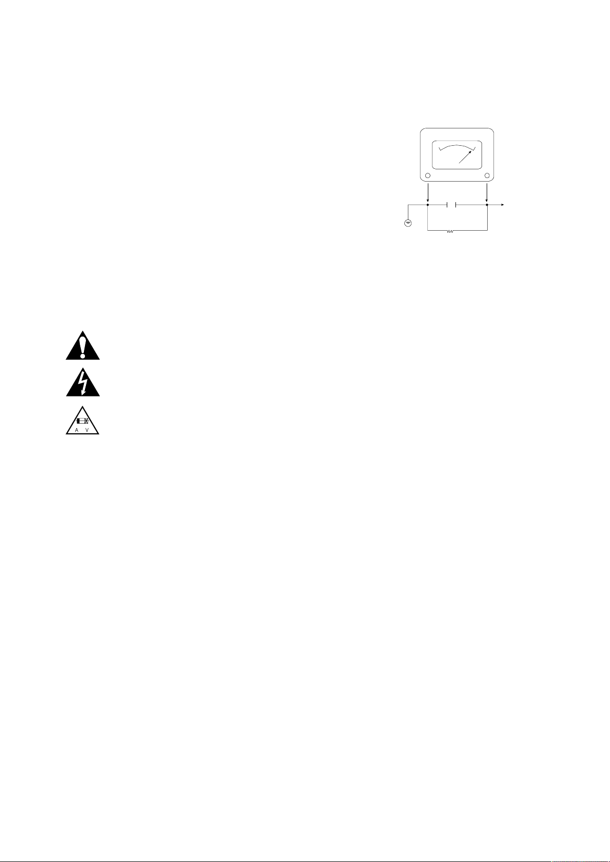
Good Earth Ground
such as the Water
Pipe, Conduit, etc.
A.C. Voltmeter
0.15uF
1500 OHM
10 WATT
Place this probe
on each exposed
metal part.
Page 4

1-3
SERVICING PRECAUTIONS
CAUTION: Before servicing the VCR + DVD RECODER covered by this service data and its supplements and addends,
read and follow the
SAFETY PRECAUTIONS. NOTE: if
unforeseen circumstances create conflict between the following servicing precautions and any of the safety precautions in this publications, always follow the safety precautions.
Remember Safety First:
General Servicing Precautions
1. Always unplug the VCR + DVD RECODER AC power cord
from the AC power source before:
(1) Removing or reinstalling any component, circuit board,
module, or any other assembly.
(2) Disconnecting or reconnecting any internal electrical
plug or other electrical connection.
(3) Connecting a test substitute in parallel with an elec-
trolytic capacitor.
Caution: A wrong part substitution or incorrect
polarity installation of electrolytic capacitors may result
in an explosion hazard.
2. Do not spray chemicals on or near this VCR + DVD
RECODER or any of its assemblies.
3. Unless specified otherwise in this service data, clean
electrical contacts by applying an appropriate contact
cleaning solution to the contacts with a pipe cleaner,
cotton-tipped swab, or comparable soft applicator.
Unless specified otherwise in this service data, lubrication
of contacts is not required.
4. Do not defeat any plug/socket B+ voltage interlocks with
whitch instruments covered by this service manual might
be equipped.
5. Do not apply AC power to this VCR + DVD RECODER
and / or any of its electrical assemblies unless all solidstate device heat sinks are correctly installed.
6. Always connect the test instrument ground lead to an
appropriate ground before connecting the test instrument
positive lead. Always remove the test instrument ground
lead last.
Insulation Checking Procedure
Disconnect the attachment plug from the AC outlet and turn
the power on. Connect an insulation resistance meter (500V)
to the blades of the attachment plug. The insulation resistance between each blade of the attachment plug and accessible conductive parts (Note 1) should be more than 1Mohm.
Note 1: Accessible Conductive Parts include Metal panels,
Input terminals, Earphone jacks,etc.
Electrostatically Sensitive (ES) Devices
Some semiconductor (solid state) devices can be damaged
easily by static electricity. Such components commonly are
called Electrostatically Sensitive (ES) Devices. Examples of
typical ES devices are integrated circuits and some field
effect transistors and semiconductor chip components.
The following techniques should be used to help reduce the
incidence of component damage caused by static electricity.
1. Immediately before handling any semiconductor component or semiconductor-equipped assembly, drain off any
electrostatic charge on your body by touching a known
earth ground. Alternatively, obtain and wear a commercially available discharging wrist strap device, which
should be removed for potential shock reasons prior to
applying power to the unit under test.
2. After removing an electrical assembly equipped with ES
devices, place the assembly on a conductive surface such
as aluminum foil, to prevent electrostatic charge buildup or
exposure of the assembly.
3. Use only a grounded-tip soldering iron to solder or unsolder
ES devices.
4. Use only an anti-static solder removal device. Some
solder removal devices not classified as “anti-static” can
generate electrical charges sufficient to damage ES
devices.
5. Do not use freon-propelled chemicals. These can
generate an electrical charge sufficient to damage ES
devices.
6. Do not remove a replacement ES device from its protective package until immediately before you are ready to
install it. (Most replacement ES devices are packaged with
leads electrically shorted together by conductive foam,
aluminum foil,or comparable conductive material).
7. Immediately before removing the protective material from
the leads of a replacement ES device, touch the protective
material to the chassis or circuit assembly into which the
device will be installed.
Caution: Be sure no power is applied to the chassis or
circuit, and observe all other safety precautions.
8. Minimize bodily motions when handling unpackaged
replacement ES devices. (Normally harmless motion such
as the brushing together of your clothes fabric or the lifting
of your foot from a carpeted floor can generate static electricity sufficient to damage an ES device.)
Page 5
THE STEPS FOR CHANGE THE OPTION CODE
Note : This procedure must be done when IC304(On digital Board) or Digital Board assy is replaced.
Push Switch POWER ON/ OFF
at remocon or timer keyborad
Select DVD MODE at the set
use remocon or timer keyborad
Push REC+ PLAY
at timer keyboard
Use remocon and push ENTER
Use Direction Key at
remocon (LEFT/ RIGHT)
for select the position of option
Use Direction Key
at remocon (UP/ DOWN)
for change the option
After finish edit code of option
push ENTER at remocon
For finishing and intialized
the option code push
REC+ FF at remocon
DETECT NEW EEPROM (OPTION EDIT SCREEN)
DVDR630VR/14
NAME HEX
OPT1 22
OPT2 48
OPT3 55
OPT4 95
OPT5 26
OPT6 9E
OPT7 D6
OPT8 D3
DVDR630VR/05
NAME HEX
OPT1 12
OPT2 47
OPT3 42
OPT4 95
OPT5 26
OPT6 9E
OPT7 F6
OPT8 D1
DVDR630VR/00
NAME HEX
OPT1 12
OPT2 44
OPT3 45
OPT4 95
OPT5 26
OPT6 9E
OPT7 F6
OPT8 30
DVDR630VR/02
NAME HEX
OPT1 02
OPT2 46
OPT3 52
OPT4 95
OPT5 26
OPT6 9E
OPT7 FE
OPT8 68
Press “Enter” key
to Save and Exit
1-4
Page 6
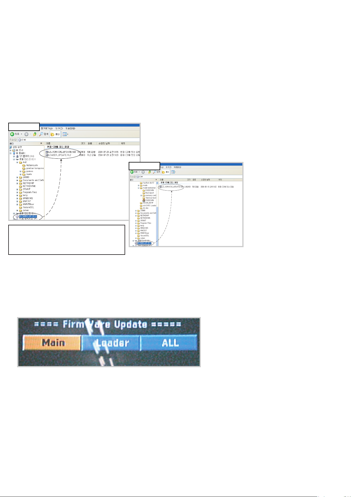
BURNING DISC
• For up-dating the DVD program using the disc, it must burning the disc which include the DVD software.
• For recorder combi set which using the disc downloader program are DVD Program and Loader Program.
• In 2nd generation for recorder combi can download the DVD program and Loader program one by one, or all
together.
• If you format like number 1 you’ll see capture like (figure 1)
• And you have three choice:
1. Main. It’s mean if you chose this it’ll up-dating only DVD prgram.
2. Loader.It’s mean if you chose this it’ll up-dating only Loader program.
3. ALL. It’s mean if you chose this it’ll up-dating DVD and Loader program.
• If you format like number 2 you’ll not see capture like figure 1 that give you choices, you have no choice only
update DVD program
1-5
UP-DATING PROGRAM
* There is two way to format disc DVD Program
1. DVD and LOADER program format in one
disc
2. Only DVD program format in one disc
(Figure 1)
Number 1
Number 2
Page 7
1-6
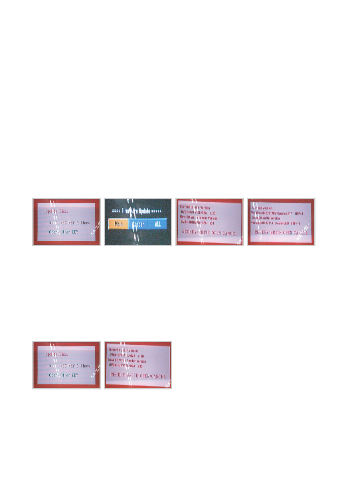
DVD UPGRADE INSTRUCTION
FORMAT NO 1
1. Press POWER KEY to turn on.
2. After booting, insert the upgrade disc, and you will see massage like [FIGURE 1]
3. Press “REC” key (front or remote) 3 times and you will see as [FIGURE 2] with remote Chose one of them
then Press enter
4. For update both of them [MAIN & LOADER] we chose “ALL” and first you will see [FIGURE 3] DVD update
→ Check the “Current Version” and “ New CD Write Version” and press “REC” key.
5. The DVD update will be on progress.And when finish update MAIN Version it’s automatically continue to
Update Loader Version and You will see [FIGURE 4]
→ Check the “Current Version” and “New CD Write Version “ and Press “REC” key once more
6. The LOADER update will be on progress. And tray will open.
7. Remove the disc and wait until finish
8. The tray will be close and open automatically after completing “UNDER UPDATE” 100%
9. Turn off the unit
10. Turn on again the unit is operation with new software
FORMAT NO 2
1. Press POWER KEY to turn on.
2. After booting, insert the upgrade disc, and you will see massage like [FIGURE 1]
3. Press “REC” key (front or remote) 3 times
4. The DVD update will be on progress.
→ Check the “Current Version” and “New CD Write Version “ and Press “REC” key once more
5. The tray will be open automatically after completing “UNDER UPDATE” 100%
6. Remove the disc andTurn off the unit
7. Turn on again the unit is operation with new software
[FIGURE 1] [FIGURE 2] [FIGURE 3] [FIGURE 4]
[FIGURE 1] [FIGURE 2]
Page 8

1-7
SPECIFICATIONS
General
Power requirements AC 220-230V, 50 Hz
Power consumption 35W
Dimensions (approx.) 430 X 78.5 X 354 mm (w x h x d)
Mass (approx.) 5.7 kg
Operating temperature 5°C to 35°C
Operating humidity 5 % to 90 %
Television system PAL B/G, PAL I/I, SECAM D/K color system
Recording format PAL
System
Laser Semiconductor laser, wavelength 650 mm
Video head system Double azimuth 4 heads, helical scanning
Signal system PAL
Recording
Recording format DVD+RW/+R Video format
Recordable discs DVD-ReWritable, DVD-Recordable, DVD+ReWritable, DVD+Recordable
Recordable time Approx. 1 hour (XP mode), 2 hours (SP mode), 4 hours (LP mode),
6 hours (EP mode)
Video recording format
Sampling frequency 27MHz
Compression format MPEG 2
Audio recording format
Sampling frequency 48kHz
Compression format Dolby Digital
Playback
Frequency response DVD (PCM 48 kHz): 8 Hz to 22 kHz, CD: 8 Hz to 20 kHz
DVD (PCM 96 kHz): 8 Hz to 44 kHz
.
Harmonic distortion Less than 0.008% (AUDIO OUT connector)
Dynamic range More than 95 dB (AUDIO OUT connector)
Inputs
AERIAL IN Aerial input, 75 ohms
VIDEO IN 1.0 Vp-p 75 ohms, sync negative, RCA jack x 1 / SCART x 2
AUDIO IN 0 dBm more than 47 kohms, RCA jack (L, R) x 1 / SCART x 2
DV IN 4 pin (i.LINK/IEEE 1394 standard)
S-VIDEO IN (Y) 1.0 V (p-p), 75 Ω, negative sync, Mini DIN 4-pin x 1
(C) 0.3 V (p-p) 75 Ω
Outputs
S-VIDEO OUT (Y) 1.0 V (p-p), 75 Ω, negative sync, Mini DIN 4-pin x 1
(C) 0.3 V (p-p) 75 Ω
COMPONENT VIDEO OUT (Y) 1.0 V (p-p), 75 Ω, negative sync, RCA jack x 1
(Pb)/(Pr) 0.7 V (p-p), 75 Ω, RCA jack x 2
Audio output (digital audio) 0.5 V (p-p), 75 Ω, RCA jack x 1
Audio output (analog audio) 2.0 Vrms (1 KHz, 0 dB), 600 Ω, RCA jack (L, R) x 1 / SCART
* Design and specifications are subject to change without notice.
* Manufactured under license from Dolby Laboratories. “Dolby”, “Pro Logic” and the double-D symbol are trademarks of
Dolby Laboratories.
* DTS and DTS Digital Out are registered trademarks of Digital Theater Systems, Inc.
Page 9

Page 10

SECTION 2
EXPLODED VIEWS
CONTENTS
EXPLODED VIEWS .....................................................................................................................2-2
1. Cabinet and Main Frame Section ...........................................................................................2-2
2. Deck Mechanism Section (RL-02A) (For information only).................................................2-3
3. Packing Accessory Section ....................................................................................................2-4
2-1
Page 11
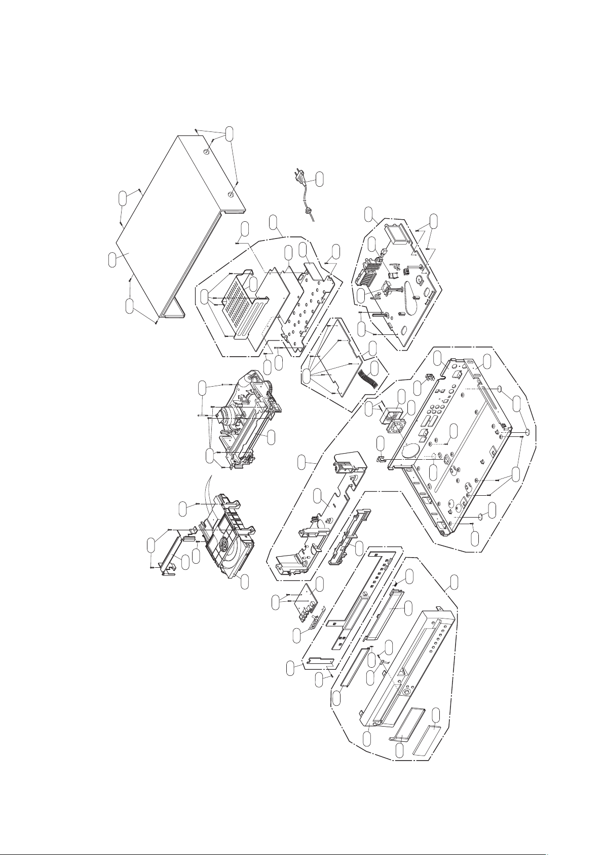
2-2
EXPLODED VIEWS
1. Cabinet and Main Frame Section
463
250
463
463
469
255
469
470
469
A47
470
256
257
469
300
469
323
469
A46
468
321
A52
290
263
264
265
469
320
261
261A
457
457
278
457
457
A60
A00
469
A50
274
A44
260
457
A48
285
276
287
286
266
469
283
284
261A
289
452
452
261A
452
A43
280
288
Page 12
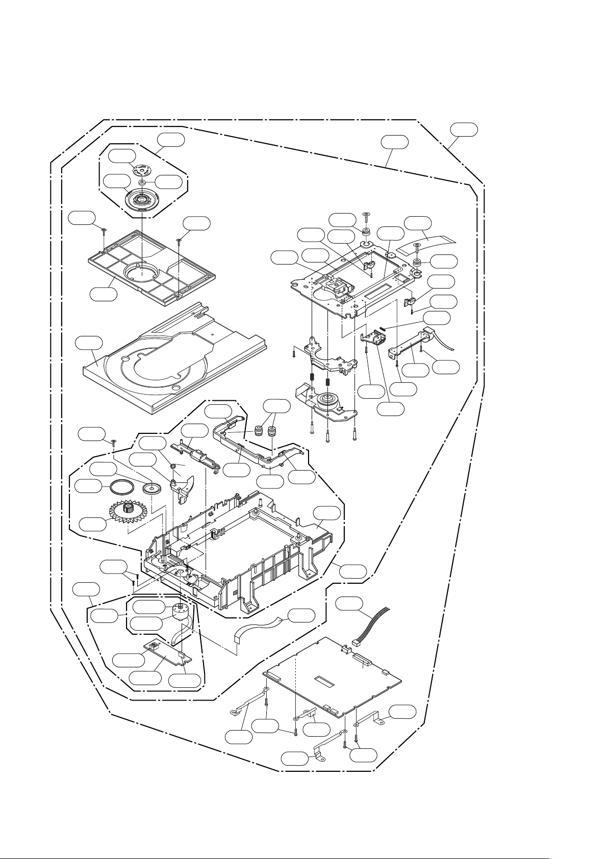
2. Deck Mechanism Section (RL-02A) - For information only
1434
1026
1003
1005
1001
A001
1002
1434
1019
1038
1024
1432
1028
1025
1027
1433
A000
1029
1432
1033
1030
1021
A60
1025
1027
1432
1032
1432
1435
1015
1017
A004
1016
1436
1018
1014
1018A
1018B
1018C
1018E
1013
1012
1018D
1009
1044
1011
1434
1019
1020
A002
1045
1006
CN101
1041
1042
2-3
1043
1434
Page 13
2-4
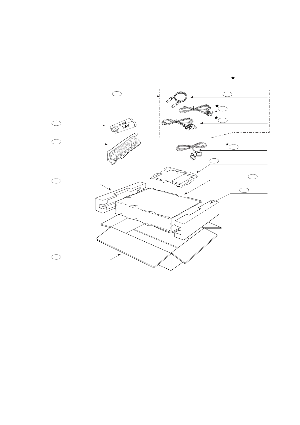
3. Packing Accessory Section
821
SCART CABLE
810
808
BATTERY
900
REMOCON
803
PACKING
CABLE ASS'Y RF
OPTIONAL PARTS
806
CABLE(COAXIAL)
811
PLUG ASS'Y 1WAY
812
PLUG ASS'Y 2WAY
INSTRUCTION ASSEMBLY
801
803
BAG
804
PACKING
802
BOX CARTON
Page 14

SECTION 3
ELECTRICAL
CONTENTS
OVERALL WIRING DIAGRAM............................................ 3-2
VCR PART
(includes SMPS Power, Jack, Key & Timer boards)
VCR ELECTRICAL ADJUSTMENT
PROCEDURES .................................................................... 3-4
VCR ELECTRICAL TROUBLESHOOTING
GUIDE................................................................................... 3-5
1. POWER (SMPS) CIRCUIT ....................................... 3-5
2. SYSTEM/KEY CIRCUIT ............................................3-8
3. SERVO CIRCUIT ......................................................3-9
4. Y/C CIRCUIT ........................................................... 3-12
5. HI-FI CIRCUIT ......................................................... 3-16
6. TUNER/IF CIRCUIT ................................................3-19
BLOCK DIAGRAMS ..........................................................3-21
1. POWER (SMPS) BLOCK DIAGRAM ..................... 3-21
2. TUNER/IF, NICAM & A2 BLOCK DIAGRAM ......... 3-23
3. VPS BLOCK DIAGRAM ..........................................3-24
4. Y/C BLOCK DIAGRAM ...........................................3-25
5. NORMAL AUDIO BLOCK DIAGRAM .................... 3-27
6. HI-FI BLOCK DIAGRAM .........................................3-29
7. SYSTEM BLOCK DIAGRAM ................................. 3-31
8. SCART & SWITCH BLOCK DIAGRAM ................. 3-33
CIRCUIT DIAGRAMS ........................................................3-35
1. POWER (SMPS) CIRCUIT DIAGRAM .................. 3-35
2. TUNER CIRCUIT DIAGRAM ................................. 3-37
3. A/V CIRCUIT DIAGRAM .........................................3-39
4. HI-FI CIRCUIT DIAGRAM .......................................3-41
5. SYSTEM CIRCUIT DIAGRAM ............................... 3-43
6. SCART (JACK) CIRCUIT DIAGRAM
(SCART MODEL ONLY) ......................................... 3-45
7. TIMER CIRCUIT DIAGRAM ................................... 3-47
* WAVEFORMS ......................................................... 3-49
* CIRCUIT VOLTAGE CHART...................................3-51
* IC BLOCK DIAGRAMS ...........................................3-55
PRINTED CIRCUIT DIAGRAMS .......................................3-59
1. VCR P.C.BOARD (TOP VIEW) .............................. 3-59
2. VCR P.C.BOARD (BOTTOM VIEW) ...................... 3-63
3. SMPS P.C.BOARD ..................................................3-65
4. JACK P.C.BOARD ...................................................3-68
5. KEY & TIMER P.C.BOARD .....................................3-69
VDR PART
VDR ELECTRICAL TROUBLESHOOTING
GUIDE.................................................................................3-71
1. POWER (SMPS) CIRCUIT ..................................... 3-71
2. NO COMPONENT VIDEO SIGNAL WHEN
PLAYING DISC .......................................................3-73
3. NO COMPOSITE / S-VIDEO SIGNAL WHEN
PLAYING DISC .......................................................3-74
4. NO TV, EXTERNAL INPUT VIDEO SIGNAL ......... 3-75
5. WHEN PLAYING DISC, NO AUDIO OUTPUT ...... 3-76
6. NO TUNER AUDIO OUTPUT ................................ 3-76
7. NO OPTICAL / DIGITAL OUTPUT ......................... 3-76
8. NO EXTERNAL INPUT 1 AUDIO........................... 3-77
9. NO EXTERNAL INPUT 2 AUDIO........................... 3-77
BLOCK DIAGRAMS ..........................................................3-78
1. VDR MAIN H/W BLOCK DIAGRAM ...................... 3-78
2. POWER BLOCK DIAGRAM ................................... 3-79
3. AUDIO IN/OUT BLOCK DIAGRAM ....................... 3-80
4. CPU & CONTROL REGISTER
BLOCK DIAGRAM ..................................................3-81
5. VIDEO IN/OUT BLOCK DIAGRAM ....................... 3-82
6. DV 1394 IN/OUT BLOCK DIAGRAM ..................... 3-83
7. MEMORY CARD IN/OUT BLOCK DIAGRAM ....... 3-84
CIRCUIT DIAGRAMS ........................................................3-85
1. BGA 308P CIRCUIT DIAGRAM ............................. 3-85
2. DDR & B TO B CONNECTOR
CIRCUIT DIAGRAM ................................................3-87
3. POWER, FLASH, CONNECTOR CIRCUIT
DIAGRAM ................................................................3-89
4. RST, CONTROL/STATUS_REG., ATAPI,
HOST_CPLD, LATCH CIRCUIT DIAGRAM .......... 3-91
5. VIDEO_IN, VIDEO_OUT CIRCUIT DIAGRAM ...... 3-93
6. DV1394, HDMI CIRCUIT DIAGRAM ..................... 3-95
7. AUDIO IN/OUT CIRCUIT DIAGRAM ..................... 3-97
* WAVEFORMS ......................................................... 3-99
* CIRCUIT VOLTAGE CHART................................ 3-101
* IC BLOCK DIAGRAMS ........................................ 3-103
PRINTED CIRCUIT DIAGRAMS .................................... 3-107
1. VDR P.C.BOARD (TOP VIEW) ............................ 3-107
2. VDR P.C.BOARD (BOTTOM VIEW) ..................... 3-111
RL-02A LOADER PART
(FOR INFORMATION ONLY).......................... 3-113 TO 3-184
3-1
Page 15

Page 16
15
14
13
12
11
10
9
8
7
6
5
4
3
2
1
123456789
1011121314151617181920
21
123456789
1011121314151617181920
21
SPD.F
GND
INTR/PROG
NC
GND
RADIO'H'
AMP ON
VDR REDET
NCNCNC
VDR CLK
DATA(VCR-VDR)
DATA(VDR-VCR)
VDR ENA
AMP CLK
AMP RX
AMP TX
AMP READY
AMP MUTE
NC
15
14
13
12
11
10
9
8
7
6
5
4
3
2
1
P6603
P6602
PM601PN302
PN302
PN301
PN301
PMD01
PMD02
PN304
CON401
CON401
PPM01
P101
P3D01
P3D03
P104
P103
P103
P104
P3D02
P3D02
PMC01
PMC01
P3D03
P3D01
PN303
PM602
PM603 P6M01
13.5VA(DRUM)
A/E(-)
A/E(+)
CFG
CAP.VCC
SERVO VCC
CAP.REV'H'
I-LIMIT
MOTOR GND
S.GND
DRUM VCC(13.5VA)
CAP.CTL
L/M CTL
DPG/DFG
DRUM CTL
8.7V
GND
1
2
1
2
R493
3-2
3-3
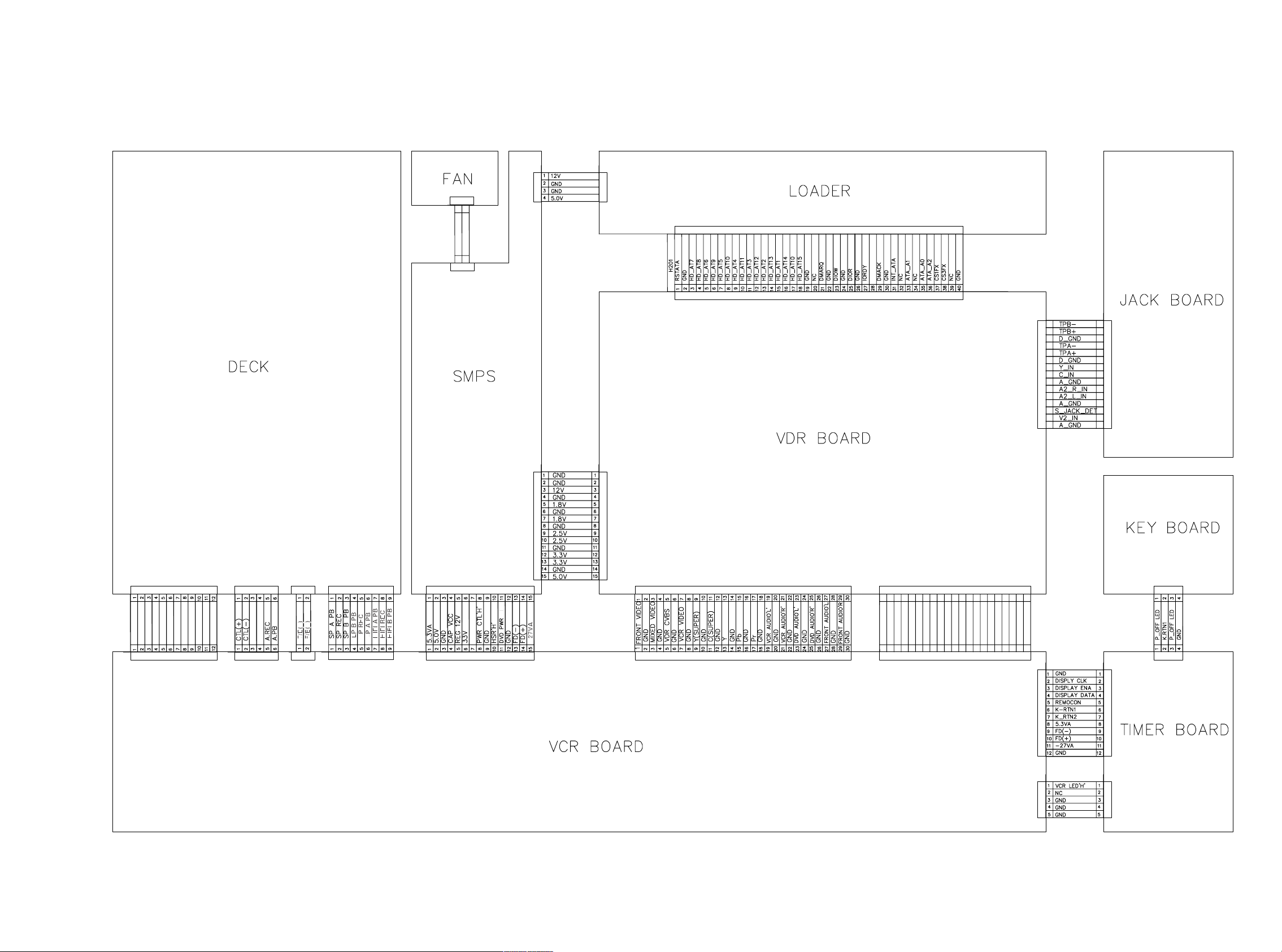
OVERALL WIRING DIAGRAMS
Page 17
Page 18
3-4
ELECTRICAL ADJUSTMENT PROCEDURES
1. Servo Adjustment
1) PG Adjustment
• Adjustment And Specification
• Test Equipment
a) OSCILLOSCOPE : PAL SP TEST TAPE
MODE
PLAY
• Adjustment Procedure
a) Insert the SP Test Tape and play.
b) Connect the CH1 of the oscilloscope to the H/SW and CH2 to the “VCR VIDEO” TP for the VCR.
c) Trigger the mixed Combo Video Signal of CH2 to the CH1 H/SW, and then check the distance (time dif-
ference), which is from the selected A(B) Head point of the H/SW signal to the starting point of the vertical synchronized signal, to 6.5H ± 0.5H (416µs, 1H=64µs).
• PG Adjustment Method
a-1) Playback the SP standard tape
b-2) Wait for 3seconds with F/P “REC” key and “PLAY” key presseed at the same time. < Digitron[ - - ] >
c-3) Repeat the above step(No.b-2), then it finishes the PG adjusting automatically. < Digitron[ PG ] >
d-4) Stop the playback, then it goes out of PG adjusting mode after mony the PG data.
• CONNECTION
• WAVEFORM
V.Out
H/SW(TP)
R/C TRK JIG KEY 6.5 ± 0.5H
MEASUREMENT POINT ADJUSTMENT POINT SPECIFICATION
H/SW
(TP)
TP
(VCR
VIDEO)
(CH2)
(CH1)
OSCILLOSCOPE
CH1 CH2
R/C KEY
H/SW
(TP)
VCR BOARDVDR BOARD
"VCR VIDEO" TP
VCR PART
H/SW
Composite
VIDEO
6.5H(416µs)
Page 19
3-5
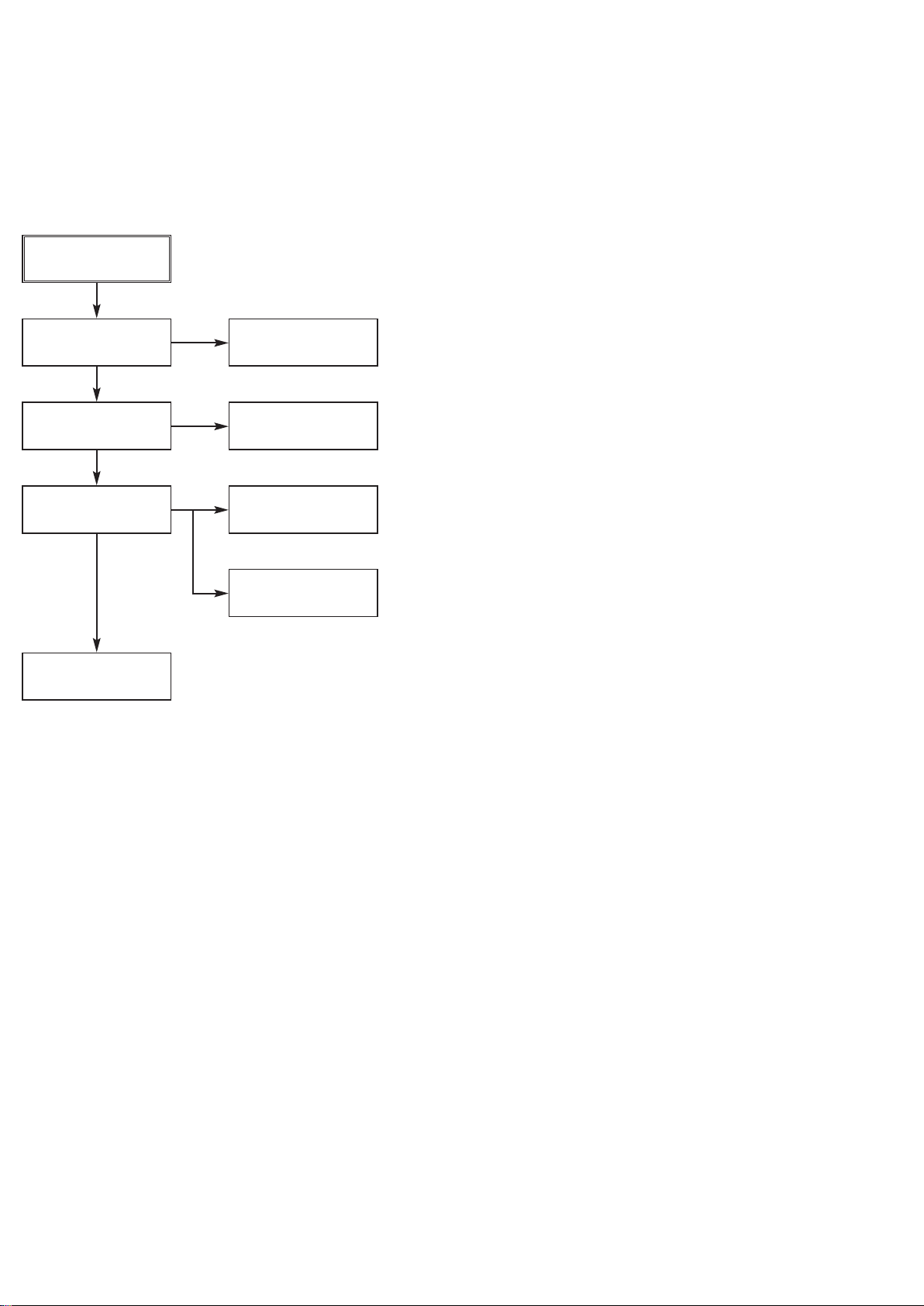
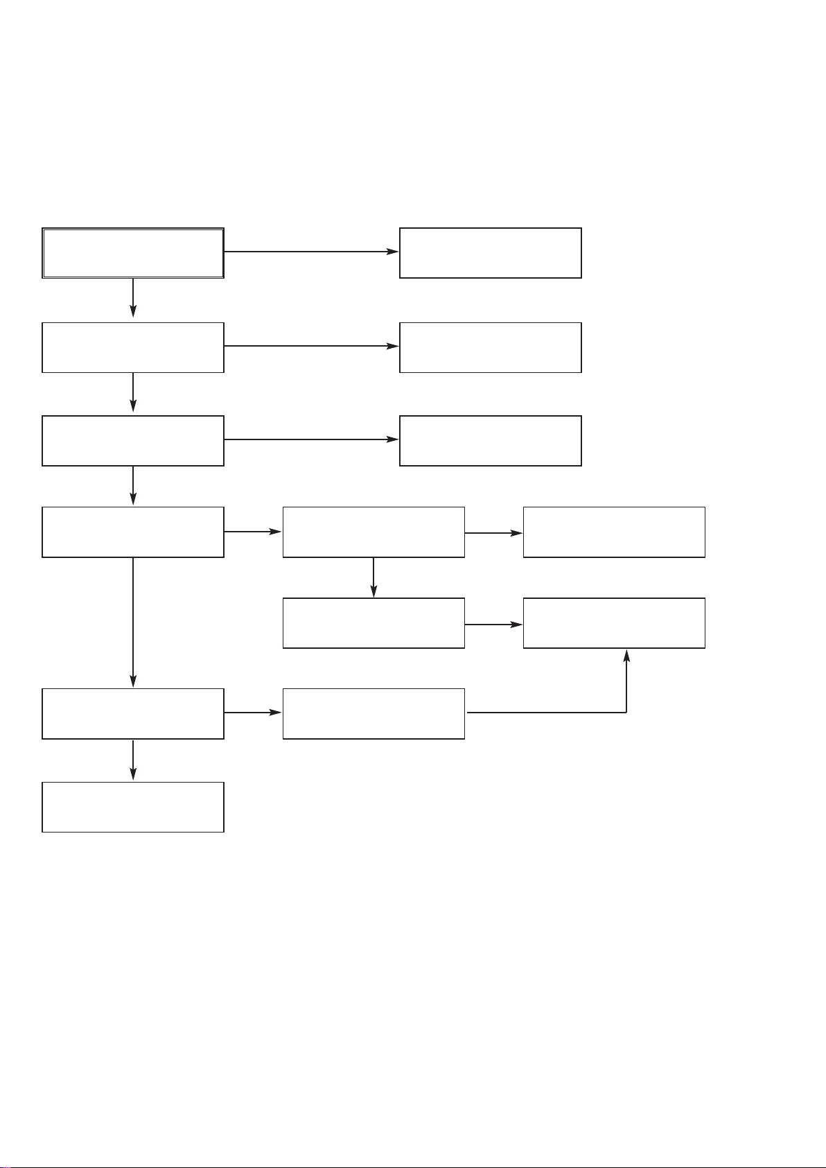
VCR ELECTRICAL TROUBLESHOOTING GUIDE
1. Power(SMPS) CIRCUIT
NO 5.3VA.
Replace the F101
(Use the same Fuse)
Is the F101 normal?
Is the TH01
Normal?
Is the BD101
Normal?
NO
NO
NO
NO
NO
NO
NO
NO
NO
NO
NO
Replace the BD101
Replace the TH01
Is the D102
normal?
Check or Replace
the D102
Replace the D121
Replace the IC103
Replace the D126
Replace the D129
Replace the D130
Replace the D127
Replace the D128
YES
YES
YES
YES
YES
YES
YES
YES
YES
YES
Is the Vcc (11V - 18V)
supplied to IC101 Pin2?
NO
Is the D121
normal?
Is there about 2.5V
at the IC103 Pin1?
Is the D126
normal?
Is the D129
normal?
Is the D130
normal?
Is the D127
normal?
Is the D128
normal?
YES
Power Line of Main
PCB(VCR) is short
Page 20
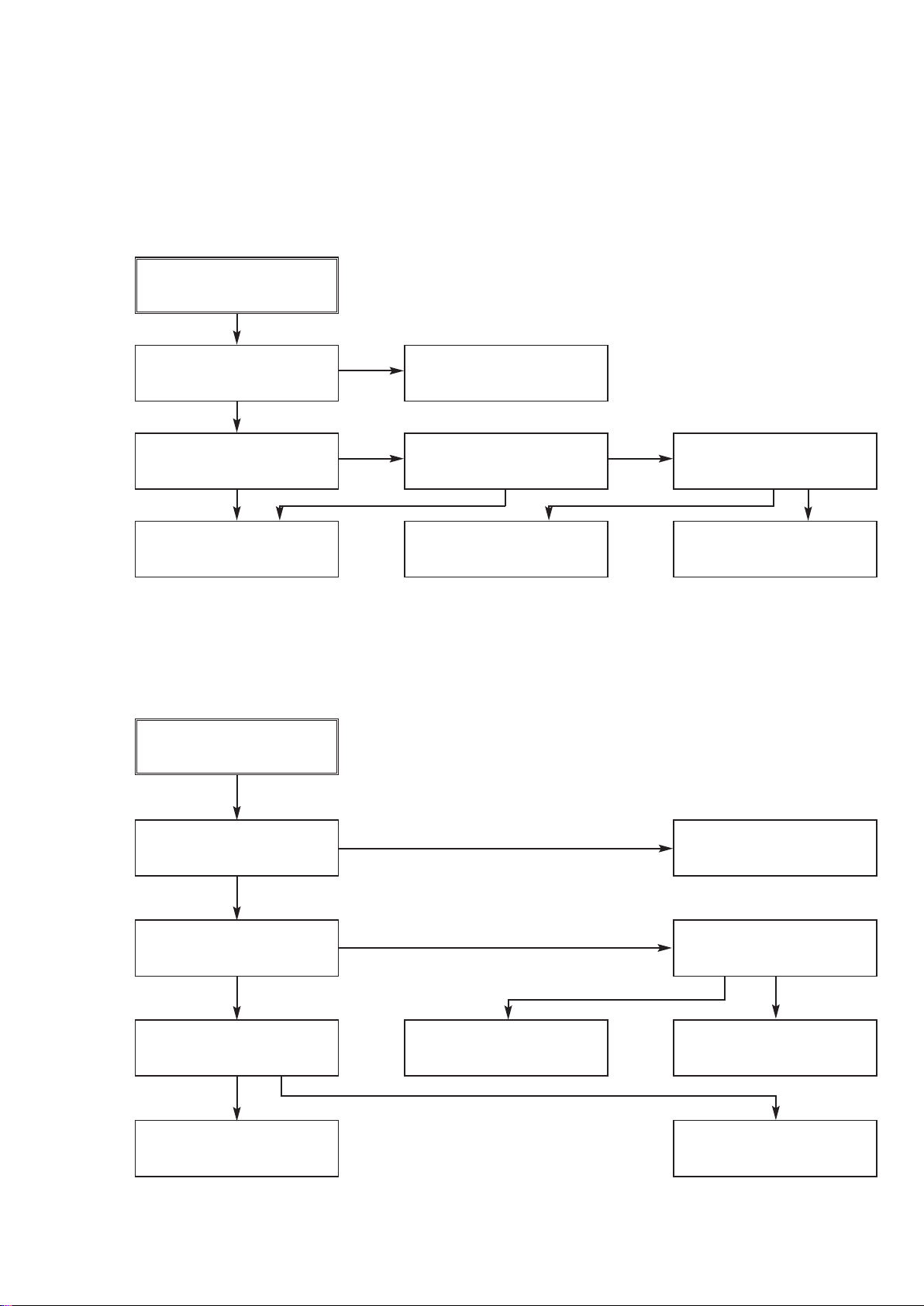
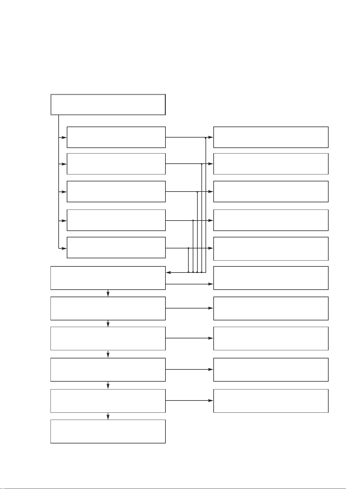
3-6
VCR ELECTRICAL TROUBLESHOOTING GUIDE
No 12VA
Check or Replace
the D126
Is the Vcc(13V)
supplied to C130?
Check or Replace
the Cap / Drum
Is the D132
Normal?
NO
NO
Replace the D132
YES
YES
(To Cap, Drum Motor )
No REG 12V
Check or Replace
the D126
Check the ‘PWR CTL
“H”’signal from µ-com
Check the 33V Line
Replace the Q126
Is the Vcc(13V) supplied to Q126Collector?
Is the Vcc(33V) supplied to Q126 Base?
Is the Q126 Nomal?
Check or Replace
the D126
NO
NO
NO
YES
YES
YES
NO VFD
Check or Replace
the R107
Is the R107
Normal?
Is the D128
Normal?
NO
Check or Replace
the D128
Check or Replace
the ZD151
NO
NO
YES
Is the ZD151
Normal?
Check or Replace
the D127
YES
YES
No 33V
Check or Replace
the D130
Is the Vcc(33V) supplied to Q123 Emittor?
Is the Q123 Base
‘H’?
NO
Check the ‘PWR CTL
“H”’signal from µ-com
NO
YES
Check or Replace
the Q123
YES
Page 21
3-7
VCR ELECTRICAL TROUBLESHOOTING GUIDE
No 28V (HSR)
Check or Replace
the D129
Is the Vcc(30V) supplied
to Q120 Collector?
Is the Vcc(33V) supplied
to Q121 Collector?
Is the Vcc(30V) supplied to Q120 Base?
NO
NO
Check or Replace
the ZD153
NO
Check the ‘HSR “H”
signal from µ-com
Check or Replace the
Q121/Q122 & 33V line
YES
YES
Check or Replace
the Q120
YES
Page 22
3-8
2. SYSTEM/KEY CIRCUIT
(1) AUTO STOP
(2) The unstable loading of a Cassette tape
Auto Stop
Does the H/SW waveform
appear at IC501 Pin23?
Do the T-UP Reel Pulses
appear at IC501 Pin3?
Is 12V applied to PMC01
Pin8?
Check the Drum Motor
signal.
Does 5.0V appear at the
RS501?
Check the Power Circuit.
Check the power.
Is 5.0V applied to the
R544 ?
Refer to SMPS 5.3VA
troubleshooting.
Check IC501
Pins86, 87, 88, 89.
Do T/UP Reel Pulses
appear at the Q514 Base
terminal?
Replace the T/UP Reel
Sensor (RS501).
Check the CST SW and
the peripheral circuitry.
Replace the IC501.
The unstable loading of a
Cassette tape
Does the “H” signal appear
at IC501 Pin32 during
inserting the CST ?
Does the “L” signal appear
at IC501 Pin19 while
inserting the CST?
Check the Deck
Mechanism.
Note :
Auto stop can occur because Grease or Oil has dried up
YES
YES
NO
YES
YES
YES
NO
NO
NO
NO
NO
NO NO
YES
YES YES
VCR ELECTRICAL TROUBLESHOOTING GUIDE
Page 23
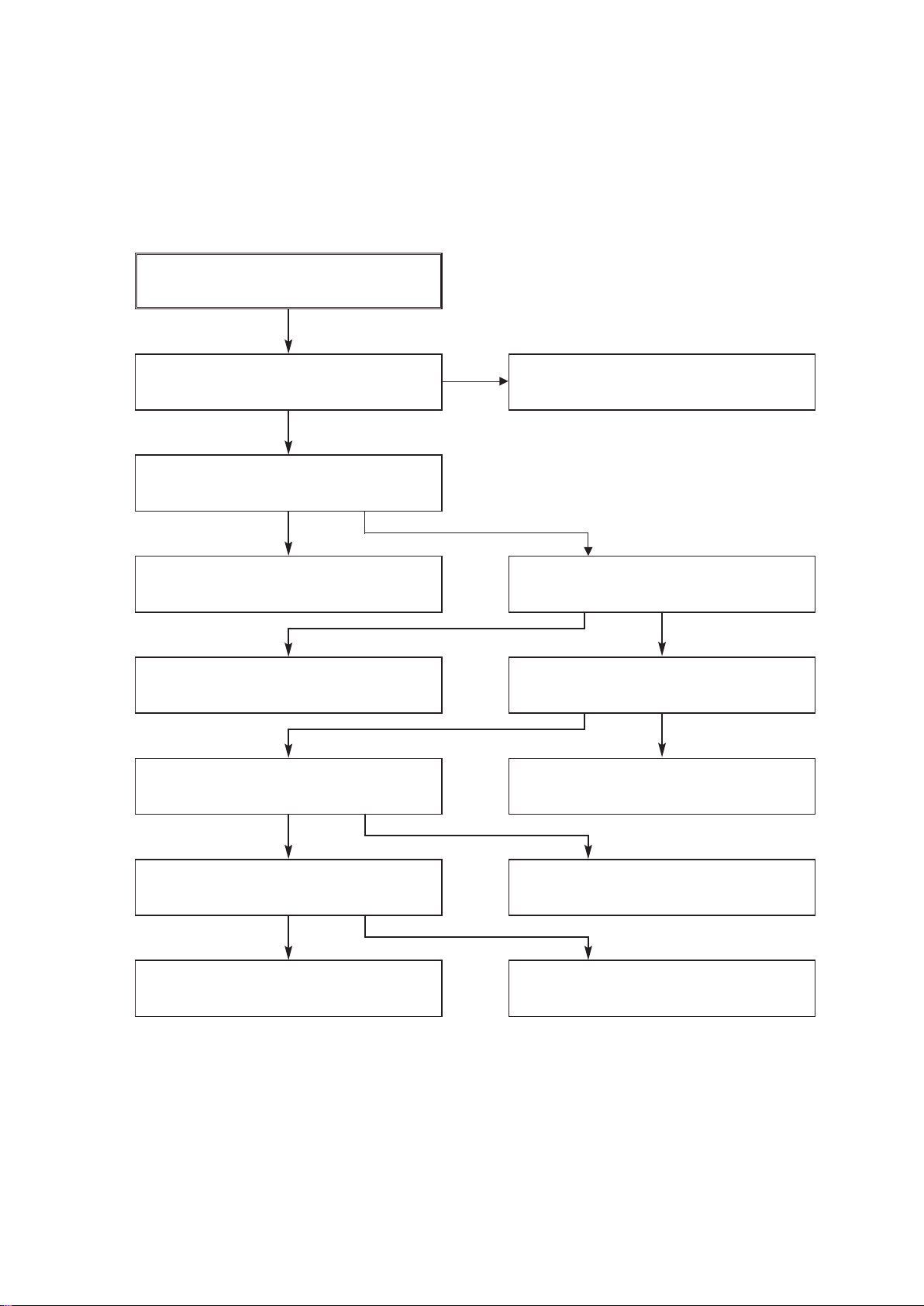
3-9
3. SERVO CIRCUIT
(1) Unstable Video in PB MODE
Does the Noise level of the
screen change
periodically?
Do the CTL pulses appear
at IC501 Pin8?
Is adjusting the height of
the CTL Head accurate?
Readjust the height of the
CTL Head.
Replace the IC501.
Refer to “When the Y signal
doesn’t appear on the
screen in PB Mode”.
Does the CFG waveform
appear at the IC501 pin9?
On tracking, do the CTL
pulses move?
Does the Video Envelope
waveform appear at IC501
Pin24?
Replace IC501.
YES
YES
YES
NO NO
NO
NO
(2) When the Drum Motor
(2) doesn’t run.
Do the DFG Pulses appear
at PMC01 Pin11?
Replace the Cap M.
Aren’t the foil patterns and
the Components between
IC501 Pin 104 and PMC01
Pin11 shorted?
Replace the IC501.
Refer to “(2)
No 12VA of Power section”
Do the Drum PWM Pulses
appear at IC501 Pin107?
Aren’t the foil patterns and
the Components between
IC501 Pin107 and PMC01
Pin12 shorted?
Do the DFG Pulses appear
at IC501 Pin104?
Do the Drum PWM Pulses
appear at IC501 Pin107?
Are the connecting patterns and the Components
between IC501 Pin107 and PMC01 Pin12 shorted?
When the Drum Motor
doesn’t run,
Does 12V appear at
PMC01 Pin8?
Does 2.8V appear at
PMC01 Pin12?
Check the connector
(PMC01) and the Drum
Motor Ass’y.
NO
YES
YES
YES
NO
NO
NO
NO
NO
YES
YES
YES
VCR ELECTRICAL TROUBLESHOOTING GUIDE
Page 24
3-10
Does the CFG signal appear at
PMC01 Pin1?
Does the PWM signal appear at IC501
Pin108?
Does 2.8V appear at PMC01?
Check the PMC01 and the Capstan
Motor Ass’y.
Does the Capstan PWM signal appear at
IC501 Pin108?
Aren’t the foil patterns and Components
between IC501 Pin108 and PMC01
Pin9 short?
Does the CFG signal come into IC501
Pin9?
Aren’t the foil patterns and Components
between IC501 Pin108 and PMC01
Pin9 short?
2. SERVO CIRCUIT
(3) When the Capstan Motor doesn’t run,
NO
NO
NO
YES
YES
YES
When the Capstan Motor doesn’t run,
Does 12VA appear at PMC01?
YES
Replace the IC501.
YES
NO
NO
YES
Refer to “SMPS(CAPSTAN/12Volt)
Trouble Shooting”.
Aren’t the foil patterns and component
between IC501 Pin87 and PMC01
Pin1 shorted?
Check the Capstan Motor Ass’y.
NO
VCR ELECTRICAL TROUBLESHOOTING GUIDE
Page 25
3-11
Keys do not work
Is 5V applied to IC501
Pin36?
Does FLD change when
a function button is
pressed?
Refer to “SMPS 5.3VA
Trouble Shooting”.
Replace the defective
switches.
YES
NO
NO
2. SERVO CIRCUIT
(4) Keys do not work
VCR ELECTRICAL TROUBLESHOOTING GUIDE
Page 26
3-12
4. Y/C CIRCUIT
(1) No Video in EE Mode,
No Video in EE Mode
Does the Video signal
appear at IC301 Pin48?
Check the 19Pin
Is REG 5.0V applied to
IC301Pins18, 24, 42, 55, 72,
91?
Does the Video signal
appear at IC301 Pin65?
Does the Video signal
appear at the IC901
Pin23?
Does the Video signal
appear at the PMD02
Pin7?
Does the Video signal
appear at the PMD02
Pin5?
Check the 5.0V, 5.3VA
Line. (Power Circuit)
Is I2C BUS signal applied to
the IC301 Pins68, 69?
Check C316. (AGC)
Replace IC301.
Does the 12VT, 5.3VA
appear at the IC901 Pin3, 4.
Check the 12V, 5.4VA
Line. (Power Circuit)
Check the Video Buffer
Q905.
Check the DVD Board
Video path.
Check the System Circuit.
(Refer to ‘SYSTEM I
2
C BUS
CHECK Trouble Shooting’)
YES
YES
YES
YES
YES
YES
YES
Replace IC901.
YES
NO
NO
NO
NO
NO
NO
NO
NO
VCR ELECTRICAL TROUBLESHOOTING GUIDE
Page 27
3-13
3. Y/C CIRCUIT
(2) When the Y(Luminance) signal doesn’t appear on the screen in PB Mode,
Is 5.0V 5.3VA applied to IC301
Pins24, 42, 55, 72, 91?
Is I2C BUS signal applied to
the IC301 Pins68, 69?
Does the normal RF signal
appear at IC301 Pin 78?
Check the line of the 5.0V
5.3V Line. (Power Circuit)
Check the System Circuit.
(IC501 Pin23)
Check the V.H.S/W level.
(Check R303, R304)
Refer to ‘SYSTEM I2C
BUS CHECK Trouble
Shooting’.
Is the V.H.S/W signal
applied to IC301 Pin70?
Is the V.H.S/W “H” about
3.4V at the IC301 Pin70?
Clean the Drum.
Check the path of the
Y(Luminace) RF signal.
(Check the C327)
Check the path of the
Y(Luminace) RF signal.
(Check the C312)
Does the Y(Luminance)
RF signal appear at
IC301 Pin79?
Is the Y(Luminance) Video
waveform showed up at
IC301 Pin43?
Replace IC301.
NO
YES
YES
YES
YES
YES
YES
YES
NO
NO
NO
NO
NO
NO
Replace the IC301.
NO
VCR ELECTRICAL TROUBLESHOOTING GUIDE
Page 28
3-14
3. Y/C CIRCUIT
(3) When the C(Color) signal doesn’t appear on the screen in PB Mode,
Is 5.0V 5.3VA applied to the
IC301 Pins24, 42, 55, 72, 81.
Does the Color signal
appear at IC301
Pin25?
Check the line of the 5.0V
5.3VA Line. (Power Circuit)
Replace the X301.
Check the Color Pass.
Does the X301
(4.43MHz) osxillate?
Replace the IC301.
Does the Color signal
appear at IC301 Pin48?
Replace the IC301.
NO
YES
Is the Color Rotary signal
applied to the IC301 Pin70?
Check the Color Rotary
Circuit. (IC501 Pin98)
NO
YES
Is Color Rotary “H” about
3.4V?
NO
Check the Color Rotary
level. (Check the R303)
YES
YES
YES
NO
NO
NO
VCR ELECTRICAL TROUBLESHOOTING GUIDE
Page 29
3-15
3. Y/C CIRCUIT
(4) When the Video signal doesn’t appear on the screen in REC Mode,
VCR ELECTRICAL TROUBLESHOOTING GUIDE
Is the EE signal normal?
Does the RF signal
appear at the IC301
Pin78?
Check EE Mode.
Check the System of REC
‘H’.(the IC501 Pin27 / the
D301)
Replace the IC301.
Is the REC ‘H’ signal
(about 4V) applied to the
IC301 Pin80?
Check the circuit of the
IC301 Pin85, 86.
Check REC Luminace pass
& Color pass.
Does the REC RF signal
appear at the IC301
Pins88, 89, 94, 95?
NO
YES
Is 5.0V 5.3VA applied to the
IC301 Pins24, 42, 55, 72,
91?
Check the line of the 5.0V
5.3VA line. (Power Circuit)
NO
YES
Does PB Mode operate
nomally?
NO
Check PB Mode.
YES
Check the Drum & Drum
Connector
YES
YES
YES
NO
NO
NO
NO
Page 30
3-16
VCR ELECTRICAL TROUBLESHOOTING GUIDE
5. Hi-Fi CIRCUIT
(1) No Sound(EE Mode)
YES
No Sound.
Check the AV1 Audio of IC801
Pins6, 7.
Check the AV2 Audio of IC801
Pins8, 9.
Check the AV3 Audio of IC801
Pins10, 11.
Check the Vcc of IC801 Pins34, 40,
IC804 Pin13.
YES
Check the IIC Clock and DATA at
IC801 Pins42, 43.
YES
YES
Check the Audio of IC801 Pins16, 17.
Check the SC901, JK901.
Check the Scart1 Jack.
(SC901 Scart1 Audio in Pin2, 6).
NO
NO
Check the Scart2 Jack.
(SC901 Scart2 Audio in Pin2, 6).
NO
Check the front Jack.
Check the Power 5.0V, 12V.
YES
NO
Check the IC501 Pins59, 60.
NO
Replace IC801.
NO
Check the Audio of PMD02 Pin19, 21.
Check the Pcb Pattern between IC801
Pin16, 17 with PMD02 Pin19, 21.
NO
YES
YES
Check the Audio of PMD02 Pin23, 25. Check the DVD Board Audio path.
NO
Check the TU Audio of IC801
Pins2, 3.
Check the IC751 Pin30, 31.
NO
Check the DVD Audio of IC801
Pins4, 5.
Check the DVD Audio OUT.
(JK902 DVD_A_L_L/R).
NO
Page 31

3-17
VCR ELECTRICAL TROUBLESHOOTING GUIDE
3. Y/C CIRCUIT
(2) Hi-Fi Playback
YES
YES
YES
YES
PB mode
No Sound.
Check the Vcc of IC801
(Pins34, 40)
Check the Hi-Fi Selection switch.
(IC801 Pin41) and the Tape quality.
Is the RF Envelope at
IC801 Pin44 over 2Vp-p?
YES
Check IC801 Pin42(Data),
Pin43(Clock)
YES
Do Audio Signals appear at
IC801 Pin16(L-CH), 17(R-CH)?
YES
Do Audio Signals appear at
IC804 Pin3(L-CH), 5(R-CH)?
YES
Do Audio Signals appear at
JK902?
YES
Check the IC804, C844,
C845, C846, C 847
Check Power 5.0V, 12V.
NO
Check IC501 Pin26
(A.H/SW)
NO
NO
Check the parts of µ-COM
(IC501 Pins17, 18)
NO
Check the Connection at
P3D01 Pins7, 9.
NO
Check the Audio PMD02
Pin23, 25.
NO
Check the Jack(JK902)
NO
Check the DVD Board
Audio Path
NO
Page 32

3-18
(3)
Hi-Fi REC.
It can’t be recorded Hi-Fi Audio
signal.
Check Vcc of IC801. (Pins34. 40)
YES
YES
Check IC801 Pin42(Data), Pin43(CLOCK).
YES
Do Audio signals appear at IC801
Pins16, 17?
YES
Do FM Audio signals appear at IC801
Pin36?
YES
Check the Contact Point of Drum
Connector if good then Replace the Drum.
YES
Check Power 5V, 12V.
NO
Check ports of µ-COM.
(IC501 pins 17, 18)
Check Audio input signal of IC801
Pins2, 3(TU.A.), 4, 5(DVD.A.), 6,
7(AV2.A.), 10, 11(AV3.A).
NO
Replace IC801.
NO
NO
VCR ELECTRICAL TROUBLESHOOTING GUIDE
Page 33

3-19
6. Tuner/IF CIRCUIT
(1) No Picture on the TV screen
No picture on the TV
screen
Does the Video signal
appear at TU701 Pin19.
YES
Is 33V applied to TU701
Pin17?
Is +5V applied to TU701
Pin4?
NO
Does the video signal at
the PMD02 Pin5?
NO
Does the Video signal at
the IC301 Pin 63.
NO
Does the Video signal at
the IC901 Pin 10.
Check 33V line.
NO
Check 5V line.
NO
Does the Clock signal
appear at TU701 Pin12?
Check the llC Clock Signal
of µ-COM Pin18.
NO
Does the data signal
appear at TU701 Pin13?
Replace Tuner.
Check the DVD Board
Video Path.
Replace the IC301.
NO
Replace the IC901.
Does the video signal
appear at IC301 Pin48.
NO
YES
YES
YES
YES
YES
YES
YES
YES
YES
Check the Pattern between IC901
Pin10 with SC901 Pin19
Does the Video signal at
the IC301 Pin65.
NO
Check the Pattern between
TU701 Pin19 with IC301
Pin48.
Replace the IC301.
Check the llC Data Signal
of µ-COM Pin17.
NO
VCR ELECTRICAL TROUBLESHOOTING GUIDE
Page 34

3-20
VCR ELECTRICAL TROUBLESHOOTING GUIDE
(B) No Sound
No Sound.
Check the Vcc of IC701 Pins1, 11, 19,
22, 33.
YES
Check 5.2V Line.
NO
Check the Tuner SiF signal at IC751
Pin2.
YES
Check the oscillator of IC751 Pins5, 6.
YES
Check the Audio of IC751 Pins30, 31.
YES
Check the Audio of IC801 Pins2, 3.
YES
Check the Audio of IC801 Pins16, 17.
YES
Check the Tuner SIF of TU701 Pin16.
NO
Replace X751
NO
Check the IIC Clock and Data at IC751
Pins12, 13.
NO
Check the signal flow from IC751
Pins30, 31 to IC801 Pins2, 3.
NO
Check the IIC Clock and Data at IC801
Pins42, 43.
NO
Check the Audio of IC804 Pins3, 5.
YES
Check the Signal flow from IC804 pin3, 5
Sc901 Pins1, 3.
YES
Check the DVD Board Audio Path.
NO
Page 35

Page 36

3-21
3-22
BLOCK DIAGRAMS
1. POWER(SMPS) BLOCK DIAGRAM
BD
101
!
NOISE FILTER
BLOCK
(C101,L102,
L101, C102)
!
FUSE
(F101)
BR BL
(BK)(WH)
!
Y-CAP
C110
TH01
C103
!
+
Y-CAP
111
C
SNUBBER
BLOCK
(D101,C105
C106,R103)
5
5
1
6
DRIVE & S/W BLOCK
(IC101, D102, R105,
C108,C1
SNUBBER
BLOCK
(D103,C115,C116
,R112,R115)
6
DRIVE & S/W BLOCK
(IC104, D104, R113,
C117,C114)
!
T101
7
8
12)
3
7
8
3
2
!
PHOTO COUPLER
C102)
(I
102
T
!
2
!
PHOTO COUPLER
(I
RECTIFIER &
SMOOTING BLOCK
(D128,C133,R130)
RECTIFIER &
SMOOTING BLOCK
(D126,C136,L122,C1
RECTIFIER &
SMOOTING BLOCK
(D129,C128,R147)
RECTIFIER &
SMOOTING BLOCK
(D130,C137,R146)
RECTIFIER &
SMOOTING BLOCK
(D121,C122,L121,C124)
FEED-BACK
R121,R122,
ERROR AMP
(IC103)
RECTIFIER &
SMOOTING BLOCK
(D125,C139,L127,C140)
RECTIFIER &
SMOOTING BLOCK
(D124,C129)
RECTIFIER &
SMOOTING BLOCK
(D123,C126,L124,C127)
RECTIFIER &
SMOOTING BLOCK
(D122,C123,L123,C1
C105)
ERROR AMP
(IC106)
C121,R123.
R124.R125
FEED-BACK
R131,R132,
C141,R133.
30)
BLOCK
R126)
25)
BLOCK
R161.R162
R163)
RECTIFIER &
SMOOTING BLOCK
(D127,C131,L125,C132)
HSR S/W Block
(Q120,ZD153,C135,
R144,R145,D155,C157)
12V REG & S/W Block
(Q126,R150,ZD152,
C156,C153)
33V S/W Block
(Q123,R143,R13
5.0V S/W Block
(Q124,R140,R135,R136
D134,C134
HSR CTL Block
(Q121,Q122,R141)
PWR CTL Block
(Q125,R137,R13
12V REG & S/W Block
(IC157,R156,C155)
5.0V REG & S/W Block
(IC151,R151,C151)
1.8V REG & S/W Block
(IC160,R159,C152)
3.3V REG & S/W Block
(IC154,R154,C154)
4)
TO VCR
(P101)
5.3VA
5.0V
Cap Vc
c
REG 12V
33V
12VA( DRUM)
PWR CTL 'H'
HSR 'H'
DVD PW
R CTL
FD(-)
FD( +)
)
-28VA
TO FAN
(P103)
8)
8.7V
TO VDR
(P102)
-12V
12V
1.8V
2.5V
3.3V
5.0V
TO LOADER
(P103)
12V
5.0V
VCR+DVD REC SCART+RCA
Page 37

2. TUNER/IF, NICAM & A2 BLOCK DIAGRAM
SW1
SW2
AS
151 5.4VA
871
159
872
S.V.W
(From Power)
158
94
93
59
60
3. VPS BLOCK DIAGRAM
A.OUT
AFT
SIF
MSP3417
MSP3407
27
159
731
VCR+DVD REC SCART+RCA
3-23
3-24
Page 38

3-25
3-26
4. Y/C BLOCK DIAGRAM
(PB Mode)
(REC Mode)
S1 V.OUT
S2 V.OUT
(MICOM)
V.OUT
C.SYNC
CLOCK
DATA
C.ROTARY
V.H .S W
65 63 61
69 68 67
70
Y/C MIX
60dB AMP
MAIN
DE EMP
SUB LPF
AGC
PB FM
Y-L PF
PB FM EQ FM OEM
46
YNR
43
Y-Delay
IC301
LA71750M
(1H/2H)
C-Delay
BPF
MAIN
CONV
ACCC LPF
LPF
CCD
DET
ACC
SYNC IN
29
CNC
IC201
LA70100M
18 14
2521
CLOCK
DATA
C.ROTARY
V.H .S W
DEC
V.IN3
FRONT
V.IN4
MICOM
V.OUT
C SYNC
2 12
29 16
IC201 LA70100M
V.IN1 TUNER
50 V.IN2 S1
48
SW
AGC
NL
EMPHA
W/D
CLIP
DETAIL
W/D
ENH
CLIP
Y-L PF FBC
46
REC
FM EQ
43
Y-DELAY
YNR
1H/2H
DELAY
BPF
IC301
LA71750M
AMP
COMP
Main
Conv
Main
Conv
Killer C-LPF ACC
33
KILL DEC
32
31
VX02 VX02
REC APC
CLK-IN
2928
4.43MHz
2721
79 78
REC'H'
90
93
84V.ENV
87
96
79 78 76 75 70 69 68 67 65 59 58 54 52
80
95
94
89
88
LP REC
(To Drum)
SP REC
(To Drum)
VCR+DVD REC SCART+RCA
Page 39

3-27
3-28
5. NORMAL AUDIO BLOCK DIAGRAM
(EE Mode)
(PB Mode)
(REC Mode)
IC301
LA71206M
NORMAL
DET
ALC
76
AUDIO
OUT
6
A. OUT (R)
A. OUT (L)
80
78
DET
9
REC
AMP
IC301
IC801
LA72670M
10
OUTPUT
SELECTOR
410
(System)
4
From u-COM
LA71750EM
ALC
17
NORMAL
AUDIO
OUT
21
11
22
IC801
LA72670M
TUNER
1 1
AV1
2 2
AV2
3 3
DVD
78
A. OUT (R)
DATA
17
A. OUT (R)
IC801
80
A. OUT (L)
AMP
53
55 54
4 4
5 5
6 6
7 7
8 8
9 9
10 10
11 11
IC301
LA71206M
6
EQ
AMP
5
4
3
2
EQ
N.A.IN
/P HEAD
CLOCK
ENA
TDA9605H
1 1
AV1
Tuner
2 2
AV2
3 3
DVD
4 4
AV3
16
A. OUT (L)
5 5
6 6
7 7
8 8
9 9
10 10
11 11
VCR+DVD REC SCART+RCA
Page 40

3-29
3-30
6. Hi-Fi BLOCK DIAGRAM
Hi – Fi
REC
37
36
35
Tu.A.IN.L
Tu.A.IN.R
DVD.A.IN.L
DVD.A.IN.R
AUI.A.IN.L
AU2.A.IN.R
AU2.A.IN.L
AU2.A.IN.R
AU3.A.IN.L
AU3.A.IN.R
1
16
IC804
11
2
3
4
5
6
7
8
9
10
11
Hi–Fi PB.B
MONO.
A.out
MONO.
Hi–Fi REC
Hi–Fi PB.A
IC801
TDA9650H
21
A.IN
22
AU2.A.out.L
19
AU2.A.out.R
20
ACR.A.out 'L'
16
ACR.A.out 'R'
17
SCART2
A.out
14
MM 1231
3
AUI.A.out 'L'
5
AUI.A.out 'R'
A.OUT
To Jack
VCR+DVD REC SCART+RCA
Page 41

7. SYSTEM BLOCK DIAGRAM
TO/FROM AVCP
TO/FROM DECK
TO/FROM AUDIO(Hi-Fi)
TO/ FROM TU/IF
FROM TO SCART/SWITCH
COM
3-31
3-32
5V
TO/FROM DECK
MODE S/W
T-UP END
ES501
LD501
DECK IR LED
RS501
T-UP REEL
SUP REEL
5.3VA
5.3VA
MS501
GND
MODE S1
MODE S2
MODE S3
MODE S4
To/FROM DVD
ES502
SUP END
R564
RS502
CST.SW/REC TAP
CS501
X502
32.768KHz
X501
14MHz
OSC
OSC
C535
I-Limit
89
MODE S1
88
MODE S2
87
MODE S3
86
MODE S4
10
VDR ENA
12
VDR DATA
13
VCR DATA
11
VDR CLK
38
X in
37
X out
Xc in
40
Xc out
41
6
T-UP Sensor
85
SUP Sensor
3
T-UP Reel
2
Sup Reel
CST IN S/W
32
14
R/C
RC601
20
34
74
CTL +
CAP. PWM
DRUM PWM
75
CTL -
65
67
DPFG
21
CFG
CAP. REV 'H'
33
IC501
MN01D10X
19
LD CTL
82
23
24
V. ENV
D.V.Sync
V.H.SW30
SECAM DET 'H'
TU. SECAM VL 'H'
A. Vcc (servo, A/D)
51
73
99
H.A.SW
REC 'H'
C.ROT
FLD DATA
FLD ENA
FLD CLK
V. MUTE 'L'
RGB OUT 'H'
RGB SW 'H'
AV3 'H'
Super Det 'H'
Others 'L'
Ct Det 'H'
SCART 'H'
16:9 'H'
VCR 'H'
A. ENV
A. H.SW
A. MUTE 'H'
REC 'H'
IIC CLK
IIC DATA
AFT
IIC CLK
IIC DATA
DAV 'L'
Tu. SECAM 'H'
POWER FAIL
Vcc (OSD)
36
C500
49
100
27
98
84
16
28
14
62
59
94
60
61
7
57
96
97
8
83
26
58
27
18
17
81
18
17
93
63
64
4
25
Vcc
(SYSCON)
CV IN
COMP IN
RESET
+
TO/FROM AVCP
IC601
FROM TO SCART/SWITCH
µ – COM
TO/FROM AUDIO(Hi-Fi)
TO/ FROM TU/IF
+
C501
Q503
Q501
+
DIG601
DISPLAY
5.3VA
IC504
Vcc
1
IC505
Vcc
1
GND
2
GND
2
3
3
5V
+
L504
VCR+DVD REC SCART+RCA
Page 42

3-33
3-34
8. SCART & SWITCH BLOCK DIAGRAM
IEC-958
From PMD01 Pin
PMD02
Front Video
Mixed Video
VCR Video
PMD02
Y(G)
Pb(B)
Pr(R)
PMD02
Y (SUPER)
C (SUPER)
13
15
17
11
JK902
Optocal Jack
JK901
JK901 JK903
Pb
Y
Pr
Y,C
JK901
A.L
FROM
IC801
A.R
AV1.A.R
COAXIAL
AV1.A.L
1
3
7
Q905
BUFFER
FROM IC301-Y/C VODEO(65)
IC901
MM1623XFBE
6dB
To: IC302
NJM2234L
SW901
RGB
SW ’H’
(IC501
PIN,94)
A,MUTE
BLOCK
TO: IC801
AV1.A.L/R
SCART’H’
16:9’H’
VOLTAGE
SELECTOR
1,3
2,6
8
SC901
SCARTI
A.OUT
(L,R)
A.IN
(L,R)
SWITCH
VOLTAGE
7,11,15
IC901
9
6dB
TO AVCP: IC301
AV1.V.IN
19
20
V.OUT
V.IN
PMD02
VCR A
VCR A
–L
–R
FRONT A–L
FRONT A–R
DVD A–L
DVD A–R
PMD02
VDR CVBS
19
21
27
29
23
25
5
To: IC302 1PIN
VCR’H’
IN2(L)
IN1(L)
IC902
(MM1225)
15,16,17,18
10
11
4
5
HIFI
IC801
IC901
6dB
FROM AVCP:
IC301
AV2.V.OUT
OTHRS’H’
IN1(L)
IN2(L)
IC903
(MM1225)
FROM TO HIFI: IC801
AV2.A.OUT
AV2.A.IN
TO MICOM: IC501
C+ DET
SCART2
1,3
2,6
19
8
20
A.OUT
(L,R)
A.IN
(L,R)
V.OUT
SWITCH
VOLTAGE
V.IN
VCR+DVD REC SCART
Page 43

3-35
3-36
CIRCUIT DIAGRAMS
1. POWER(SMPS) CIRCUIT DIAGRAM
IMPORTANT SAFETY NOTICE
WHEN SERVICING THIS CHASSIS, UNDER
NO CIR-
CUMSTANCES SHOULD THE ORIGINAL
DESIGN BE
MODIFIED OR ALTERED WITHOUT
PERMISSION
FROM THE PHILIPS ELECTRONICS CORPORA
TION.
ALL COMPONENTS SHOULD BE REPLACED
ONLY
WITH TYPES IDENTICAL TO THOSE
IN THE ORIGI-
NAL CIRCUIT. SPECIAL COMPONENTS
ARE SHADED
ON THE SCHEMATIC FOR EASY IDENTIFICA
TION.
THIS CIRCUIT DIAGRAM MAY OCCASIONALL
Y DIF-
FER FROM THE ACTUAL CIRCUIT USED.
THIS WAY,
IMPLEMENTATION OF THE LATEST SAFETY
AND
PERFORMANCE IMPROVEMENT
CHANGES INTO
THE SET IS NOT DELAYED UNTIL THE
NEW SERVICE
LITERATURE IS PRINTED.
NOTE :
1. Shaded(
)
parts are critical for safety. Replace only
with specified part number.
2. Voltages are DC-measured with
a digital voltmeter
during Play mode.
S/W Error
IC101,IC104 is Defective
Switching Error
IC105, IC106 are Defective
3. 3V No Power
D122 is Defective
28V No Power
D129 is Defective
12V No Power
D126 is Defective
5. 3VA No Power
D121 is Defective
No Power
D102 is Defective
No Power
F101 is Defective
12V No Power
IC157 is Defective
5V No Power
IC151 is Defective
1.8V No Power
IC160 is Defective
3.3V No Power
IC154 is Defective
Switching Error
IC105,IC106 are Defective
30VA No Power
D130 is Defective
No Power
BD101, TH01 is Defective
-29VA No Power
D127 is Defective
28V No Power
Q120 or ZD153 are Defective
12V No Power
Q125 or ZD152 are Defective
2. 5V No Power
IC152 is Defective
12V No Power
D125 is Defective
No Power
D104 is Defective
5V No Power
D124 is Defective
1.8V No Power
D123 is Defective
No Digitron Displayed
D128,R107,ZD151 are Defective
NOTES) Symbol denotes AC ground.
NOTES)
Symbol denotes DC chassis ground.
NOTE) Warning
Parts that are shaded are critical
NOTE)
With respect to risk of fire or
NOTE)
electricial shock.
NOTE)
Page 44

3-37
3-38
A
B
C
D
E
F
G
H
I
J
K
L
M
N
O
P
Q
R
ST
2. TUNER CIRCUIT DIAGRAM
Page 45

3-39
3-40
A
B
C
D
E
F
G
H
I
J
K
L
M
N
O
P
Q
R
ST
3. A/V CIRCUIT DIAGRAM
Page 46

3-41
3-42
A
B
C
D
E
F
G
H
I
J
K
L
M
N
O
P
Q
R
ST
4. Hi-Fi CIRCUIT DIAGRAM
Page 47

3-43
3-44
WAVEFORM
1
2
7
4
3
6
5
A
B
C
D
E
F
G
H
I
J
K
L
M
N
O
P
Q
R
ST
5. SYSTEM CIRCUIT DIAGRAM
Page 48

3-45
3-46
A
B
C
D
E
F
G
H
I
J
K
L
M
N
O
P
Q
R
ST
6. SCART(JACK) CIRCUIT DIAGRAM (SCART Model Only)
Page 49

7. TIMER CIRCUIT DIAGRAM
3-47
3-48
Page 50

3-49
3-50
WAVEFORMS
IC301 Pin
20
PB mode
500mvp-p
IC301 Pins
38,32,31
38, 38
Video in 1Vp-p
IC301 Pin
28
PB/REC mode
4.0Vp-p
IC301 Pin
7
REC mode
1.1Vp-p
IC301 Pin
6
REC mode
2.0Vp-p
IC301 Pin
29
PB mode
2.02Vp-p
IC301 Pin
41
PB mode
400mVp-p
IC301 Pin
64
PB mode
400mVp-p
IC301 Pin
23
PB/REC mode
5Vp-p
IC301 Pin
24
PB/REC mode
5Vp-p
IC301 Pins
71 72
REC mode
340mVp-p
IC301 Pins
51 54
PB mode
300mVp-p
IC301 Pin
63
PB mode
400mVp-p
IC301 Pin
11
PB mode
3.6Vp-p
✦
IC301 Oscilloscope Waveform
✦
IC501 Waveform Photographs
V.HSW
(IC501 Pin 23)
1V/10mS
REC/PB MODE
DV.SYNC
(IC501 PIN 24)
1V/100uS
QUE/REV MODE
CTL(+)
(IC501 Pin 74)
1V/10mS
CTL(-)
(IC501 Pin 75)
1V/10mS
DFG/DFG
(IC501 PIN 65)
1V/10mS
REC/PB MODE
CFG
(IC501 Pin 67)
1V/10mS
V.IN
(IC501 Pin 49)
500mV/20uS
Page 51
3-51
3-52
1 5.03 77.2m
2 8.5m 8.1mV
3 2.37 2.37
4 1.06 1.37
5 2.36 2.36
6 2.36 2.36
7 2.35 2.35
8 2.35 2.35
9 2.33 2.34
10 2.36 2.36
11 2.41 2.48
12 0 0
13 2.33 2.34
14 17.9m 17.9m
15 2.34 2.33
16 5.05 213.1
17 2.33 2.33
18 5.06 5.06
19 4.03 4.04
20 0 0
21 3.21 1.98
22 3.4 3.33
23 3.4 3.32
24 5.04 5.04
25 110.5m 3.35
26 1.59 1.68
27 2.17 2.15
28 3.94 3.94
29 2.59 2.62
30 0 0
31 95.4m 103.2m
32 4.56 4.69
33 2.93 1.97
34 1.83 1.81
35 2.56 2.54
36 3.68 3.61
37 1.9 1.93
38 1.82 1.84
39 9.2 9.17
40 0 0
41 0 0
42 4.98 4.96
43 2.49 2.46
44 26.3m 4.14
45 2.5 2.57
46 2.67 2.62
47 4.14 4.11
48 2.32 2.5
49 3.16 3.14
50 1.94 2.92
51 0 0
52 1.95 1.95
53 2.34 2.3
54 2.46 2.37
EE PLAY
MODE
PIN NO.
IC301
55 5.23 5.24
56 2.45 2.36
57 2.13 2.14
58 2.36 2.44
59 2.92 2.92
60 1.42 1.56
61 2.2 2
62 146.5m 147.1m
63 1.94 2.53
64 0 0
65 1.98 1.82
66 0 0
67 355.2m 352.4m
68 5.04 5.02
69 5.2 5.18
70 5.22 2.74
71 1.84 5.4m
72 5.02 5.05
73 2.25 1.97
74 2.55 2.6
75 2.49 0.712
76 2.49 0.803
77 1.59 1.52
78 2.62 3.33
79 2.04 1.91
80 0.982 0.983
81 1.1 1.1
82 0 0
83 1.36 1.14
84 0.642 2.14
85 0 0
86 260.3m 226.9m
87 1.84 0.8
88 1.84 0.8
89 1.84 0.8
90 1.83 0.8
91 5.03 5.06
92 0 0
93 0.83 1.88
94 0.83 1.88
95 0.81 1.88
96 0.83 1.88
97 0 0
98 2.36 2.38
99 2.36 2.38
100 2.36 2.38
10 0
2 4.94
Da/Clk (4.88)
3 4.91
Da/Clk(4.86)
4 4.86 4.88
5
Da/Clk(4.86)
4.88
6 4.24 0
70 0
8 5.06 5
EE PLAY
MODE
PIN NO.
• CIRCUIT VOLTAGE CHART
9 5.18
5.2
10 Da/Clk(5.18) 0
11 Da/Clk(5.18) 0
12
0
0
13
0
0
14 Da/Clk(5.48) 5.59
15 Da/Clk(2.12) 1.88
16 Da/Clk(5.46) 5.56
17 Da/Clk(5.32) 5.44
18 Da/Clk(5.32) 5.28
19 Da/Clk(2.58) 2.66
20 38m
3.59
21
0
0
22
0
0
23 5.11
5.38
24 1640m 140m
25 5.11
5.27
26
0
5.22
27
0
0
28 Da/Clk(5.28) 5.34
29 5.28
5.34
30 5.28
5.34
31
0
5.34
32
0
4.8
33
0 Da/Clk(5.34)
34
0 Da/Clk(5.34)
35
0
Da/Clk(136m)
36 5.28
5.29
37 Da/Clk(5.72) Da/Clk(5.5)
38 Da/Clk(4.42) Da/Clk(4.37)
39
0
0
40 Da/Clk(2.93) Da/Clk(2.93)
41 Da/Clk(5.62) Da/Clk(5.62)
42
0
0
43
0
0
44
0
0
45
0
0
46 4.07
4.11
47 Da/Clk(2.27) Da/Clk(2.5)
48
0
0
49 Da/Clk(2.27) Da/Clk(2.49)
50 Da/Clk(2) Da/Clk(2.08)
51 5.03
4.95
52 Da/Clk(1.43) Da/Clk(1.59)
53 Da/Clk(2.31) Da/Clk(2.32)
54 Da/Clk(2.41) Da/Clk(2.32)
55 1.84
0
56
0
0
57 0
0
58 0
0
59 5.26 5.24
60 0
0
61 0
0
62 5.06 5.24
63 0
0
EE
PLAY
MODE
PIN NO.
64 5.26
5.24
65
0 Da/Clk(2.71)
66
0
Da/Clk
67 4.85 Da/Clk(4.89)
68
0
Da/Clk
69 2.53
2.61
70 2.53
2.61
71
0
0
72 2.53
2.61
73 5.26
5.2
74 2.53
2.57
75 2.53
2.57
76 2.49
2.61
77
0
0
78
0
0
79 5.25
5.21
80 5.25
5.21
81 2.68
2.44
82 600m Da/Clk
83
0
Da/Clk
84 200m 210m
85 4.19
0
86
0
5.32
87
0
5.32
88 5.16
5.24
89 5.16
0
90 5.16
5.24
91
0
0
92
0
0
93 5.16
5.21
94 5.16
5.07
95 5.16
5.24
96 5.16
5.21
97
0
0
98 5.16 Da/Clk
99
0
0
100 760m
0
1
5
5.05
2 SIF(1.77) 1.8
3 1.54
1.63
40 0
5 4.42 800m
6 4.25 600m
70 0
8
0
4.9
9
0
4.9
10
0
0
11 5.11
5.14
12 5.26
5.14
13 5.26
5.14
14
0
0
15
0
0
16
0
0
17
0
4.97
EE
PLAY
MODE
PIN NO.
IC751
IC501
18
0
4.97
19 5.15
4.97
20
0
0
21
0
0
22
0
5.01
23
0
0
24
0
0
25
0
0
26
0
0
27
0
0
28
0
0
29
0
0
30 SC_out(2.77) SC_out(2.77)
31 SC_out(2.77) SC_out(2.78)
32
0
0
33 5.1
4.94
34 4.25
4.17
35
0
0
36 2.8
2.64
37
0
0
38
0
0
39
0
0
40 2.8
2.64
41 2.8
2.64
42 2.62
2.43
43 Mono_in(3.16) 2.43
44
0
0
10 0
20 0
3
0
142M
4 DA/CL(5.34) DA/CL(5.34)
5 DA/CL(5.34) DA/CL(5.34)
60 0
7 DA/CL(5.34) DA/CL(5.34)
80 0
9 DA/CL(5.34) DA/CL(5.34)
10 DA/CL(5.34) DA/CL(5.34)
11
0
41M
12 DA/CL(2.82) DA/CL(2.82)
13
0
0
14 DA/CL(2.82) DA/CL(62M)
15 2.89
1.41
16 1.53 950M
17 DA/CL(1.14) DA/CL(810M)
18
0
0
19 5.26
5.24
20 5.26
5.24
1 3.82 3.82
2
3.82
3
3.82
4
3.82
5
3.81
6
3.82
EE
PLAY
MODE
PIN NO.
IC7V1
IC801
7
3.82
8
3.82
9
3.81
10
3.82
11 3.82
3.82
12 1.3m 4.3m
13 3.86
3.87
14 6.5
1.1m
15 7m
1.7m
16 6.07
6.08
17 6.08
6.08
18 6.7m 3.2m
19 6.07
6.08
20 6.08
6.08
21 4.59
4.59
22 3.82
3.82
23 3.74
3.87
24 3.71
3.87
25 3.87
3.89
26 0.757 0.786
27 1.3m 1.8m
28 3.83
3.83
29 3.86
3.86
30 0.76 0.739
31 3.87
3.88
32 3.83
3.81
33 3.75
3.82
34 11.98 11.9
35 0.64 0.649
36 53m 0.651
37 0.64 0.652
38 3.5m 4.1m
39 1m
1.4m
40 5.01
4.99
41 7.1m 0.898
42 5.19
5.18
43 5.04
5.03
44 3.13
2.06
1 4.88
4.8
2 2.08
1.81
3 1.6
1.4
4 4.88
4.86
5
0
1.01
6
0
– 0.07
7 2.31 – 0.07
8
0
– 0.07
90
1
10
0
– 0.07
11
2
1.93
12
0
5
13
2
1.93
14
0
– 0.07
15 2.32 2.31
16
0
– 0.07
EE
PLAY
MODE
PIN NO.
IC901
18 2.32
2.3
19
0
-0.08
20 1.04 -0.08
21 1.04
1.01
22
0
-0.08
23 1.48
1.89
24
0
-0.04
25
0
-0.07
26 2.32
2.2
27
0
-0.05
28 4.88
4.86
1 2.51
2.51
2 2.39
2.39
3 3.54
3.53
4 2.57
2.56
5 1.52
1.34
6 0.43
3.68
7 1.3m
0
8 1.2m
0
9 3.04
3.03
10 2.52
2.52
11
2
2.05
12 3.22
1.97
13 3.99
3.99
14 2.5
2.495
15 3.11
1.93
16 3.2
3.18
17 27.4m 4.11
18 112.1m 3.35
19 2.27
2.26
20 1.99
2.12
21 2.31
2.37
22 0.78
0.81
23 5.02
5.01
24 5.02
5
25 2.44
2.27
26 2.44
2.26
27 2.82
2.85
28 181.5m 187.4m
29 371.6m 212.2m
30 2.08
2.08
1
3
2.99
2 36.3m 38.1m
3 3.04
3.04
4 6.4m 39.1m
5 3.04
3.04
6 5.02
5.03
7 2.24
2.23
80 0
1 6.71 6.66
2 5.05 5.05
3 6.02 5.96
EE
PLAY
MODE
PIN NO.
IC901
IC302
IC804
40 0
5
6
5.96
6 5.99
5.94
7 22.3m 21.3m
8 6.68
6.65
9 6.7
6.67
10 1.1m
0
11 6.71
6.68
12 5.04
5.05
13 12.03 11.99
14 6.7
6.7
15
0
0
16 6.73
6.69
1 1.3
1.3
2 4.9
4.9
3 1.66
1.56
40 0
50 0
6 4.9
4.9
7 1.7
1.6
80 0
1 1.37
1.37
25 5
3 2.18
2.17
40 0
50 0
6 5.21
5.21
7
2
2.17
80 0
EE
PLAY
MODE
PIN NO.
IC902
IC903
Page 52

3-53
3-54
Q501 0
0
740M
Q503 5.19 5.19 4.57
Q504 Y/C_VIDEO 0 Y/C_VIDEO
Q505 Y/C_VIDEO 0 Y/C_VIDEO
Q506 0
2Fsc 2Fsc
Q514 0
0
4.87
Q515 0
0
4.87
Q301 0
5.04
0
Q302 5.04
0
5.04
Q303 0
0
0
Q304 0
0
0
Q306 4.93 4.81 4.79
Q308 Y/C_VIDEO 0 Y/C_VIDEO
Q311 5.04 5.04
0
Q7S1 0
1.47
0
Q7S2 0
0
5.13
Q901 5.1
0
4.5
Q902 0
0
0
Q903 0
0
0
Q904 0
4.5
0
Q905 2.69
0
2
Q906 1.7
0
1.7
Q907 11.9 11.8
0
Q908 0
0
5
Q909 0
7.4
0
Q910 4.6
5
5.1
EC B
E-MODE
NO.
C203 3.55
0
3.51 0
C204 3.34
0
3.59 0
C207 3.12
0
1.93 0
C210 2.26
0
2.94 0
C213 3.29
0
2.77 0
C215 4.97
0
4.89 0
C301 5.01
0
0
0
C302 5.03
0
4.24 0
C304 4.99
0
4.85 0
C307 2.29 4.87 2.27
0
C311 5.11
5
190M 0
C314 2.35
0
2.31 0
C315 2.92 2.79 2.83
2.31
C316 1.48
0
1.57 0
C318 4.1
0
2.85 0
C320 2.39
0
2.2
0
C322 4.13
0
4.09 0
C323 2.35
0
2.31 0
C324 2.42
0
0
0
C325 2.95
0
3.13 0
C327 2.61 2.46 3.18(Y/C)
3.18(Y/C)
C331 17.5M 0
0
0
C333 4.94
0
4.88 0
C336 5.04
0
5.01 0
C337 3.36
0
2.53 0
C339 3.38
0
2.62 0
C346 5
0
4.91 0
C347 2.16
0
2.14 0
C348 1.62
0
1.5
0
C349 5.02
0
4.92 0
C353 2.31
0
2.25 0
C356 1.97
0
2.07 0
C357 2.17
0
2.02 0
C359 264M
0
130M 0
C362 5.2
0
5.19 0
C391 2.99 2.7
3.02 780M
C392 3.03 2.75 3.07
2.75
C393 3.03 2.76 3.12
0
C501 5.2
0
5.19 0
C502 5.19
0
5.19 0
C504 2.36 2.06
2.3
2
C505 5.22
0
5.19 0
C507 4.95
0
4.95 0
C511 2.41 1.32 2.41
1.3
C522 2.61
0
2.64 0
C523 2.61 2.61 2.64
0
C524 2.61
0
2.64 0
C526 16.74
0
13.6 0
C534 4.24
0
62M 0
C546 14.73
0
14.2 0
C7S1 4.9 4.17
4.85 4.09
C7S2 4.9
0
4.85 0
C7V1 5.22 0.91 5.28
0
C7V3 2.86 1.47 2.16
950M
C710 32.61
0
32.4 0
EE
PLAY
+–+–
SECTION
NO.
C718 5.05
0
4.96 0
C719 5.04
0
4.96 0
C724 2.39 164M 2.31
0
EE
PLAY
+–+–
SECTION
NO.
Page 53

3-55
3-56
• IC BLOCK DIAGRAMS
IC101_FSDL0365RN
IC104_FSDL0365RN
IC201_LA70100M
IC302_NJM2234L
IC301_LA71750EM
IC501_MN101D10X
IC601_PT6315
IC7V1_SDA5650X
IC751_MSP3417_3407
Page 54

3-57
3-58
IC801_TDA9605
IC804_MM1231
IC901_MM1623FXBE
IC902_MM1225
IC903_MM1225
Page 55

3-59
3-60
PRINTED CIRCUIT DIAGRAMS
1. VCR P.C.BOARD(TOP VIEW)
Page 56

3-61
LOCATION GUIDE
Page 57

3-62
LOCATION GUIDE
Page 58

3-63
3-64
2. VCR P.C.BOARD(BOTTOM VIEW)
Page 59

3-65 3-66
3. SMPS P.C.BOARD
NOTE) Warning
NOTE) Parts that are shaded are critical
NOTE) With respect to risk of fire or
NOTE) electricial shock.
Page 60

3-67
LOCATION GUIDE
Page 61

3-68
4. JACK P.C.BOARD
LOCATION GUIDE
Page 62

3-69
3-70
5. KEY & TIMER P.C.BOARD
LOCATION GUIDE
Page 63

Page 64

3-71
VDR ELECTRICAL TROUBLESHOOTING GUIDE
1. Power(SMPS) CIRCUIT
No 3.8VA
Replace the F101
(Use the same Fuse)
Is the F101
Normal?
Is the TH01
Normal?
Is the BD101
Normal?
NO
NO
NO
NO
NO
NO
NO
NO
NO
Replace the BD101
Replace the TH01
Is the D104
normal?
Check or Replace
the D104
Replace the D122
Replace the IC106
Replace the D123
Replace the D124
Replace the D125
YES
YES
YES
YES
YES
YES
YES
YES
YES
Is Vcc (11V - 18V)
supplied to IC101 Pin3?
NO
Are the D122
normal?
Is there about 2.5V
at the IC106 Pin1?
Is the D123
normal?
Is the D124
Normal?
Is the D125
Normal?
Power Line of Main
PCB(VDR) is short
VDR PART
No 3.3V
Check or Replace
the D122
Is there about 3.8V
at the IC154 pin1?
Check the IC154 and
Replace
Is there about 3.3V~ 5V
at the IC154 pin4?
NO
NO
Check the ‘DVD PWR CTL
“H”’ signal from µ-com
YES
YES
Page 65

3-72
VDR ELECTRICAL TROUBLESHOOTING GUIDE
No 2.5V
Check or Replace
the D122
Check the ‘DVD PWR CTL
“H”’ signal from µ-com
Is there about 3.8V
at the IC152 pin1?
Is there about 3.3V~
5V at the IC152 pin4?
Check the IC152
and Replace
NO
NO
YES
YES
No 5.0V
Check or Replace
the D124
Is there about 5.5V
at the IC151 pin1?
Is there about 3.3V~ 5V
at the IC151 pin4?
NO
Check the ‘DVD PWR CTL
“H”’ signal from µ-com
NO
YES
Check the IC151
and Replace
YES
No 1.8V
Check or Replace
the D123
Is there about 2.3V
at the IC160 pin1?
Is there about 3.3V ~
5V at the IC60 pin4?
NO
Check the ‘DVD PWR CTL
“H”’ signal from µ-com
NO
Check or Replace
the R167,R168
NO
YES
Are the R167,R168
normal?
YES
Check the IC160
and Replace
YES
Check or Replace
the D124
NO
YES
No 12V
Check or Replace the
D125
Is there about 13.5V
at the IC157 pin1?
Check the IC157 and
Replace
Is there about 3.3V~
5V at the IC157 pin2?
NO
NO
Check the ‘DVD PWR CTL
“H”’ signal from µ-com
YES
YES
Page 66

3-73
2. No Component video signal when playing DISC
Component : No Y Signal Component : No Pb Signal Component : No Pr Signal
R609, C613 R608, C612 R607, C611
IC610 – 12
Check input
IC610 – 14
Check input
C636 C635
R464 R463
IC610 – 10
Check input
C637
R462
FL505, FL506, FL507
Check Signal
Check CLK X101
Check IC101 Power and
Other Circuits
YES
YES
YES
YES
YES
YES
YES
YES
YES
YES
YES
YES
YES
YES
YES
YES
YES
NO NO
NO NO
NO
NO
VDR ELECTRICAL TROUBLESHOOTING GUIDE
Page 67

VDR ELECTRICAL TROUBLESHOOTING GUIDE
3. No COMPOSITE / S-VIDEO signal when playing DISC
COMPOSIT : No Signal S-VIDEO : No Y Signal S-VIDEO : No C Signal
YES
R606, C610 R602, C602 R601, C601
YES
IC610 – 4
Check input
YES
C650
YES
R458
YES
IC5101-40 : HIGH
/RST_VENC
YES
NO NO
NO NO
NO
NO
NO
IC610 – 6
Check input
R4103, R4107
Check Signal
YES
YES
IC610 – 2
Check input
YES
C651 C639
YES
R456
YES
R457
YES
YES
YES
YES
YES
IC5101 41,42
Check I2C Clk, Data
YES
R5124~R5131
Check VO_D0 ~VO_D15
YES YES
IC5101 9~16 Check
MP7~MP0 signal
NO
NO
R154, R155
Signal and 3.3V level
Check R5101 CLOCK
Check IC101 power
And Other circuits
3-74
3-74
Page 68

3-75
VDR ELECTRICAL TROUBLESHOOTING GUIDE
4. No TV, External Input video signal
No : TV signal No : AV1 signal No : AV2 signal No : S-JACK signal
TV 701-17
Check signal And
circuit
IC602 - 1 IC602 - 3
IC7711 – 1, 3, 8
check
Replace X501 XTAL
IC602 – 5 checkC331
IC602 – 7
Check output
IC301 - 32
IC301 – 26 check
Q307 collector
Signal, power 12 V
C644, Q605, C645
Check circuit
FL501
Check signal
IC301 - 28
YESYESYES
YES
YES
YES
YES
YES
YES
YES
YES
YES
YES
IC502-34 : HIGH
/RST_VDEC
R4103, R4106
signal
YES
NO
when reset IC502
– 28, 29 Check I
2
C
Clk, Data
Check R533,
R526 Signal and
3.3V level
YES
NO
check IC502 - 40
(VI_CLK)
Check X501 clock
oscillated
YES
NO NO
<When playing DISC, no COMPONENT,
COMPOSIT/S-VIDEO signal> Check
IC502 -> IC101
Check VI_D0~VO_D9
signal
Check IC502
power and other
circuits
YES
NO
NO NO
Page 69

3-76
VDR ELECTRICAL TROUBLESHOOTING GUIDE
Check AV_RST1, power
and other circuits
Check R154, R155,
R851, R852
IC802-14 : HIGH
DAC RESET status
IC802-11 I2C signal
normal
Check IC802 power
And Other circuits
NO
NO
YES
YES
Check VCR PART
PN303-1 signal
normal
Check FFC Cable
Signal flow
NO
YES
Audio output even
When playing DISC
PN304-19~22 Check
audio signals
NO
Check FFC Cable
and VCR part
NO
Check FFC Cable
and VCR part
Check IC801 power
and other circuits
NO
Check AV_RST1 and
power, other circuits
NO
YES
IC801 – 1, 7 Check
audio signals
YES
IC802-14 Check
High?
YES
Check IC802 power
And Other circuits
YES
NO
YES
5. When playing DISC, no audio output
6. No TUNER audio output
7. No OPTICAL / DIGITAL output
Page 70

3-77
VDR ELECTRICAL TROUBLESHOOTING GUIDE
3-77
<when playing DISC,
no audio output> check
Check FFC Cable
and VCR part
Audio output even
When playing DISC
PN304-19~22 Check
audio signals
IC801 – 1, 7 Check
audio signals
NO
NO
Check IC801 power
and other circuits
NO
Check AV_RST1 and
power, other circuits
NO
YES
YES
IC802-14 Check
High?
YES
Check IC802 power
And Other circuits
YES
<when playing DISC,
no audio output> check
Check Audio Cable
Audio output even
When playing DISC
PN5401 – 4~6 Check
audio signals
PN304-27~30 :
Check audio signals
NO
NO
Check PN302-5,6
and Front Jack Cable
NO
Check FFC Cable
and VCR part
NO
Check IC801 power
and other circuits
NO
YES
YES
PN304-19~22
Check audio signals
YES
IC801 – 1, 7 Check
audio signals
YES
Check AV_RST1 and
power, other circuits
IC802-14 Check
High?
Check IC802 power
And Other circuits
NO
YESYES
YES
8. No External Input 1 audio 9. No External Input 2 audio
Page 71

3-783-78
BLOCK DIAGRAMS
1. VDR MAIN H/ W BLOCK DIAGRAM
VDR_A
Conn. PN304
A_OUT
ADAC
CS4271
AO_D0
Y/C/CVBS
Y/C/CVBS_OUT
VENC
SAA7128
VO_D[7:0]
G_Y/B_Pb/R_Pr
Y/Pb/Pr
G/Y_OUT
R/Pr_OUT
B/Pb_OUT
U-COM
Serial Comm.
VDR_RESET_L
Buffer
74HCT125
/RESET
SIO_SPI_…
IEC958
IEC958
AO_IEC958
D_CONT
Int_Prog
D_Control
Control
Reg.Block
GPIOExt
I/P
Flash
Memory
DDR
Memory
AI_D0
ADAC
CS4271
A_IN
A_IN
Conn. PN304
VI_D[0:9]
VDEC
V_VCR_IN
V_VCR_IN
TVP5146
YC_MIXER
AV2_IN
YC_MIXER
YC MIX
NJM2274
A2_IN
V2_IN
Conn. PN302
Y/C
DMN8602
AV2_IN
BIO_PHY_DATA[0:7]
DV 1394
TSB41AB1
TP
DV
HD[15:0]
GPIOExt
S_JACK_DET
Control
Reg.Block
Block
CARD
MEMORY
CON[6:0]
BA[18:16]
HD[15:0]
7_IN_2
Header H601
DATA[15:0]
ADD[2:0]….
DVD-RW DRIVE
Page 72

3-79
2. POWER BLOCK DIAGRAM
+12V
5VD
3V3
3.3VA
3.3V
2.5V
1.8V
+12V
3.3VA
NJM5532
VDDD
MC33202
VDDA
SAA7128
74ALT16373
TVP5146
A18VDD
IOVDD
74ALT16245
DVDD A33VDD
V33PHY
TSB41AB1
74LVC245
NJM2274
74LVC32
74LVC04
5VD
74LVC541
VA
CS4271
74LVC08
3V3D
1.8V
3V3
FLASH
DMN8602
E5_3V3
E5_1V8
3.3V
E5_5VD
1.8V
5VD
2.5V
E5_2V5
2.5V
VTT
1.25V
LP2995
1.25V
DDR
Page 73

3-80
3. AUDIO IN/ OUT BLOCK DIAGRAM
AO_MCLK0
ADAC_MCLK
ADAC_SCLK
ADC_L
_D0
AO_SCLK
AO_FSYNC
AI
ADC_SDATA
ADAC_LRCK
AO_D0
DAC_SDATA
SCL
SCL
SDA
SDA
E5 BGA3080
DWN8602
IC101
AV_RST1
/RST_CS4271
ADAC
(CS4271)
IC802
TE_L
Z_MUTE_R
ADC_R
DAC_R+_OUT
DAC_R+_OUT
DAC_L+_OUT
DAC_L- _OUT
Z_MU
K
3
OP AMP
(MC33202)
IC801
OP AMP2
OP AMP2OP AMP2
OP AMP2(((
A_L_IN
A_R_IN
A2_L_IN
A2_R_IN
Connector PN304
IC803
IC803IC803
IC80
MC33202)MC33202)
MC33202)
(MC33202)
A2_L_IN
Connector PN302
N
A2_R_I
OP AMP
IC804
OP AMPOP AMP
OP AMP
IC804IC804
IC804
NJM5532)NJM5532)
NJM5532)
(
((
(NJM5532)
A_L
A_R
T
A_L_OUT
A_R_OU
Connector PN304
BLOCK
AUDIO
BLOCKBLOCK
BLOC
AUDIOAUDIO
AUDIO
MUTE TR
MUTE TRMUTE TR
MUTE TR
Page 74

3-813-81
4. CPU & CONTROL REGISTER BLOCK DIAGRAM
Q
/RST_SMSC
SMSC_IR
/B A[ 2 :20]
IC409
IC409
Inverter
Inverter
]
S_JACK_DET
Connecto r PN302
Connecto r PN302Connecto r PN302
Connecto r PN302
/RST_VDEC
UDIO
/RST_VENC
/SRESET
/RST_PHY
/RST_A
BA[21:20
]
BA[20:1
RST
GEN
RST
GEN
ST
AV_R
Block
Block
E5_RST
IRQ
E5 BGA308
E5 BGA308E5 BGA308
E5 BGA308
DMN8602
DMN8602DMN8602
DMN8602
Video
Block
Video
Block
Contr ol
Contr ol
H
R
INT_PROG
D_CT
S_DET_
L
I/P
D_CONT
VDR_RESET_
Connecto r PN304
Connecto r PN304Connecto r PN304
Connecto r PN304
Flash
IC301
Flash
IC301
Memory
Memory
HD[15:0]
EL
E5_OE
FCS0
E5_W
HD[0:15]
IC 0
IC 0IC 0
IC 0
Buffe r
HD[15:0]
BA[21:6]
IC406
E
E5_AL
BA[5:1,22]
E5_MA[1:5,22:26]
SDRAM_DQS[1:0]
SDRAM_DQM[1:0]
DDR
Memory
SDRAM_DQ[15:0]
IC1202
SDRAM_DQS[3:2]
SDRAM_DQM[3:2]
SDRAM_A[15:0]
CLKE,SDRAM_CLK,
RAS,CAS,WE
DDR
Memory
SD RA M _D Q[ 31: 16 ]
IC1203
Page 75

3-823-82
5. VIDEO IN/ OUT BLOCK DIAGRAM
IC101
DMN8602
E5 BGA308
VI_CLK0
VI_VSYNC0
VI_D[9:0]
SCL
SDA
VI_CLK0
VI_D[ 9:0]
VI_VSYNC0
AV_RST1
]
VO_D[7:0]
VO_CLK
G/Y
R/Pr
B/ Pb
VDEC
(TVP5146)
IC502
14.3MHz
X501
V_VCR_IN
Connector PN304
LK
VO_D[7 :0
VO_C
C
/RST_VDEC
/RST_VEN
VENC
(SAA7128)
IC5101
T
YC MIX
(NJM2274)
IC501
MIX_OUT
T
N
Y_OUT
C_OUT
CVBS_OU
V2_IN
G_Y_OUT
R_Pr_OUT
B_Pb_OU
V2_MIX_OUT
V2_I
Y_IN
C_IN
Connector PN302
Page 76

3-83
6. DV 1394 IN/OUT BLOCK DIAGRAM
C
IC101
DMN8602
E5 BGA308
PHY_DATA[7:0]
PHY_CTL[ :0]
PHY_LREQ
PHY_LPS
PHY_LINK_ON
PHY_CLK
AV_RST
Y
DV 1394
(TSB41AB1)
TPA –
TPB +
TPA +
JACK
/RST_PH
IC601
–
TPB
onnector PN302
Page 77

3-84
7. MEMORY CARD IN/ OUT BLOCK DIAGRAM
IC101
DMN8602
E5 BGA308
E
E5_AL
HD [15:0]
BA [18:16]
HD [15:0]
T
OE/WE/RS
ST
MEMC_OE/ WE/ R
AIT
GPIOExt
/W
WAIT
2
/C S
BA [21:20]
CS2
Control
Reg.Block
ControlControl
Control
Reg.BlockReg.Block
Reg.Block
EADY
IO_R
/BA [21:20]
BUS
BUSBUS
BUS
BUFFER
BUFFERBUFFER
BUFFER
]
PD[15:0]
PA[2:0
Header H601
IC6901~
IC6903
READY
DR/DW/RST
7_IN_2
LVC32LVC32
LVC32
74
7474
74LVC32
ATA_CON_SIG
04
IC6904
IC6904IC6904
IC69
Page 78

3-85
3-86
CIRCUIT DIAGRAMS
1. BGA 308P CIRCUIT DIAGRAM
Page 79

3-87
3-88
2. DDR & B TO B CONNECTOR CIRCUIT DIAGRAM
Page 80

3-89
3-90
3. POWER, FLASH, CONNECTOR CIRCUIT DIAGRAM
Page 81

3-91
3-92
4. RST, CONTROL/STATUS_REG., ATAPI, HOST_CPLD, LATCH CIRCUIT DIAGRAM
Page 82

3-93
3-94
5. VIDEO_IN, VIDEO_OUT CIRCUIT DIAGRAM
Page 83

3-95
3-96
6. DV1394, HDMI CIRCUIT DIAGRAM
Page 84

3-97
3-98
7. AUDIO IN/OUT CIRCUIT DIAGRAM
Page 85

3-99
3-100
• WAVEFORMS
X101
13.5MHz
IC4009
PIN32
SDA
IC502
PIN29
SDA
IC502
PIN40
VI_CLK
IC502
PIN74
14.318MHz
PN304
PIN5
CVBS_OUT
PN304
PIN9
Y_OUT
PN304
PIN11
C_OUT
PN304
PIN17
R_Pr_OUT
PN304
PIN13
G_Y_OUT
PN304
PIN15
B_Pb_OUT
IC5101
PIN4
VO_CLK
PN303
PIN1
IEC958
IC802
PIN3
ADAC_MCLK
IC802
PIN5
ADAC_SCLK
IC802
PIN4
ADAC_LRCK
IC802
PIN6
ADC_SDATA(AI_D0)
IC802
PIN7
DAC_SDATA(AO_D0)
IC502
PIN53
VI_D1
PN7401
PIN 12
VDR_CLK
PN7401
PIN 13
VDR_DIN
PN7401
PIN 14
VDR_DOUT
PN7401
PIN 15
VDR_ENB
Page 86

3-101
3-102
EE PB REC
MODE
PIN NO.
IC1201
IC302
IC402
IC405
16 0.19 0.19 0.19
17 0.19 0.19 0.19
18 3.29 3.29 3.29
19 0.19 0.19 0.19
20 0 0.19 0.19
21 0 0 0
22 0.19 0.19 0.19
23 0 0.19 0.19
24 3.28 3.29 3.29
25 3.29 3.29 3.29
26 0 0 0
27 0 0 0
28 0 0 0
29 0 0 0
30 0 0 0
31 3.29 3.29 3.29
32 0 0 0
33 0 0 0
34 0 0 0
35 0 0 0
36 0 0 0
37 0 0 0
38 0 0 0
39 0 0 0
40 0 0 0
41 0 0 0
42 3.29 3.28 3.29
43 0 0 0
44 0 0 0
45 0 0 0
46 0 2.92 0
47 0 2.92 0
48 3.29 3.29 3.29
10 0 0
2 0.04 0.04 0.04
3 0.04 0.04 0.04
40 0 0
5 3.29 3.29 3.29
6 3.29 3.29 3.29
7 3.29 3.29 3.29
8 0.04 0.04 0.04
9 0.04 0.04 0.04
10 0 0 0
11 0.04 0.04 0.04
12 0.04 0.04 0.04
13 0.04 0.04 0.04
14 0.04 0.04 0.04
15 0 0 0
16 0.04 0.04 0.04
17 0.04 0.04 0.04
18 3.29 3.29 3.29
19 0.04 0.04 0.04
20 0.04 0.04 0.04
21 0 0 0
EE PB REC
MODE
PIN NO.
IC406
22 0.04 0.04 0.04
23 3.29 3.29 3.29
24 0 0 0
25 0.01 0.01 0.01
26 0 0 0
270 0 0
28 0 0 0
29 0 0 0
30 0 0 0
31 3.29 3.29 3.29
32 0 0 0
33 0 0 0
34 0 0 0
35 0 0 0
36 0 0 0
37 0 0 0
38 0 0 0
39 0 0 0
40 0 0 0
41 0 0 0
42 3.29 3.29 3.29
43 0 0 0
44 0 0 0
45 0 0 0
46 0 0 0
47 0 0 0
48 0 0 0.01
1 0.00 0.001 0.001
2 0.00 0.002 0.004
3 0.00 0 0
4 3.26 3.256 3.255
5 3.26 3.256 3.255
6 0.00 0 0
7 0.15 0.002 0.002
8 0.00 0.001 0.002
9 0.00 0.001 0.002
10 0.00 0 0
11 1.86 1.854 1.851
12 1.86 1.854 1.851
13 0.00 0 0
14 1.86 1.854 1.851
15 0.00 0 0
16 0.00 0.002 0.002
17 0.00 0.001 0
18 0.00 0.002 0.002
19 0.00 0 0
20 3.26 3.255 3.255
21 3.26 3.255 3.255
22 0.00 0 0
23 0.58 0.17 0.17
24 0.00 0 0
25 1.86 1.852 1.848
26 0.00 0 0
27 0.00 0 0
EE PB REC
MODE
PIN NO.
IC502
28 3.26 3.254 3.253
29 3.26 3.255 3.25
30 0.00 0.954 0.978
31 1.86 1.855 1.852
32 0.00 0 0
33 0.00 0 0
34 3.26 3.254 3.252
35 0.03 1.029 0.964
36 0.03 1.029 0.522
37 0.00 0 0
38 3.26 3.252 3.252
39 0.00 0 0
40 1.54 1.566 1.566
41 1.86 1.855 1.854
42 0.00 0 0
43 1.47 1.642 1.642
44 1.19 1.643 0.199
45 1.46 0.399 0.405
46 0.12 1.299 1.303
47 0.12 0.369 0.37
48 3.26 3.252 0.252
49 0.00 0 0
50 1.33 0.372 0.376
51 0.46 0.369 0.379
52 0.43 0.382 0.372
53 0.00 0.392 0.397
54 0.03 1.855 0.382
55 1.86 0.39 1.852
56 0.00 1.855 0
57 1.20 0 0.866
58 0.41 1.059 0.7
59 0.41 1.056 0.759
60 0.37 1.05 0.716
61 3.26 3.253 3.252
62 0.00 0 0.099
63 0.03 0.944 1.004
64 0.03 0.965 0.669
65 0.31 0.879 0.93
66 0.03 0.943 1.034
67 1.86 1.856 1.852
68 0.00 0 0
69 0.00 0 0
70 0.39 1.022 1.054
71 0.00 1.53 1.53
72 0.03 2.942 2.942
73 0.00 0.082 0.082
74 0.80 0.082 0.861
75 0.65 0.792 0.672
76 1.86 1.852 1.848
77 0.00 0 0
78 1.86 1.853 1.849
79 0.00 0 0
80 0.05 0.001 0.003
1 1.324 1.322 1.325
EE PB REC
MODE
PIN NO.
2 0.006 0.004 0.006
3 0.32 0.314 0.321
4 0.4 0.397 0.402
5 3.202 3.091 3.224
6 3.224 3.079 3.204
7 0.005 0.007 0.006
8 1.421 1.423 1.422
1 1.136 1.215 1.122
2 0.007 0.005 0.01
3 0.006 0.004 0.009
4 1.63 1.628 1.616
5 0.006 0.006 0.008
6 3.217 3.232 3.186
7 3.191 3.206 3.16
8 3.214 3.229 3.183
9 1.835 1.57 1.812
10 1.072 0.969 1.068
11 0.992 1.316 0.996
12 1.5 1.381 1.492
13 1.148 0.982 1.152
14 1.098 1.25 1.092
15 1.07 1.232 1.07
16 1.133 1.206 1.111
17 3.207 3.246 3.183
18 0.007 0.006 0.005
19 1.54 0.262 0.18
20 3.206 3.247 3.192
21 3.207 3.246 3.19
22 0.007 0.006 0.007
23 0.004 0.006 0.008
24 0.939 0.941 0.943
25 3.248 3.215 3.19
26 0.005 0.006 0.008
27 0.903 0.827 0.91
28 3.248 3.216 3.197
29 0.005 0.006 0.019
30 0.865 0.796 0.872
31 3.247 3.216 3.194
32 0.004 0.006 0.006
33 0.005 0.007 0.008
34 3.206 3.185 3.165
35 0.005 0.006 0.007
36 3.235 3.207 3.19
37 0.012 0.009 0.01
38 0.01 0.006 0.007
39 3.235 3.204 3.188
40 3.243 3.212 3.199
41 3.242 3.21 3.197
42 3.242 3.209 3.195
43 0.008 0.009 0.011
44 0.005 0.005 0.007
1 2.52 2.52 2.52
2 2.49 2.49 2.5
EE PB REC
MODE
PIN NO.
IC5101
IC802
IC501
3 1.68 1.67 1.68
4 1.63 1.63 1.64
5 1.65 1.65 1.65
6 1.64 1.64 1.64
7 1.64 1.64 1.64
80 0 0
9 4.94 4.94 4.94
10 4.94 4.94 4.94
11 3.25 3.25 3.25
12 3.25 3.25 3.25
13 0.01 0.01 0.01
14 3.25 3.25 3.25
15 2.41 2.41 2.42
16 2.48 2.48 2.49
17 2.43 2.48 2.41
18 2.43 2.44 2.41
19 2.48 2.48 2.48
20 4.94 4.95 4.95
21 0 0 0.01
22 4.79 4.78 4.79
23 4.91 4.91 4.91
24 2.52 2.51 2.51
25 2.42 2.41 2.41
26 2.42 2.41 2.41
27 2.52 2.52 2.51
28 4.89 4.88 4.89
IC601 EE NO Conn. REC
1 1.62 1.62 1.62
2 1.06 0.05 1.06
3 0.01 0.01 0.01
4 0.5 0.03 0.5
5 0.5 0.03 0.5
6 0.02 0 0.02
7 0.02 0 0.02
8 0.02 0 0.02
9 0.02 0 0.02
10 0.02 0 0.02
11 0.02 0 0.02
12 0 0 0
13 3.26 3.27 3.26
14 0 0 0
15 0 0 0
160 0 0
17 0 0 0
18 0 0 0
19 3.23 3.23 3.23
20 3.11 3.12 3.11
21 3.26 3.27 3.26
22 3.25 3.26 3.25
23 0 0 0
24 0 0 0
25 3.26 3.26 3.26
26 0 0 0
27 1.83 0 1.83
28 1.83 0 1.83
EE PB REC
MODE
PIN NO.
29 1.81 3.15 1.81
30 1.81 3.15 1.81
31 1.82 3.15 1.82
32 0 0 0
33 0 0 0
34 1.21 1.21 1.21
35 3.26 3.26 3.26
36 0 0 0
37 3.26 3.26 3.26
38 0 0 0
39 1.4 1.4 1.4
40 3.26 3.26 3.26
41 0 0 0
42 1.49 1.49 1.49
43 1.49 1.49 1.49
44 3.26 3.26 3.26
45 3.26 3.26 3.26
46 0 0 0
47 0 0 0
48 0 0 0
EE PB REC
MODE
PIN NO.
• CIRCUIT VOLTAGE CHART
1 0 0 0
20 0 0
3 1.23 1.23 1.23
4 1.23 1.23 1.23
5 2.48 2.48 2.47
6 2.48 2.48 2.47
7 2.48 2.48 2.47
8 1.23 1.23 1.22
10 0 0
2 3.28 3.29 3.27
3 4.96 4.96 4.96
40 0 0
50 0 0
6 0 0.01 0.01
70 0 0
8 3.98 3.97 3.97
9 2.64 2.64 2.64
10 0 0 0
11 4.21 4.2 4.2
12 4.32 4.3 4.3
13 0 0 0
14 4.97 4.97 4.97
1 3.29 3.29 3.29
2 3.32 3.32 3.32
3 3.29 3.29 3.29
4 0.04 0.04 0
5 0 0.04 0
60 0 0
70 0 0
8 3.29 3.29 3.29
9 5.09 5.09 5.9
10 3.29 3.29 3.29
11 3.29 3.29 3.29
12 5.09 5.09 5.09
13 3.29 3.29 3.29
14 3.29 3.29 3.29
1 3.28 3.28 3.29
2 3.31 0.19 0.19
3 3.22 0.19 0.19
40 0 0
5 0.19 0.19 0.19
6 0.19 0.19 0.19
7 3.29 3.29 3.29
8 0.19 0.19 0.19
9 0.19 0.19 0.19
10 0 0 0
11 0.19 0.19 0.19
12 0.19 0.19 0.19
13 0.19 0.19 0.19
14 3.31 0.19 0.19
15 0 0 0
Page 87

3-103
3-104
• IC BLOCK DIAGRAMS
IC1201_LP2995
IC1202_16MX16 DDR
IC1203_16MX16 DDR
IC301_MX29LV640TTC-90
IC303_MM1231
IC402_74LVC08
IC101_DMN8602
IC302_74HCT125
IC406_74LVT16373
IC405_74LVT16245
IC409_74LVC04
Page 88

3-105
3-106
IC5101_SAA7128
IC5101_SAA7128
IC501_NJM2274
IC6901_74LVC245
IC802_CS4271
IC6902_74LVC245
IC6903_74LVC541
IC6904_74LVC32
IC801_MC33202 IC803_MC33202
IC601_TSB41AB1
IC804_NJM5532
Page 89

3-107
3-108
PRINTED CIRCUIT DIAGRAMS
1. VDR P.C.BOARD(TOP VIEW)
Page 90

3-109
LOCATION GUIDE
Page 91

3-110
LOCATION GUIDE
Page 92

3-111
3-112
2. VDR P.C.BOARD (BOTTOM VIEW)
Page 93

Page 94

RL-02A LOADER PART
Note: It is not recommended for component repair on this RL-02A Loader Module but
to replace the complete loader when it becomes defective.
The Information in this section is published for reference only.
CONTENTS
ELECTRICAL TROUBLESHOOTING GUIDE ................ 3-114
WAVEFORMS ................................................................. 3-128
1. POWER & RESET SIGNAL .............................. 3-128
2. MAIN CLOCK1 FOR IC202 (16.9MHZ) ............ 3-128
3. MAIN CLOCK2 FOR IC302 (20MHZ) ............... 3-129
4. SDRAM CLOCK ................................................ 3-129
5. TRAY OPEN/CLOSE SIGNAL 1 ........................ 3-130
6. TRAY OPEN/CLOSE SIGNAL 2 ........................ 3-130
7. SLED MOVE SIGNAL 1 ..................................... 3-131
8. SLED MOVE SIGNAL 2 ..................................... 3-131
9. FOCUS SEARCH SIGNAL ................................ 3-132
10. LASER TURN ON SIGNAL ............................... 3-132
11. DISC TYPE JUDGEMENT WAVEFORM
(CD SERIES) ..................................................... 3-133
12. DISC TYPE JUDGEMENT WAVEFORM
(CD & CD-R) ...................................................... 3-133
13. DISC TYPE JUDGEMENT WAVEFORM
(CD-RW) ............................................................ 3-134
14. DISC TYPE JUDGEMENT WAVEFORM
(DVD SERIES)................................................... 3-134
15. DISC TYPE JUDGEMENT WAVEFORM
(DVD_SINGLE&R)............................................. 3-135
16. DISC TYPE JUDGEMENT WAVEFORM
(DVD_DUAL) ..................................................... 3-135
17. DISC TYPE JUDGEMENT WAVEFORM
(DVDRW) ........................................................... 3-136
18. SPINDLE WAVEFORM1 ................................... 3-136
19. SPINDLE WAVEFORM2 ................................... 3-137
20. FOCUS ON SIGNAL (CD) ................................. 3-137
21. FOCUS ON SIGNAL (CD) ................................. 3-138
22. FOCUS ON SIGNAL (DVD) .............................. 3-138
23. FOCUS ON SIGNAL (DVD) .............................. 3-139
24. TRACK OFF SIGNAL (CD) ............................... 3-139
25. TRACK OFF SIGNAL (DVD) ............................. 3-140
26. TILT DRIVER SIGNAL (DISC READING) ......... 3-140
27. RF WAVEFORM (DVD) ..................................... 3-141
28. RF WAVEFORM (CD) ....................................... 3-141
29. WOBBLE (DVD-R/RW)_READING ................... 3-142
30. WOBBLE (DVD+R/RW)_READING
& WRITING => X1 SPEED ................................ 3-142
31. LD ENABLE (DVD) ............................................ 3-143
32. LD ENABLE (CD) .............................................. 3-143
33. LASER POWER (READING)_DVD+RW .......... 3-144
34. LASER POWER (ERASE)_DVD+RW ............... 3-144
35. LASER POWER (WRITING)_INITIAL STATE .. 3-145
36. LASER POWER (WRITING)_PROCESSING ... 3-145
THE DIFFERENCE OF DVD-R/RW, DVD+R/RW
DISCS AND DVD-ROM ................................................... 3-146
1. RECORDING LAYER ........................................ 3-146
2. DISC SPECIFICATION...................................... 3-147
3. DISC MATERIALS ............................................. 3-147
4. ORGANIZATION OF THE INNER DRIVE
AREA, OUTER DRIVE AREA, LEAD-IN
ZONE AND LEAD-OUT ZONE .......................... 3-151
5. ALPC (AUTOMATIC LASER POWER
CONTROL) CIRCUIT ........................................ 3-154
HOW TO USE TEST TOOL ............................................ 3-155
BLOCK DIAGRAMS ....................................................... 3-163
1. OVERALL BLOCK DIAGRAM ........................... 3-163
2. RF BLOCK DIAGRAM ....................................... 3-164
3. DSP BLOCK DIAGRAM .................................... 3-165
4. MICOM BLOCK DIAGRAM ............................... 3-166
CIRCUIT DIAGRAMS ..................................................... 3-167
1. RF1 CIRCUIT DIAGRAM .................................. 3-167
2. RF2 CIRCUIT DIAGRAM .................................. 3-169
3. DSP CIRCUIT DIAGRAM .................................. 3-171
4. MICOM CIRCUIT DIAGRAM ............................. 3-173
CIRCUIT VOLTAGE CHART .......................................... 3-175
PRINTED CIRCUIT DIAGRAMS .................................... 3-179
1. MAIN P.C.BOARD (SIDE A) .............................. 3-179
2. MAIN P.C.BOARD (SIDE B) .............................. 3-183
3-113
Page 95

3-114
ELECTRICAL TROUBLESHOOTING GUIDE
RL-02A LOADER PART
Reset or Power Check.
Check it after connecting the power cable
only for NO Reset or Power ON.
Are the pin 4, 1 of CN202
+12V, +5V respectively after the power
cable connecting?
YES
Does the pin 3
of IC202 change 0V to 3.3V
at the power supply initial
input mode?
YES
Are the X201, X300 oscillating?
YES
<Power>
•Is the pin 5 of IC312 3.3V?
•Is the pin 4 of IC312 1.5V?
•Is the pin 3 of IC306 2.5V?
NO
NO
NO
NO
•Check the power(5V,12V)short.
•Check the power cable.
•Repair the power part.
•Check the IC312(3.3V reg.IC).
•Check the HRST signal of IC201, IC301
•Check the X201,X301
•Check the oscillation IC202,IC302
•Check the IC312, IC306
YES
<Reference>
•1V(IREF):Check pin 116 of IC201
•1.65V(REFIN):Check pin 142 of IC201
•1.65V(REFOUT):Check pin 136 of IC201
•2.1V(REFI2):Check pin 12 of IC106
•2.3V(REF01):Check pin 13 of IC106
•2.3V(FPDVREF):Check pin 25 of IC106
•3.3V(REFI):Check pin 38 of IC106
•1.65V(REF02):Check pin 39 of IC106
YES
OK
Page 96

3-115
System Check
Load tray without inserting disc.
Does tray operate normally?
YES
Does pick-up move to inside?
YES
Does pick-up lens move
up/down?
YES
Does laser turn on?
YES
After eject tray, Insert CD-ROM Disc
and check rotation
Does disc rotate
continuously and the drive recognize
the disc?
YES
NO
NO
NO
NO
NO
Go to “Tray operating is abnormal”
Go to “Sled operating is abnormal”
Go to “Focus Actuator operating is
abnormal”
Go to “Laser operating is abnormal”
Go to “Recognition fail Case1”
(CD-ROM Disc)
After eject tray, insert DVD Disc
and check rotation.
Does disc rotate
continuously and the drive recognize
the disc?
YES
After eject tray, Insert DVD±R/RW Disc
and check rotation
Does disc rotate
continuously and the drive recognize
the disc?
YES
OK
NO
NO
Go to “Recognition fail Case2”
(DVD Disc)
Go to “Recognition fail Case3”
(DVD±R/RW Disc)
Page 97

3-116
Tray operating is abnormal
Tray open doesn ’t work.
Input voltage 0V at IC301
Is the
pin 60 when push the
EJECT SW?
YES
Is there tray
control signal input?
(IC102 pin46)
YES
Is there tray
drive voltage output?
(IC102 pin 1, 2)
YES
NO
NO
NO NO
•Check the connection of IC301 pin 60.
•Replace the EJECT SW.
•Check the connection of IC107 pin 19.
•Replace the IC103.
•Check the communication line between
IC107 and IC301.
When CN303 is open,
Is there tray drive signal
output?
YES
•Check the connector (CN303).
•Replace the IC105.
Page 98

3-117
Sled operating is abnormal
Is there sled
control signal output?
(IC107 pin 8,9)
YES
Is there
sled drive signal input?
(IC102 pin 29, 30)
YES
Is there
sled drive voltage output?
(IC102 pin 37~40)
NO
NO
Replace the IC107
•Check the connection of IC105 pin 29, 30.
•Replace the IC102.
•Check the R130, R131.
Is DRV-CTRL1
signal “H”?
(IC102 pin35)
NONO
YES
Is there
sled drive voltage output?
(CN100 pin 1,2,3,4)
NO
Check the connection CN102.
YES
YES
Replace the IC102
•Check the connection of IC301 pin 91.
•Replace the IC301.
Replace the sled motor.
Page 99

3-118
Spindle operating is abnormal
spindle control signal input?
Is there
(IC102 pin 26)
Is there
spindle drive voltage output?
(IC102 pin 11,13,16)
NO NO
output(IC201 pin 130)?
•Check the R145,R143.
•Replace the IC104
Is there
spindle control DSP
YESYES
Replace the IC201.
Is there
SFG signal input?
(IC301 pin 28)
NONO
YES
Replace the Spindle Motor
YES
OK
•Check the connection of IC102 pin 43.
•Check the connector CN103.
•Replace the IC102.
Page 100

3-119
Focus Servo is unstable
Is FE signal
output normal in Focusing
Up/Down?
(IC106 pin 87)
YES
Is FDRV signal
output normal in Focusing
Up/Down?
(IC201 pin 131)
YES
Go to “Focus Actuator
operating is abnormal”
Focus Actuator operating is abnormal.
NO
NO
Replace the IC106.
•Check the R177.
•Replace the IC106.
Is there focus
search control signal input?
(IC102 pin 5)
YES
Is there focus
search drive voltage output?
(IC102 pin 51,52)
YES YES
•Check the connection CN102 pin 40,41.
•Check the connector CN102.
Replace the pick-up. After replacing Perform
5. Optical Power Setting from ‘How to use Test tool’.
NO
NO NO
• Check the connection of IC201 pin 131.
• Check the communication line between
IC104 and IC201.
• Replace the IC104.
Is DRV-CTRL1
signal “H”?
(IC102 pin 35)
Replace the IC102.
• Check the connection of IC301.
• Replace the IC301.
 Loading...