

Philips DVDR-3475 Service Manual
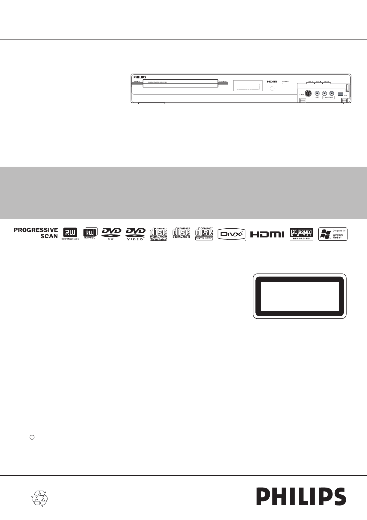
DVD Recorder DVDR3475/37
Service
Service
Service
Service
34753475
Service
Service Manual
Survey of versions:
/37 NTSC
c Copyright 2007 Philips Consumer Electronics B.V. Eindhoven, The Netherlands.
All rights reserved. No part of this publication may be reproduced, stored in a retrieval
system or transmitted, in any form or by any means, electronic, mechanical, photocopying,
or otherwise without the prior permission of Philips.
CLASS 1 LASER PRODUCT
KLASSE 1 LASER PRODUKT
KLASS 1 LASER APPARAT
CLASSE 1 PRODUIT LASER
Published by FU-KC 0710 Service AV Systems Printed in The Netherlands Subject to modification
Version 1.1
EN 3139 785 32511

IMPORTANT SAFETY NOTICE
Proper service and repair is important to the safe, reliable operation of all
Philips Equipment. The service procedures recommended by Philips and
described in this service manual are effective methods of performing
service operations. Some of these service special tools should be used
when and as recommended.
It is important to note that this service manual contains various CAUTIONS
and NOTICES which should be carefully read in order to minimize the risk
of personal injury to service personnel. The possibility exists that improper
service methods may damage the equipment. It also is important to
understand that these CAUTIONS and NOTICES ARE NOT EXHAUSTIVE.
Philips could not possibly know, evaluate and advice the service trade of all
conceivable ways in which service might be done or of the possible
hazardous consequences of each way. Consequently, Philips has not
undertaken any such broad evaluation. Accordingly, a servicer who uses a
service procedure or tool which is not recommended by Philips must first
use all precautions thoroughly so that neither his safety nor the safe
operation of the equipment will be jeopardized by the service method
selected.
TABLE OF CONTENTS
LASER BEAM SAFETY PRECAUTIONS . . . . . . . . . . . . . . . . . . . . . . . . . . . . . . . . . . . . . . . . . . . . . . . . . . . . 1-1-1
IMPORTANT SAFETY PRECAUTIONS. . . . . . . . . . . . . . . . . . . . . . . . . . . . . . . . . . . . . . . . . . . . . . . . . . . . . . 1-2-1
STANDARD NOTES FOR SERVICING . . . . . . . . . . . . . . . . . . . . . . . . . . . . . . . . . . . . . . . . . . . . . . . . . . . . . . 1-3-1
FUNCTION INDICATOR SYMBOLS . . . . . . . . . . . . . . . . . . . . . . . . . . . . . . . . . . . . . . . . . . . . . . . . . . . . . . . . 1-4-1
OPERATING CONTROLS AND FUNCTIONS. . . . . . . . . . . . . . . . . . . . . . . . . . . . . . . . . . . . . . . . . . . . . . . . . 1-5-1
SIGNAL NAME ABBREVIATIONS. . . . . . . . . . . . . . . . . . . . . . . . . . . . . . . . . . . . . . . . . . . . . . . . . . . . . . . . . . 1-6-1
CABINET DISASSEMBLY INSTRUCTIONS . . . . . . . . . . . . . . . . . . . . . . . . . . . . . . . . . . . . . . . . . . . . . . . . . . 1-7-1
HOW TO INITIALIZE THE DVD RECORDER . . . . . . . . . . . . . . . . . . . . . . . . . . . . . . . . . . . . . . . . . . . . . . . . . 1-8-1
FIRMWARE RENEWAL MODE . . . . . . . . . . . . . . . . . . . . . . . . . . . . . . . . . . . . . . . . . . . . . . . . . . . . . . . . . . . . 1-9-1
BLOCK DIAGRAMS. . . . . . . . . . . . . . . . . . . . . . . . . . . . . . . . . . . . . . . . . . . . . . . . . . . . . . . . . . . . . . . . . . . . 1-10-1
SCHEMATIC DIAGRAMS / CBA’S. . . . . . . . . . . . . . . . . . . . . . . . . . . . . . . . . . . . . . . . . . . . . . . . . . . . . . . . . 1-11-1
WAVEFORMS . . . . . . . . . . . . . . . . . . . . . . . . . . . . . . . . . . . . . . . . . . . . . . . . . . . . . . . . . . . . . . . . . . . . . . . . 1-12-1
WIRING DIAGRAM . . . . . . . . . . . . . . . . . . . . . . . . . . . . . . . . . . . . . . . . . . . . . . . . . . . . . . . . . . . . . . . . . . . . 1-13-1
SYSTEM CONTROL TIMING CHARTS. . . . . . . . . . . . . . . . . . . . . . . . . . . . . . . . . . . . . . . . . . . . . . . . . . . . . 1-14-1
IC PIN FUNCTION DESCRIPTIONS . . . . . . . . . . . . . . . . . . . . . . . . . . . . . . . . . . . . . . . . . . . . . . . . . . . . . . . 1-15-1
LEAD IDENTIFICATIONS . . . . . . . . . . . . . . . . . . . . . . . . . . . . . . . . . . . . . . . . . . . . . . . . . . . . . . . . . . . . . . . 1-16-1
ELECTRICAL PARTS LIST . . . . . . . . . . . . . . . . . . . . . . . . . . . . . . . . . . . . . . . . . . . . . . . . . . . . . . . . . . . . . . 1-17-1
EXPLODED VIEWS . . . . . . . . . . . . . . . . . . . . . . . . . . . . . . . . . . . . . . . . . . . . . . . . . . . . . . . . . . . . . . . . . . . . 1-18-1
MECHANICAL PARTS LIST . . . . . . . . . . . . . . . . . . . . . . . . . . . . . . . . . . . . . . . . . . . . . . . . . . . . . . . . . . . . . 1-19-1
REVISION LIST . . . . . . . . . . . . . . . . . . . . . . . . . . . . . . . . . . . . . . . . . . . . . . . . . . . . . . . . . . . . . . . . . . . . . . . 1-20-1
Manufactured under license from Dolby Laboratories.
“Dolby” and the double-D symbol are trademarks of Dolby Laboratories.
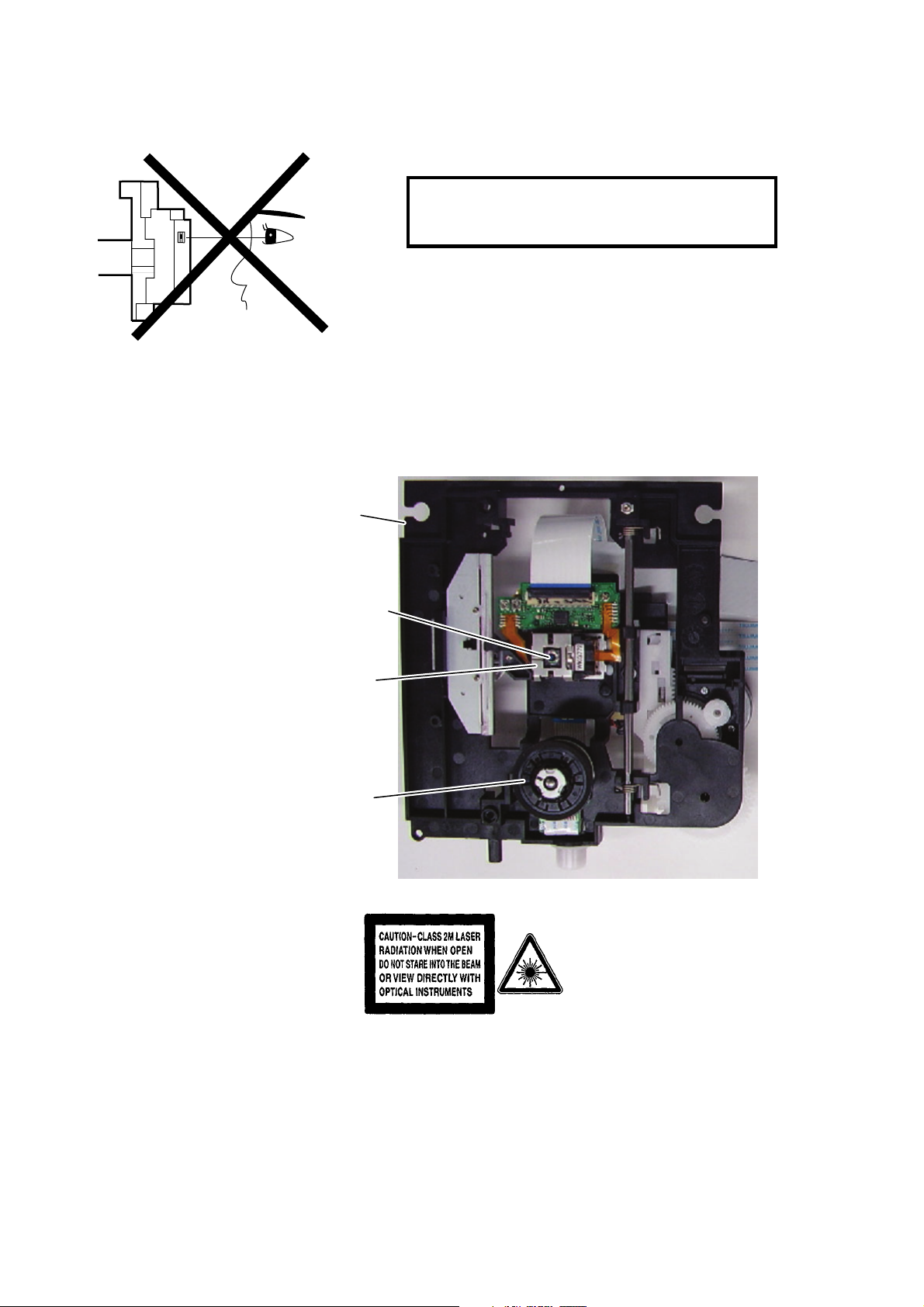
LASER BEAM SAFETY PRECAUTIONS
This DVD player uses a pickup that emits a laser beam.
Do not look directly at the laser beam coming
from the pic kup or allo w it to strike a gainst your
skin.
The laser beam is emitted from the location shown in the figure. When checking the laser diode, be sure to keep
your eyes at least 30 cm away from the pickup lens when the diode is turned on. Do not look directly at the laser
beam.
CAUTION: Use of controls and adjustments, or doing procedures other than those specified herein, may result in
hazardous radiation exposure.
Drive Mechanism Assembly
Laser Beam Radiation
Laser Pickup
Turntable
Location: Inside Top of DVD mechanism.
1-1-1 RL4NLSP

IMPORTANT SAFETY PRECAUTIONS
Product Safety Notice
Some electrical and mechanical parts have special
safety-related characterist ic s whic h ar e often not
evident from visual inspection, nor can the protection
they give necessarily be obtained by replacing them
with components rated for higher voltage, wattage,
etc. Parts that have special safety characteristics are
identified by a # on schematics and in parts lists. Use
of a substitute replacement that does not have the
same safety characteristics as the recommended
replacement part might create shock, fire, and/or other
hazards. The Product’s Safety is under review
continuously and new instructions are issued
whenever appropriate. Prior to shipment from the
factory , our products are carefully inspected to confirm
with the recognized product safety and electrical
codes of the countries in which they are to be sold.
However, in order to maintain such compliance, it is
equally important to implement the following
precautions when a set is being serviced.
Precautions during Servicing
A. Parts identified by the # symbol are critical for
safety. Replace only with part number specified.
B. In addition to safety, other parts and assemblies
are specified for conformance with regulations
applying to spurious radiation. These must also be
replaced only with specified replacements.
Examples: RF converters, RF cables, noise
blocking capacitors, and noise blocking filters, etc.
C. Use specified internal wiring. Note especially:
1) Wires covered with PVC tubing
2) Double insulated wires
3) High voltage leads
D. Use specified insulating materials for hazardous
live parts. Note especially:
1) Insulation tape
2) PVC tubing
3) Spacers
4) Insulators for transistors
E. When replacing AC primary side components
(transformers, power cord, etc.), wrap ends of
wires securely about the terminals before
soldering.
F. Observe that the wires do not contact heat
producing parts (heat sinks, oxide metal film
resistors, fusible resistors, etc.).
G. Check that replaced wires do not contact sharp
edges or pointed parts.
H. When a powe r cord ha s been re place d, chec k th at
5 - 6 kg of force in any direction will not loosen it.
I. Also check areas surrounding repaired locations.
J. Be careful that foreign objects (screws, solder
droplets, etc.) do not remain inside the set.
K. When connecting or disconnecting the internal
connectors, first, disconnect the AC plug from the
AC outlet.
1-2-1 DVDN_ISP
Safety Check after Servicing
Examine the area surrounding the repaired location for damage or deterioration. Observe that screws, parts, and
wires have been returned to their original positions. Afterwards, do the following tests and confirm the specified
values to verify compliance with safety standards.
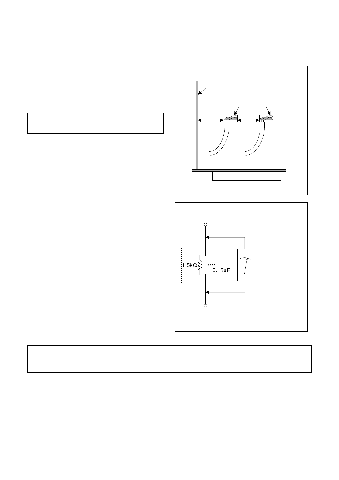
1. Clearance Distance
When replacing primary circuit components, confirm
specified clearance distance (d) and (d’) between
soldered terminals, and between terminals and
surrounding metallic parts. (See Fig. 1)
Table 1: Ratings for selected area
Chassis or Secondary Conductor
Primary Circuit
AC Line Voltage Clearance Distance (d), (d’)
120 V ≥ 3.2 mm (0.126 inches)
Note: This table is unofficial and for reference only. Be
sure to confirm the precise values.
2. Leakage Curre nt Test
Confirm the specified (or lower) leakage current
between B (earth ground, power cord plug prongs) and
externally exposed accessible parts (RF terminals,
antenna terminals, video and audio input and output
terminals, microphone jacks, earphone jacks, etc.) is
lower than or equal to the specified value in the table
below.
Measuring Method (Power ON):
Insert load Z between B (earth ground, power cord plug
prongs) and exposed accessible parts. Use an AC
voltmeter to measure across the terminals of load Z.
See Fig. 2 and the following table.
d' d
Fig. 1
Exposed Accessible Part
Z
AC V oltmeter
(High Impedance)
Earth Ground
B
Power Cord Plug Prongs
Table 2: Leakage current ratings for selected areas
AC Line Voltage Load Z Leakage Current (i) Earth Ground (B) to:
120 V
Note: This table is unofficial and for reference only. Be sure to confirm the precise values.
0.15 µF CAP. & 1.5 kΩ RES.
Connected in parallel
i ≤ 0.5 mA Peak Exposed accessible parts
1-2-2 DVDN_ISP
Fig. 2
STANDARD NOTES FOR SERVICING
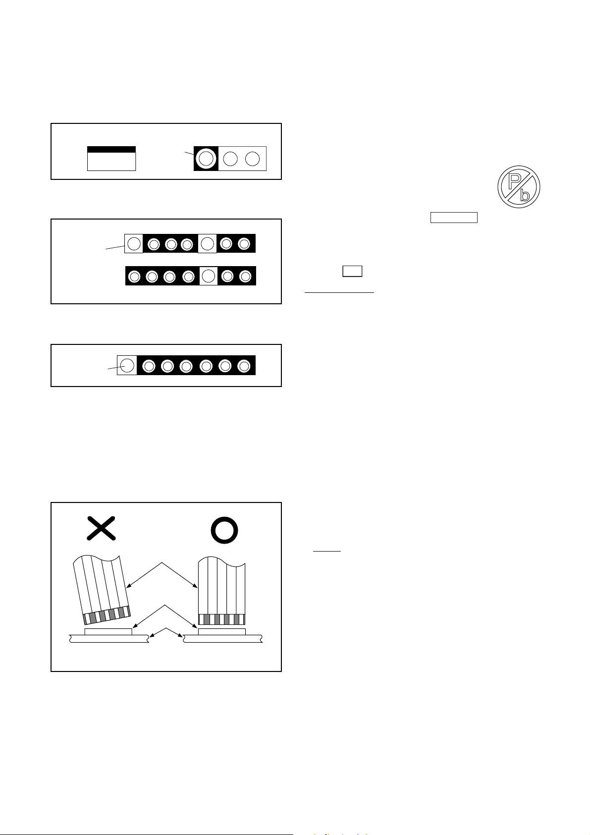
Circuit Board Indications
1. The output pin of the 3 pin Regulator ICs is
indicated as shown.
Top Vie w
Out
2. For other ICs, pin 1 and every fifth pin are
indicated as shown.
Pin 1
3. The 1st pin of every male connector is indicated as
shown.
Pin 1
Input
In
Bottom View
5
10
Instructions for Connectors
1. When you connect or disconnect the FFC (Flexible
Foil Connector) cable, be sure to first disconnect
the AC cord.
2. FFC (Flexible Foil Connector) cable should be
inserted parallel into the connector, not at an
angle.
FFC Cable
Connector
CBA
* Be careful to avoid a short circuit.
Pb (Lead) Free Solder
When soldering, be sure to use the Pb free solder.
Information about lead-free soldering
Philips CE is producing lead-free sets from 1.1.2005
onwards.
IDENTIFICATION
Regardless of special logo (not always
indicated)
One must treat all sets from
onwards, according to the next rule:
Serial Number gives a 9-digit. Digit 2&3 shows th e
WEEK, and digit 4 shows the YEAR.
So from onwards=from 1 Jan 2005 onwards
Important note: In fact also products of year 2004
must be treated in this way as long as you avoid
mixing solder-alloys (leaded/ lead- free) . So bes t to
always use SAC305 and the higher temperatures
belong to this.
Due to lead-free technology some rules have to be
respected by the workshop during a repair:
• Use only lead-free solder alloy Philips SAC305 with
order code 0622 149 00106. If lead-free solderpaste is required, please contact the manufacturer
of your solder-equipment. In general use of solderpaste within workshops should be avoided because
paste is not easy to store and to handle.
• Use only adequate solder tools applicable for leadfree solder alloy. The solder tool must be able
• To reach at least a solder-temperature of 400°C,
• To stabilize the adjusted temperature at the solder-
• To exchange solder-tips for different applications.
• Adjust your solder tool so that a temperature around
360°C
solder joint. Heating-time of the solder-joint should
not exceed ~ 4 sec. Avoid temperatures above
400°C otherwise wear-out of tips will rise drastically
and flux-fluid will be destroyed. To avoid wear-out of
tips switch off un-used equipment, or reduce heat.
• Mix of lead-free solder alloy / parts with leaded
solder alloy / parts is possible but PHILIPS
recommends strongly to avoid mixed solder alloy
types (leaded and lead-free).
If one cannot avoid or does not know whether
product is lead-free, clean carefully the solder-joint
from old solder alloy and re-solder with new solder
alloy (SAC305).
• Use only original spare-parts listed in the ServiceManuals. Not listed standard-material (commodities)
has to be purchased at external companies.
015
tip
- 380°C is reached and stabilized at the
1 Jan 2005
1-3-1 DVDN_PC_SN
• Special information for BGA-ICs:
- always use the 12nc-recognizable soldering
temperature profile of the specific BGA (for desoldering always use the lead-free temperature
profile, in case of doubt)
- lead free BGA-ICs will be delivered in so-called
'dry-packaging' (sealed pack including a silica gel
pack) to protect the IC against moisture. After
opening, dependent of MSL-level seen on indicatorlabel in the bag, the BGA-IC possibly still has to be
baked dry. (MSL=Moisture Sensitivity Level). This
will be communicated via AYS-website.
Do not re-use BGAs at all.
• For sets produced before 1.1.2005 (except products
of 2004), containing leaded solder-alloy and
components, all needed spare-parts will be available
till the end of the service-period. For repair of such
sets nothing changes.
• On our website
www.atyourservice.ce.Philips.com
information to:
• BGA-de-/soldering (+ baking instructions)
• Heating-profiles of BGAs and other ICs used in
Philips-sets
You will find this and more technical information within
the “magazine”, chapter “workshop news”.
For additional questions please contact your local
repair-helpdesk.
you find more
How to Remove / Install Flat Pack-IC
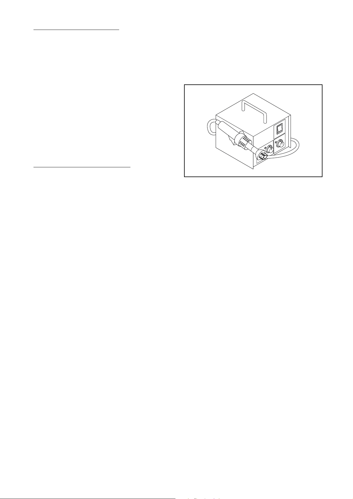
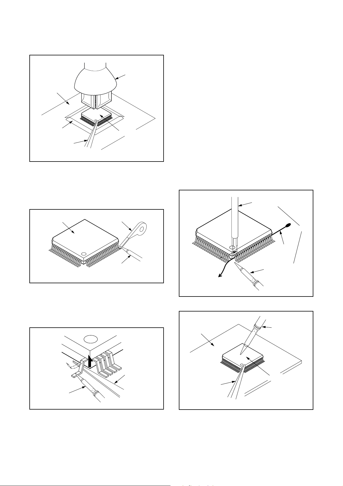
1. Removal
With Hot-Air Flat Pack-IC Desoldering Machine:
1. Prepare the hot-air flat pack-IC desoldering
machine, then apply hot air to the Flat Pack-IC
(about 5 to 6 seconds). (Fig. S-1-1)
Fig. S-1-1
2. Remove the flat pack-IC with tweezers while
applying the hot air.
3. Bottom of the flat pack-IC is fixed with glue to the
CBA; when removing entire flat pack-IC, first apply
soldering iron to center of the flat pack-IC and heat
up. Then remove (glue will be melted). (Fig. S-1-6)
4. Release the flat pack-IC from the CBA using
tweezers. (Fig. S-1-6)
CAUTION:
1. The Flat Pack-IC shape may differ by models. Use
an appropriate hot-air flat pack-IC desoldering
machine, whose shape matches that of the Flat
Pack-IC.
2. Do not supply hot air to the chip parts around the
flat pack-IC for over 6 seconds because damage
to the chip parts may occur. Put masking tape
around the flat pack-IC to protect other parts from
damage. (Fig. S-1-2)
1-3-2 DVDN_PC_SN
3. The flat pack-IC on the CBA is affixed with glue, so
be careful not to break or damage the foil of each
pin or the solder lands under the IC when
removing it.
Hot-air
Flat Pack-IC
Desoldering
CBA
Masking
Tape
Machine
Flat Pack-IC
Tweezers
Fig. S-1-2
With Soldering Iron:
1. Using desoldering braid, remove the solder from
all pins of the flat pack-IC. When you use solder
flux which is applied to all pins of the flat pack-IC,
you can remove it easily. (Fig. S-1-3)
With Iron Wire:
1. Using desoldering brai d, remove the solder from
all pins of the flat pack-IC. When you use solder
flux which is applied to all pins of the flat pack-IC,
you can remove it easily. (Fig. S-1-3)
2. Affix the wire to a workbench or solid mounting
point, as shown in Fig. S-1-5.
3. While heating the pins using a fine tip soldering
iron or hot air blower, pull up the wire as the solder
melts so as to lift the IC leads from the CBA
contact pads as shown in Fig. S-1-5.
4. Bottom of the flat pack-IC is fixed with glue to the
CBA; when removing entire flat pack-IC, first apply
soldering iron to center of the flat pack-IC and heat
up. Then remove (glue will be melted). (Fig. S-1-6)
5. Release the flat pack-IC from the CBA using
tweezers. (Fig. S-1-6)
Note: When using a soldering iron, care must be
taken to ensure that the flat pack-IC is not
being held by glue. When the flat pack-IC is
removed from the CBA, handle it gently
because it may be damaged if force is applied.
Hot Air Blower
Flat Pack-IC
Desoldering Braid
Soldering Iron
Fig. S-1-3
2. Lift each lead of the flat pack-IC upward one by
one, using a sharp pin or wire to which solder will
not adhere (iron wire). When heating the pins, use
a fine tip soldering iron or a hot air desoldering
machine. (Fig. S-1-4)
Sharp
Pin
Fine Tip
Soldering Iron
Fig. S-1-4
To Solid
Mounting Point
CBA
Tweezers
or
Iron Wire
Soldering Iron
Fig. S-1-5
Fine Tip
Soldering Iron
Flat Pack-IC
Fig. S-1-6
3. Bottom of the flat pack-IC is fixed with glue to the
CBA; when removing entire flat pack-IC, first apply
soldering iron to center of the flat pack-IC and heat
up. Then remove (glue will be melted). (Fig. S-1-6)
4. Release the flat pack-IC from the CBA using
tweezers. (Fig. S-1-6)
1-3-3 DVDN_PC_SN
2. Installation
1. Using desoldering braid, remove the solder from
the foil of each pin of the flat pack-IC on the CBA
so you can install a replacement flat pack-IC more
easily.
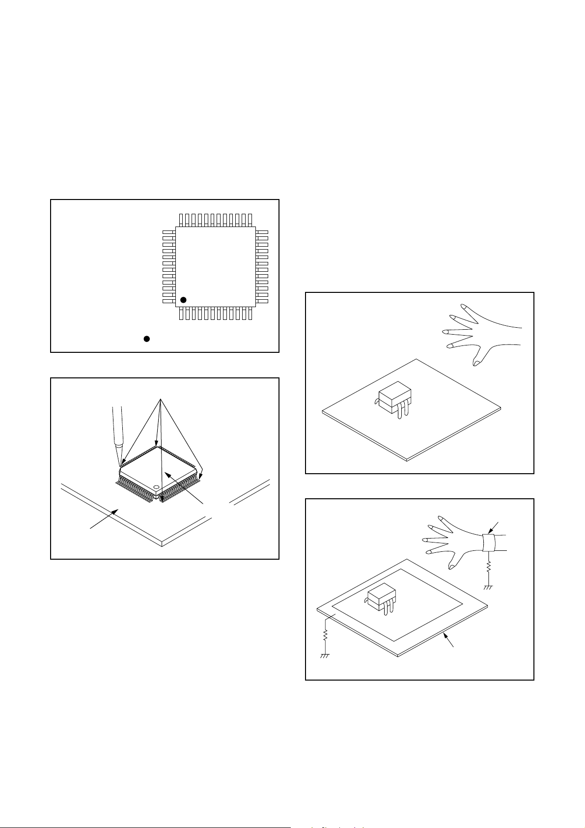
2. The “●” mark on the flat pack-IC indicates pin 1.
(See Fig. S-1-7.) Be sure this mark matches the 1
on the PCB when positioning for installation. Then
presolder the four corners of the flat pack-IC. (See
Fig. S-1-8.)
3. Solder all pins of the flat pack-IC. Be sure that
none of the pins have solder bridges.
Example :
Pin 1 of the Flat Pack-IC
is indicated by a " " mark.
Fig. S-1-7
Instructions for Handling Semiconductors
Electrostatic breakdown of the semi-cond uc tors may
occur due to a potential difference caused by
electrostatic charge during unpacking or repair work.
1. Ground for Human Body
Be sure to wear a grounding band (1 MΩ) that is
properly grounded to remove any static electricity that
may be charged on the body.
2. Ground for Workbench
Be sure to place a conductive sheet or copper plate
with proper grounding (1 MΩ) on the workbench or
other surface, where the semi-conductors are to be
placed. Because the static electricity charge on
clothing will not escape through the body grounding
band, be careful to avoid contacting semi-conductors
with your clothing.
<Incorrect>
CBA
Presolder
Flat Pack-IC
Fig. S-1-8
<Correct>
1MΩ
CBA
Grounding Band
1MΩ
CBA
Conductive Sheet or
Copper Plate
1-3-4 DVDN_PC_SN
FUNCTION INDICATOR SYMBOLS
Note: If an error occurs, a message with the error number appears on the screen.
Recording Error
Message Solution
Can not record on this disc.
This program is not allowed to
be recorded.
This disc is protected and not
recordable.
Disc is full.
(No area for new recording)
You cannot record on this disc as
Power Calibration Area is full.
Insert the recordable disc, and
ensure the disc status satisfies
the recording requiremen ts.
You cannot record copy
prohibite d programs.
Release th e disc protec t
setting in the Disc Setting
menu.
Insert the recordable disc with
enough recording space.
Error message
E35
Error
No.
1 An error occurs during data reading. 2
3
4 An error occurs with OPC. -
5 During recovery in a record. 6
7 An error occurs in a format. -
8 It cannot start an encode. 9
10
11
12
13 It is a reply that “ATAPI is not readable.” 14
15
16 An error occurs in Finalize Close. -
17 An error occurs in Rec Stop Close. 18 An error occurs in PCA Full (DVD_R). 19 Safety Stop occurs du ring editing. 20 High Speed Disc. 2
21 The disc is not formatted. 5
22 Disc Error has occurred. 3
24
25 During the Macrovision picture input. 11
26 During the CGMS picture input. 12
29 Disc Protected Disc. 6
30 No avilable recording space. 10
Error No.
Error Description Priority
There is no reply for 15 seconds in Test
Unit Read y.
Cannot write the data after trying three
times.
An error occurs ev en if recov ery has been
tried three times.
NV_PCK/RDI_PCK is not in encoded
data.
Encode Paus e co ndi tio n co ntinued for 1 0
minutes.
Encode Pause condition continued in
normal REC condition for 10 minutes.
Difference in the addres s and ca n not get
StreamID of RDI/VIDEO.
Cannot write the data after recovering
SMALL VMGI.
Cannot write the data after DVD-R
Reverse Track.
The disc except DVD-R/RW or finalized
DVD-R.
-
-
-
-
-
-
-
-
-
1
1-4-1 E7E4AFIS
Message Solution
Error
No.
Error Description Priority
You cannot record on this disc
as Power Calibration Area is
Insert a new disc. 35 PCA is Full. (in REC start) 4
full.
This disc is already finalized.
Release th e finalizin g for this
disc.
36 It is finalized. (Video Format Disc) 8
37 Access to Memory Area range outside. -
Can not record on this disc. Repeat the same operation.
38 Sector Address is wrong. 39 BUP writing error of chapter editing. -
You cannot record more than
49 titles on one disc.(The
Delete unnecessary titles. 43 Its recording capacity has been reached. 9
maximum is 49.)
You cannot record more than
254 chapters on the disc.(The
maximum is 254.)
This program is not recordable
in +VR mode.
The disc has no recording
compatibility.
Set “Make Recording
Compatible” to “ON” to conv ert
the disc.
Delete unnecessary chapter
marks.
You cannot record copy
prohibite d programs.
Set “Make Recording
Compatible” to “ON” to re write
the menu,after that y ou w ill
record to.
44 The 254 chapter has been reached. 10
45 During the CGMS picture input. 12
Trying to record onto the +VR formatting
46
disc that had been recorded by the other
recorder.
If an error occurs during the timer recording, one of the following error numbers (40 to 42) or the above error
messages (error number: 1 to 39 and 43 to 46) is displayed on the recording menu after timer recording.
(Once the screen of the program line is exited, the program line for the error will be cleared.)
(No Error Message is displayed for the error No. 40 ~ 42.)
7
A program with the error number is grayed out and asterisked on the timer programming list.
Message Solution
Error message is not
displayed.
mer Programming
Ti
z MON JAN/01 2:00AM
error number
- Set the timer programming
correctly.
- Set the timer programming
JANE30 PM PM E1
Error
No.
40
1 / 1
Error Description Priority
- Some portion has not been recorded
because of program overlapping.
- Recording did not start at th e start time.
before the start time.
Turn the power on and set the
clock correctly then set time r
41 Power failed -
programming again.
Insert the recordable disc. 42 No disc when recording -
-
1-4-2 E7E4AFIS
OPERATING CONTROLS AND FUNCTIONS
1-5-1 E7E4AIB
1-5-2 E7E4AIB
SIGNAL NAME ABBREVIATIONS
Signal Name Function
+5V-L +5V Power Supply
-FL FIP Drive Power Supply
1V2CONT +1.2V Power Supply Control Signal
AFT Tuner Voltage Input Signal
AL-30V Always -30V Power Supply
AUDIO+5V +5V Power Supply (Audio)
AUDIO+10V +10V Power Supply (Audio)
AUDIO(L)-IN Audio Signal Left Input
AUDIO(L)-OUT Audio Signal Left Output
AUDIO(R)-IN Audio Signal Right Input
AUDIO(R)-OUT Audio Signal Right Output
AUDIO-SW1 Audio Input Select Signal 1
AUDIO-SW2 Audio Input Select Signal 2
BUP+3.3V Back up +3.3V Power Sup ply
DVD-AUDIO(L) Audio Signal Left Output
DVD-AUDIO(R) Audio Signal Right Output
DVD-AUDIO-
MUTE
DVD-V DVD Video Signal
EV+2.8V +2.8V Power Supply
EV+3.3V +3.3V Power Supply
EV+5V +5V Power Supply
EV+10.5V +10.5V Power Supply
F1 Filament Power Supply 1
F2 Filament Power Supply 2
FL-DIN FL Serial Data
FL-SCL FL Serial Clock
FL-SEL FL Select (Low Level)
FL-STB FL Serial Interface Strobe
FLASH-SCL Serial Clock Signal for Flash
FLASH-SDA Serial Data Signal for Flash
FLASH-VPP Flash Writing Voltage
GND Ground
INSEL+5V Input Select +5V Power Supply
KEY-1 Key Data Input 1
KEY-2 Key Data Input 2
OUT-L Audio Signal Left Output
OUT-R Audio Signal Right Output
OUT-V Video Signal Output
P-DOWN
POFF-SELECT Power Off Select Signal
P-ON+1.8V +1.8V at Power On Signal
P-ON+3.3V +3.3V at Power On Signal
P-ON+5V +5V at Power On Signal
POW-SW Abnormal Voltage Detection
DVD Audio Mute Control Signal
Power Voltage Down Detector
Signal
Signal Name Function
PWSW Power on Signal Output
RDY
REC-LED Recording LED Control Signal
REG-CONT Power Regulator Control Signal
REG-CONT2 Power Regulator Control Signal
REMOTE Remote Signal Input
RESET Micro Controller Reset Signal
SPDIF
SUB-RXD Reception Data
SUB-SCLK Communication Clock
SUB-TXD Transmission Data
SYS-RESET System Reset Signal
VCC +3.3V Power Supply
VIDEO+5V +5V Power Supply (Video)
VIDEO-C S-Video (Chrominance) Signal
VIDEO-C-IN
VIDEO-C-OUT
VIDEO-IN1 Composite Video Signal Input
VIDEO-Pb/Cb Component Video Signal (Pb/Cb)
VIDEO-Pb/Cb-
OUT
VIDEO-Pr/Cr Component Video Signal (Pr/Cr)
VIDEO-Pr/Cr-
OUT
VIDEO-SW1 Video Input Select Signal 1
VIDEO-SW2 Video Input Select Signal 2
VIDEO-SW3 Video Input Select Signal 3
VIDEO-Y/
CVBS-IN
VIDEO-Y(I)
VIDEO-Y(I/P)
XCIN Sub Clock Input
XCOUT Sub Clock Output
XIN Main Clock Input
XOUT Main Clock Output
Ready/Busy communication
Control Signal
Digital Audio Interface Format
Signal
S-Video (Chrominance) Signal
Input
S-Video (Chrominance) Signal
Output
Component Video Signal (Pb/Cb)
Output
Component Video Signal (Pr/Cr)
Output
S-Video (Luminance) / Composite
Video Signal
S-Video (Luminance)
Signal (Interlac e)
Component Video (Luminanc e)
Signal (Interlace/P ro gress ive)
1-6-1 E7E4ASNA
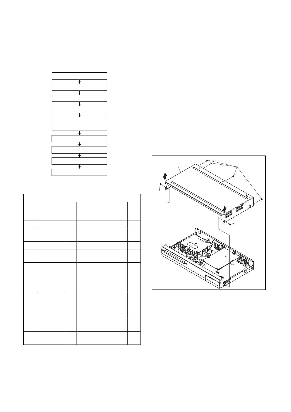
CABINET DISASSEMBLY INSTRUCTIONS
1. Disassembl y Flowchart
This flowchart indicates the disassembly steps to gain
access to item(s) t o be se rviced. Wh en re as se mbling,
follow the steps in reverse order. Bend, route, and
dress the cables as they were originally.
[1] Top Cover
[2] Front Assembly
[3] SW CBA
[4] Power SW CBA
[5] DVD Mechanism &
DVD Main CBA Assembly
[6] Power Supply CBA
[7] Rear Panel
[8] AV CBA
[9] Front Bracket
Note:
(1) Identification (location) No. of parts in the figures
(2) Name of the part
(3) Figure Number for reference
(4) Identification of parts to be removed, unhooked,
unlocked, released, unplugged, unclamped, or
desoldered.
P = Spring, L = Locking Tab, S = Screw,
CN = Connector
* = Unhook, Unlock, Release, Unplug, or Desolder
e.g. 2(S-2) = two Screws (S-2),
2(L-2) = two Locking Tabs (L-2)
(5) Refer to “Reference Notes.”
Reference Notes
1. CAUTION 1: Locking Tabs (L-1) and (L-2) are
fragile. Be careful not to break them.
[1] T op Cover
(S-1)
2. Disassembl y Method
ID/
Loc.
No.
[1] Top Cover D1 6(S-1) --[2]
[3] SW CBA D2 *2(L-3),*CN1063 --[4]
[5]
[6]
[7] Rear Panel D5
[8] AV CBA D5
[9]
↓
(1)
Part
Front
Assembly
Power SW
CBA
DVD
Mechanism
& D VD Main
CBA
Assembly
Power
Supply CBA
Front
Bracket
↓
(2)
Fig.
No.
*5(L-1), *3(L-2),
D2
*CN1061, Shield A
D2 (S-2) ---
4(S-3), (S-4), (S-5),
*CN101, *CN701,
D3
Locking Card
Spacers,
M-PCB Plate Earth
D4 4(S-6), *CN1060 ---
(S-7), 6(S-8), 2(S-9),
Fan Holder
5(S-10), DV Jack,
D V Earth Plate
2(S-11), (S-12), (S-13)
D5
M-PCB Plate Earth
↓
(3)
Removal
Remove/*Unhook/
Unlock/Release/
Unplug/Desolder
↓
(4)
(S-1)
Note
(S-1)
1
---
Fig. D1
---
---
---
↓
(5)
1-7-1 E7E4ADC
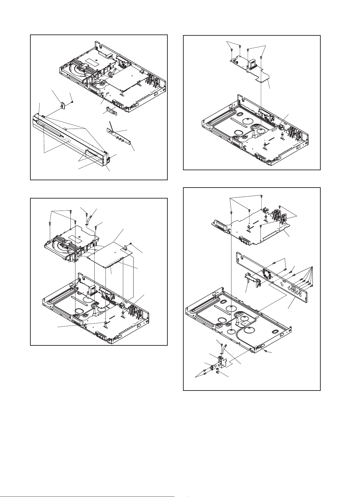
[4] Power
SW CBA
(L-1)
(S-2)
CN1061
Shield A
(S-6)
(S-6)
[6] Power
Supply CBA
CN1060
(L-2)
(S-3)
(L-1)
(L-3)
(L-2)
[2] Front Assembly
(S-4)
M-PCB Plate Earth
(S-3)
CN101
CN1063
(L-1)
[3] SW CBA
Fig. D2
[5] DVD
Mechanism
& DVD Main
CBA Assembly
(S-5)
CN701
Locking
Card
Spacer
(S-10)
Fan Holder
Fig. D4
(S-10)
[8] AV CBA
(S-9)
(S-7)
(S-8)
Locking
Card
Spacer
Fig. D3
[7] Rear Panel
(S-13)
[9] Front
Bracket
DV Jack
(S-11)
M-PCB Plate Earth
DV Earth Plate
(S-12)
Fig. D5
1-7-2 E7E4ADC
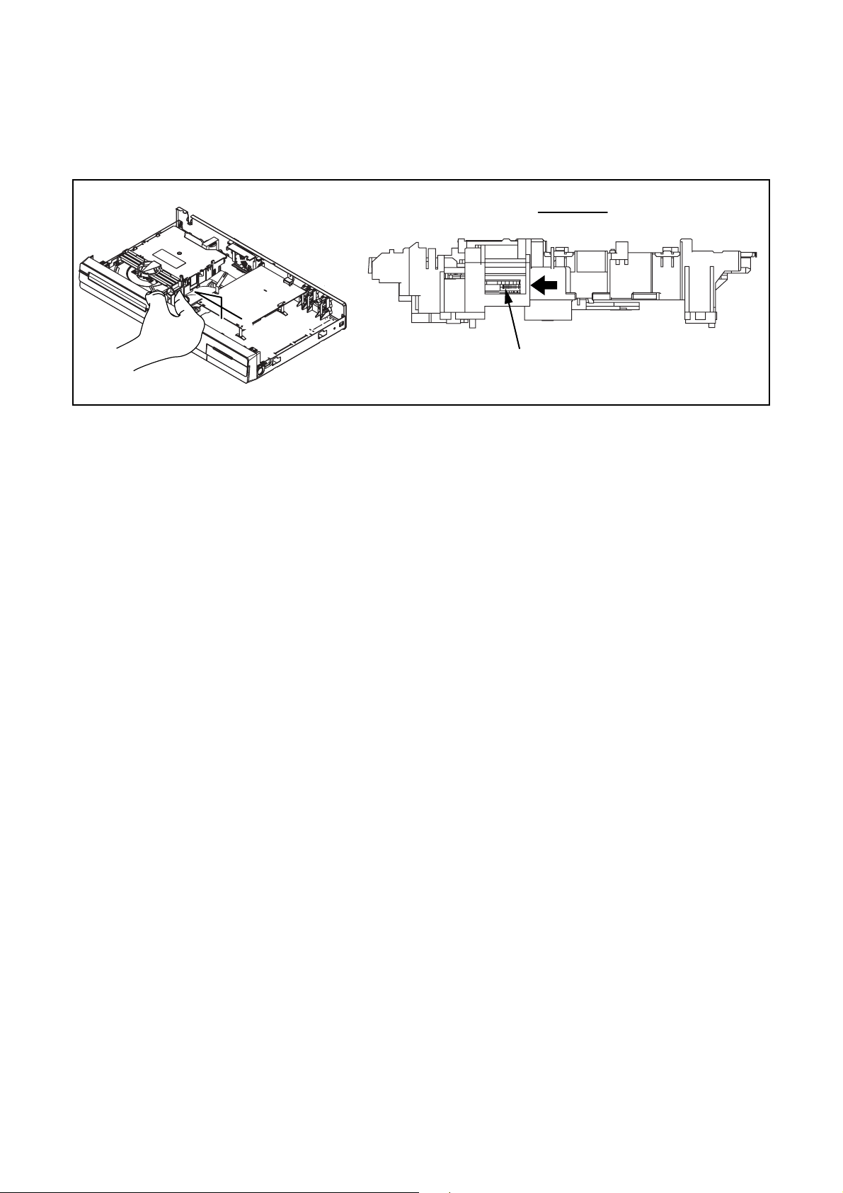
3. How to Eject Manually
Note: When rotating the gear, be careful not to damage the gear.
1. Remove the Top Cover.
2. Rotate the gear in the direction of the arrow manually as shown below until the tray descends.
3. Pull the tray out manually and remove a disc.
View for A
A
Rotate this gear in
the direction of the arrow
1-7-3 E7E4ADC

HOW TO INITIALIZE THE DVD RECORDER
To put the program back at the factory-default,
initialize the DVD recorder as the following procedure.
1. Turn the DVD recorder on.
2. Confirm that no disc is loaded or that the disc tray
is open. To put the DVD recorder into the Version
display mode, press [SKIP], [1], [2], and [3] buttons
on the remote control in the order.
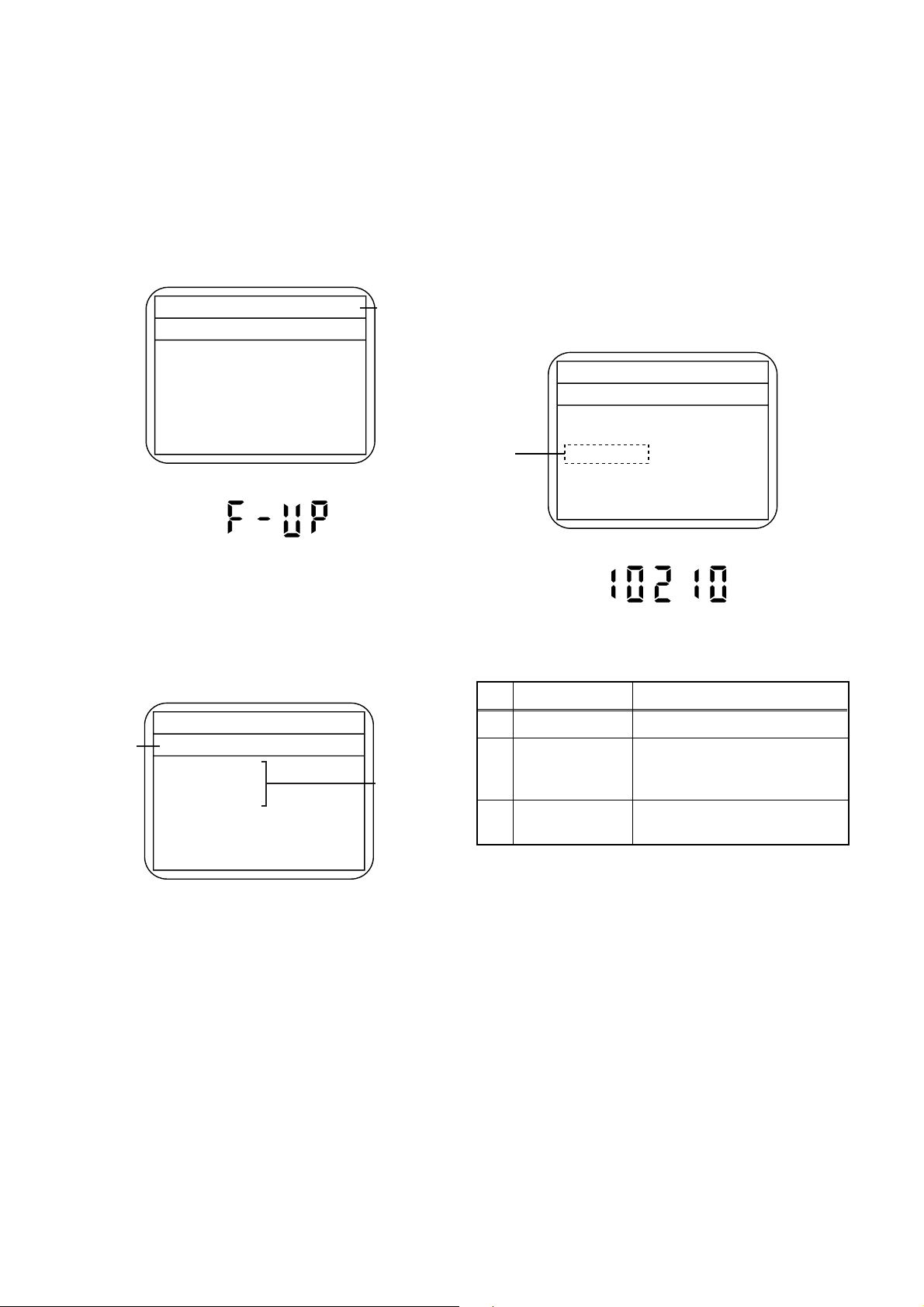
Fig. a appears on the screen.
*1: "
*2: Firmware Version differs depending on the
models, and this indication is one example.
" differs depending on the models.
*******
F/W VERSION DISP
MODEL NAME :
FE VERSION :
BE VERSION :
TT VERSION :
DV UNIQUE ID :
LD ADJUSTMENT :
DISC ADJUSTMENT :
DEFAULT SETTING : ENTER
EXIT : RETURN
*****
R40_***_***
RL4P*****S1E
T4****RDU
******** ********
OK
OK
Fig. a Version Display Mode Screen
3. Press [OK] button, then the DVD recorder starts
initializing. When the initializing is completed, the
DVD recorder exits the Version display mode and
turns off the power automatically.
* To move into the Normal mode from the
V ersion display mode, press [BACK] button on
the remote control instead of [OK] button.
* When [ ] button is pressed before [OK]
button is pressed, the DVD recorder exits the
Version display mode, then the power turns
off.
1-8-1 E7E4AINT
FIRMWARE RENEWAL MODE
1. Turn the power on and remove the disc on the tray .
2. To put the DVD recorder into version up mode,
press [SKIP], [6], [5], and [4] buttons on the remote
control unit in the order. Then the tray will open
automatically.
Fig. a appears on the screen and Fig. b appears
on the VFD.
* Firmware Version differs depending on the
models, and this indication is one example.
Firm Update Mode
Please insert a disc.
Fig. a Version Up Mode Screen
Fig. b VFD in Version Up Mode
ver. RL4P*****H1E
Current
F/W version
is displayed.
4. Select the firmware version pressing arrow
buttons, then press [OK].
Fig. d appears on the screen and Fig. e appears
on the VFD. The DVD recorder starts updating.
About VFD indication of Fig. e:
1) When Fig. d is displayed on the screen, “F-UP”
is displayed on the VFD.
2) When “Firmware Updating... XX% Complete.”
is displayed on the screen, “10210” is displayed
on the VFD.
* Firmware Version differs depending on the
models, and this indication is one example.
Firm Update Mode ver. RL4P*****H1E
(*1)
File Loading...
Fig. d Programming Mode Screen
3. Load the disc for version up.
Fig. c appears on the screen. The file on the top is
highlighted as the default.
When there is only one file to exist, Step 4 will
start automatically.
* Firmware Version differs depending on the
models, and this indication is one example.
Firm Update Mode ver. RL4P*****H1E
Disc name
is displayed.
VOL_200703250934
1 RL4P10210H1E
2 RL4P10211H1E
3 RL4P10212H1E
4 RL4P10213H1E
Fig. c Update Disc Screen
Files included
in the disc are
displayed.
1 / 1
Fig. e VFD in Programming Mode (Example)
The appearance shown in (*1) of Fig. d is
described as follows.
No. Appearance State
1 File Loading... Sending files into the memory
Firmware
2
Updating...
Writing new version data
XX% Complete.
Firmware
---
Update Failure
Failed in updating
5. After updating is finished, the tray opens
automatically.
At this time, no button is available.
6. Pull out the AC code once, then insert it again.
1-9-1 E7E4AFW
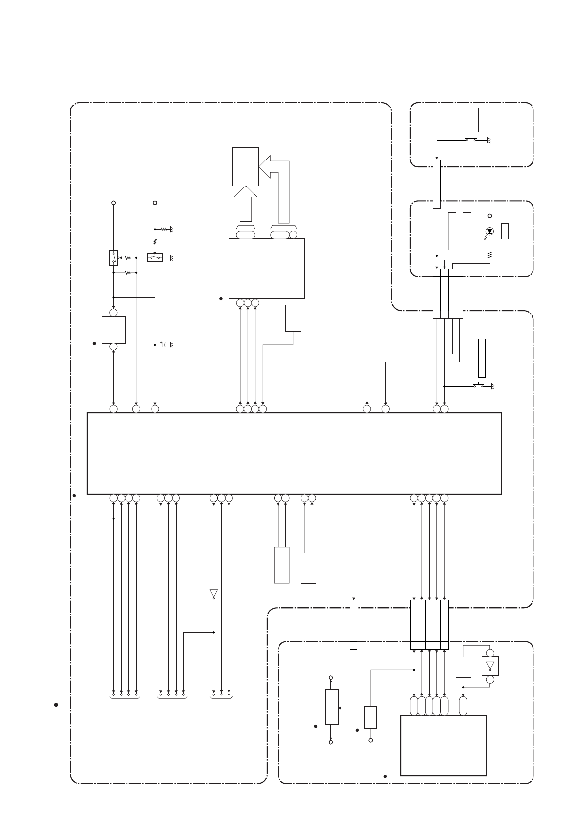
BLOCK DIAGRAMS
System Control Block Diagram
POWER
SW3010
Q1501
IC1502
EV+3.3V
RESET
1 2
14
RESET
30
P-DOWN
EV+5V
Q1502
C1501
7
VCC
(BACKUP CAPACITOR)
VFD
FL2001
GRID
~
23
17
~
7G
1G
(VFD DRIVER)
CLK
DIN
IC2001
1
28
485049
FL-DIN
FL-SCL
STB
2
27
FL-STB
REMOTE
7
a
~
~
RE2001
SEGMENT
16
14
i
h
SENSOR
REMOTE
59
REC-LED
60
POWER-LED
CN1064
2
POW-SW
2
CN1063
CN1062
3
KEY-1
3
CN1061
1
KEY-1
KEY SWITCH
2
5
6
KEY-2
REC-LED
POWER-LED
2
5
6
2
KEY-2
EV+3.3V
KEY SWITCH
OPEN/CLOSE
SW3011
REC
D1200
POWER SW CBA
“ “ = SMD
IC1501
(SUB MICRO CONTROLLER)
POW-SW
REG-CONT
3
26 REG-CONT2
52
POW-SW
REG-CONT
PWSW
REG-CONT2
TO POWER SUPPLY
BLOCK DIAGRAM
PWSW
53
VIDEO-SW1
41
42 VIDEO-SW2
43 VIDEO-SW3
VIDEO-SW1
VIDEO-SW2
VIDEO-SW3
TO VIDEO
BLOCK DIAGRAM
Q1511
POFF-SELECT
AUDIO-SW1
AUDIO-SW2
39
37 POFF-SELECT
40
AUDIO-SW1
AUDIO-SW2
POFF-SELECT
TO AUDIO
BLOCK DIAGRAM
X OUT
8
8MHz
X1501
X IN
9
RESONATOR
XC OUT
12
32.768KHz
X1502
XC IN
11
X'TAL
IC106
EV+2.8V
+1.2V
REGULATOR
111V2CONT
CN101 CN1051
IC107
RESETEV+2.8V
SUB-RXD
SYS-RESET
2219182029
CN1101
27 27SYS-RESET
30 30SUB-RXD
CN701
V25
R25
SUB-RXD
SYS-RESET
SUB-TXD
SUB-SCLK
RDY
28 28SUB-TXD
26 26SUB-SCLK
29 29RDY
B4
P22
W26
RDY
SUB-TXD
SUB-SCLK
X501
27MHz
X'TAL
L1
CLK 27 IN
AV CBA SW CBA
24
IC501
DVD MAIN CBA UNIT
1-10-1
P-ON+1.2V
IC101
(MAIN MICRO CONTROLLER)
E7E4ABLS
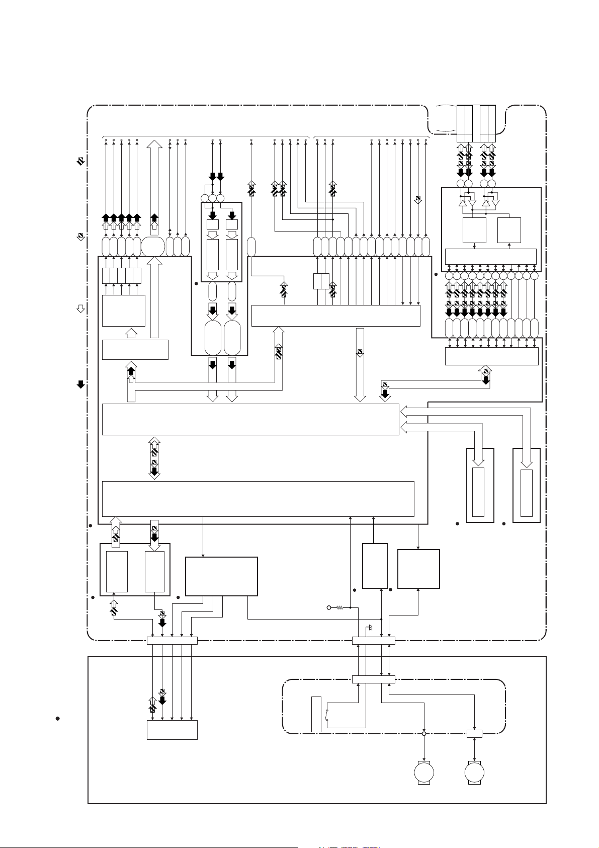
Digital Signal Process Block Diagram
VIDEO-C
VIDEO-Y(I/P)
VIDEO-Pb/Cb
J3
F2
K5
D/A
D/A
D/A
VIDEO
REC VIDEO SIGNAL PB VIDEO SIGNAL REC AUDIO SIGNAL PB AUDIO SIGNAL
VIDEO-Y(I)
VIDEO-Pr/Cr
F1
M5
A5,B5-B7
D/A
D/A
ENCODER
VIDEO
I/F
YC(0-7)
D6,D7
,C6,C7,
HDMI-SCL
HDMI-SDA
VIDEO-CLOCK
L26
U25
IIC-SCL
IIC-SDA
TO VIDEO
BLOCK
DIAGRAM
/CVBS
VIDEO-Y
10813
C5
DECODER A/D
IC701 (VIDEO DECODER)
VIDEO-CLOCK
45-50
U4,W1,W3,
VIDEO-C
A/D
DECODER
39-44
U2,U3,V1
P3,T3,T5,
Y2,AA1,AA2
PCM-DATA3
PCM-DATA0
R4
SPDIF
PCM-BCK
PCM-SCLK
PCM-LRCK
AUDIO (L)-OUT
SPDIF
AUDIO (R)-OUT
P1
D3
D1
N2
D/A
D/A
TO AUDIO
BLOCK
M1N3M2
AUDIO
I/F
DIAGRAM
MD
AIMS
E12
Y26
MC
U24
LRCK
SYSCLK
K2
M3
BCK
DATA
K1
DVD-AUDIO-MUTE
N4
T23
IC901 (IEEE1394 I/F)
DVD-AUDIO-MUTE
TO 1394
CABLE
430567
AA3
(W1)
CN901
AC2
1 TPA1P
2 TPA1N
292627
RECEIVE
Y5
AB3
4 TPB1P
DATA
DECODER
LINK
8
9
AA4
AC3
LINK
5 TPB1N
I/F
10
AE1
I/F
TRANSMIT
DATA
ENCODER
1482
11
Y4
AA5
AD1
W5
3
AC1
“ “ = SMD
(MAIN MICRO CONTROLLER)
IC101
IC201
RF/
ERROR AMP
CN201
LPC
LPC
TILT
PICK
IC301
TRACKING
-UP
FOCUS
MOTOR
DRIVER
BACK-END
DIGITAL
SIGNAL
FRONT-END
DIGITAL
SIGNAL
PROCESS
PROCESS
P-ON+3.3V
TRAY OPEN
IC202
CN301
CN1001
OP AMP
IC302
MOTOR
DRIVER
IC104 (FLASH MEMORY)
CN1002
FLASH MEMORY
DDR SDRAM
IC102 (DDR2 SDRAM)
DVD MAIN CBA UNIT
RELAY CBA
DVD MECHANISM
1-10-2
SLED
MOTOR
M
SPINDLE
MOTOR
M
E7E4ABLD
 Loading...