

Page 1
Published by KC-TE 0636 AV Systems Printed in the Netherlands Subject to modification EN 3139 785 32201
DVDR3455H
HDD + DVD Recorder
CLASS 1
LASER PRODUCT
Contents Page
1 Technical Specifications and Connection
Facilities 2
2 Safety Information, General Notes & Lead
Free Requirements 4
3 Directions for Use 6
4 Mechanical Instructions 9
5 Firmware Upgrading & Diagnostic Software 12
6 Block Diagrams,Waveforms, Wiring Diagram 15
Overall block diagram 15
Wiring diagram 16
Waveforms of Analog Board 17
Waveforms of Digital Board 18
Test Point Overview for Analog Board 19
Test Point Overview for Digital Board 20
7 Circuit Diagram and PWB Layout 21
Analog: Video Input/Output 21
Analog: Audio ADC/DAC 22
Analog: Tuner and Multi-Sound Processor
(MSP) 23
Analog: PSU and Interfaces 24
Layout: Analog-Main Part (Top View) 25
Layout: Analog-Main Part (Bottom View) 26
Front: Front Panel - Display 27
Front: Front Panel - Audio/Video-In 28
Layout: Front Panel (Top Copper Pattern)
- SMD + Components 29
Layout: Front Panel (Bottom Copper Pattern)
- Components 29
Contents Page
Front: Standby 30
Layout: Standby (Top View) 30
Digital: Back-end Processor 31
Digital: Memory 32
Digital: IEEE 1394 Physical Layer 33
Digital: Video Input Processor 34
Digital: Interfaces 35
Layout: Digital-Main Part (Top View) 36
Layout: Digital-Main Part (Bottom View) 37
Power Supply Unit: Schematic 38
Power Supply Unit: Layout 39
8 Circuit- and IC Description 41
PSU Board 41
Front Board (Panel – Display + Key) 42
Analog Board 42
Digital Board 46
IC Description 49
Analog Board 49
Digital Board 53
9 Exploded View & Spare Parts List 62
Exploded View of the set 62
Spare Parts List 63
10 Revision list 64
©
Copyright 2006 Philips Consumer Electronics B.V. Eindhoven, The Netherlands.
All rights reserved. No part of this publication may be reproduced, stored in a
retrieval system or transmitted, in any form or by any means, electronic,
mechanical, photocopying, or otherwise without the prior permission of Philips.
Version 1.1
DVDR3455H/55/75/96/97
Page 2
EN 2
1.
3139 785 3220x
Technical Specifi cations and Connection Facilities
1. Technical Specifi cations and Connection Facilities
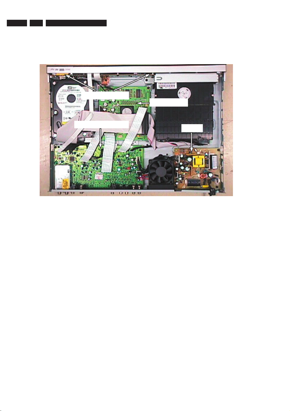
1.1 PCB Locations
Front Board
Digital Board
Analogue Board
1.2 General:
Power Supply : 127V /37
: 110V - 240V /55
: 110V /96
: 220V - 240V /75/97
Consumption : 25 W (typical)
Standby power consumption : < 3 W
1.3 RF Tuner
Test equipment: Fluke 54200 TV Signal generator
Test streams: Philips Standard test pattern
1.3.1 System
NTSC-M
1.3.2 RF - Loop Through:
Frequency range : 45 - 860 MHz
Gain: (ANT IN - ANT OUT) : ≥ -6dB
Radio Interference / max. input
voltage, at 75Ω, 3 tone method (≤
-40dB) : no limit
1.3.3 Modulator:
PSU
1.3.5 Video Performance:
Channel 25 / 503,25 MHz,
Test pattern: standard test pattern.
RF Level 74dBμV
Measured on Cinch Out
Frequency response : 0.1 - 3.58 MHz -1 ± 3dB
1.3.6 Audio Performance:
Audio Performance Analogue - HiFi:
Frequency response at Cinch (L+R)
output : 100 Hz - 10 kHz / 0 ±
3dB
S/N according to DIN 45405, 7, 1967
and PHILIPS standard test pattern
video signal : ≥ 45dB
Harmonic distortion (1 kHz, ± 25
kHz deviation) : ≤ 1.5%
1.3.7 Tuning
Automatic Search Tuning
Scanning time without antenna : typ. 3 min.
Stop level (vision carrier) : ≥ 37dBμV
Maximum tuning error during
operation : ± 100 kHz
Video Modulation : 80%±15%
Frequency response : 0 ± 3dB, 0...4.2MH
Audio Modulation 1kHz tone : ± 12kHz, tol. ± 4kHz
1.3.4 Receiver:
PLL tuning with AFC for optimum reception
Frequency range : 55 - 805 MHz
Sensitivity at 40 dB S/N : ≤ 60dBμV at 75 Ω
(video unweighted)
Manual Tuning
Manual selection in “STORE” mode
Page 3
Technical Specifi cations and Connection Facilities
3139 785 3220x
1.
EN 3
1.4 Analogue Inputs / Outputs
1.4.1 External In (Rear)
Video - Y/C (Hosiden)
according IEC 933-5
Superimposed DC-level on pin 4 (load 100k):
< 2.4V is detected as 4:3 aspect ratio
> 3.5V is detected as 16:9 aspect ratio
Input voltage Y : 1 Vpp ± 3dB
Input impedance Y : 75
Input voltage C : burst 300 mVpp ± 3dB
Input impedance C : 75
Video Cinch
Input voltage : 1 Vpp ± 3dB
Input impedance : 75
Audio Cinch
Input voltage : 2.2 Vrms max.
Input impedance : > 10k
1.4.2 Audio/Video Front Input Connectors
Audio
Input voltage : 2 Vrms max.
Input impedance : > 10k
Video - Cinch
Input voltage : 1 Vpp ± 3dB
Input impedance : 75
Video - YC (Hosiden)
according IEC 933-5
Superimposed DC-level on pin 4 (load 100 k):
< 2.4V is detected as 4:3 aspect ratio
> 3.5V is detected as 16:9 aspect ratio
Input voltage Y : 1 Vpp ± 3dB
Input impedance Y : 75
Input voltage C : burst 300 mVpp ± 3dB
Input impedance C : 75
1.4.3 Out 1
Component Video Cinch Y/Pb/Pr / Progressive Scan
according EIO-770-1-A, EIA-770-2-A
Audio - Cinch
Output voltage : 2 Vrms max
Output impedance : < 2k
1.4.4 Out 2
Video - Y/C (Hosiden)
Output voltage Y : 1 Vpp ± 3dB
C : burst 300 mVpp ± 1dB
Output impedance Y, C : 75
1.6 Audio Performance CD
1.6.1 Cinch Output Rear
Output voltage 2 channel mode : 2Vrms ± 1dB
Channel unbalance (1kHz) : <1dB
Crosstalk 1kHz : >100dB
Crosstalk 20Hz-20kHz : >87dB
Frequency response 20Hz-20kHz : ±0.2dB max
Signal to noise ratio (A-weighted) : >90dB
Dynamic range 1kHz : >83dB
Distortion and noise 1kHz : >83dB
Distortion and noise 20Hz-20kHz : >75dB
Intermodulation distortion : >70dB
Mute : >95dB
Outband attenuation: : >40dB above 30kHz
1.7 Digital Output
1.7.1 Coaxial
CDDA / LPCM : according IEC60958
MPEG1, MPEG2, AC3 audio : according IEC61937
DTS : according IEC61937
amendment 1
1.8 Digital Video Input (IEEE 1394)
1.8.1 Applicable Standards
Implementation according:
IEEE Std 1394-1995
IEC 61883 - Part 1
IEC 61883 - Part 2 SD-DVCR (02-01-1997)
Specifi cation of consumer use digital VCR’s using 6.3 mm
magnetic tape - dec. 1994
Mechanical connection according:
Annex A of 61883-1
1.9 Dimensions and Weight
Height of feet : 5.5mm
Apparatus tray closed : WxDxH:360x43x322mm
Weight without packaging : 3 kg
Weight in packaging : 4 kg
1.10 Laser Output Power & Wavelength
1.10.1 DVD
Output power during reading : 1.0mW
Output power during writing : 30mW
Wavelength : 650nm
1.10.2 CD
Output power : 1.0mW
Wavelength : 780nm
Video - Cinch
Output voltage : 1 Vpp ± 1dB
Output impedance : 75
Audio - Cinch
Output voltage : 2 Vrms max
Output impedance : < 1k
1.5 Video Performance DVD
All outputs loaded with 75 Ohm
SNR measurements over full bandwidth without weighting.
1.5.1 All Outputs
SNR : > 48dB
Bandwidth : 4.2 MHz - 3dB
1.11 Write Speed
Type of Disc (Function) Disc Rotation Speed
Read Speed CD 7X CAV (25Hz)
Read Speed DVD 4X CAV (40Hz)
Write Speed DVD+RW 2.4X ZCAV
Write Speed DVD+R 2.4X ZCAV
Page 4
EN 4
2.
3139 785 3220x
Safety Information, General Notes & Lead Free Requirements
2. Safety Information, General Notes & Lead Free Requirements
2.1 Safety Instructions
2.1.1 General Safety
Safety regulations require that during a repair:
• Connect the unit to the mains via an isolation transformer.
• Replace safety components, indicated by the symbol ,
only by components identical to the original ones. Any
other component substitution (other than original type)
may increase risk of fi re or electrical shock hazard.
Safety regulations require that after a repair, you must return
the unit in its original condition. Pay, in particular, attention to
the following points:
• Route the wires/cables correctly, and fi x them with the
mounted cable clamps.
• Check the insulation of the mains lead for external
damage.
• Check the electrical DC resistance between the mains
plug and the secondary side:
1. Unplug the mains cord, and connect a wire between
the two pins of the mains plug.
2. Set the mains switch to the ‘on’ position (keep the
mains cord unplugged!).
3. Measure the resistance value between the mains
plug and the front panel, controls, and chassis
bottom.
4. Repair or correct unit when the resistance
measurement is less than 1 M.
5. Verify this, before you return the unit to the customer/
user (ref. UL-standard no. 1492).
6. Switch the unit ‘off’, and remove the wire between the
two pins of the mains plug.
2.1.2 Laser Safety
This unit employs a laser. Only qualifi ed service personnel
may remove the cover, or attempt to service this device (due
to possible eye injury).
2.2 Warnings
2.2.1 General
• All ICs and many other semiconductors are susceptible to
electrostatic discharges (ESD, ). Careless handling
during repair can reduce life drastically. Make sure that,
during repair, you are at the same potential as the mass
of the set by a wristband with resistance. Keep
components and tools at this same potential.
Available ESD protection equipment:
– Complete kit ESD3 (small tablemat, wristband,
connection box, extension cable and earth cable)
4822 310 10671.
– Wristband tester 4822 344 13999.
• Be careful during measurements in the live voltage
section. The primary side of the power supply, including
the heatsink, carries live mains voltage when you
connect the player to the mains (even when the
player is ‘off’!). It is possible to touch copper tracks and/
or components in this unshielded primary area, when
you service the player. Service personnel must take
precautions to prevent touching this area or components
in this area. A ‘lightning stroke’ and a stripe-marked
printing on the printed wiring board, indicate the primary
side of the power supply.
• Never replace modules, or components, while the unit is
‘on’.
2.2.2 Laser
• The use of optical instruments with this product, will
increase eye hazard.
• Only qualifi ed service personnel may remove the cover or
attempt to service this device, due to possible eye injury.
• Repair handling should take place as much as possible
with a disc loaded inside the player.
• Text below is placed inside the unit, on the laser cover
shield:
Laser Device Unit
Type : Semiconductor laser
GaAlAs
Wavelength : 650 nm (DVD)
: 780 nm (VCD/CD)
Output Power : 20 mW
(DVD+RW writing)
: 0.8 mW
(DVD reading)
: 0.3 mW
(VCD/CD reading)
Beam divergence : 60 degree
CLASS 1
LASER PRODUCT
Figure 2-1
Note: Use of controls or adjustments or performance of
procedure other than those specifi ed herein, may result in
hazardous radiation exposure. Avoid direct exposure to beam.
CAUTION VISIBLE AND INVISIBLE LASER RADIATION WHEN OPEN AVOID EXPOSURE TO BEAM
ADVARSEL SYNLIG OG USYNLIG LASERSTRÅLING VED ÅBNING UNDGÅ UDSÆTTELSE FOR STRÅLING
ADVARSEL SYNLIG OG USYNLIG LASERSTRÅLING NÅR DEKSEL ÅPNES UNNGÅ EKSPONERING FOR STRÅLEN
VARNING SYNLIG OCH OSYNLIG LASERSTRÅLNING NÄR DENNA DEL ÄR ÖPPNAD BETRAKTA EJ STRÅLEN
VARO! AVATTAESSA OLET ALTTIINA NÄKYVÄLLE JA NÄKYMÄTTÖMÄLLE LASER SÄTEILYLLE. ÄLÄ KATSO SÄTEESEEN
VORSICHT SICHTBARE UND UNSICHTBARE LASERSTRAHLUNG WENN ABDECKUNG GEÖFFNET NICHT DEM STRAHL AUSSETSEN
DANGER VISIBLE AND INVISIBLE LASER RADIATION WHEN OPEN AVOID DIRECT EXPOSURE TO BEAM
ATTENTION RAYONNEMENT LASER VISIBLE ET INVISIBLE EN CAS D’OUVERTURE EXPOSITION DANGEREUSE AU FAISCEAU
Figure 2-2
2.2.3 Notes
Dolby
Manufactured under licence from Dolby Laboratories. “Dolby”,
“Pro Logic” and the double-D symbol are trademarks of Dolby
Laboratories. Confi dential Unpublished Works.
©1992-1997 Dolby Laboratories, Inc. All rights reserved.
Figure 2-3
Trusurround
TRUSURROUND, SRS and symbol (fi g 2-4) are trademarks
of SRS Labs, Inc. TRUSURROUND technology is
manufactured under licence frm SRS labs, Inc.
Figure 2-4
Page 5
Safety Information, General Notes & Lead Free Requirements
3139 785 3220x
2.
EN 5
Video Plus
“Video Plus+” and “PlusCode” are registered trademarks of
the Gemstar Development Corporation. The “Video Plus+”
system is manufactured under licence from the Gemstar
Development Corporation.
Figure 2-5
Macrovision
This product incorporates copyright protection technology that
is protected by method claims of certain U.S. patents and
other intellectual property rights owned by Macrovision
Corporation and other rights owners.
Use of this copyright protection technology must be
authorized by Macrovision Corporation, and is intended for
home and other limited viewing uses only unless otherwise
authorized by Macrovision Corporation. Reverse engineering
or disassembly is prohibited.
2.3 Lead Free Requirement
Information about Lead-free produced sets
Philips CE is starting production of lead-free sets from
1.1.2005 onwards.
INDENTIFICATION:
Regardless of special logo (not always indicated)
One must treat all sets from 1 Jan 2005 onwards, according
next rules.
Example S/N:
Due to lead-free technology some rules have to be respected by the
workshop during a repair:
• Use only lead-free solder alloy Philips SAC305 with order
code 0622 149 00106. If lead-free solder-pate is required,
please contact the manufacturer of your solder-equipment.
In general use of solder-paste within workshops should be
avoided because paste is not easy to store and to handle.
• Use only adequate solder tools applicable for lead-free
solder alloy. The solder tool must be able
o To reach at least a solder-temperature of 400°C,
o To stabilize the adjusted temperature at the solder-tip
o To exchange solder-tips for different applications.
• Adjust your solder tool so that a temperature around 360°C
– 380°C is reached and stabilized at the solder joint.
Heating-time of the solder-joint should not exceed ~ 4 sec.
Avoid temperatures above 400°C otherwise wear-out of tips
will rise drastically and fl ux-fl uid will be destroyed. To avoid
wear-out of tips switch off un-used equipment, or reduce
heat.
• Mix of lead-free solder alloy / parts with leaded solder alloy
/ parts is possible but PHILIPS recommends strongly to
avoid mixed solder alloy types (leaded and lead-free).
If one cannot avoid or does not know whether product is
lead-free, clean carefully the solder-joint from old solder
alloy and re-solder with new solder alloy (SAC305).
• Use only original spare-parts listed in the Service-Manuals.
Not listed standard-material (commodities) has to be
purchased at external companies.
• Special information for BGA-ICs:
- always use the 12nc-recognizable soldering temperature
profi le of the specifi c BGA (for de-soldering always use the
lead-free temperature profi le, in case of doubt)
- lead free BGA-ICs will be delivered in so-called ‘drypackaging’ (sealed pack including a silica gel pack) to
protect the IC against moisture. After opening, dependent
of MSL-level seen on indicator-label in the bag, the
BGA-IC possibly still has to be baked dry. (MSL=Moisture
Sensitivity Level). This will be communicated via AYSwebsite.
Do not re-use BGAs at all.
• For sets produced before 1.1.2005 (except products of
2004), containing leaded solder-alloy and components,
all needed spare-parts will be available till the end of the
service-period. For repair of such sets nothing changes.
Bottom line of typeplate gives a 14-digit S/N. Digit 5&6 is the year, digit 7&8 is
the week number, so in this case 1991 wk 18
So from 0501 onwards = from 1 Jan 2005 onwards
Important note: In fact also products of year 2004 must be treated in this way as long as you
avoid mixing solder-alloys (leaded/ lead-free). So best to always use SAC305 and the higher
temperatures belong to this.
• On our website www.atyourservice.ce.Philips.com you
BGA-de-/soldering (+ baking instructions)
Heating-profi les of BGAs and other ICs used in Philips-sets
You will fi nd this and more technical information within the
For additional questions please contact your local repair-helpdesk.
fi nd more information to:
“magazine”, chapter “workshop news”.
Page 6
EN 6
R
Y
P
B
P
R
COMPONENT
VIDEO
VIDEO
(
CVBS
)
S-VIDEO
(
Y/C
)
AUDIO
COAXIAL
R
L
OUT 3
(DIGITAL AUDIO)
OUTPUT
OUT 2
OUT 1
3.
3139 785 3220x Directions For Use
3. Directions For Use
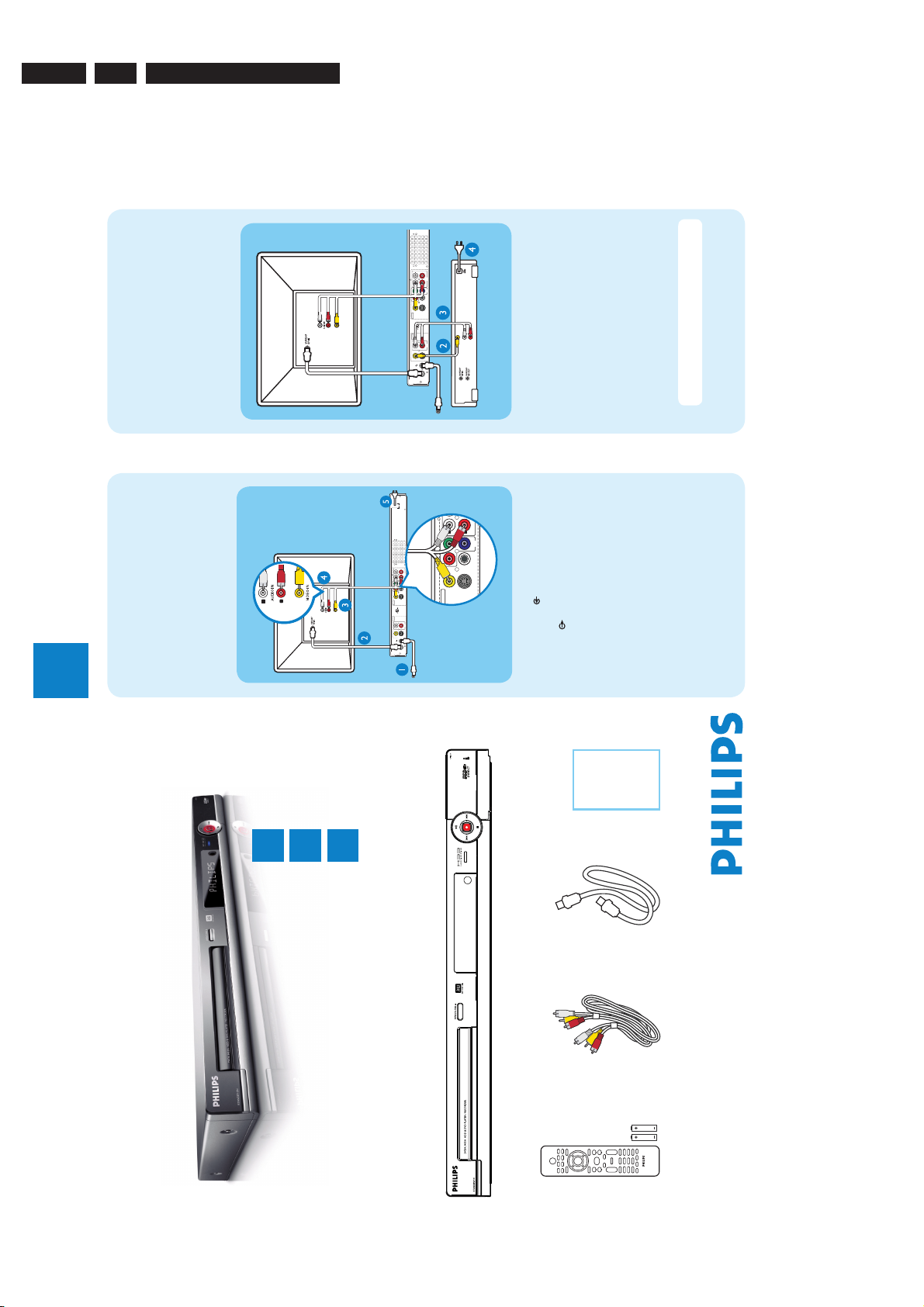
The following except of the Quick Use Guide serves as an introduction to the set.
The Complete Direction for the Use can be downloaded in different languages from the internet site of Philips Customer care Center:
www.p4c.philips.com
To AC
power
L
R
AUDIO
Philips recorder
(rear)
L
R
PR
Y
B
P
OUT 3
VIDEO
COMPONENT
COAXIAL
PR
(DIGITAL AUDIO)
)
)
Y/C
(
CVBS
(
VIDEO
To
~
MAINS
OUT 1
OUT 2
OUTPUT
R
LISTED
1040.10 and 1040.11
DVD RECORDER 22F8
Complies with 21 CFR
INPUT
L
R
)
CVBS
(
VIDEO
EXT 1
ANTENNA-IN
TV-OUT
antenna
or set-
S-VIDEO
AUDIO
)
Y/C
(
S-VIDEO
EXT 2
top box
OUT
VIDEO
L
R
OUT
AUDIO
VCR or similar device
‘Basic Connections’ to connect the recorder
before you proceed to step 2 below.
connect the VIDEO (CVBS) EXT 1 jack on
this recorder to the yellow VIDEO OUT jack on
(rear)
A Follow the steps 1 to 5 of ‘Connecting’ under
the VCR.
B Use a yellow video cable (not supplied) to
C Use another red and white audio cable (not
jacks on this recorder to the red and white
AUDIO OUT jacks on the VCR.
supplied) to connect the AUDIO L/R INPUT
AC power outlet.
programs.
Note In this setup, the VCR cannot record TV
D Connect the power cable from your VCR to an
For additional connection diagrams, see the
accompanying User Manual.
Television (rear)
Before Connecting
Connection with a VCR
or similar device
A
Your new Philips recorder replaces the VCR for your
Connecting
recording needs. First, unplug all the connections from
your VCR.
B
To AC
power
Television (rear)
L
R
R
Start with the ‘Basic Connection.’
If you have a VCR, follow the instructions for ‘Connection with a VCR or similar device’.
Connect
1
Before Connecting
Basic Connection
A
Unplug the antenna cable that is currently connected
to your TV.
Connecting
B
Connect
1
Enjoy
Set up
2
3
L
R
AUDIO
L
R
P
R
Y
B
Philips recorder
(rear)
P
OUT 3
VIDEO
COMPONENT
R
COAXIAL
P
(DIGITAL AUDIO)
)
)
Y/C
(
CVBS
(
VIDEO
S-VIDEO
OUT 1
OUT 2
OUTPUT
R
LISTED
1040.10 and 1040.11
DVD RECORDER 22F8
Complies with 21 CFR
INPUT
L
R
AUDIO
)
)
Y/C
(
CVBS
(
VIDEO
S-VIDEO
EXT 2
EXT 1
ANTENNA-IN
TV-OUT
To antenna
or set-top box
jack on this recorder to the VIDEO IN jack on
Antenna In jack on the TV.
ANTENNA-IN jack on the recorder.
TV-OUT jack on this recorder to the
A Connect the antenna cable to the
B Use the supplied RF coaxial cable to connect the
the TV.
to connect the VIDEO (CVBS) – OUT1
C Use the supplied audio/video cable (yellow plug)
User
plugs) to connect the AUDIO L/R OUTPUT
jack on this recorder to the AUDIO IN jacks on
the TV.
D Use the supplied audio/video cable (red/ white
Manual
an AC power outlet.
E Connect the power cable from the recorder to
RF Coaxial Cable
HDD & DVD Player/ Recorder DVDR3455H
Quick Start Guide
What’s in the box?
HDD & DVD Player/ Recorder
Audio/Video Cable
and 2 batteries
Remote Control
Page 7
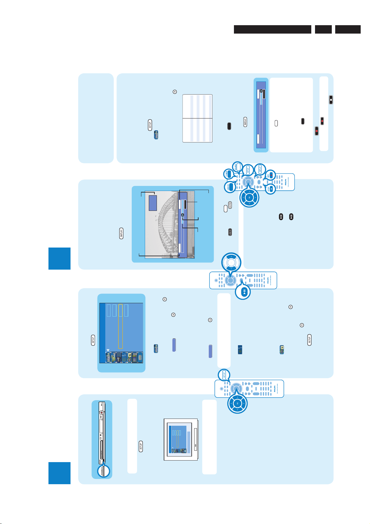
Before recording to hard disk
Start Recording
A
You can preset the recording quality for content
Instant Replay
While watching a live TV program, you can press left
W to jump back 10 seconds upon every single press for
instant replay.
To return to live broadcast, press and hold right X.
recorded to the time shift buffer.
Directions For Use
{ Record Quality } and press right X.
Press down T repeatedly until you highlight
A Press SETUP on the remote control.
B Highlight and press right X .
confirm.
mode of recording quality and press OK to
C Use up S / down T keys to select the preferred
346885
160GB Hard Disk
that can be stored
Hours of Recording
Record Quality
HQ High Quality
SP Standard Play
SPP Standard Play Plus
102
LP Long Play
136
EP Extended Play
200
270
SLP Super Long Play
SEP Super Extended Play
Values are estimates only. Parts of the HDD storage will be
reserved for the operations of this recorder and time shifting.
Record to hard disk
B
3139 785 3220x
09:15:36 AM
to go to the TV program
CH + / -
A Press TUNER to switch to tuner mode.
B Press
03:15:36 AM
channel you wish to record.
video bar.
C Press DISPLAY to display the time shift
LIVE
to record from a DV
press SOURCE repeatedly to cycle through
video input sources from:
{ CAM 1 } : VIDEO jack on the front
Note To record from a connected external device,
camcorder connected via the DV IN jack on the
{ CAM 2 } : S-VIDEO jack on the front
recorder.
{ EXT 1 } : VIDEO (CVBS) EXT1 jack on the back
{ EXT 2 } : S-VIDEO (Y/C) EXT2 jack on the back
or Press USB/DV
3.
EN 7
minutes increments per single press.
Note Press REC repeatedly to extend 30
D Press REC to start recording.
E To stop recording, press STOP .
Enjoy
3
CH003
Shows TV channel or
video input source
Start time
of program
About the Time Shift Buffer
(TSB)
Once you switch on this recorder, the currently
selected TV program will be stored in a temporary
storage called the ‘TSB’ (Time Shift Buffer). The TSB
can store up to 6 hours of recordings temporarily.
SP
5min.
Record Quality
Auto Chapter Marker
SETUP MENU - GENERAL
Initial Installation
B
A Press SETUP on the remote control.
(The TSB in playback mode)
Shift video bar.
Press DISPLAY once to display the Time
Search
Edit
Auto Program
Manual Program
Setup and install TV channels.
B
Press down T repeatedly until you highlight
Highlight and press right X .
{ Auto Program - Search } and press OK .
time
09:15:36 AM
08:30:45 AM
03:15:36 AM
to proceed.
and press OK
OK
OK
Highlight { Tuner Input Source }, press
right X and select a suitable setting:
Select
A warning message will appear.
Current
Time of current
screen playback
TSB
status icon
in playback
Program stored
in TSB
and press OK to start
OK
CONTINUE
Select
cable/satellite box.
to the antenna wall outlet.
{ Cable } – if the recorder is connected via a
{ Air } – if the recorder is connected directly
.
USB/DV , DVD REC
another mode: SOURCE ,
once you press CH + / - or if you switch to
Pause ‘live’ TV
At times, you may be interrupted while
watching your favourite program. Now you can
PAUSE it, as if you were in control of the
broadcast.
The contents on the time shift buffer will be erased
PAUSE LIVE TV
automatic TV channel search.
Select the language.
Highlight and press right X .
disc playback.
antenna connection and start the channel search
again.
Note If no channels were found, check the
C
playback.
– select the System Language
– select the Audio Language for DVD
– select the Subtitle Language for DVD disc
A Press PAUSE LIVE TV while
Set the date and time
playback.
Highlight and press right X.
– select the Disc Menu Language for DVD disc
D
watching any live TV program to suspend it.
right X.
B Press PAUSE LIVE TV to continue.
C To return to live broadcast, press and hold
To jump forward playback, press right X once for
every 30 seconds.
to con rm.
Your Philips recorder is now ready for use!
Press SETUP to finish the installation.
date/time, then press OK
E
Select { Date (dd/mm/yy) } or
{ Time (hh:mm:ss) } and press OK .
Use the numeric keypad 0 - 9 to input the
Set up
2
Philips recorder (front panel)
Finding the viewing channel
switched off or in standby mode before proceeding.
A
Note If connected to your VCR, make sure it is
A Press STANDBY-ON on the recorder
B Turn on the TV.
Search
SP
5min.
Edit
Record Quality
AutoChapter Marker
Auto Program
Manual Program
SETUP MENU - GENERAL
To exit, press [SETUP].
the Channel Down button repeatedly until you see
the { SETUP MENU - GENERAL } page. This is
C Press SETUP .
the correct viewing channel for the recorder.
D Press ‘0’ on the TV’s remote control, then press
the TV’s remote control (if available) to select the
correct viewing channel. See your TV’s user manual.
Note You may press the AV or SELECT button on
Page 8
EN 8
3.
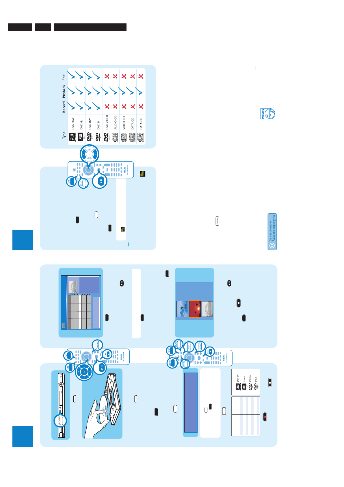
Types of discs used on this
3139 785 3220x
recorder
PAUSE LIVE TV
Directions For Use
2006 © Koninklijke Philips N.V.
All rights reserved.
12 NC 3139 245 24611
Enjoy
3
Copying to a DVD
recordable disc
You can copy the contents in your hard disk to a DVD
HDD 10 Titles
the hard disk.
recordable disc.
A Insert a recordable DVD disc.
B Press HDD to view the titles on
C Use up S or down T keys to select
00:20:20
SP NTSC
1. Press [SELECT] to
mark or unmark
recordings.
2. Press [HDD] to
copy selected
recordings to DVD.
Drama
Travel
News
News
News
Nature
Title 3
Titl e
Date Time
Ch.
No
02.00 PM
05/20/06
001 CH001
04.00 PM
08.30 PM
05/14/06
04/25/06
CH003
CH009
002
003
08.30 PM
03.30 PM
04/30/06
03/28/06
CH008
CH002
004
005
09.30 PM
11.00 AM
04/12/06
07/04/06
CH008
CH002
006
007
Discover
10.30 PM
07/23/06
CH011
008
For other options, press [DVD], [DV],
D Press SELECT to mark the
Press[SHUFFLE] to
sort by title.
[TUNER] keys. Press [RIGHT] to go to
edit menu.
titles you wish to copy.
the title.
Playback from hard disk
Start playback
A
PAUSE LIVE TV
HDD to start copying to the
recordable DVD disc.
E Once you finish your selection, press
disk.
A Press HDD to view the titles on the hard
TV programs in tuner mode or select
another HDD title for playback.
icon will be shown on the screen.
Note When copying is in progress, the
F During copying, you can continue watching
playback.
B Use up S or down T keys to select the title.
C Highlight the title you want and press to start
will no longer be shown.
G Once the copying process completes, the icon
anytime.
Note To access the edit menu, highlight the title
and press right X.
D Press HDD to go back to the HDD menu
1. Sports
11 / 05 / 2006
12 : 31 : 53 PM
SP 00 : 03 : 00
Playback from a disc
to view the list of titles on the disc.
If the disc menu does not show, press DVD
B
A Insert a CD or DVD disc.
Need help?
3. My movie
05 / 08 / 2006
2. Nature
09 / 07 / 2006
03 : 30 : 45 PM
SPP 00 : 05 : 59
Empty
on the remote control for onscreen helptext when using your Philips recorder.
DISPLAY
Onscreen Helptext
Press
User Manual
09 : 31 : 53 PM
SP 00 : 06 : 45
list of options and/or titles.
B Use up S or down T keys to scroll through the
See the user manual that came with your Philips recorder.
Online
Go to www.philips.com/support.
anytime.
playback.
C Highlight the title you want and press to start
D To stop, press STOP .
E Press DVD to go back to the disc menu
accompanying User Manual.
For more recording and playback options, see the
Enjoy
3
Philips recorder (front panel)
of the recorder.
Inserting discs
A Press OPEN/CLOSEç on the front
to go to the TV program
CH + / -
Record to a DVD recordable disc
tray.
facing up.
B Get a DVD disc and place in the tray with the label
C Press OPEN/CLOSEç again to close the
channel you wish to record.
C
A Press TUNER to switch to tuner mode.
B Press
C Insert a recordable DVD disc.
Record to Optical Disc As Standard Play
System State: Stop
mode and display the information bar.
Press DVD REC to switch to direct record
Types of discs for recording
to record from a DV
Elapsed Time: 00:00:00 Remaining Time: 02:00:00
camcorder connected via the DV IN jack on the
press SOURCE repeatedly
recorder.
Note To record from a connected external device,
OR press USB/DV
4.7 GB
that can be stored
Hours of Recording
Record Quality
preferred mode of recording quality.
D Press SELECT repeatedly to select the
1
2
2.5
DVD±R/±RW disc
High Quality HQ
Standard Play SP
Standard Play Plus SPP
346
Long Play LP
Extended Play EP
Super Long Play SLP
8
Super Extended Play SEP
E Press REC to start recording.
F To stop the recording, press STOP .
Page 9
Mechanical Instructions
4. Mechanical Instructions
Note : The position numbers given here refers to the Exploded view
on chapter 9
3139 785 3220x
4.
EN 9
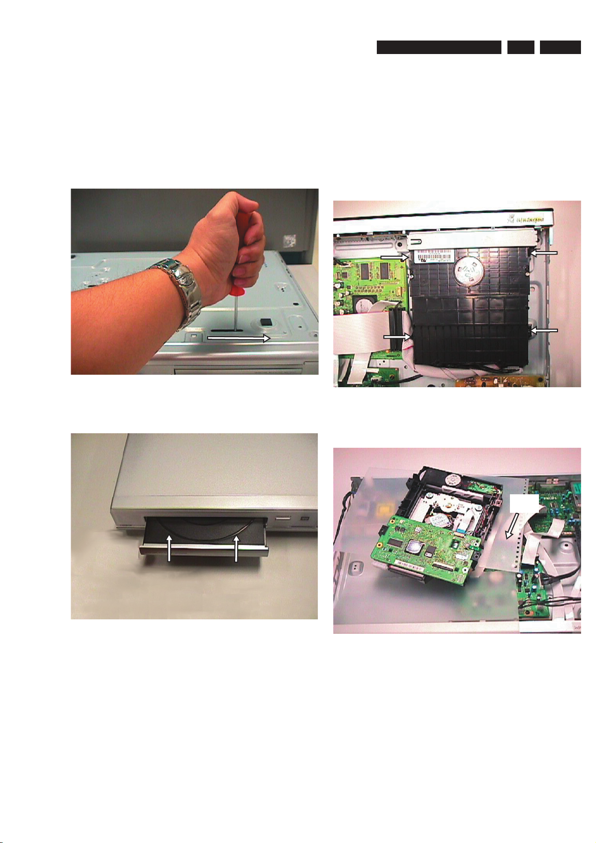
4.1 Dismantling of the DVD Tray Cover manually
1) Insert a screw-driver into the slot provided at the bottom
of the set and push in the direction as shown in Figure 4-1
to unlock before sliding the loader 1001 out.
Figure 4-1: Slide out Cover Tray
2) Remove the Cover Tray 110 as shown in Figure 4-2.
4.2 Dismantling of the Basic Engine (Drive D4.5
open)
1) Remove 7 screws to loosen Top cover 240 .
2) Remove 4 screws to loosen the Basic Engine assembly
1001 as shown in Figure 4-3.
Figure 4-3: Remove Basic Engine
3) Basic Engine Service position as shown in Figure 4-4.
Figure 4-2: Remove Cover Tray
Insulation
Sheet
Figure 4-4: Basic Engine Service Position
Page 10
EN 10
4.
3139 785 3220x
Mechanical Instructions
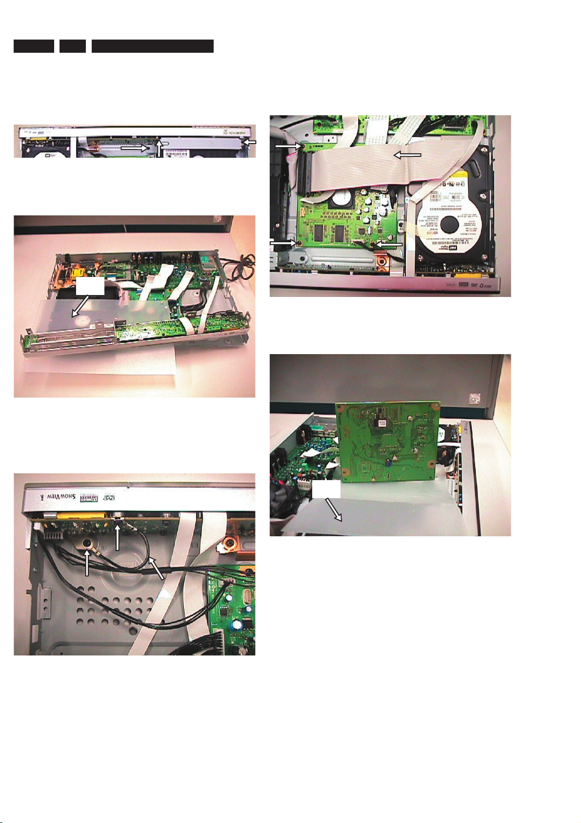
4.3 Dismantling of Frontboard
1) Remove Screws as indicated to detach plate front loader
182 from Frame assembly 0920 as shown in Figure 4-5
and also secure Front PCB .
Figure 4-5: Detach Front Panel
2) Service Position of Frontboard as shown in Figure 4-6.
Insulation
Sheet
4.4 Dismantling of the Digital Board
1) Remove 4 screws to loosen the Digital Board 1013 as
shown in Figure 4-8.
Figure 4-8: Remove Digital Board Mounting screw
2) Service Position for Digital Board is given in Figure 4-9.
Figure 4-6: Frontboard Service Position
Note: When Assembling back the Frontboard ,please remember
to screw the Board ground connector to the chasis ground for
ESD issue as show in Figure 4-7.
Figure 4-7: FrontBoard ground to Frame Ground
Insulation
Sheet
Figure 4-9: Digital Board Service Position
Page 11
Mechanical Instructions
3139 785 3220x
4.
EN 11
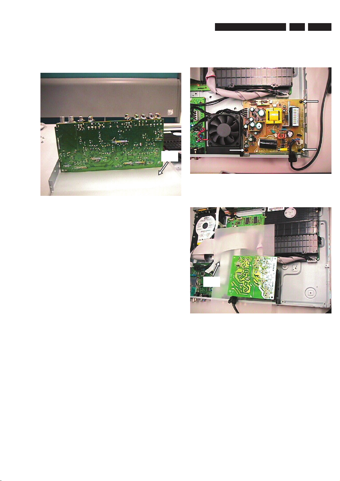
4.5 Dismantling of the Analogue Board
1) Remove screws from the rear panel 230 to detach
Analogue Board.
2) Service Position of Analogue Board is given in Figure 4-10.
Figure 4-10: Analogue Board Service Position
Insulation
Sheet
4.6 Dismantling of the PSU Board
1) Remove 3 screws to loosen the PSU Board 1002 as
shown in Figure 4-11.
Figure 4-11: Remove mounting screw of PSU
2) Service position for PSU Board is given in Figure 4-12.
Insulation
Sheet
Figure 4-12: PSU Board Service Position
Page 12

EN 12
5.
3139 785 3220x
Firmware Upgrading & Diagnostic Software
5. Firmware Upgrading & Diagnostic Software
5.1 Firmware Upgrading
A. Preparation to upgrade fi rmware:
1. Unzip the zip-archive fi le
2. Start the CD Burning software and create a new CD project (data disc) with the following settings:
File system: Joliet
Format: MODE 2: CDROM XA
Recording mode: SINGLE SESSION (TRACK-AT-ONCE), FINALIZED CD
Note: Long fi le name is necessary for the preparation of the upgrade disc
3. Place the content of the zip-archive into the root directory of the new CD project.
4. Burn the data onto a blank CDR or CD-RW
B. Procedure to apply the fi rmware upgrade:
1. Open the tray and load the Upgrade CDROM.
2. The tray closes and set will display:
“FLASH1”
3. The OSD will display
“Software Upgrade Disc detected. Select OK to start upgrading or CANCEL to exit.”
4. Click on the <OK> button.
5. The set will display:
“Upgrading Software . Please Wait . Do not switch off the power . ”
It will do the Upgrade for the loader and OSD will show .
“Loader Software Upgrade
Loader Software Upgrading . Please Wait .Do not switch off the power.”
The whole process takes less than 5 minutes
Note: Do not press any button or interrupt the mains supply during the upgrading process, otherwise the set may becomes defective
6. When the upgrade is completed the tray will open automatically and the set will display:
“Loader Upgrade process has completed successfully . Press <OK> to reboot system.”
7. The tray open and the set will display:
“DRV OK”
8. Press <OK> and the set goes to standby .
*Note : 1) The content of the HDD(i.e. the video recording(s) and/or mp3 fi le(s)) will not be erased during the fi rmware
upgrading process.
Page 13

5.
Firmware Upgrading & Diagnostic Software
3139 785 3220x
EN 13
5.2 Preparations for new HDD
If the defects is due to a faulty HDD, steps must be taken to replace the set with a new HDD . The
procedure below show the steps taken to prepare a new HDD for use on the set.
1. Replace the Faulty HDD with a new HDD.
2. Before connecting the new HDD on the Digital Board ,the jumper pin at the connector of the HDD is to be removed.
3. Connect the new HDD to the Digital Board.
4. Power up the set . It will open the tray and prompt to load the upgrading disc.(the upgrade disc is
the same disc under fi rmware upgrading.)
5. The set will display
“Load”.
6. Put the upgrade disc and close the tray and the set will show
“Copy” ……… “Boot”
7. The rest of the procedure follows the software upgrade given in 1B -Procedure to apply the fi rmware upgrade.
*Note :1) Do not press any button or interrupt the main supply, otherwise the set may become defective.
2) When the HDD formatting is successful, the set will go to standby mode.
5.3 Verifi cation of Firmware
How to read out the fi rmware version to confi rm set has been upgraded:
1. Power up the set
2. Press <setup> <3> <2> <1> in the correct sequence
3. Press <select> button
4. The TV connected to the set will display:
BUILD :B5019V04/Date:May 10 2006
Loader Version : 45.04.05.04
Macrovision Version :
MPEG Chip ID:
Audio DAC:
Region Num:1
Developer:Philips PS3455H 55 R19.04
YesDVD Version :YR.2.1.2.30306
5. Press <Setup> button to exit.
Page 14

EN 14
Notes:
5.
3139 785 3220x
Firmware Upgrading & Diagnostic Software
Page 15
EN 15
3139 785 3220x
6.
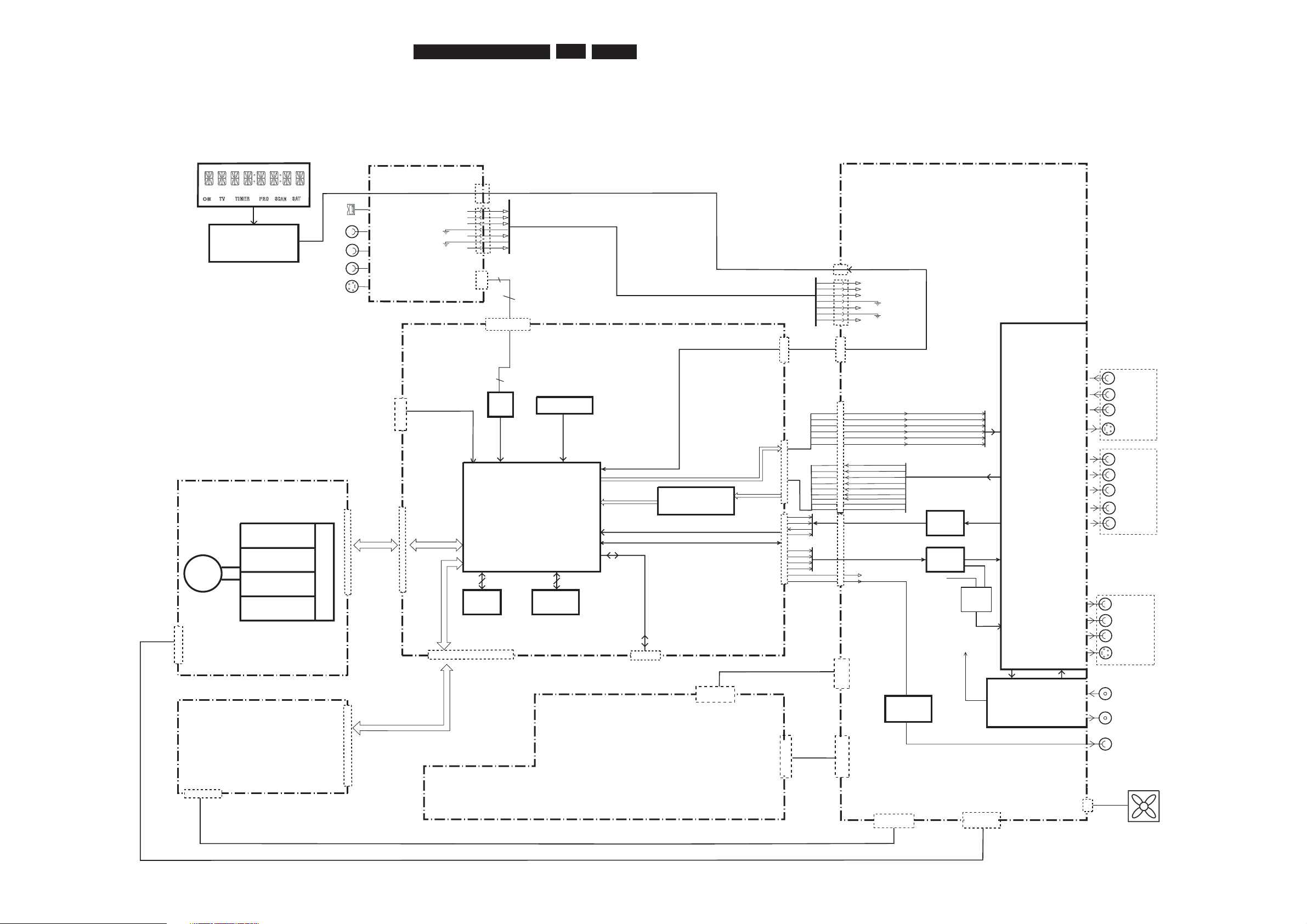
6. Block Diagrams, Waveforms, Wiring Diagram
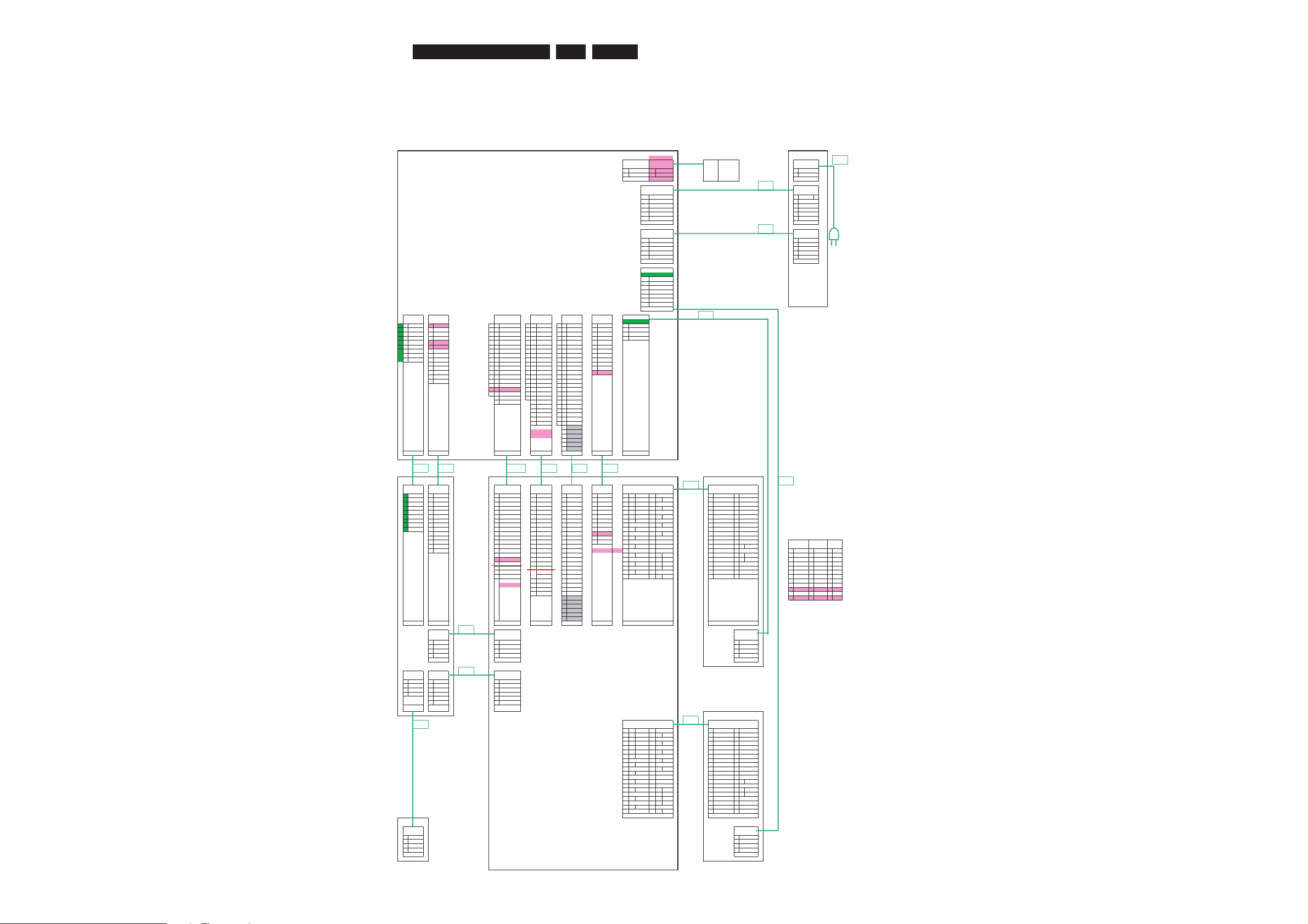
Block Diagrams, Waveforms, Wiring Diagram.
Overall Block Diagram of the Set
Front Keyboards
AUDIO PCM I2S
AUD_BCKI
AUD_WCKI
AUD_DAT(0))
AUD_SPDIF0
AUDIO ENCODER I2S
ANALOG AUDIO / VIDEO
D_CVBS
D_Y
D_C
D_VR
VOA_GY
VOA_BPb
VIA_GY Br
VIA_BPb
VIA_RPr
VIA_SC_FR
TUNER
INPUT/OUTPUT
PROCESSING &
SOURCE
SELECTION
ANALOG BOARD
2
1
AR
AL
CVBSFIN
CFIN
YFIN
3
4
5
7
9
1300
1201
1102
1205
1600
1536
S-VIDEO
CVBS
AUDIO R
AUDIO L
AINFR
AINFL
CVBSFIN
CFIN
YFIN
ADC
7
9
11
12
13
14
15
12
14
16
18
20
22
DDRAM
FLASH
VIDEO INPUT
PROCESSING
DIGITAL AUDIO
RS2321671
SERVICE
1111
1522
1551
DIG.VIDEO
2
3
5
16
7
18
1
3
5
7
9
S-VIDEO
CVBS
RF IN - ANTENNA
RF OUT - TV
PHY
DIGITAL AUDIO OUT
DOMINO DMN-8652
MPEG 2, AC3 CODEC
EEPROM
DIGITAL AUDIO
I2C
AUD_MCKI
BUFFER
VIA_SY_FR
DA C
AUD_DAT[0]
AUD_WCK0
AUD_BCK0
14
12
11
9
ANALOG VIDEO
1109
CONTROL LINES
CONTR
OL LINES SCK,D_FM,D_HOST,RDY_FM,ATN_FM,HOST_RESET
IDE BUS
FAN
1112
IDE BUS
OUT 2
DVD+RW ENGINE D4.5
TRAY CONTROL
SERVO
READ
WRITE
DISC
HARD DISK
POWER SUPPLY UNIT
40
40
LASER
1600-1
1571
AUDIO L/R
CONTROL AND COMMUNICATION LINES
1107
(LOOP THROUGH)
CONTROL UNIT SLAVE
MICROPROCESSOR
UPD 16316GB-006
DIGITAL BOARD
B EDIUS
+12V
GND
GND
+5V
V21+
DNG
DNG
V5+
IDE BUS
DV-IN
1219
1511
VIA_CVBS_FR
VIA_CVBS_TU
1405
16MbyteX2
2Kbyte
2Mbyte
VIA_CVBS_TU
VIA_SC_RE
VIA_SY_RE
18
10
12
14
AUD_MUTE
AUD_MCK0
HV
2
1+
DNG
DNG
HV
5+
V
2
1+
DNG
DNG
V
5+
VGN_STBY
5N_STBY
GND_A
IPFAIL
GND_A
12VA_STBY
VGN_STBY
5N_STBY
GND_A
IPFAIL
GND_A
12VA_STBY
J2
J1
YBTS_V
2
1
D
_
DNG
YBTS
_V
5
YBTS_
3V
3
D
_
DNG
12V_STBY
GND_D
5V_STBY
3V3_STBY
GND_D
1402
1404
USB (1502)
7206
7203
OR
POWER_FAIL
A_KILL
S-VIDEO
UPD 16316GB007-8ET
IN-EXT
OUT1
AUDIO L/R
Y
Pb
Pr
CVBS
AUDIO L/R
1406
VOA_CVBS
VOA_SC
VOA_SY
VOA_RPR
Page 16
EN 16
3139 785 3220x
6.
Block Diagrams, Waveforms, Wiring Diagram.
Wiring Diagram
DVDR3455H
Wiring diagram ver 2.0
Analog board
PSU
not in layout 8000
FAN1 FAN2 Fan1 Fan2 Mains TBC mm
EH 2.5mm EH 2.5mm (option) VH 7.6mm
1 FAN1P 1 FAN2P 1 MAINS_L
2 FAN1N 2 FAN2N 2 MAINS_N
2p 2p 2p
8013
PSA 180 mm PSA
ANA
PH 2mm PH 2mm
1 VGN_STBY 1 VGN_STBY
2 5N_STBY 2 5N_STBY
3GND_A 3GND_A
4IPFAIL 4IPFAIL
5GND_A 5GND_A
6 12VA_STBY 6 12VA_STBY
6p 6p
8012
PS STBY 180mm PS STBY
SDN 3.96mm SDN 3.96mm
1 12V_STBY 1 12V_STBY
2GND_D 2GND_D
3 5_STBY 3 5_STBY
4 3V3_STBY 4 3V3_STBY
5GND_D 5GND_D
5p 5p
PS DRV
EH 2.5mm
112VE
2GND
3GND
45VE
4p
8006
FAV FCOM COM AIO VIO1 / VIO2 DIG_PS PS HDD 120 mm
FFC 1mm FFC 1mm FFC 1mm FFC 1mm FFC 1mm PH 2mm EH 2.5mm
6 9 FAURIN 14 12Vstby 17 19 GND 18 24 GND 24 30 DB_PB 1 3V3D 1 12VH
5 8 GND 13 VGN_STBY 16 18 SCL0 17 23 ABCK 23 29 GND 2 3V3D 2 GND
4 7 FAULIN 12 PWRFAIL 15 17 SDA0 16 22 AWCK 22 28 DG_Y 3 3V3D 3 GND
3 6 GND 11 PWRCTL 14 16 RDY_FM 15 21 GND 21 27 GND 4 3V3D 4 5VH
2 5 FCVBSIN 10 5VSTBY 13 15 D_FM 14 20 ADA0 20 26 DR_PR 5 GND
1 4 GND 9 RC - NC 12 14 D_HOST 13 19 GND 19 25 GND 6 12VD
3 FCIN 8 HOSTRST 11 13 GND 12 18 AMCK 18 24 DY 7 GND
2 GND 7 ATN_FM 10 12 FPSCK 11 17 GND 17 23 GND 8 GND
1 FYIN 6 RDY_FM 9 11 ATN_FM 10 16 DBCK 16 22 DC 9 5VD
5 GND 8 10 HOSTRST 9 15 GND 15 21 GND 10 HDD_ON
4 D_HOST 7 9 AINSW0 8 14 DWCK 14 20 DCVBS 11 GND
3 D_FM 6 8 AINSW1 7 13 DDA0 13 19 GND 12 GND
2 FPSCK 5 7 FB_SCRT 6 12 GND 12 18 TUCVBS
1 GND 4 6 8SC2_1 5 11 DMCK 11 17 GND
3 5 8SC2_2 4 10 GND 10 16 RCVBSIN
2 4 GND or YUV SW * 3 9 SPDIFO 9 15 GND
1 3 tun_det 2 8 GND 8 14 RYIN
2 HDMI_INT 1 7 AMUTE 7 13 GND
1 fan_on 6 GND 6 12 RCIN
5 DDA3 5 11 GND
4 GND 4 10 FCVBSIN
3 DDA2 3 9 FCIN
2 GND 2 8 GND
1 DDA3 17FYIN
6GND
24P not in rec 5 AR_PR
layout 4 GND
3 AB_PB
2GND
1AG_Y
9p 14p 19p 18p / 24p 24p / 30p 12p 4p
8011 8008 8004 8003 8005 8002
280 mm 280 mm 180 mm 180 mm 140 mm 220mm
Front board
Digital board
HDD 8007
8010 220 mm
FAV FCOM COM AIO VIO1 / VIO2 DIG_PS HDD_IDE 280 mm HDD_IDE
FFC 1mm FFC 1mm FFC 1mm FFC 1mm FFC 1mm PH 2mm IDE 2.54mm IDE 2.54mm
9 FYIN 1 12V 1 GND 1 GND 1 DB_PB 1 3V3D 1 RSTN 21 DMARQ 1 RSTN 21 DMARQ
8 GND 2 VGNSTBY 2 SCL0 2 ABCK 2 GND 2 3V3D 2 GND 22 GND 2 GND 22 GND
7 FCIN 3 PWRFAIL 3 SDA0 3 AWCK 3 DG_Y 3 3V3D 3 DD[7] 23 DIOWN 3 DD[7] 23 DIOWN
6 GND 4 STBY 4 RDY_FM 4 GND 4 GND 4 3V3D 4 DD[8] 24 GND 4 DD[8] 24 GND
5 FCVBSIN 5 5V 5 D_FM 5 ADA0 5 DR_PR 5 GND 5 DD[6] 25 DIORN 5 DD[6] 25 DIORN
4 GND 6 GND 6 D_HOST 6 GND 6 GND 6 12VD 6 DD[9] 26 GND 6 DD[9] 26 GND
3 FAULIN 7 HOSTRST 7 GND 7 AMCK 7 DY 7 GND 7 DD[5] 27 IORDY 7 DD[5] 27 IORDY
2 GND 8 ATN_MCU 8 FPSCK 8 GND 8 GND 8 GND 8 DD[10] 28 CSEL 8 DD[10] 28 CSEL
1 FAURIN 9 RDY_MCU 9 ATN_FM 9 DBCK 9 DC 9 5VD 9 DD[4] 29 DMACKN 9 DD[4] 29 DMACKN
10 GND 10 HOSTRST 10 GND 10 GND 10 HDD_ON * 10 DD[11] 30 GND 10 DD[11] 30 GND in 3455H IN 3380
11 D_HOST 11 AINSW0 11 DWCK 11 DCVBS 11 GND 11 DD[3] 31 INTRQ 11 DD[3] 31 INTRQ in wiring diag digi bd ana bd
12 D_MCU 12 AINSW1 12 DDA0 12 GND 12 NC 12 DD[12] 32 IOCS16 12 DD[12] 32 IOCS16 DIG_PS DIG_PS DIG_PS
13 SCK 13 FB_SCRT 13 GND 13 TUCVBS 13 DD[2] 33 DA1 13 DD[2] 33 DA1 PH 2mm PH 2mm PH 2mm
14 GND 14 8SC2_1 14 DMCK 14 GND * nc for DVDR3380 14 DD[13] 34 PDIAGN 14 DD[13] 34 PDIAGN 1 3V3D 1 3V3D 1 3V3D
15 8SC2_2 15 GND 15 RCVBSIN 15 DD[1] 35 DA0 15 DD[1] 35 DA0 2 3V3D 2 3V3D 2 3V3D
16 GND or YUV SW * 16 SPDIFO 16 GND 16 DD[14] 36 DA2 16 DD[14] 36 DA2 3 3V3D 3 3V3D 3 3V3D
17 tun_det 17 GND 17 RYIN 17 DD[0] 37 CS0N 17 DD[0] 37 CS0N 4 3V3D 4 3V3D 4 3V3D
18 HDMI_INT 18 AMUTE 18 GND 18 DD[15] 38 CS1N 18 DD[15] 38 CS1N 5 GND 5 GND 5 GND
19 fan_on 19 GND 19 RCIN 19 GND 39 DASPN 19 GND 39 DASPN 6 12VD 6 12VD 6 12VD
20 DDA3 20 GND 20 Keypin 40 GND 20 Keypin 40 GND 7 GND 7 GND 7 GND
21 GND 21 FCVBSIN 8GND 8GND 8GND
* stuffing opt 22 DDA2 22 FCIN 95VD 95VD 95VD
23 GND 23 GND 10 HDD_ON 10 HDD_ON 10 NC
24 DDA3 24 FYIN 11 GND 11 GND 11 GND
25 GND 12 GND 12 NC 12 NC
26 AR_PR
27 GND
28 AB_PB
29 GND
30 AG_Y
9p 14p 19p 18p / 24p 24p / 30p 12p 40p 40p
1401
USB 180 mm USB HDD_PS
FRONT PH 2mm PH 2mm IDE_PSU
1 USB5V 1 USB5V 112VH
2USBP 2USBP 2GND
3USBM 3USBM 3GND
4GND 4GND 45VH
4p 4p 4p
1501
STBY IEEE1394 180 mm IEEE1394
DIPMATE PH 2mm PH 2mm
1 KEY1 1 TPBN 1 TPBN
2 KEY2 2 TPB 2 TPB
3GND 3GND
4 TPAN 4 TPAN
5 TPA 5 TPA
6GND 6GND
2p 6p 6p DIGI
ODD
8009
8100 ODD_IDE 220 mm ODD_IDE
220 mm IDE 2.54mm IDE 2.54mm
1 RSTN 21 DMARQ 1 RSTN 21 DMARQ
2 GND 22 GND 2 GND 22 GND
3 DD[7] 23 DIOWN 3 DD[7] 23 DIOWN
4 DD[8] 24 GND 4 DD[8] 24 GND
5 DD[6] 25 DIORN 5 DD[6] 25 DIORN
6 DD[9] 26 GND 6 DD[9] 26 GND
7 DD[5] 27 IORDY 7 DD[5] 27 IORDY
8 DD[10] 28 CSEL 8 DD[10] 28 CSEL
9 DD[4] 29 DMACKN 9 DD[4] 29 DMACKN
10 DD[11] 30 GND 10 DD[11] 30 GND
11 DD[3] 31 INTRQ 11 DD[3] 31 INTRQ
12 DD[12] 32 IOCS16 12 DD[12] 32 IOCS16
13 DD[2] 33 DA1 13 DD[2] 33 DA1
14 DD[13] 34 PDIAGN 14 DD[13] 34 PDIAGN
15 DD[1] 35 DA0 15 DD[1] 35 DA0
16 DD[14] 36 DA2 16 DD[14] 36 DA2
17 DD[0] 37 CS0N 17 DD[0] 37 CS0N
18 DD[15] 38 CS1N 18 DD[15] 38 CS1N
19 GND 39 DASPN 19 GND 39 DASPN
20 Keypin 40 GND 20 Keypin 40 GND
40p 40p
Standby board
STBY PS ODD
DIPMATE IDE_PSU
1 KEY1 112VE
2 KEY2 2GND
3GND
45VE
2p 4p
Page 17
EN 17
3139 785 3220x
6.Block Diagrams, Waveforms, Wiring Diagram.
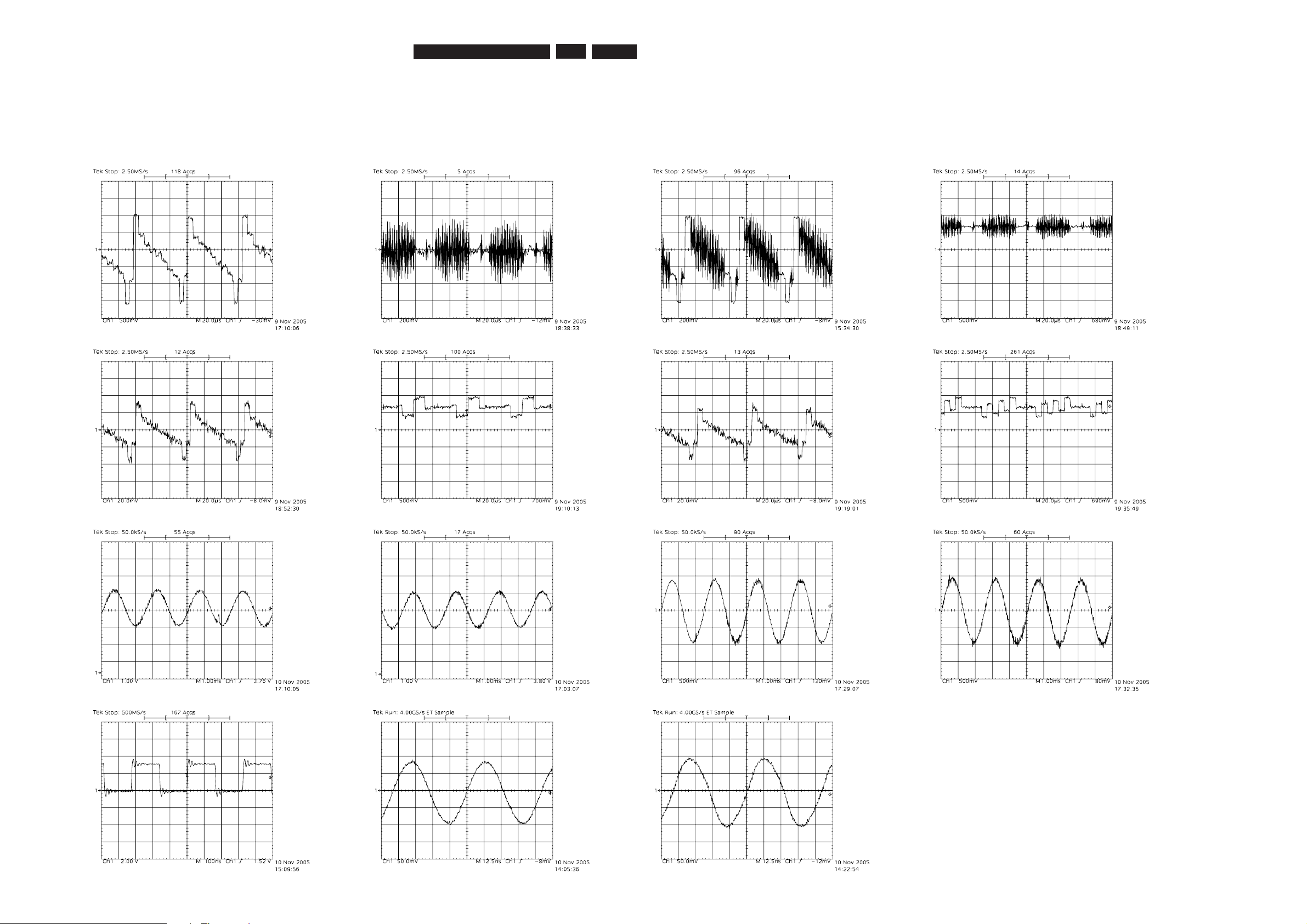
Waveforms
Waveforms of Analog Board
I143 Y_OUT I142 C_OUT I144 CVBS_OUT I137 D_C
I138 D_Y I139 D_VR I140 D_YG I141 D_UB
I213 AIA_R_RE1/AIA_R_RE2 I212/I214 I241 ALDAC (PIN 18 7206) I242 (PIN 15 7206)
I150 DIGITAL_OUT 7304MSP XTAL_IN 7304MSP XTAL_OUT
Page 18
EN 18
3139 785 3220x
6.
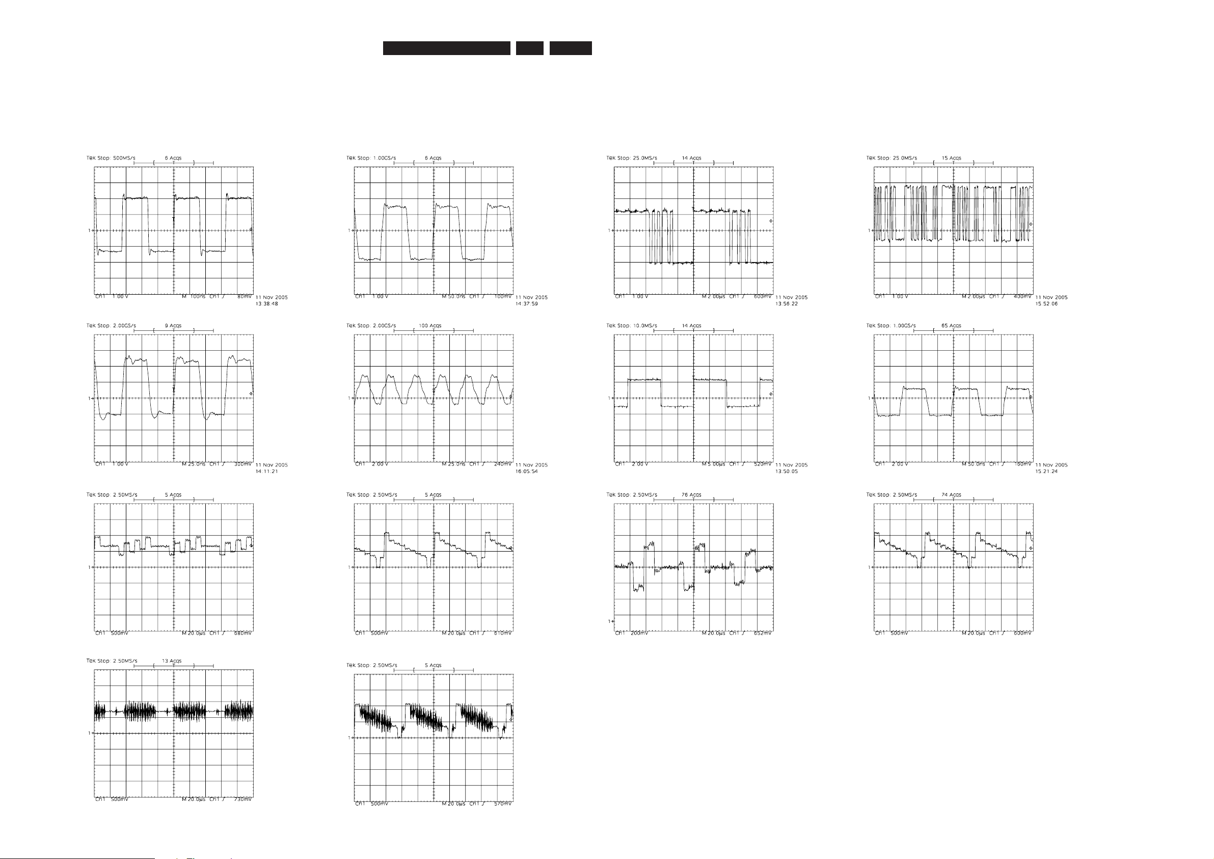
Block Diagrams, Waveforms, Wiring Diagram.
Waveforms of Digital Board
AUD_BCKI T537 AUD_BCKO T541 AUD_DAI(0) T539 AUD_DAO(0) T543
AUD_MCKI T540 AUD_MCKO T544 AUD_WCKI T538 AUD_WCKO T542
VOA_RPr T521VOA_BPb T518
VOA_CVBS T524
VOA_GY T520
VOA_SC T523
VOA_SY T522
Page 19
EN 19
3139 785 3220x
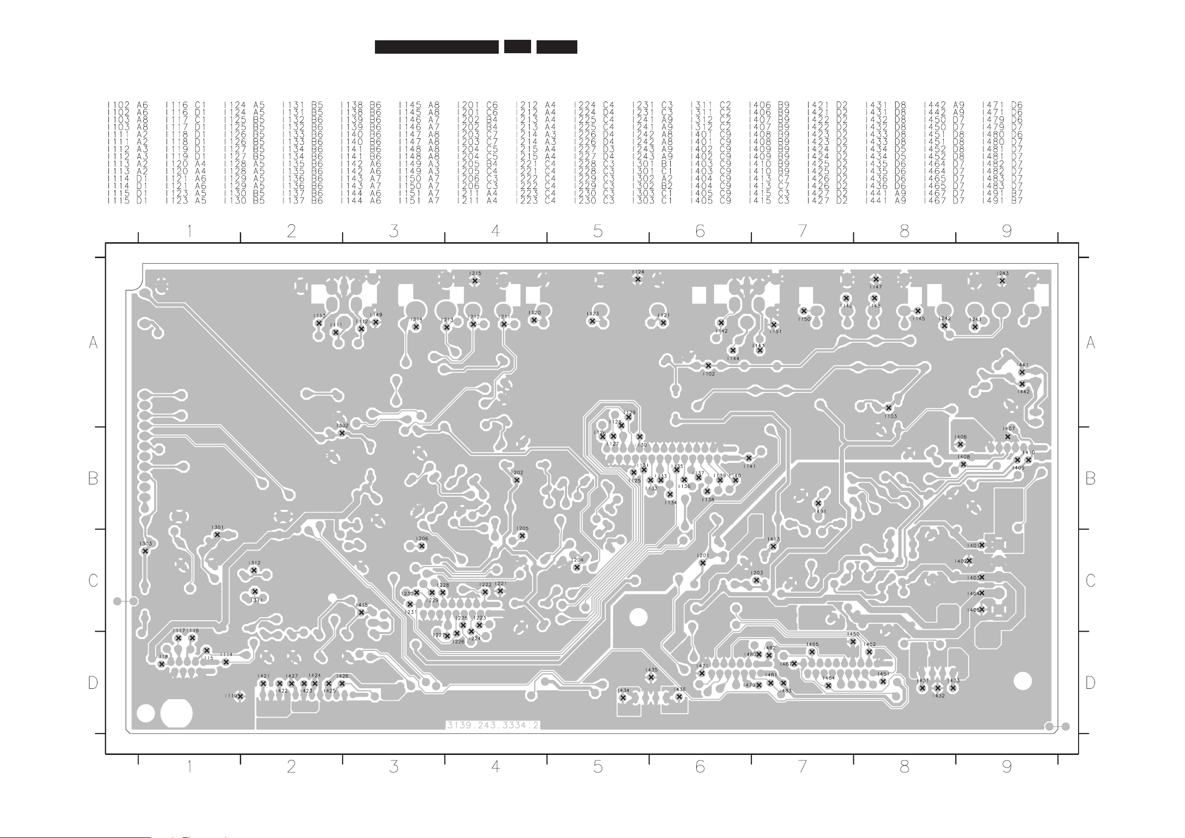
6.Block Diagrams, Waveforms, Wiring Diagram.
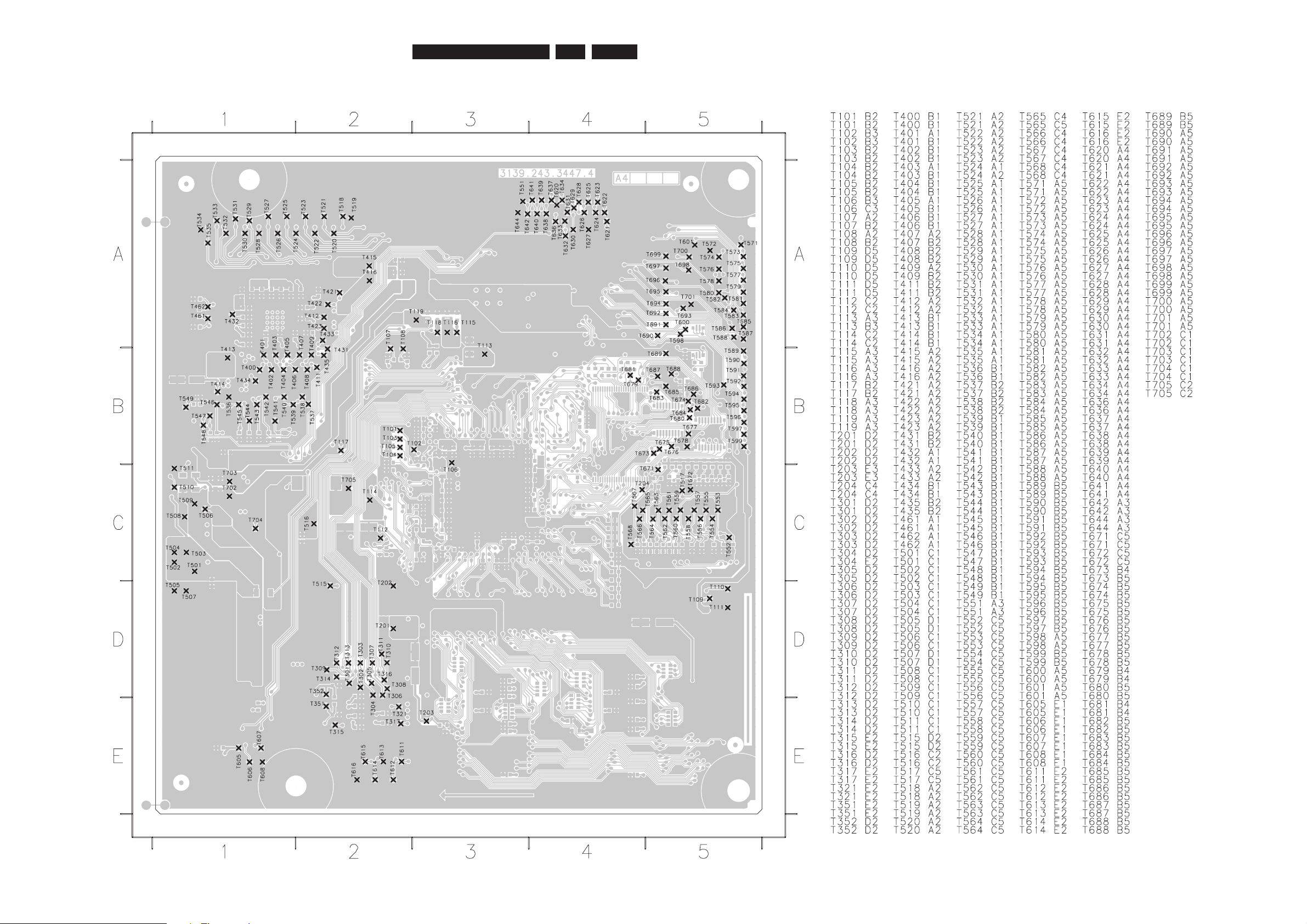
Test Points Overview for Analog Board
3380_APAC_TPOINT.pdf 2006-05-03
Page 20
EN 20
3139 785 3220x
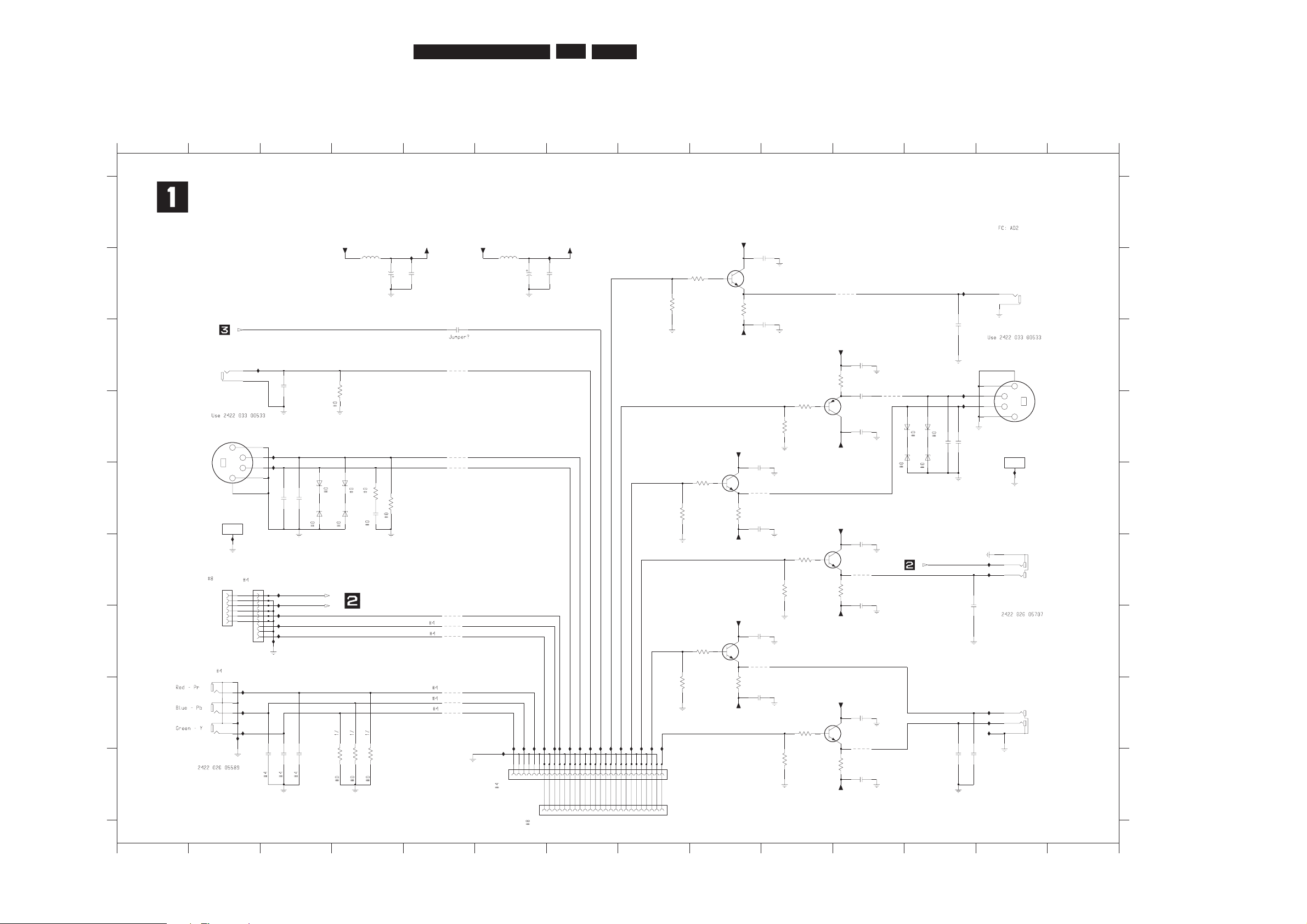
Test Points Overview for Digital Board
6.
Block Diagrams, Waveforms, Wiring Diagram.
DVDR3455D_TestPoint.pdf 2006-05-25
Page 21
EN 21
3139 785 3220x
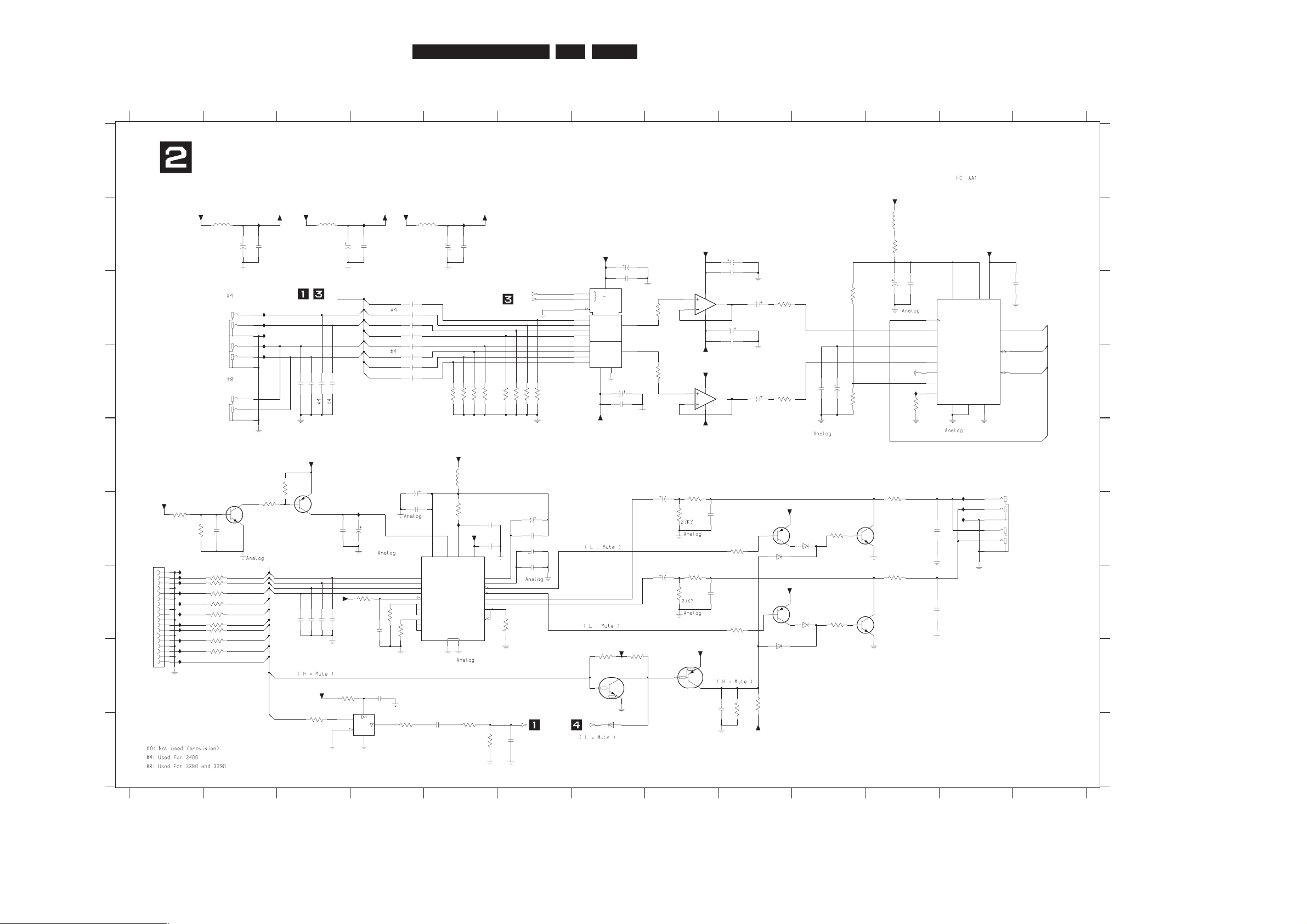
7. Circuit Diagrams and PWB Layouts
7.Circuit Diagrams and PWB Layouts
Analog: Video Input/Output
F
G
H
I
1111-A D2
1111-B C2
1111-C E2
1112 F2
1113 G2
1114 F2
1121 I6
2141 H9
2142 H11
2143 I11
2151 C12
2152 D12
2153 D12
2154 G12
2155 I12
2156 I12
3111 D4
3112 E4
1131-2 F13
Rear YC in
Pb out - Blue
1132-C D13
%1
1132-B B13
Front A/V in
1132-A C13
1122 I6
1131-1 H13
D
E
F
G
H
I
A
B
C
D
E
11
#8: Used for 3380 and 3390
91012345678
2139 F11
2140 G9
4113 G5
4114 G5
4115 E5
4116 G5
4117 H5
4118 H5
4119 H5
4121 B11
4122 D11
4123 E9
4124 F11
3114 I4
3115 I4
CVBS out
#0: Not used
%1
3113 E4
B
C
3122 B8
3123 B9
3124 C11
3125 D10
3126 D10
3127 E9
3128 E8
3129 E9
3130 F10
3131 F10
3132 F11
2137 E9
2136 E9
2138 F11
2134 D11
2133 C11
2135 D11
2132 C10
4111 C5
4112 D5
I141 H8
I142 D12
I143 D12
I144 B12
I145 H13
I146 F13
I147 H13
I148 H13
I149 F2
I150 F13
%1
3116 I4
3121 B9
I112 D3
I113 E3
I114 F3
I115 F3
I116 G3
I117 G3
I118 G3
I119 G3
I120 H2
I121 H2
I123 H2
6112 E4
5101 B4
6111 E3
Rear CVBS in
%1
5102 B6
4125 G9
4126 H11
I139 H8
I140 H8
Y
I124 H2
I125 H6
I126 H6
I127 H6
I128 H6
I129 H6
I130 H7
I131 H7
I132 H7
Pr out - Red
I103 B7
I111 C2
I151 E13
C
%1
I136 H7
I134 H7
%1
I138 H8
I135 H7
I133 H7
Y out - Green
C
6121 D12
6122 D12
6123 D11
6124 D12
7111 B9
7112 C10
7113 E9
7114 F10
7115 G9
7116 H10
I102 B5
3133 G9
%1
Tuner in
3135 H9
3134 H8
3138 I11
3137 H10
3136 I10
I137 H7
14
12345678910
#4: Used for 3400
6113 E3
6114 E4
11 12
from / to Digital Board
Video input / output
Digital out - Black
Y/C out
%1
Rear YUV in
Y
12 13
2101 B4
2102 B4
2103 B6
2104 B6
2111 C3
2112 E3
2113 E3
2114 E4
2115 I3
2116 I3
2117 I3
2121 C5
2131 B10
14
A
13
%1
GND
I115
2112
p001
2113
R57
GND
GND
R061
43
13
931I
5V
5V_V
5101
10u
5V_V
6313
R
06
1
100n
2131
2132
100n
2512
p001
150R
GND
GND
3121
150R
3137
R
03
3
2313
GND
7
6
5V_V
4123
3
4
5
1132-B
MSP-801V1-02-01-B NI FE LF
MSP-801V1-02-01-B NI FE LF
1132-A
1
2
p001
1112
4121
R
57
5
113
4119
2213
R061
2141
100n
GND
GNDGND
R033
9213
21C-483XZB
3216
3012
V61u01
I151
I150
5VN_V
I117
I112
I113
4124
R0
33
8313
p001
5
112
GND
150R
3127
5VN_V
p001
1512
141I
I143
0
4
1I
4111
GND
4113
4112
0u1
p001
31
1
2
4118
4117
GND
7116
BC847BW
5
4
6
GND
3
1
2
MSD-244V-88 NI FE LF
RED_BLACK
1131-2
MSD-244V-88 NI FE LF
GREEN_BLUE
1131-1
I146
4116
2
1
C-
48
3
XZB
1u02121
6
112
p001
5V_V
n001
4
0
1
2
5V_V
4216
21C-483XZB
I111
100n
2134
4114
GND
100n
2135
4122
I148
2012
n00
1
I114
10u
1012
5102
5VN_V
GND
V61
u01
3130
5V_V
5VN
3125
150R
150R
GND
R57
3
1
13
8213
R06
1
789
GND
GND
5
2
6
2
7
2
8
292
3
0
3
456
617181
9
1
2
0
2
1
2
22
3
2
42
1
2
11
7
C
2-S03
W
L
H
1
01
11
2
1
31
41
51
GND
21C-483XZB
3116
4112
I145
GND
p001
3512
p001
7112
6
7
8
9
I118
1
2
3
4
5
4115
1112
HLW9S-2C7
6
I103
1
2
3
4
5
8
1113
LPR6520-P910F
GND
MSP-801V1-02-01-B NI FE LF
1132-C
7114
BC847BW
72
1
I
211
6
2
1C-
48
3XZB
831I
R5
7
61
13
21C-483XZB
1116
5V_V
4
5
6
7
8
9
81
9
1
2
0
212
2
2
32
4
2
3
1
011
1
213
1
415
1
617
1
4213
R03
3
7
C
2
S4
2WLH
2211
GND
RES
BC847BW
7115
21C-483XZB
21C-483XZB
1216
4116
2216
GND
GND
GND
2133
100n
13
1
I
GND
4125
6512
100n
2140
p001
731
I
I142
531I
6
3
1I
I102
5512
p001
I144
GND
3133
150R
100n
2138
7111
BC847BW
6
1313
R
061
1
2
3
4
5
4512
p001
1114
HLW6S-2D7LF
I147
5VN_V
GND
GND
4126
GND
I124
031I
43
1I
BC857BW
7112
GND
3
3
1I
MSP-801V1-02-01-B NI FE LF
1
2
3
4
5
7
6
1111-A
GND
MSP-801V1-02-01-B NI FE LF
1111-B
2139
100n
R
57
4
1
13
GND
GND
GND
R57
11
13
GND
GND
GND
53
1
3
R0
3
3
I149
GND
GND
521I
23
1I
2142
100n
7113
BC847BW
I120
R033
321
3
I119
R061
62
1
3
I121
I123
921I
821I
2143
100n
2136
62
1
I
100n
1111-C
MSP-801V1-02-01-B NI FE LF
GND
8
5VN_V
2137
100n
VIA_GY
GND
5VN_V
5VN_V
I116
VO_SY
FR_CVBS_IN
AIA_L_FR
AIA_R_FR
RE_SY_IN
RE_SC_IN
VIA_SC_RE
VIA_SC_FR
VIA_RPr
VIA_BPb
DIGITAL_AUDIO
RE_CVBS_IN
RE_Y_IN
RE_Pb_IN
RE_Pr_IN
VO_Pb
VO_Y
V0_CVBS
VO_SC
VOA_GY
VOA_RPr
VOA_SY
VOA_SC
VOA_CVBS
VIA_CVBS_RE
VIA_SY_RE
VIA_CVBS_FR
VIA_SY_FR
FR_SC_IN
FR_SY_IN
VIA_CVBS_TU
VOA_BPb
TUN_CVBS
3139_243_33332_130_1_a2.pdf 2006-03-01
Page 22
EN 22
3139 785 3220x
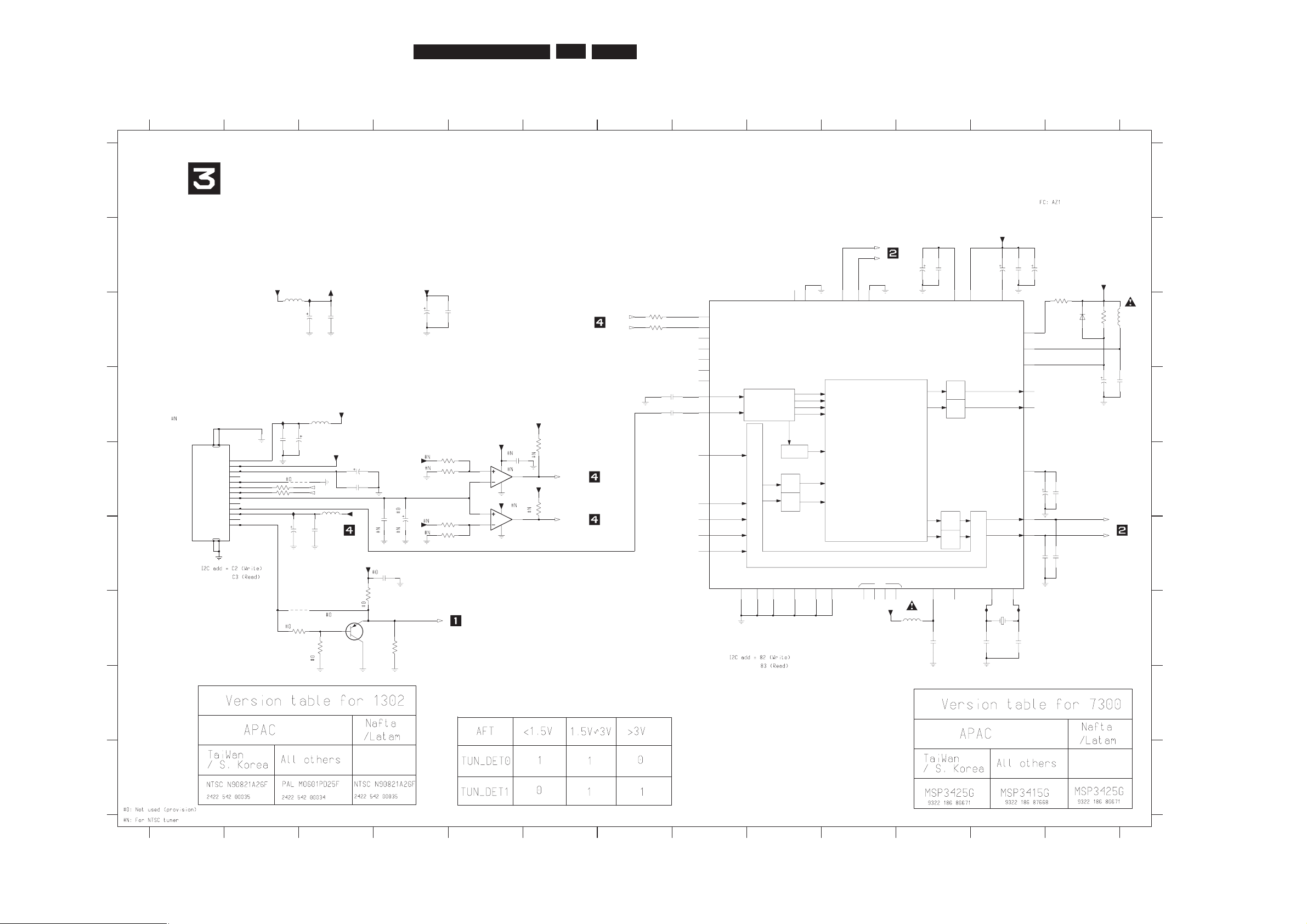
7.
Circuit Diagrams and PWB Layouts
Analog: Audio ADC/DAC
EN
DATAO
BCK
WS
VSSA VSSD
VDDD
VINR
SFOR
VINL
MSSEL
VREF
VRN
VDDA VRP
SYSCLK
PWON
SDA
CDIN
CCLK
SCL
AD0
CS
VQ
VBIAS
GND
SDIN
AMUTEC
BMUTEC
AOUTA
AOUTB
DEM
SCLK
LRCK
MCLK
RST
DIF0
DIF1
VLVDVA_HVA
G4
0
3
2
VDD
VEE VSS
1
0
3
2
1
4X
030
1
G
H
I
1201 D2
10 11 12 13
5678910111213
A
B
C
D
E
F
G
H
I
A
B
C
D
E
F
2210 D4
2211 D4
2212 D4
2231 B7
1202 C2
Audio-L out
123456789
2244 D10
2245 C11
2246 C11
2247 C12
1234
Audio input analog (AIA)
)DOIA( l
a
tig
i
d
t
up
t
uo
/
tu
p
ni o
i
d
uA
1203 F1
1205 E12
2201 D3
2202 D3
2203 D3
2204 D3
2205 C4
2206 C4
2207 C4
2208 C4
2209 C4
2265 G3
2266 G4
2271 F8
2272 F8
2232 C7
2233 D7
2234 D7
2235 B9
Rear audio in 1
Audio-R out
2236 B9
2237 C9
2238 C9
2241 C9
2242 D9
2243 D10
2295 B5
2296 B5
3201 D5
3202 D5
2251 F2
2252 F3
2253 F4
2254 E4
2255 F4
2256 F5
2257 F5
2258 F6
2259 F6
2260 F6
2261 G6
2262 G3
2263 G3
2264 G3
3216 D10
3217 D11
3221 F1
3222 F1
2273 G8
2274 G8
2275 F11
2276 G11
)DOIA( latigid tuptuo / tupni oiduA
2281 H4
2282 I5
2283 I6
2284 I8
2291 B2
2292 B2
2293 B3
2294 B4
3237 G2
3238 G2
3239 H2
3241 F8
3203 D5
3204 D5
3205 D6
3206 D6
2422 026 05383
3207 D6
3208 D6
3211 C8
3212 D8
3213 C9
3214 D9
3215 C10
3260 I3
3261 H3
3262 I4
3263 I5
3223 F2
3224 E3
3225 G4
3226 G4
3227 G4
3228 G6
3229 F5
3231 G2
3232 G2
3233 G2
3234 G2
3235 G2
3236 G2
6204 F10
6205 G10
7201 C7
7202-1 D8
3242 F8
3243 G8
3244 G8
3245 F9
3246 F10
3247 G9
3248 G10
3249 F11
3250 G11
3251 H7
3252 H7
3253 I9
3254 I9
I206 D11
I211 C2
I212 C2
I213 C2
3264 I5
3265 B11
5201 B2
5202 B3
5203 B5
5211 B11
5212 E5
6201 I7
6202 F9
6203 H9
I242 F12
I243 F12
7202-2 C8
7203 C12
7204 F2
7205 F3
2422 026 05462
Rear audio in 2
d
ra
oB
la
tig
i
D ot
/mo
r
f
7206 G5
7207 F9
7208 F10
7209 G9
7210 G10
7211 H7
7212 H8
7214 H4
I201 B2
I202 B4
I203 B5
I204 F4
I205 F5
I214 D2
I215 C2
I221 G1
I222 G1
Audio ADC / DAC
I223 G1
I224 G1
I225 G1
I226 G1
I227 G1
I228 G1
I229 G1
I230 H1
I231 H1
I241 F12
2K2
3245
22R
5V_A
6.3V
3233
2254
100u
4
5
p0016722
3
1
2
6
LPR6520-J440G
1205
I229
K0014023
100R
3250
2722
0n1
2
3
4
5
6
7
8
9
10
11
12
13
14
15
16
17
18
1203
HLW18S-2C7
1
K001
10
2
3
GND
p333622
3
1
2
GND
LPR6520-J920G
1201
4922
n001
3V3_A
I241
GND
I231
I221
2233
47u 6.3V
100n
2234
BAS316
1u0
2209
6202
2271
DN
G
5V_A
22u16V
p001
4022
3V3_A
3V3_A
I206
u001
1125
I205
2
3
1
5
4
7214
74LVC1G125GW
5V
12V
K0012023
p
33262
2
6.3V
2242
47u
n001
6422
3243
680R
1u0
2208
3235
2212 1u0
22R
100K3225
100n2256
GND
1123
0K1
22n
2259
5VN_A
5VN
1
3
2
1K0
3223
3422
7210
BC817-25W
n001
22R3237
3V3_A
3249
I230
100R
5VN_A
I228
GND
2235
47u 6.3V
13
22R
3231
4
10
2
1
117
1
12
5
0
2
7206
19
18
15
14
9
8
7
6
61
3
CS4351
192 kHz DAC
Φ
100n
2236
0K1
7123
9
1
3
2
4
5
51
01
12
UDA1361TS
ADC
Φ
24-BIT AUDIO
7203
11
13
14
7
6
8
61
GND
I227
GND
I226
p
334622
n0
01
29
2
2
BC857BW
7207
GND
7205
1
3
2
V3.6u74
4
422
BC807-25W
5VN_A
K0013023
16V 47u2260
GND
GND
3V3
V61u
7
4
3522
GND
GND
K51
44
2
3
3232
GND
I204
10K
22R
3214
5V_A
K01
8
2
23
0
n1
4722
50
2
3
K
0
01
K
0
01
8
0
23
5V_A
3241
680R
2281 100n
3239 22R
6201
BAS316
3260
4
I243
1K0
LM833
7202-1
NULL
3
2
1
8
GND
GND
K0016023
470R
3261
1u0
3V3_A
GND
2207
2232
100n
p001
5722
47u
2258
16V
p0012022
I214
GND
GND
GND
K51
7422
n001
24
2
3
3
2
K0
0
1452
3
PDTC124EU
7211
1
p
335622
5V
5VSTBY
4K7
3251
I224
5
15
2
11
4
13
3
10
9
6
61
7
8
12
1
14
7201
HEF4052B
MDX
10u
5202
3V3_A
10K
3213
BC847BW
1
3
2
GND
GND
7204
GND
2205
1u0
6203
BAS316
GND
100n
2238
9K3
2K2
3247
4223
n0
0
1
1522
I242
1u02211
100n
2255
2257
1K0
3246
100n
I223
I222
I213
2206
1u0
p
001102
2
100n2261
K74
612
3
1u0
2210
5VN_A
GND
GND
0K1
2
12
3
3238
GND
5VN_A
22R
2282 8n2
4822
n
22
BC817-25W
1
3
2
7212
1
3
2
GND
7208
7u4
PDTA124EU
6
622
I211
I212
2237
47u 6.3V
I215
K74
5123
7023
1922
V61u01
K001
5201
10u
3523
K22
2273
3262
16V 22u
75R
n001
2522
3248
1K0
3V3_A
I225
R22
5
623
I202
5VSTBY
5V_A
GND
I201
6205
BAS316
6204
BAS316
R
0
514623
GND
7209
BC857BW
V3.60m1
5422
22K
3252
K
0122
2
3
GND
GND
47u
2241
7
8
4
6.3V
LM833
NULL
7202-2
5
6
3263
GND
120R
K01
7
22
3
V61u01
3922
22R
3234
2125
u22
p093
GND
GND
3
8
22
I203
9
223
7R4
5VSTBY
6.3V47u
2231
3236 22R
6223
K0
1
GND
V61
n001
6922
5922
u01
6
4
5
5203
10u
1202
LPR6520-J440G
3
1
2
GND
GND
4K7
3221
GND
3022
p001
AOD_WCK
AOD_MCK
AID_WCK
AID_BCK
AID_MCK
AID_DAT
AID_DAT
AIA_R_RE2
AIA_L_RE2
AIA_R_RE1
AIA_L_FR
AIO_MUTE
DIGITAL_AUDIO
AIA_L_RE1
AOD_SPDIF
AIA_R_FR
AIA_L_MSP
AIA_R_MSP
AIA_R_RE1
AIA_L_RE1
AIA_L_RE2
AIA_R_RE2
AOD_SPDIF
AMUTEC
BMUTEC
AOD_BCK
AOD_WCK
AOD_MCK
AOD_DAT
AID_BCK
AID_WCK
AID_MCK
AOD_BCK
AIO_MUTE
AOD_DAT
AKILL
RSA2
RSA1
POWER_FAIL
3139_243_33332_130_2_a2.pdf 2006-03-01
Page 23
EN 23
3139 785 3220x
7.Circuit Diagrams and PWB Layouts
Analog: Tuner and Multi-Sound Processor (MSP)
LOUDSPEAKER L
D/A
D/A
I2SL/R
HEADPHONE R
IDENT
NC
SCART
LOUDSPEAKER R
A/D
D/A
DEMODULATOR
S1...4
FM1
FM2
I2SL/R
NICAM B
NICAM A
SCART-L
HEADPHONE L
IDENT
LOUDSPEAKER
A/D
D/A
SCART-L
SCART-R
DFP
SCART-R
Switching Facilities
TMTMTM
TM
5311 D3
5312 E3
5321 C13
5322 G11
6311 C13
3313 G3
3314 G2
3315 G3
3316 G4
3326 E6
4311 E2
4312 G2
5301 C2
2321 B11
2322 B11
2323 B12
2324 B12
2325 B12
2326 D13
2327 D13
2328 E12
2329 E13
7302 G3
7303-1 E5
7303-2 E5
7304 C8
I301 D2
I301 C3
I303 E3
I311 G12
I312 G12
2302 C3
3317 E4
3318 E4
3319 F4
3320 F4
3321 E6
3322 C7
3323 C7
3324 C13
3325 C13
2317 F4
2318 E5
2319 F4
C
2330 F12
2331 F13
2332 G11
2333 G12
2334 G12
2335 D7
2336 D7
3311 E2
3312 E2
2303 C4
2304 C4
2310 E2
2311 E2
2312 E3
2313 E3
2314 F2
2315 F3
2316 F4
D
E
F
G
H
I
A
B
C
11 12 13
A
B
3456
78910
78910
D
11 12 13
12
1301 G12
1302 D1
1303 D1
2301 C3
E
F
G
H
I
123456
Tuner and multi sound processor (MSP)
LM393D
5
67
84
7303-2
3312
100R
2319
100n
V61
u01
3232
K
0
1
6233
SCL
7
SDA
SIF_OUT
10
13
VIDEO_OUT
11
VT
I301
AUDIO_OUT
2
B+
41
6
1
5
1
71
3
NC
4
NC
NC
12
6
RENUT
TCSN9082PA26F(H)
1303
8
AFT_OUT
AS
5
9
1232
u01V61
4312
I303
I302
5V_FV
POTFERV
24
NI_LATX
5
TUO_LATX
6
I312
30
SC2_IN_L37
SC2_IN_R38
STBYQ
11
N
E
TS
ET
4
PT
7
1FE
R
V
92
2FE
R
V
5
2
32
42
82
23
RESETQ
22
SC1_IN_L40
SC1_IN_R41
SC1_OUT_L 31
SC1_OUT_R
I2C_CL
12
I2C_DA
13
I2S_CL
14
I2S_DA_IN1
17
I2S_DA_IN2
21
I2S_DA_OUT
16
I2S_WS
15
MONO_IN43
1
M_LPAC
43
DACM_L 27
DACM_R 26
S
SVD
0
2
DVSUP
19
0OI_RTC_D
9
1OI_RTC_D
8
AGNDC
36
SSVHA
53
PUSVHA
33
ANA_IN+2
ANA_IN-3
GSA
93
S
S
V
A
44
PUSVA
MSP3425G
7304
LC_RDA
81
LES_RDA
0
1
5301
47u
56p2335
18M432
1301
3320
n001
10K
I311
2332
3323
100R
413
2
V
0
5
7u
4
5322
5V
10u
33VSTBY
V01
1032
u022
313
3
2K2
5V_FV
8p64332
5V_FV
2032
n001
4K7
3317
5V_FV
8p63332
4311
5V_FV
V05
7132
2u2
2312
10u 16V
n001
4232
51
3
2
n
01
100R
3322
5232
V61u74
5133
22u
R001
5V
5312
1233
K
0
1
3
12
NC
SCL
6
7
SDA
SIF_OUT
10
VIDEO_OUT
13
VT
11
AFT_OUT
AS
5
AUDIO_OUT
9
2
B+
1
BB+
41
615
1
71
NC
1302
TCSM0601PD25F(H)
RENUT
8
3
21
84
7303-1
LM393D
n0
33
5V
VF_V5
61
3
2
u01
1235
n001
4
0
32
0n11332
1136
613SAB
5V
5V_FV
7302
BC857BW
6u85311
8V
n001
9232
100n
5V
VF_V5
2313
n0011132
0n10332
6232
u01
V61
3325 10K
R57
6133
3318
10K
3319
2336 1u0
27K
100R
3311
7232
n001
V
61u0
1
0132
2232
n001
7K4
4233
u0
1
30
3
2
5V_FV
V61
3314
100R
8232
V057u4
100n
2318
TUN_DET0
TUN_DET1
TUN_CVBS
RSA2
RSA1
AIA_L_MSP
AIA_R_MSP
SCL_5V
SDA_5V
SCL_5V
SDA_5V
3139_243_33332_130_3_a2.pdf 2006-03-01
Page 24
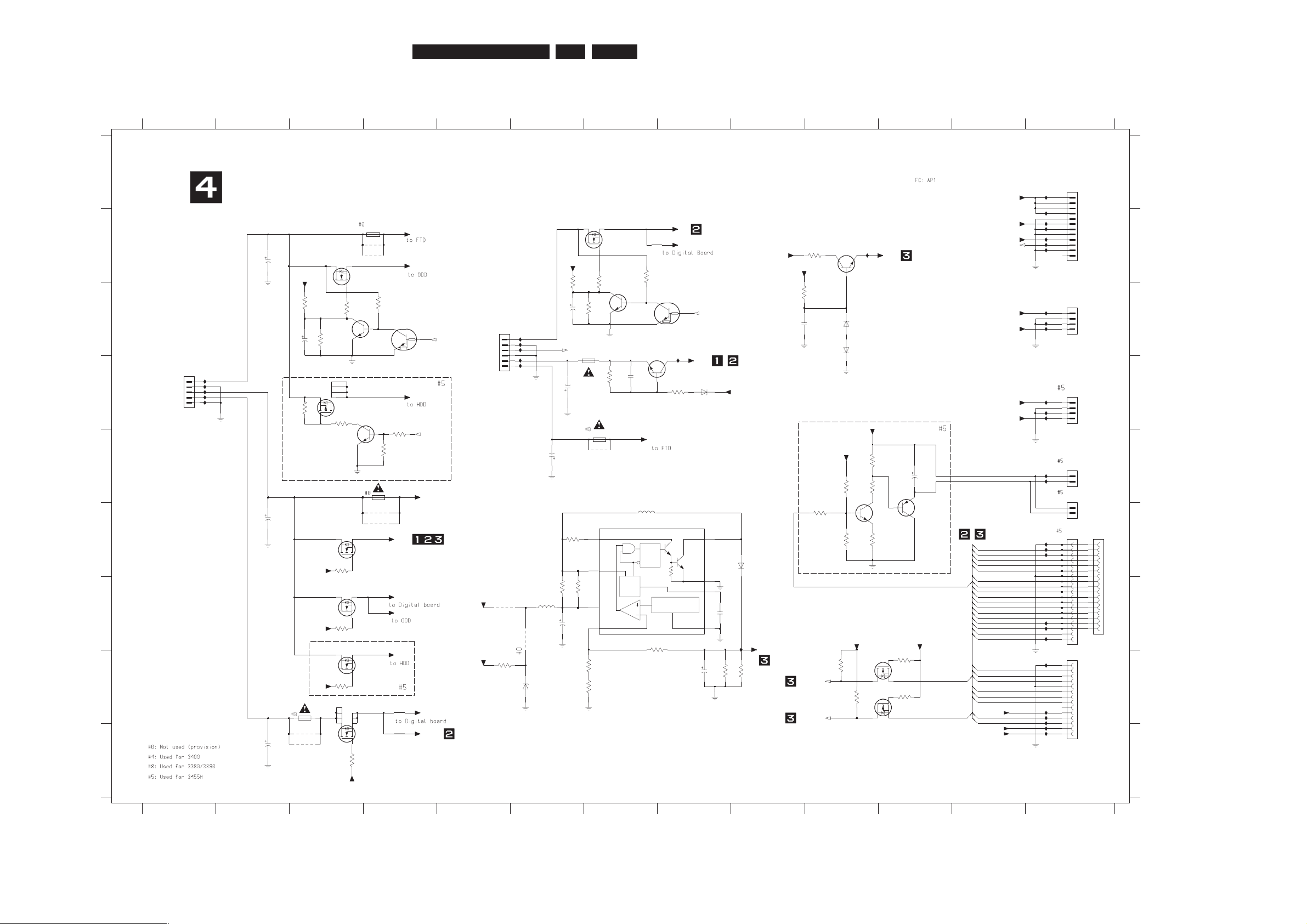
EN 24
3139 785 3220x
7.
Circuit Diagrams and PWB Layouts
Analog: PSU and Interfaces
1408 F13
1409 H13
1413 H3
1414 C6
1415 E7
1234
3427 B10
B
C
567
G
H
I
draob latigid ot noitacinummoC
4415 F4
2419 C6
2421 G6
1410 E13
1411 B3
1412 E4
3410 C3
3411 C3
3412 C3
L = Standby
3413 C4
3414 D3
3415 D3
3416 D4
3417 E4
3418 F3
3419 H3
3420 I3
3421 B6
3422 C7
3423 C7
3424 B7
3425 D7
3426 D8
7420 C7
3428 C9
3429 G3
D
E
F
3434 H7
3435 H7
3436 H8
3437 G7
3438 H9
3439 H5
3441 F10
3442 E10
3443 F10
3444 E10
3445 E10
3446 F10
3451 H10
3452 H10
3453 H11
3454 H11
4411 G5
4412 G6
4413 B4
4414 B4
4416 F4
4417 I3
2422 H8
2423 G8
2431 E11
5412 F7
6411 D8
6412 C10
H = On
6413 C10
6421 F9
6422 H6
7411 B3
7412 C4
7413 C3
7414 D3
7415 D4
7416 F3
7417 G3
7418 I3
7419 B7
I435 D13
7421 C8
7422 C7
3431 F6
3432 G6
3433 G6
7426 G3
7431 F7
7441 H10
DDO ot
draob tnorf ot noitacinummoC
PSU and interfaces
1405 D13
7442 H10
I401 D1
4418 I3
4419 E7
5411 G6
I405 D1
I406 C6
I407 C6
draoB latigiD ot
I408 C6
I409 D6
I410 D6
I413 D8
I415 B10
I421 A13
I422 B13
I423 B13
I424 B13
I425 B13
I426 B13
I427 B13
I431 C13
I432 C13
I433 C13
I434 D13
7423 B10
7424 F11
7425 E11
2413 F2
2414 I2
2415 D6
2416 D7
2417 C9
DDH ot
1406 E13
1407 F13
I
1401 D1
1402 C5
1403 A13
1404 C13
I450 F13
I451 F13
I452 F13
I402 D1
I403 D1
I404 D1
I471 H13
I479 H13
I480 H13
I481 H13
I482 I13
I483 I13
A
B
C
D
E
F
G
H
2418 E6
NAF ot
2411 B2
2412 C3
I491 G9
Fr MCU
I436 D13
I441 E13
I442 E13
12
I464 G13
I465 G13
I467 G13
13
A
11
8 9 10 11 12 13
12
7
142
345678910
n001
I467
5VH
8V
I479
344
3
7K4
I450
12VBE
I402
91
4
2
V050u1
5VE
4416
4418
4415
4414
4417
4413
2144
GND
12VSTBY
4419
3418
10K
BC847BW
12V
7420
1
2
BC327-25
7425
2
B2B-EH-A
1410
1406
B2B-EH-A
1
12
4
6
6
13SAB
1
2
43
K001
3K
3
4443
I431
534
3
R0
01
3439
1K0
GND
5VH
DNG
5243
K74
GND
SI2306DS
7416
12V
12V
K74
3143
7K4
2443
1
2
3
4
I410
B4B-EH-A
1405
GND
u033
1142
3
1
46
6
1
3
SAB
3454
1K0
I423
3V3
GND
V2
1
6411
BZX384-C6V8
10K
3429
BC847BW
7424
GND
GND
1K0
3453
V05u01
8142
I405
T125mA
1414
2246
2
V8
C
-48
3
XZB
3431
100R
6
3
4
I426
7414
SI3443DV
1
2
5
0
R1
5443
2V8C-
4
83X
Z
B
2146
I432
GND
I422
33VSTBY
I424
8K
1
43
4
3
K022
GND
12VH
2243
7415
BC847BW
4411
I451
I434
u
0
01
I435
514
2
19
2
3
4
5
6
7
8
9
1
10
11
12
13
14
15
16
17
18
HLW19S-2C7
1407
I442
5VSTBY
BSH103
7442
I425
I406
I483
1
2
3
4
5
6
PDTC124EU
7421
1402
B6B-PH-K
V05u001
224
2
12VE
I464
I421
8
9
I471
1
10
11
12
2
3
4
5
6
7
B12P-PH-K
1403
5V
I413
STS9NF30L
12VSTBY
5V
7418
0243
7417
SI2306DS
6142
n
001
K
81
SI2306DS
7411
I403
3441
68R
8243
7K4
5VN
1543
7K4
7K4
25
43
u065
4
1
4
2
1000mAT
33VSTBY
4
5
1412
B5P-VH
1401
1
2
3
I465
2A T1413
I491
GND
I427
3242
p
093
3V3BE
V21
3V3BE
I480
I407
GND
V0
1
u0
0
1
1242
3K3
I436
2143
10K
3419
12VH
12VE
K022
0143
GND
12V
3243
3
K3
5VBE
12VBE
5VBE
0
K1
BSH103
64
43
GND
7441
5
R
1
2
3
43
K7
4
4243
VGNSTBY
4143
K74
K
22
83
43
3V3
I452
u
065
3142
GND
6
343
K
22
GND
12
13
14
2
3
4
5
6
7
8
9
1
10
11
I415
HLW14S-2C7
1409
7143
33VSTBY
12V
K74
I433
500mA
T
1411
125mA T1415
3K3
3415
3416
3K3
5
6
7
8
9
I441
12
13
14
15
16
17
2
3
4
1408
HLW17S-2C7
1
10
11
K001
11
4
3
33
43
5R
1
1K5
3426
5412
BC337-25
7422
1m0
BC847BW
7413
HV21
12V
I481
I482
V52u01
1342
100R
3427
PDTC124EU
7412
1404
B4B-EH-A
1
2
3
4
I409
I408
5VSTBY
5VE
7423
BC547B
I401
2142
V05
2
u2
7419
SI2306DS
5V
I404
3437
47K
IS7
SWC 1
SWE 2
TIMC 3
VCC
6
7426
SI2306DS
7431
MC34063AD
REGULATOR
REFERENCE
OSC
IPK
QRS
CIN_NEG5
DCOL8
GND 4
33u
5411
AIN_SEL1
5V_VH
12V_P
TUN_DET1
POWER_FAIL
VGN_P
FBS
5VN_P
5VSTBY
3V3_VH
12V_VH
HDMI_INT
8SC2_1
TUN_DET0
DFM
SDA_3V3
8SC2_2
AIN_SEL0
ATNFM
POWER_FAIL
HDD_ON
SCKFM
DFM
DHOST
RDYFM
ATNFM
HOSTRST#
SCL_5V
SDA_5V
SDA_3V3
SCL_3V3
FAN
HOSTRST#
SCKFM
DHOST
RDYFM
SCL_3V3
HDD_ON
FAN
STBYn
VGNSTBY
12VSTBY
STBYn
STBYn
3139_243_33332_130_4_a2.pdf 2006-03-01
Page 25
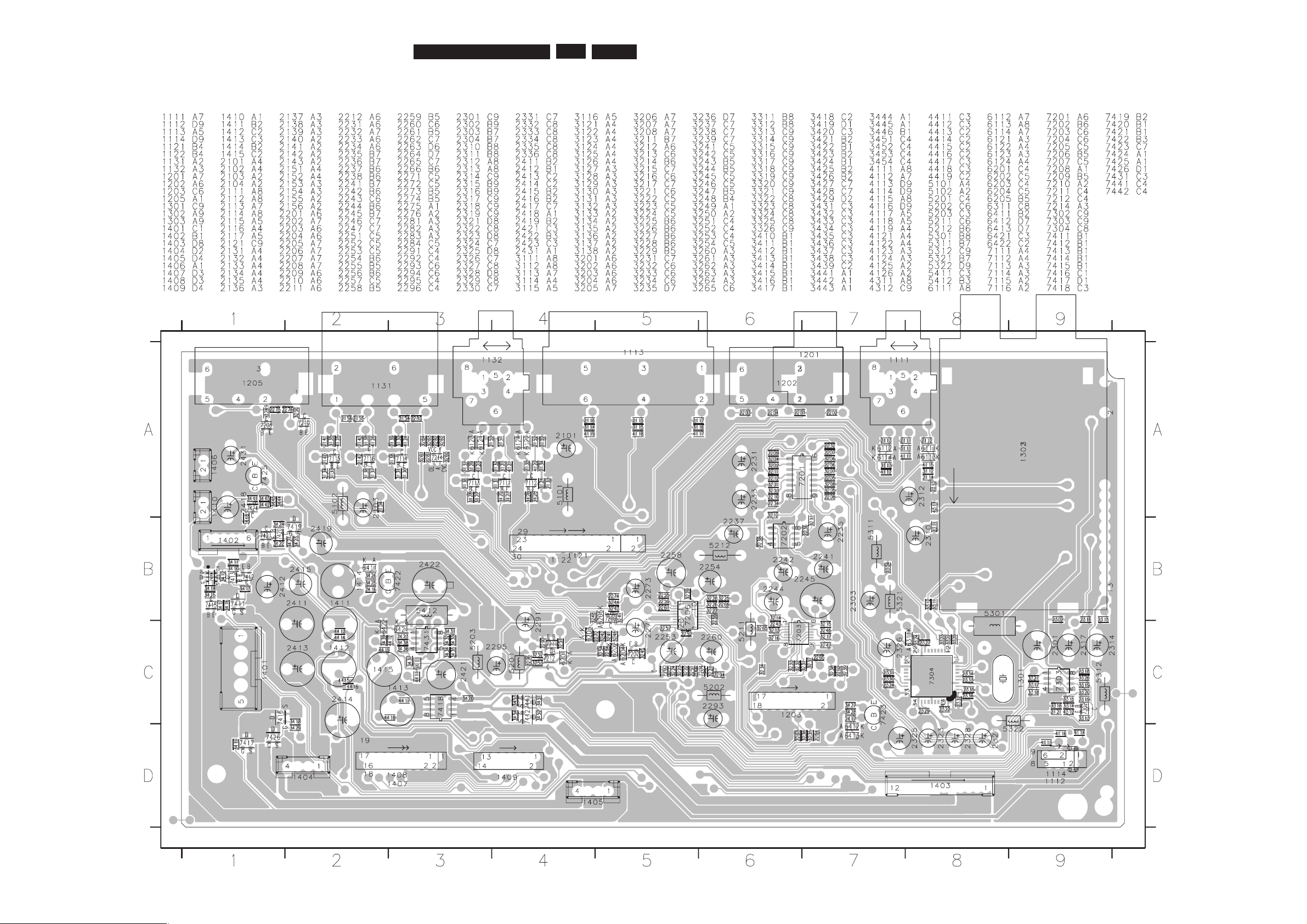
EN 25
3139 785 3220x
7.Circuit Diagrams and PWB Layouts
Layout: Analog-Main Part (Top View)
3380_APAC_TOPLAYR.pdf 2006-05-25
Page 26
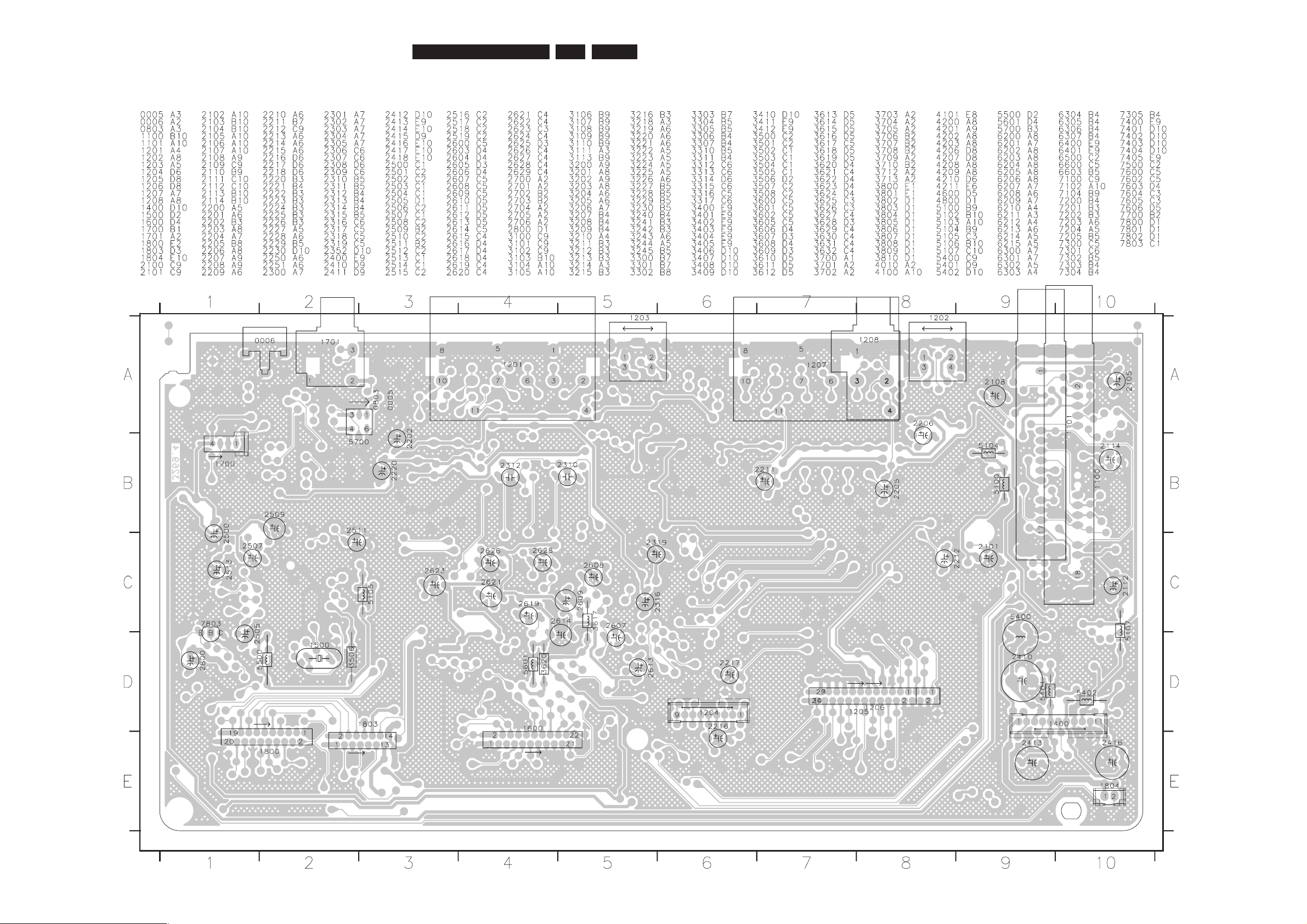
EN 26
3139 785 3220x
7.
Circuit Diagrams and PWB Layouts
Layout: Analog-Main Part (Bottom View)
TopView_AnalogBd_Hmc_32694.pdf 2005-05-25
Page 27
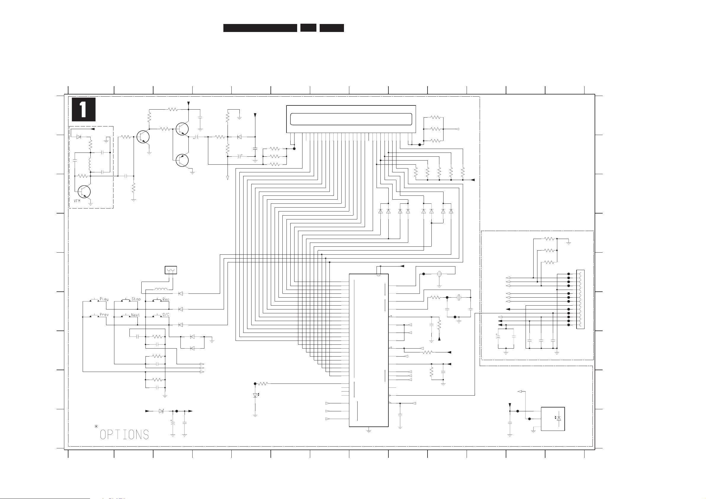
EN 27
3139 785 3220x
7.Circuit Diagrams and PWB Layouts
Front: Front Panel - Display
FIP
LED
Φ
FIP
CTRL
DRIVER
X
XT
KEY_R
FM
SCK
D
D_HOST
SCK1
POWER_FAIL
IR
VLOAD
1
2
3
IC
1
2
3
4 POWER_CTL
VDD
VSS
24
1
2
3
4
5
6
7
8
9
10
11
12
13
14
15
16
17
18
19
20
21
22
23
0
RDY
RESET
2
1
2
ATN
HOST_RESET
1
F113 F13
F114 F13
F115 E9
F117 F10
6117 H5
7100 A3
7101 B2
7102 B3
7103 C1
7105 H13
F100 B6
F101 B9
F102 E13
F103 E13
F104 E13
F105 E13
F106 F13
F107 F13
F108 F13
F110 F13
F111 F13
F112 F13
6104 D9
6105 D9
6106 D9
DC0
6107 D10
6108 D10
6109 D10
6111 E3
6112 F3
6113 F3
6114 G3
6115 G3
6116 H3
3116 D13
3117 D13
3118 E13
WS0
3119 F10
3120 F10
3121 G2
3122 G9
3123 G2
3124 H10
3125 H2
3126 H6
3127 B9
3128 B9
3129 B10
3130 B10
3131 B10
5100 B1
5101 E3
6100 B1
6101 A5
6102 D8
6103 D9
3100 A3
3101 A2
3102 A4
3103 A10
3104 A3
3105 A10
3106 A2
3107 A4
3108 B10
3109 B1
3110 B4
3111 B5
3112 B6
3113 B6
3114 B1
3115 C2
C
D
E
2103 B1
2104 B5
2105 B1
2106 B1
2107 B2
2108 F10
2109 F11
2110 F9
2111 G2
2112 G11
2113 G12
2114 G12
2115 G12
2116 G13
2117 G2
2118 G2
2119 H10
2120 H3
2121 I9
2122 I3
2123 I3
2124 I12
10 11 12 13
A
B
C
D
E
F
G
H
I
A
B
2100 A4
2101 B4
2102 B5
1 2 3 4 5 6 7 8 9 10111213
1 23456789
F121 H3
F122 H12
F123 I12
F
G
H
I
0010 E3
1100 A6
1101 F1
1102 F2
1103 F2
1104 F1
1105 F2
1106 F2
1107 E10
1108 F10
1109 F13
2101
22u
F119 F10
F120 H5
F122
50V
F123
F120
F119
F121
F105
1108
F117
F111
32K768
F113
F108
F106
F107
F110
51
1
3
0K1
4016
613SAB
613SAB3016
0u1
2110
5101
K
28
0313
K28
9
21
3
821
3
K28
K
28
7213
3105
GND
10R
3104
470R
3112
F102
10R
2120
2n2
330R
10K3125
3126
n001
EVQ11L05R
5012
n001
4
2
12
1106
2212
2106
V
3
.6
0m
1
220n
2K7
3117
3116
2K7
311
2
GND
GND
n0
01
BAS316
6100
10
13
R033
GND
2012
n7
4
EVQ11L05R
1102
WH02D-1
0010
12
EVQ11L05R
1101
6K8
3114
2117
2n2
n0
01
61
12
n001
5112
F115
BAS316
6112
47K
1
27
28
52
51
50
2
3
3122
46
47
48 44
12
5
4
8
11
20
21
22
23
7
49
13
41
42
43
45
35
16
36
37
38
39
40
17
18
19
15
24
25
26
29
30
31
32
33
34
6
9
10
14
n
01
9
112
3100
330R
BC847BW
7103
3
P
814P715P616P517P418P31
9
P
21
01
11
P
9
21P
8
31P
7
41P
6
5
1P
5
61P
4
71P
2P
9122
11F
1
2
21F
12F
13
23
22F
C
N
121P02
01P
11
G1
92
82
G
2
G3
72
G
4
62
52
G5
4
2
G6
G732G8
31
1100
HUV-08SS65T
1107
2
35V22u
2104
6
13S
A
B9
0
16
613SAB7016
613SA
B
8016
613SAB
6016
GND
GND
10K
3121
2118
2n2
3123 10K
9
012
p22
8012
p22
1n0
2107
GND
6114
BZX384-C6V8
K01
2013
0012
n74
BAS316
6113
613SAB50
16
1
21
2
n00
1
NNTEK618LTL
7116
0K1
0113
R074
3109
6115
BAS316
BAS316
6111
3103
10R
2
0
16
61
3
SAB
3108
GND
GND
10R
F104
GND
F103
BC847BW
7101
3106
33R
F100
GND
GND
OUT
VS
7105
TSOP4836ZC1
GND
5100
u001
7102
EVQ11L05R
2SB1132
2
3
4
5
6
7
8
9
1103
1
10
11
12
13
14
F101
HLW14S-2C7
1109
2103
220n
EVQ11L05R
1104
7100
GND
2SD1664
GND
BAT54 COL
6116
n001
4112
3113
10R
2K7
3118
3212
GND
n01
K07
2
4
213
GND
3119
100R
V6
1
u001
211
2
BZX384-C6V8
6101
470R
3107
K74021
3
2n2
2111
K
28
1313
F114
1105
EVQ11L05R
GND
F112
RC
HOST_RESET
VGNSTBY
10R
3111
POWER_CTL
RDY_FM
ATN_FM5VSTBY
D_FM
12VSTBY
5VSTBY
KEY_B
5VLP
GND
POWER_FAIL
VGNSTBY
D_HOST
5VLP
SCK
5VSTBY
POWER_FAIL
RC
VGNSTBY
KEY_A
KEY_B
KEY_C
KEY_C
KEY_A
5VLP
SCK
D_FM
D_HOST
RDY_FM
ATN_FM
HOST_RESET
5VSTBY
12VSTBY
5VSTBY F2
VGNSTBY
2
F
3139_243_33314_130_1_a3.pdf 2006-02-28
Page 28
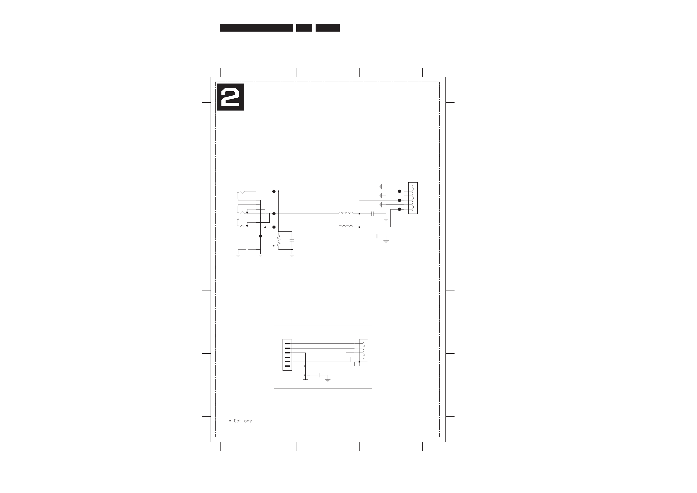
EN 28
3139 785 3220x
7.
Circuit Diagrams and PWB Layouts
Front: Front Panel - Audio/Video-In
2214 E2
2215 C1
3211 B2
3212 B2
3213 C1
F203 B1
F204 B1
F205 B1
F206 C1
F209 B3
F211 B3
F212 B3
I LINK 1394
123
123
A
B
C
D
E
A
IO0
B
C
D
E
1200 D3
1201 D1
1202 B3
1203-1 B1
1203-2 B1
1203-3 C1
2211 B3
2212 C3
2213 C1
5
6
AV_GND
HLW6R-2C7
1202
1
2
3
4
6
1
2
3
4
5
5
6
AV_GND
1200
CSS5004-7A01E
1201
S6B-PH-K
1
2
3
4
F212
AV_GND
3211
AV_GND
600R
R57
3123
1u0
GND
2211
2214
AV_GND
470p
F209
AV_GND
F203
GND
470p
2212
1u0
2215
F205
3122
p001
1203-3
RED
8
6
7
AV_GND
1203-2
WHITE
5
3
4
F204
F211
600R
3212
F206
AV_GND
1203-1
YELLOW
LPV8529-0100F
1
2
AL
TPB0-
TPB0+
TPA0-
TPA0+
AR
CVBS
3139_243_33314_130_2_a4.pdf 2006-02-28
Page 29
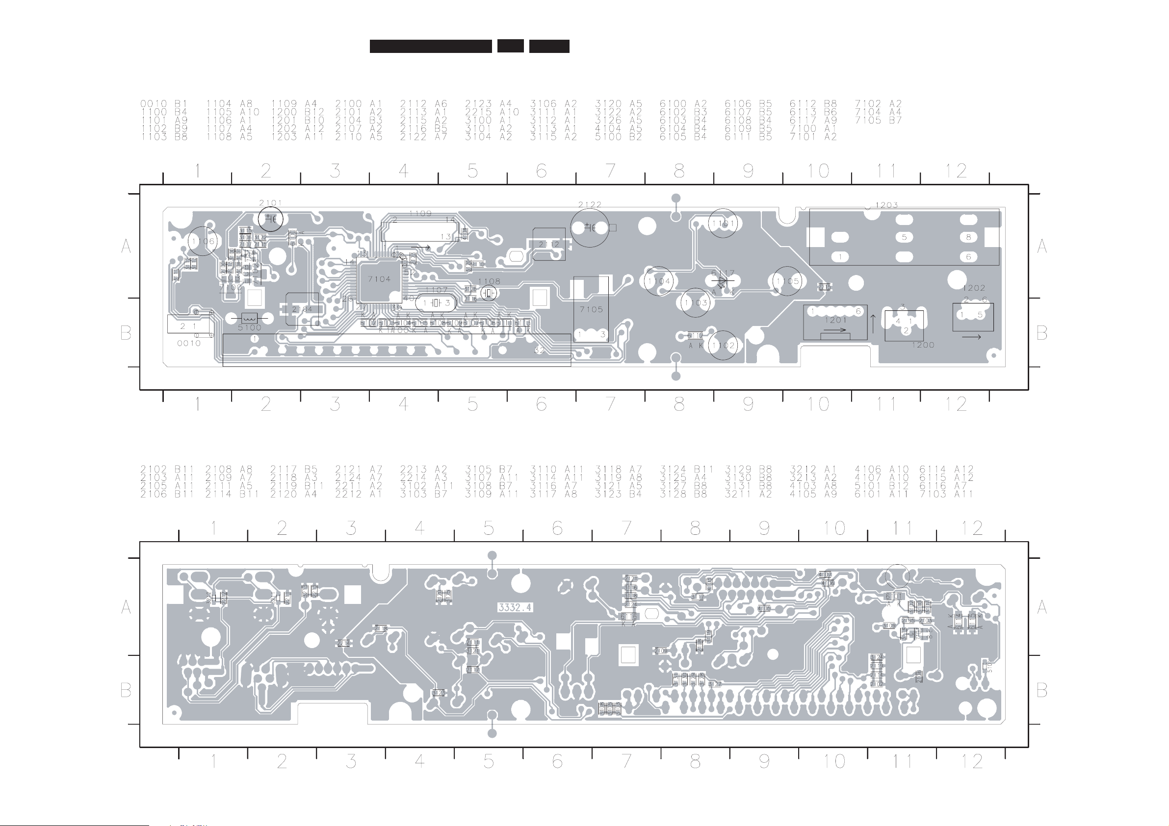
EN 29
3139 785 3220x
7.Circuit Diagrams and PWB Layouts
Layout: Front Panel (Top Copper Pattern) - SMD + Components
Layout: Front Panel (Bottom Copper Pattern) - Components
Front_Layout_3139_243_33312_pg1.pdf 2006-05-25
Front_Layout_3139_243_33312_pg2.pdf 2006-05-25
Page 30
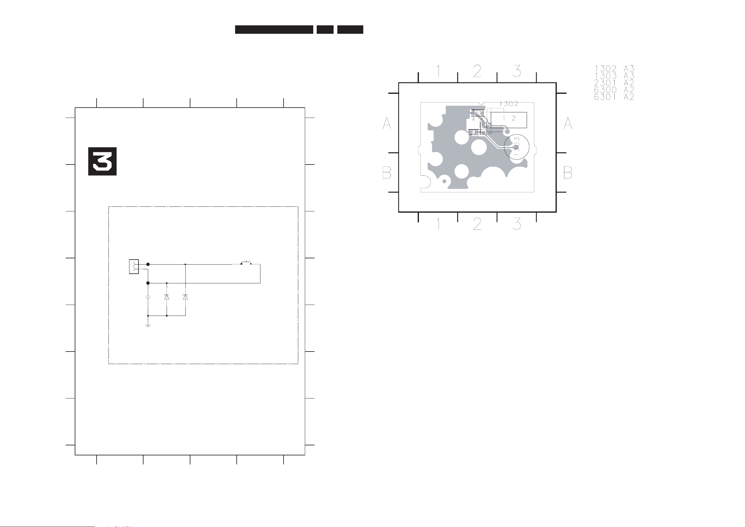
EN 30
3139 785 3220x
7.
Circuit Diagrams and PWB Layouts
Front: Standby
Layout: Standby (Top View)
Front_Layout_3139_243_33312_pg4.pdf 2006-05-25
A
B
12
DC0
34
1302 C1
1303 C4
2301 D2
6300 D2
6301 D2
F300 D2
F301 D2
I300 D3
A
B
C
D
E
F
1302
1
2
WH02D-1
F300
1032
GND
F301
C
1303
EVQ11L05R
8V6C-483XZB
2n2
8V6C-483XZB
0036
1036
D
E
F
G
3139_243_33314_130_3_a4.pdf 2006-02-28
12
3
G
4
Page 31
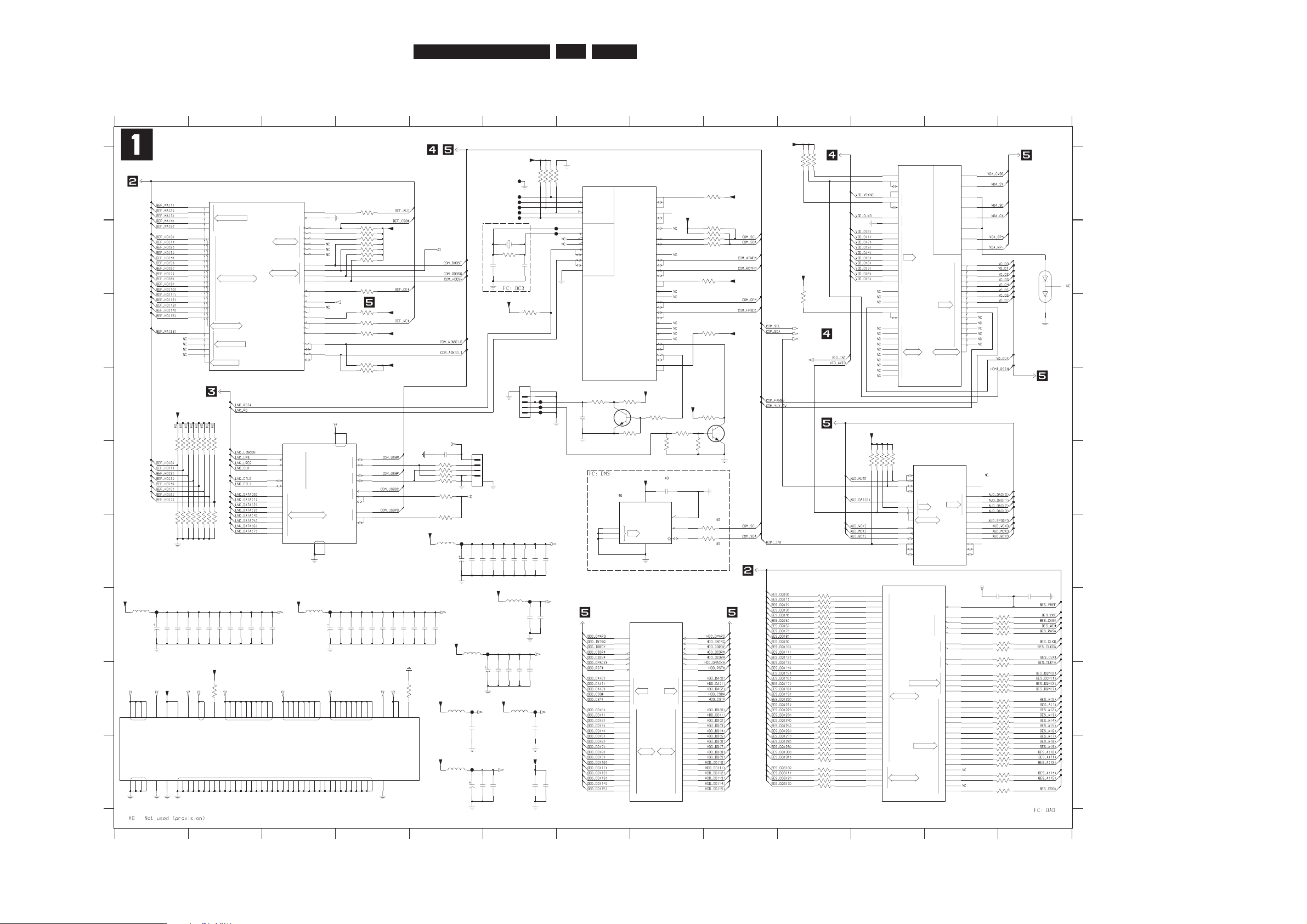
EN 31
3139 785 3220x
7.
Circuit Diagrams and PWB Layouts
Digital: Back-End Processor
3
2
1
0
DAC6_OUT
DAC5_OUT
1
0
1
2
3
4
5
GPIO<0:15>
VO_D
5
4
3
2
VO2_D
DAC1_OUT
DAC2_OUT
DAC2_OUTB
DAC3_OUT
DAC4_OUT
DAC4_OUTB
9
15
14
13
12
11
6
7
8
9
VO_HSYNC
VO_VSYNC
VO_ACTIVE
VO_E
1
0
6
7
GPIO29
PEC
GPIO45
VI_VSYNC
VI_CLK
VI_D
GPIO30 10
9
8
7
6
5
4
1
VI_E0
VI_E1
0
VO_CLK
0
8
4
5
0
1
1
0
0
0
RAS
WE
30
31
CAS
CKE
2
3
SDRAM_DQM
SDRAM_A
SDRAM_VREF
SDRAM
SDRAM_CLK
SDRAM_CLK
11
12
13
14
15
16
17
10
9
8
7
6
5
4
3
2
1
0
3
2
SDRAM_DQ
SDRAM_DQS
1
1
0
1
2
3
6
7
8
9
10
11
12
13
14
15
16
17
18
19
20
21
22
23
24
25
26
27
28
29
3
4
5
12
11
10
9
8
MDATA<0:15>
MADR<1:26>
HMST_ADRLO
4
3
2
1
0
HMST_UWE
HMST_RST
HMST_LDS
3
2
1
0
3
4
HMST_WAIT
2
1
0
HMST_CS0_8BIT
HMST_ALE
HMST_ADRDATA
HMST_ADRHI
HMST_CS
HMST_GPIO
HMST_OE
HMST_UDS
LWE
GPIO5
GPIO4
0
1
2
7
6
5
HMST_WR
HSMT_DTACK
PCMCIA_IOR
PCMCIA_IOW
4
3
2
1
0
15
14
13
LREQ
PHY_CLK
PHY_CTL0
PHY_CTL1
0
1
2
3
GPIO44
GPIO43
DMINUS
DPLUS
HOST_OC
HOST_PO1394_PHY_DATA
USB_AGND
USB_AVDD
1394
0
0
1
1
0
1
0
1
7
6
5
4
LINK_ON
LPS
SCL
ADR
0
1
2 SDA
WC
3
2
1
0
GPIO34
GPIO31
AI_D
GPIO<6:7>
AI_MCLKO
AI_MCLKI
AI_FSYNC
2
1
0
A2_SCLK
A2_FSYNC
AO_MCLKO
AO_MCLKI
AO_IEC958
AO_FSYNC
GPIO32
CS8
AO_D
GPIO33
CS9
AO_SCLK
AO2_D0
AI_SCLK
TRST
TMS
CLKI
CLKX
RSTO
EPD
CLK0_DAC
USB_48MHZ
CS10
GPIO42
GPIO41
TDI
TDO
TCK
BYPASS_PLL
SPI_CS3
SIO_UART1_CTS
SIO_UART2_TX
SIO_UART2_RTS
SIO_UART2_CTS
SIO_UART1_TX
SIO_UART1_RX
SIO_UART1_RTS
GPIO37
SIO_SPI_CS2
SIO_SPI_CS1
SIO_SPI_CS0
SIO_SPI_CLK
SIO_SDA
SIO_SCL
GPIO35
GPIO36
GPIO39
CS6
GPIO40
CS7
GPIO24
GPIO25
SIO_IRTX2
SIO_IRTX1
SIO_IRRX
SIO_UART2_RX
GPIO38
CS11
SIO_SPI_MISO
SIO_SPI_MOSI
15
12
13
14
INTRQ
IORDY
DIOR
DIOW
DMAACK
RESET
13
12
11
10
4
0
1
2
3
4
5
6
7
DMARQ
11
3
2
1
0
15
14
0
ADR
DATA
ADR
9
8
7
6
5
4
3
2
1
0
4
312
3
RESET
DMAACK
DIOW
DIOR
IORDY
INTRQ
DATA
9
10
8
DMARQ
00V
5
_
S
A
I
B
D
D
VF
E
R
VDDPVDD25
D
DV
_
S
ER
VDD
A9
1_
P
DD
V
FERV
DD
V
LA
T
X
AVDD
SUPPLY
AGND
1
_
SS
VD
_
CAD
SS
V
FE
R
GND
S
SV
L
A
TX
10V5_
S
A
I
B
D
DVD
_
CA
D
A80
_
PD
D
V
DAC_VDD
H
I
1101 B6
1105 E5
1111 D6
2101 B6
2102 B6
2105 E8
2106 E5
2108 G12
3456789101112
A
B
C
E
D
G
H
I
A
B
C
D
E
F
G
456789
2109 G13
2121 G3
2122 G4
2123 G4
Back-end Processor
Audio (AUD)
12
2124 G4
2125 G4
2126 G4
2127 G4
2128 G4
2129 G5
2130 G5
2131 G5
2135 I5
2141 F5
13
123
F
IEEE1394 Link - Physical (LNK)
2154 G1
2155 G2
2156 G2
2157 G2
2158 G2
2159 G2
2160 G2
2161 G2
2162 G3
2165 I6
10 11 12 13
2175 H6
2181 I5
2182 I5
2183 I6
2191 I6
2192 I6
2199 D7
3101 A6
3102 A6
3103 A6
2142 F5
2143 F5
2144 F6
2145 F6
2146 F6
2147 F6
2148 F6
2149 F6
2151 G1
2152 G1
2153 G1
3108 E5
3109 E5
3110 F5
3111 E11
3112 E11
3113 E11
3114 E11
3115 E11
3116 A10
3117 A10
2166 G6
2167 G6
2171 H5
2172 H6
Video Output Analog (VOA)
Back-end SDRAM (BES)
Back-end Flash (BEF)
2173 H6
2174 H6
3135 C4
3136 D4
3137 B4
3138 B4
3139 B4
3141 E1
3142 F1
3143 E1
3144 F1
3145 E1
3104 A6
3105 E5
3106 E5
3107 E5
)
DD
H
( e
vir
D
k
siD
d
r
a
H
3151 E2
3152 F2
3153 E2
3154 F2
3155 E2
3156 F2
3158 C6
3159 B8
3160 C8
3161 H2
3118 A10
3119 C10
3121 B4
3122 C4
3123 C4
3124 A4
3125 C4
3131 B4
3132 B4
3133 B4
3134 B4
3171-3 G10
3171-4 G10
3172-1 G10
3172-2 G10
3172-3 G10
3172-4 G10
3173-1 G10
3173-2 G10
3173-3 G10
3173-4 G10
3146 F1
3147 E2
3148 F2
3149 E2
3150 F2
3176-4 H10
3177-1 I10
3177-2 I10
3177-3 I10
3177-4 I10
3178-1 I10
3178-2 H10
3178-3 H10
3178-4 H10
3181-1 G13
3162 A8
3163 B6
3164 B8
3165 B8
3166 B8
3167 B8
3168 F9
3169 F9
3171-1 G10
3171-2 G10
3184-2 G13
3184-3 G13
3184-4 G13
3185-1 H13
3185-2 I13
3185-3 I13
3185-4 H13
3186-1 H13
3186-2 H13
3186-3 H13
3174-1 G10
3174-2 H10
3174-3 H10
3174-4 H10
3175-1 H10
3175-2 H10
3175-3 H10
3175-4 H10
3176-1 H10
3176-2 H10
3176-3 H10
3193 E8
3194 D8
3195 E8
3196 D7
3197 D8
3198 D7
3199 D7
5121 G3
5135 H5
5141 F5
3181-2 H13
3181-3 H13
3181-4 I10
3182-1 I10
3182-2 H13
3182-3 I10
3182-4 H13
3183-1 I10
3183-2 G13
3183-3 H13
3183-4 G13
3184-1 G13
7101-2 G8
7101-3 A12
7101-4 E12
7101-5 A2
7101-6 D3
7101-7 A7
7101-8 I3
7105 E8
7111-1 D7
7111-2 D9
3186-4 H13
3187-1 I13
3187-2 I13
3187-3 I13
Communication (COM)
)
DDO( e
v
i
r
D c
s
i
D
lacitpO
3187-4 H13
3188-1 I13
3188-2 I13
3188-3 I13
3188-4 I13
3191 H4
3192 D9
T113 G1
T114 G3
T115 G6
T116 G6
T117 H5
T118 H6
T119 I5
5151 G1
5165 G6
5166 H6
5171 G5
)DOV( latigiD tuptuO oediV
Video Input Digital (VID)
5181 I5
6101 B13
7101-1 F11
T101 A6
T102 A6
T103 A6
T104 A6
T105 A6
T106 A6
T107 B6
T108 B6
T109 D6
T110 D6
T111 D6
T112 F5
T116
T115
2106 100n
3185-122R 18
n0013812
452722R 3183-4
22R
22R 3183-2
3105
3106 22R
2K23413
T105
2K21413
K0
1
2113
3173-2 47R27
22R 18 3186-1
n0018512
n
0
019412 2013
0K1
T110
2K2
K0
13
11
3
65
1
3
BLM18P
5166
47R3175-3 3 6
BLM18P
5181
18
L24
H26
Y24
D22
AA26
47R3172-1
V25
V26
U25
U26
U24
N26
M26
K23
W25
R25
H23
G26
H25
H24
J24
J25
Y26
J23
J26
V24
W26
P26
N25
M25
M24
L26
L25
Y25
L23
K26
K25
K24
N23
P23
R23
T23
V23
W24
T25
T26
R26
P25
AB26
AA24
AC26
AB24
AD25
AD26
AE25
AC23
AF25
AA25
W23
AC25
AB23
AD24
AE26
AC24
AF26
AD23
AB25
Y23
7101-1
DMN-8652
Φ
SDRAM
K0
1
711
3
22R
3169
3159 4K7
22R
3176-1 47R18
3122
3168
22R
7
512
n001661
2
n001
B9
C8
B10
B11
A11
C11
C12
B12
A12
B13
A13B15
C18
A19
D18
C10
A16
A10
C13
C14
B14
A14
A15
C15
A20
A21
C20
B16
C16
D16
B17
C17
D17
B18
B19
B23
B22
A22
B21
C25
B26
C24
A26
B20 A3
A4
B4
A5
A6
B5
A7
A8
A17
A18
C19
6
7101-3
DMN-8652
DACVIDEO
Φ
3182-3 22R3
BLM18P
5135
3174-3 47R36
3165 22R
T119
T117
T118
u022
3198
1K0
18
V6
1
1812
47R3173-1
n
001
24
12
5121
BLM31
n001341
2
K
0
161
1
3
22R 3182-445
BC847BS
2
6
1
7111-1
5165
BLM18P
3109
3184-222R 27
10K
3183-1 22R18
45
n00
153
12
3186-422R
36
n
0
0172
1
2
3188-322R
n0
0
1271
2
27
2K29413
3181-222R
p811012
2K20513
T107
4K7
3197
27
K019113
47R3177-2
T112
AF9
T113 T114
AD8
AE14
AE10
AE9
AF13
AE18
AC17
AC10
AF14
AD10
AF10
AD9
AF7
AF15
AF16
AD12
AF17
AF18
AF19
AE5
AF5
AD13
AE15
AD14
AE11
AE7
AD7
AF6
AC8
AE6
AF8
AE8
AC9
AF12
AC11
AF11
AE12
AD11
AE16
AD15
AE17
AC16
AD16
Φ
HMST
7101-5
DMN-8652
AD17
AE13
K014113
9912
0n1
n
0
0
1
4
5
12
641
2
3187-422R 45
n001
K0
1
1
6
1
3
2 7 47R3176-2
n
00
103
12
XJ
1101
13M5
T109
%1
n0014712
27
1
913
2K1
3172-2 47R
n
0
0152
12
2K22513
0K14013
T103
BC847BS
5
3
4
7111-2
1
3
2
2109 100n
45
99VAB
1016
7
3181-4 22R
22R 3182-22
22R3121
BLM31
5151
T111
n0015612
n0010612
n
0015712
22R 36
22R 3188-445
3186-3
10K
3192
2K25513
5
913
8K6
22R3164
18
47R3178-1
3125 10K
n0
0
13
7
12
T102
10K3136
G4
G1
G3
3E
3F
4E
4F
3131 10K
M4
M3
J2
J1
K3
K2
E1
F1
E2
F2
G2
DMN-8652
7101-6
H3
L1
L2
K1
J4
L3
J3
L4
36
ANA
Φ
1394
22R 3181-3
7
17
1
2
V
52
u
01
47R3175-2 2
2K2451
3
2K
2
7
4
1
3
2K
2
5
4
1
3
36
3158
22R 3187-3
1412
V53u22
10K
p
812
0
12
45
K01
3
9
1
3
47R3177-4
n001
4
412
36
n
0
01
1
612
47R3172-3
T104
18
3123 10K
22R 3187-1
2K2841
3
3139 10K
u0
3
3
1
212
3175-1 1 8
V61
47R
36
n
0
01
4
212
3176-3 47R
6
3194
10K
47R3178-3 3
n0012212
3138 10K
100n
2105
3183-322R 36
3186-222R 27
3162 10K
n0
0
12
5
12
84
7
(2Kx8)
Φ
EEPROM
7105
M24C16-RDW6
1
2
3
6
5
36
n
0
01
1
312
45
3177-3 47R
3172-4 47R
n
00
1
95
12
2K21513
36
10K
3185-322R
W2
R1
Y1
3133
P3
N3
N2
M2
M1
N1
W3
T3
V1
V4
P1
U3
U1
P2
R3
T2
U2
V2
W4
T1
R2
AD5
AD4
AF3
AC5
AF4
AE4
AD6
Y2
W1
V3
U4
AE1
AF1
Y4
AA2
AB1
AA3
AB2
AC1
AB3
AC2
AE2
AD3
AC4
AF2
AE3
Y3
AA1
AD1
AB4
AC3
AD2
7101-2
ATAPI2ATAPI
Φ
DMN-8652
n0018412
3137 10K
n0018212
n
0
01761
2
n
00
1
26
12
4K7
18
3166
3513
3177-1 47R
2K2
18
4K73160
22R3182-1
n001741
2
3199
100R
AE23
AD20
B8
A9
B7
D8
C7
H2
AC18
AD22
AE22
AE20
AF23
AC20
AF24
AC22
AE24
AF22
D9
C9
AE19
AD19
AF20
AD21
AC19
AD18
AF21
AE21
7101-7
DMN-8652
SERIAL_IO
MISC
JTAG
H4
H1
A1
A2
F26
G25
E25
A23
B25
A25
F24
Φ
E23
D26
E24
E26
C26
B24
A24
D24
F25
G24
G23
DMN-8652
AUDIO
Φ
7101-4
D25
47R36
3171-3
4522R 3185-4
5171
BLM18P
3188-122R 18
3184-422R 45
27
5
5
12
3187-222R
22R 18
n
00
1
3184-1
T106
n
0
01
3
512
453178-4 47R
n0016212
n001281
2
2K24413
2K22413
3108 15K
n
0013212
BLM31
5141
1
2
3
4
56
1111
B4B-PH-SM4-TBT(LF)
n00
1
54
1
2
47R3174-4 4 5
22R 3185-227
183174-1 47R
32F
4K
4N
4AA
6
CA12C
A
3
2A
A
1
C
1
B
2B
4
P
4R
4T
31
C
A
21
C
A
4
1
CA
51
C
A
1
1
D21D
3
1D
2
2C
3
2
M
42N
42P
42R
42T
32U
41D
51D
91D
0
2D
6
1
T
2
1
L
3
1
L
4
1
L
5
1
L
6
1
L
1
1
M
1
D
2
C
01D
3
2D
31
R
1
1
L
4
1R
51R
6
1
R
11T
21T31T41T
5
1
T
5
1N
3
2C
6
1
N
1
1P21P31
P
41
P
5
1P
61P
1
1
R21R
6D
1
2C
2
1
M
3
1
M
4
1
M
5
1
M
6
1
M
11N2
1
N
3
1N41N
4C
5D2D3D
4D12D
7
CA
7D6B6
C
DMN-8652
7101-8
5C
3C
3B
3132 10K
2722R 3188-2
15K3107
47R3171-4 4 5
n0012
9
12
5
T108
3175-4 47R4
V
5
2
u
0
1
1512
3178-2 47R27
22R 3181-118
22R3124
4K7
3196
n0011912
1847R3171-1
3135 10K
5
10K3110
3173-4 47R4
K011113
47R3173-3 3 6
3163
1M0
B4B-PH-SM4-TBT(LF)
1
2
3
4
56
1105
n
0
01
6
512
27
27
47R3174-2
3171-2 47R
2K2641
3
K01
K018113
5113
0K11013
10K3134
T101
22R 3184-336
n0019212
4K73167
0K13013
47R3176-4 4 5
100n2108
VIP_RST#
BEF_OE#_1
5V
5V
5V
1V8BE
2V5BE
COM_SCL_1
COM_SDA_1
TCK
TDI
TDO
TMS
TRST#
SYSRST#
BES_DQM(1)_1
BES_DQS(2)_1
VIP_SCL
VIP_SDA
3V3A
VIPINT
VIPINT
COM_USBP1
USBP1
USBM1
2V5S
BEF_WE#_1
BEF_ALE_1
3V3BE
3V3BE
3V3BE
3V3BE
3V3BE
3V3BE
3V3BE
3V3BE
3V3BE
3V3U
3V3BE
5VBE
3V3BE
3V3BE
3V3BE
3V3P
3V3BE
BES_DQ(14)_1
BES_DQ(12)_1
BES_A(7)_1
3V3BE
BES_DQ(28)_1
BES_DQ(29)_1
BES_DQ(30)_1
BES_DQ(31)_1
BES_DQ(24)_1
BES_DQ(25)_1
BES_DQ(26)_1
BES_DQ(27)_1
BES_DQ(20)_1
BES_DQ(21)_1
BES_DQ(22)_1
BES_DQ(23)_1
BES_DQ(16)_1
BES_DQ(17)_1
BES_DQ(18)_1
BES_DQ(19)_1
BES_DQ(13)_1
BES_DQ(15)_1
BES_DQ(8)_1
BES_DQ(9)_1
BES_DQ(10)_1
BES_DQ(11)_1
BES_DQ(4)_1
BES_DQ(5)_1
BES_DQ(6)_1
BES_DQ(7)_1
BES_DQ(0)_1
BES_DQ(1)_1
BES_DQ(2)_1
BES_DQ(3)_1
BES_A(14)_1
BES_A(0)_1
BES_DQM(0)_1
BES_CAS#_1
BES_DQM(2)_1
BES_DQS(1)_1
BES_A(10)_1
BES_A(5)_1
BES_CLK1_1
BES_CLK1#_1
BES_DQS(3)_1
BES_DQM(3)_1
BES_A(15)_1
BES_A(8)_1
BES_CS0#_1
BES_A(3)_1
BES_CKE_1
BES_A(1)_1
BES_A(12)_1
BES_RAS#_1
BES_WE#_1
2V5S1V8C 3V3P3V3A
3V3BE
3V3P
COM_USBM1
3V3U
3V3A 5VBE 1V8D 3V3V 3V3R
1V8C
1V8BE
3V3BE
3V3R
3V3BE
3V3V
3V3BE
1V8D
3V3BE
2V5S
3V3BE
5VBE
3V3BE
BES_CLK0#_1
BES_CLK0_1
BES_DQS(0)_1
BES_A(11)_1
BES_A(2)_1
BES_A(6)_1
BES_A(4)_1
BES_A(9)_1
3139_243_34464_130_01_a2.pdf 2006-03-20
Page 32
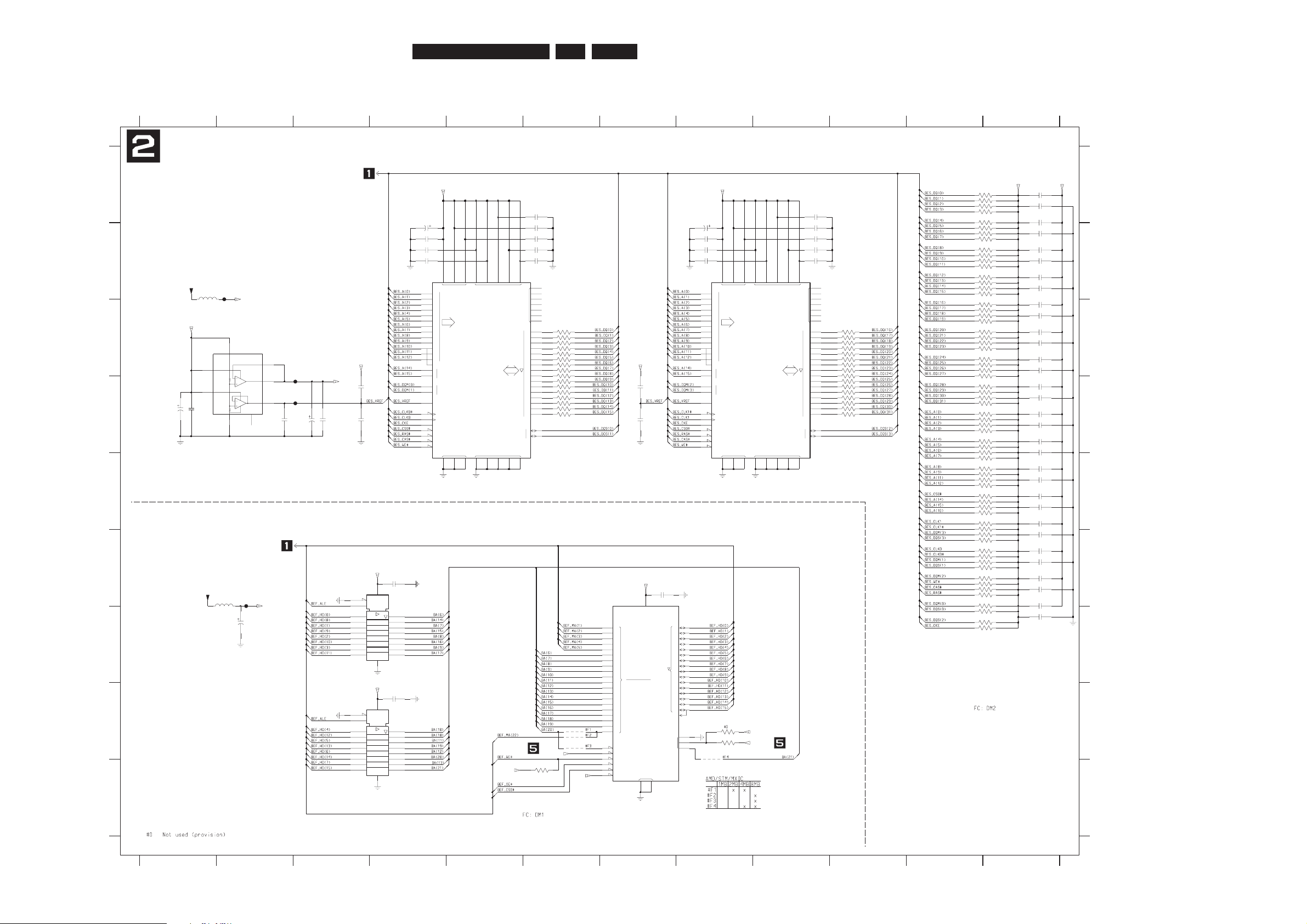
EN 32
3139 785 3220x
7.Circuit Diagrams and PWB Layouts
Digital: Memory
EN
C1
1D
19
0
1
2
3
4
5
6
7
8
9
10
11
12
13
14
15
16
17
18
19
VSS
VDD
0
A
D
5
2
4
RB
OE
CE
7
6
WE
3
1
RP
0
BYTE
2M-1 / 1M-1
NC
A-1
8
9
10
11
12
13
14
15
D
A
DQS
L
U
11
4
5
6
1
2
3
CK
DM
U
L
VREF
10
CK
4
BA
CS
512
2
CAS
WE
15
RAS
0
CKE
VSS
9
14
13
VSSQ
VDDQVDD
7
1
0
NC
6
12
8
1
0
10
11
AP
3
7
8
9
D
A
DQS
L
U
11
4
5
6
1
2
3
CK
DM
U
L
VREF
10
CK
4
BA
CS
512
2
CAS
WE
15
RAS
0
CKE
VSS
9
14
13
VSSQ
VDDQVDD
7
1
0
NC
6
12
8
1
0
10
11
AP
3
7
8
9
EN
C1
1D
67
2202 D1
Back-end SDRAM (BES)
89101112
12
2211 A4
2205 D2
2204 D3
2203 D3
2201 D1
I
2212 B4
2213 B4
345
3267-4 D11
3269-1 E11
3269-2 D11
3269-3 D11
3269-4 D11
3255-3 B11
3255-4 B11
3257-1 B11
3257-2 B11
3257-3 B11
3257-4 B11
3259-1 C11
3259-2 C11
3259-3 C11
3259-4 C11
3261-1 C11
6453
3253-2 B11
3253-3 B11
3253-4 A11
3255-1 B11
3255-2 B11
2284 G12
2291 G2
2292 F4
2293 H4
2294 F7
3231-1 C6
3231-2 C6
3231-3 C6
3231-4 C6
3233-1 C6
3233-2 C6
3267-3 D11
3275-2 F11
4292 H6
4293 H6
4294 H8
5201 B1
3271-1 E11
3271-2 E11
3271-3 E11
3271-4 E11
3273-1 E11
3273-2 E11
3245-1 D10
3245-2 D10
3245-3 D10
3245-4 D10
3251-1 A11
3251-2 A11
3251-3 A11
3251-4 A11
3253-1 B11
2255 B12
2256 B12
2257 B12
2258 B12
2259 C12
G
H
I
A
B
C
D
E
F
G
H
Back-end Flash (BEF)
3273-3 E11
3275-3 E11
3273-4 E11
3275-1 F11
2277 F12
2278 F12
2281 F12
2282 F12
2283 F12
2238 B9
2239 B9
2240 D7
2241 D7
2251 A12
2252 A12
2253 A12
2254 B12
B
C
D
E
F
2236 B9
2237 B9
12
Memory
2271 E12
2272 E12
2273 E12
2274 E12
2275 E12
2276 F12
3261-2 C11
3261-3 C11
3239-2 C10
3239-3 C10
3239-4 C10
3241-1 C10
3241-2 C10
3241-3 C10
3241-4 C10
3243-1 C10
3243-2 D10
3243-3 D10
3243-4 D10
789101112
A
3277-1 F11
3277-2 F11
3277-3 F11
3277-4 F11
3281-1 F11
3261-4 C11
3263-1 C11
3263-2 C11
3263-3 C11
3263-4 C11
3265-1 D11
3265-2 D11
3265-3 D11
3265-4 D11
3267-1 D11
T204 F2
3281-2 F11
3281-3 F11
3281-4 F11
3283 F11
3284 G11
3285 G11
3286 G11
3294 H8
3295 I6
3296 H8
4291 H6
3267-2 D11
3275-4 E11
2261 C12
2262 C12
2263 C12
2264 C12
2265 D12
2266 D12
2267 D12
2268 D12
2269 D12
2270 D12
5291 F2
7201 C1
7211 C5
7231 C9
7292 F3
7293 H3
7294 H7
T201 D3
T202 D3
T203 B2
7
2214 B4
2215 A6
2216 B6
2217 B6
2218 B6
2219 B6
2220 D3
2221 D3
2231 A8
2232 B8
2233 B8
2234 B8
2235 A9
3233-3 C6
3233-4 C6
3235-1 C6
3235-2 D6
3235-3 D6
3235-4 D6
3237-1 D6
3237-2 D6
3237-3 D6
3237-4 D6
3239-1 C10
2260 C12
47R3275-2 2
47R3277-2 2 7
18
3281-1 47R
1
19
18
17
16
15
14
13
12
02
2
3
4
5
6
7
8
9
01
11
5
7292
74LVC573APW
3251-4 47R4
4291
100n2234
47R3283
2275 100n
47R3257-3 3 6
100n2272
2219 100n
100n2218
100R 3243-3
100R 3243-2
100R 3243-1
3241-1
100R
100n
2293 100n
2264
45
47R3265-4
3253-4 4 5 47R
2292 100n
27
47R3281-2 2 7
47R3261-2
18
47R3271-1
100R 3237-4
100R 3237-3
3237-2100R
100R 3237-1
100R 3235-4
100R 3235-3
100R 3235-2
100n2236
100R 3245-4
100R 3245-3
100R 3239-1
100R 3239-2
100R 3239-3
100R 3239-4
3235-1100R
100R 3233-1
100R 3233-2
100R 3233-3
100R 3233-4
100R 3231-4
100R 3231-3
47R3251-3 3 6
2267 100n
100n2256
2255 100n
3277-3 47R36
27
3251-2 47R 2252 100n
3245-2
100R
100R 3245-1
100R 3243-4
36
47R3273-3
100R 3231-2
n001
100R
3231-1
0422n0011422
13
14
10
28
15
12
7
3
72
6
4
11
43
45
33
35
38
40
42
44
30
32
18
8
7
47
26
29
31
34
36
39
41
1
48
17
16
9
23
22
21
20
19
M29W160ET70N6F
7294
25
24
6
5
4
3
2
2Mx8/1Mx16
[FLASH]
100R 3241-2
100R 3241-3
100R 3241-4
47R363269-3
T201
5201
100n2262
BLM31
8
5
46
21
n
0012022
5
5
16
49
43
84
66
6
21
25
50
53
23
47
51
1
81
33
3
9
51
13
54
56
20
16
14
17
19
25
43
57
59
60
62
63
65
5
7
8
10
11
40
26
27
22
45
44
46
24
2
4
30
28
41
42
31
32
35
36
37
38
39
SDRAM
16Mx16
Φ
DDR
7231
29
V53u22
1022
3296 4K7
100n2278
2239 100n
2266 100n
7
2237 100n
3257-2 47R2
21
258546
21
3
339
51
55
16
49
438466
6
19
25
43
50
53
23
47
51
1
8
1
8
10
11
13
54
56
20
16
14
17
24
2
4
57
59
60
62
63
65
5
7
36
37
38
39
40
26
27
22
45
44
46
7211
DDR
29
30
28
41
42
31
32
35
SDRAM
Φ
16Mx16
35V22u
2235
2231
n
001
40
2
2
100n
47R3265-2 2 7
2274 100n
47R3285
1922
V
52u01
5291
BLM18P
183267-1 47R
3275-4 47R45
47R3273-4 4 5
45
8
3257-4 47R
3277-1 47R1
47R18
2273
3255-1
100n
2261 100n
22u 35V
2211
2212 100n
3286
47R
27
100n2281
8
3267-2 47R
47R3263-1 1
47R3269-4 4 5
47R45
3277-4
2238 100n
2283
3281-3 3 6
100n
47R
100n2232
2270 100n
2271 100n
4294
8
3259-1 47R1
47R3271-3 3 6
2260 100n
47R3263-3 3 6
3265-3 47R36
27
10K
47R3273-2
3261-3 47R36
3295
2214 100n
14
13
12
02
8
9
01
11
1
19
18
17
16
15
7293
74LVC573APW
2
3
4
5
6
7
100n2294
100n2277
4K73294
3269-2 2 7 47R
2233 100n
47R27
100n2251
3255-2
100n2284
V
6
1u0
33
3022
45
18
3263-4 47R
3265-1 47R
47R3281-4 4 5
7
T202
3263-2 47R2
2258 100n
47R3257-1 1 8
100n2259
100n2269
n0011222
47R3251-1 1 8
100n2265
100n
47R3275-1 1 8
2213
47R18
100n
3269-1
47R36
2253
27
3259-3
47R3259-2
100n2217
4292
3271-2 47R27
100n2257
47R3261-4 4 5
100n2276
5 47R3267-4 4
3267-3 47R36
2254
3261-1 47R18
100n
47R3259-4 4 5
45
3253-1 47R18
3255-4 47R
2215 100n
3273-1 1 8
n
0
01
5
0
2
2
47R
47R36
2263 100n
27
3253-3
45
47R3253-2
3271-4 47R
2216 100n
3284 47R
100n2268
3255-3 3 6
2282 100n
47R
4293
47R3275-3 3 6
T204
4VREF
3VSENSE
8VTT
T203
6 AVIN
2
DNG
C
N
1
7 PVIN
5Q
D
DV
n0
0
10
2
22
LP2995
7201
2V5D
2V5D
VTT
3V3F
SYSRST#
2V5BE
3V3F
2V5D
VTT
2V5D
2V5D
3V3BE
3V3F
3V3F
3V3F
SYSRST#
2V5D
2V5D
3V3F
3V3F
BA{BA(6:21),BEF_HD(0:15)}
3139_243_34464_130_02_a2.pdf 2006-03-20
Page 33
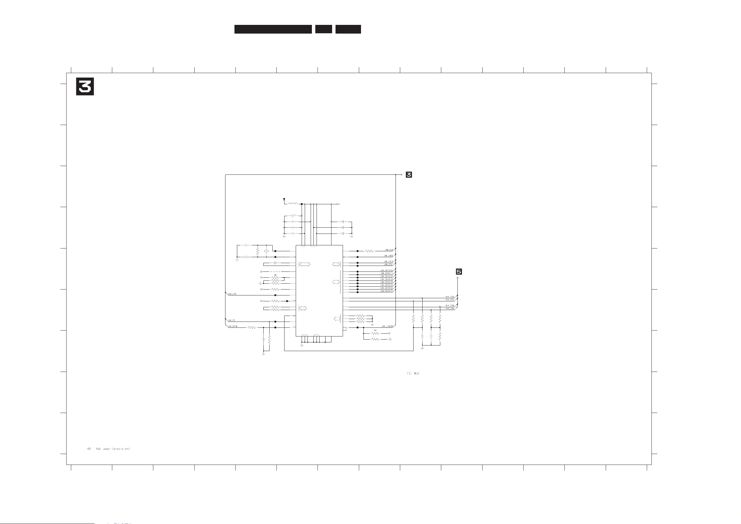
EN 33
3139 785 3220x
7.
Circuit Diagrams and PWB Layouts
Digital: IEEE 1394 Physical Layer
0
1
R
0
1
FILTER
DGND
LKON
D
PC
CTL
DDVLLP
S
H_
D
N
G
AGND
DVDD
DNGLLP
AVDD
TPA+
TPA-
TPB+
TPB-
7
6
5
4
3
2
1
0
1
0
LREQ
SYSCLK
RESET
PD
TPBIAS 0
1
C
2
XO
ISO
LPS
TESTM
SE
SM
CPS
XI
G
H
I
A
B
IEEE1394 Physical Layer
)YHP( tro
p
snarT
laci
s
yhP 4931E
E
EI
14
A
B
C
D
E
F
11 12 13 14
1
C
D
E
F
G
H
I
1351 D5
2301 D6
12345678910
2321 G5
2341 G9
2343 G9
2351 D5
2352 E5
234567
3332 F5
3341 F9
3342 F9
3343 F9
3344 F9
8 9 10 11 12 13
2302 D6
2303 D6
2304 D6
2305 D7
2306 D7
2307 D7
2361 E5
3301 E5
3302 F5
3303 G8
3304 G8
3305 E8
3306 F7
3307 F7
3308 F7
3321 F5
3322 G5
3331 F5
T308 F7
T309 E7
T310 F6
T311 F7
T312 E7
3345 G9
3351 E5
3360 E5
3361 E5
3362 E5
4361 E5
IEEE1394 Link - Physical (LNK)
T313 E7
T314 E7
T315 F6
T316 F6
T317 C6
T321 F6
T351 E6
T352 E6
5301 C6
7301 D6
T301 E7
T302 E7
T303 E7
T304 E7
T305 E7
T306 E7
T307 E7
3304 10K
5301
BLM18P
T311
24
33
n
001
12
32
%
1R
65
T307
T321
T312
T305
27
31
42
43
1K03301
33
34
37
23
24
1
22
30
29
28
9
4
19
13
48
16
17
1812
14
04
10
11
416474
1
2
44
54
38
39
53
20
2
3
15
4
5
6
7
8
9
1-PORT CABLE
TSB41AB1PHP
7301
6
2
23
63
52
TRANCEIVER
ARBITER
Φ
p
02
2
343
2
0M1
1533
T301
%1
3433
24M576 AT-51CD2
1351
R6
5
7
K4
100n2305
22
3
3
2302
T316
100n
T315
3306 680R
T314
680R3307
4361
T304
T308
%11K
5
5433
2303 100n
0u1
T351
T352
14
3
2
3362 1K0
T303
10K3303
1K03361
T310
2352 33p
25V10u
2301
100n2304
3302 10K
750R3332 1%
1%5K63331
R6
5
4433
%1
1K03360
T317
T302
R65
1
433
%
1
100n2361
T309 3305 22R
100R3321
2306 100n
T313
T306
2307 100n
3308 680R
33p2351
3V3I
3V3I
3V3BE
3V3I
3V3I
3V3I
3V3I
3139_243_34464_130_03_a2.pdf 2006-03-20
Page 34
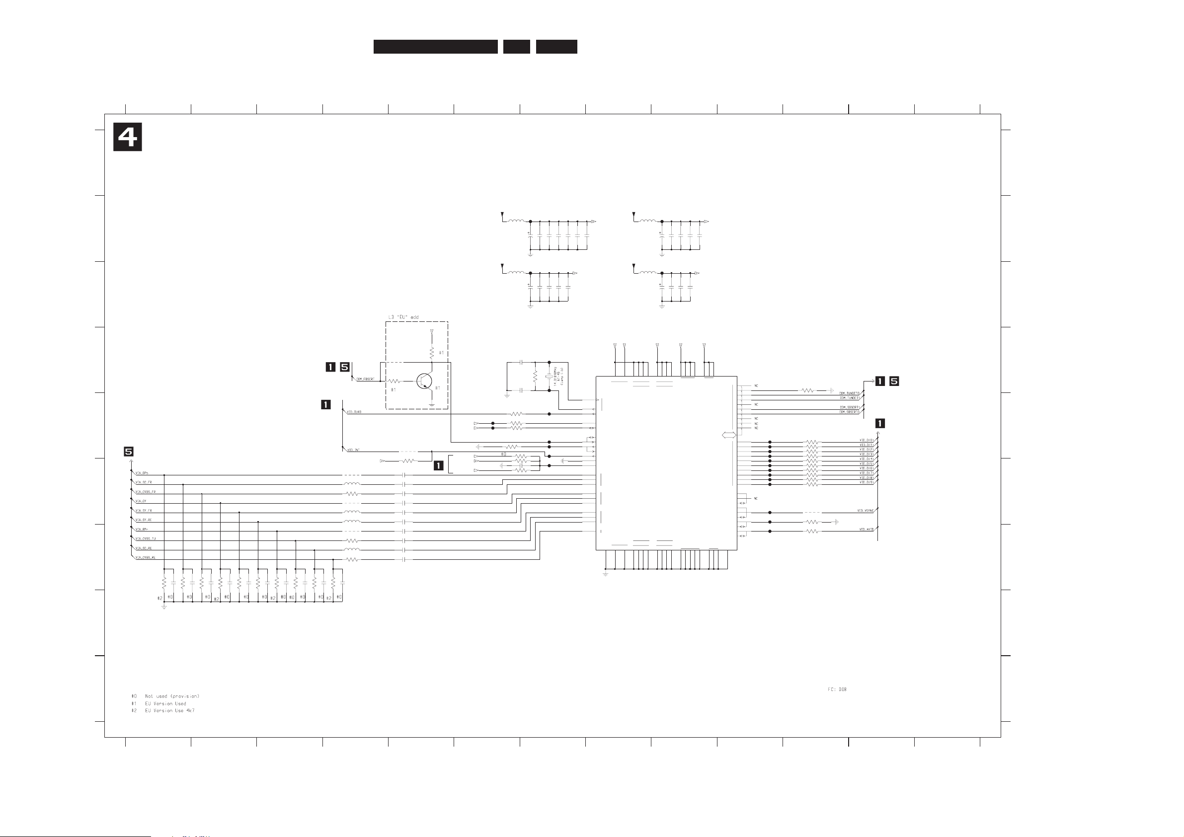
EN 34
3139 785 3220x
7.Circuit Diagrams and PWB Layouts
Digital: Video Input Processor
A18VDD
23
CS
9
8
GPIO
C_
7
SDA
SCL
A
C
A
2
1
0
VI_4
VI_3CB
GND_HSDGND
2
A33GND
CH
43
C
VI_2
XTAL
IOGND
8
Y_
GPIO
6
5
4
3
34
A18GND
CH
A18GND
1
VBLK
GPIO
GPIO
GPIO
DATACLK
2
1
5
2REF PLL
B
A
GLCO
FSS
234
CH
A33VDD
IOVDD
1
2
3
GPIO
9
RESETB
PWDN
INTREQ
I2CA
VI_1
A
B
6
7
REF
AVID
4
HS
VS
FID
AGND 1
4
CH
A18VDD
11
DVDD
0
PLL
2414 B9
2415 B9
2421 B7
2422 B7
2423 B7
2424 B7
6 7 8 9 10 11
)
D
I
V
(
lat
i
giD tupnI
o
ediV
H
I
1461 D7
2401 C9
2402 C9
2403 C9
2404 C9
2411 B9
2412 B9
2413 B9
8 9 10 11 12 13
12345
B
C
D
E
F
G
12 13
1234567
2462 D7
2471 F5
2472 F5
2473 F5
2474 F5
2475 F5
A
B
C
D
E
F
G
H
I
A
2483 G2
2484 G2
2485 G2
2486 G3
2487 G3
2488 G3
Video Input Processor
Communication (COM)
2425 B7
2426 B7
2427 B8
2431 C7
2432 C7
2433 C7
2434 C7
2435 C7
2453 F6
2461 D7
3453 F6
3454 E7
3455 E6
3456 F11
3457 D11
3461 D7
)DIV( latigiD tupnI oediV
)
A
IV( gol
anA tu
pn
I oedi
V
2476 F5
2477 G5
2478 G5
2479 G5
2480 G5
2481 G1
2482 G2
3476 H2
3477 H3
3478 H3
3479 H3
3480 H4
3481 F5
3484 F11
3486 F11
3488-1 F11
2489 G4
2490 G4
3407 E6
3408 E6
3423 F4
3428 G4
3430 G4
3450 D5
3451 G11
3452 F6
3488-2 F11
3488-3 F11
3488-4 F11
3492-1 E11
3492-2 E11
3492-3 E11
3492-4 E11
3494 D5
4481 E5
5403 F4
5404 F4
5405 G4
3471 H1
3472 H1
3473 H2
3474 H2
3475 H2
T402 E10
T403 E10
T404 F10
T405 F10
T406 F10
T407 F10
T408 F10
T409 F10
T411 E7
T412 E7
T413 B7
3482 E7
T422 E6
T423 F7
T431 G10
T432 F10
T433 E7
T434 F10
T435 E7
T461 D7
T462 E7
4482 F4
4483 F4
4484 G4
4486 F11
4487 D5
5401 C8
5402 F4
5411 B8
5421 B6
5431 C6
7401 E9
7402 D5
T400 E10
T401 E10
Communication (COM)
T414 C7
T415 B9
T416 C9
T421 E6
100R
3455
100n2453
4487
K
01
05
4
3
100R
3494
100n
BC847B
7402
2476
22R3488-1 1 8
22R3451
T402
4482
%1R575743
270R
3423
5431
BLM18P
5403
600R
T461
4342
T435
n
0
0
1
n
0
01
534
2
%127
4
3R
5
7
T422
6
0M
1
1643
3492-3 22R3
n
0012
1
42
n00
13
142
n0
01
2042
4481
T433
T412
T411
T431
T408
3492-1 1 8
T409
T405
22R
4486
T400
3484
22R
n0016242
3430
270R
4484
p00
18
842
7
24
2
p00
1
4
8
42
3492-2 2 7
n001
22R
p00
15
84
2
100n2474
3457
2473 100n
2K2
p
0016842
22R
3408
34542K2
%10843
T401
R57
%1R
57
9
74
3
T462
T416
T421
T415T413
T414
2471 100n
T423
n001
T406
22R3492-4 4 5
4142
T432
T403
R
5
7%137
4
3
%
1R
5
717
4
3
5421
BLM18P
n
0
0
13
2
4
2
3453
100R
6
743
T407
%1R57
094
2
348110K
p
001
100n2475
3407
22R
n0
0
1
33
4
2
n001
3
042
n0012342
1042
V5
2
u0
1
3456 2K2
1142
V5
2
46
45
44
43
u01
18
23
73
74
75
54
53
52
51
50
47
28
29
80
1
2
7
8
9
16
17
30
9
3
9426
83
8
4
16
77 67
33
34
86
13
14
5
5
76
71
35
37
1
8
72
64
63
60
59
58
57
40
7
2
2
3
2
4
65
41
9
1 02
4
2 5
2
22 12
70
69
66
65
36
9
7 8
7
3 4
0
1
11
6
5
51
L2146PFP
7401
Φ
NTSC/PAL/SECAM
VIDEO DECODER
3
1 21
6
2
1
3
42
V52
u
0
1
600R
5405
100n2480
100n2478
2479 100n
2477
3488-2 22R27
100n
270R
3428
600R
5402
4483
600R
5404
100n2472
R5
7
4
7
4
3
7743
%1
n
00142
4
2
%1R
5
7
2462
33p
n0015142
p
00
12
8
4
2
5401
BLM18P
p00138
4
2
453488-4 22R
1242
V61u03
3
p001
9
842
5411
BLM18P
p
00178
4
2
36
T404
R5
7
22R3488-3
%
18
743
22R
3486
n
0012242
22R 3482
10K3452
2461
33p
n0015242
1641
n0014042
T434
3V3D2
3V3D2
p
0
0
1
1
8
4
2
VIA_CVBS_RE_3
VIA_SC_RE_3
VIA_CVBS_TU_3
VIA_RPr_3
VIA_SY_RE_3
VIA_SY_FR_3
VIA_GY_3
VIA_CVBS_FR_3
VIA_SC_FR_3
VIA_BPb_3
VIA_SC_RE_2
VIA_RPr_2
VIA_CVBS_RE_2
VIA_CVBS_TU_2
VIA_SY_RE_2
VIA_GY_2
VIA_SC_FR_2
VIA_SY_FR_2
VIA_CVBS_FR_2
VIA_BPb_2
1V8BE
2A8V
1
VIP_RST#
3V3D2
SYSRST#
VIP_SCL
VIP_SDA
1V8BE
1V8A2
1V8D2
3V3BE
3V3D2
3V3BE
3V3A2
2A8V1
2D3V3
2D8V1
2
A
3V3
3139_243_34464_130_04_a2.pdf 2006-03-20
Page 35
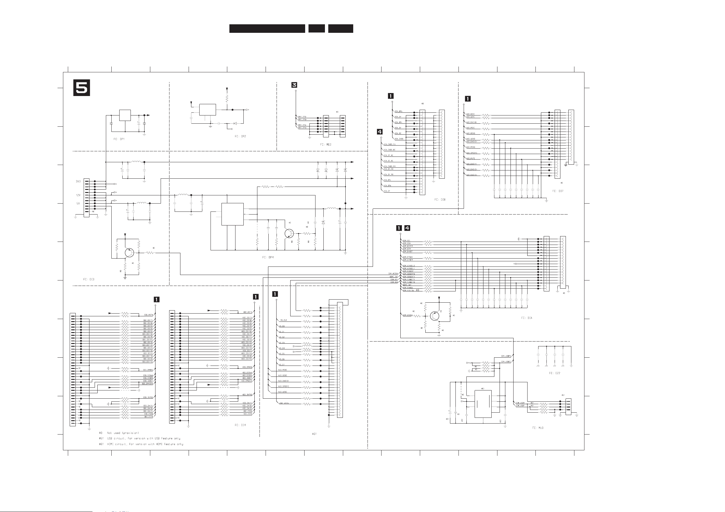
EN 35
3139 785 3220x
7.
Circuit Diagrams and PWB Layouts
Digital: Interfaces
COM
OUTIN
1
2
IN
1
23OUT
FB
OUT
COMP
VREFVCC
INH
SYNC
GND GND_HS
5
1522 A10
1536 A13
1537 C13
1541 F7
1551 D13
1552 D13
A
B
C
D
E
4581 H2
4624 H11
3590 H6
3591 H6
3592 H6
3593 H6
3594 H6
12 13
H
I
A
B
C
D
E
10 11 12 13
1234
T576 G1
)YHP( tropsnarT - lacisyhP 4931EEEI
T531 C9
T532 C9
T533 C9
T534 C9
T535 C9
F
G
2508 H13
2511 D2
2512 D2
2513 D2
2515 A2
2516 B1
2517 B2
3681 H4
3682 H4
3683 I4
3684-1 I4
3684-2 I4
3684-3 I4
3684-4 I4
4523 D5
2625 I10
2683 I4
1571 F1
1671 F3
2502 I12
2503 I11
2505 H13
2506 H13
2507 H13
2567 F12
2583 I2
3595 A4
3596 I6
6501 C7
6502 C7
6505 C7
6506 C7
6521 D7
6595 A5
7501 H11
T566 F13
T567 F13
T568 F13
T571 F1
T572 F1
T573 G1
T574 G1
T575 G1
3672 F4
3673-4 F4
3673-1 G4
3673-2 G4
3589-3 H6
3589-4 H6
Communication
3567 E10
3568 F10
3569 F10
3570 G10
3571 F2
3572 F2
3597 I6
T536 A13
T537 A13
T577 G1
T578 G1
T579 G1
T580 G1
T581 G1
2556 F11
2557 F11
2558 F12
2559 F12
2561 F12
2596 A4
2626 I10
HDMI
3584-4 I2
3584-3 I2
ODD_IDE
3584-1 I2
3544 B11
3545 B11
3546 C11
3547 B11
3548 B11
3581 H2
2595 A4
T688 H3
T689 H3
3588-1 G6
3588-2 G6
3588-3 G6
3588-4 G6
3589-1 G6
3589-2 G6
3673-3 G4
IEEE1394
Interfaces
78
6 7 8 9 10 11
3
3671 F4
2548 C12
2549 C12
2552 F11
2553 F11
3575-3 G2
3575-4 G2
3576-1 G2
3576-2 G2
3576-3 H2
3576-4 H2
3584-2 I2
)DD
O
( ev
i
rD cs
i
D
la
ci
t
pO
T542 B13
Power supply
T543 B13
T544 B13
4681 H4
5511 C2
5513 G6
5514 G6
5518 B2
5521 C3
5525 D7
T538 A13
3582 I2
3583 I2
3585 F6
3586 F6
3587 G6
I
1501 C1
1502 H13
1511 A7
1512 A7
1521 A10
9
T599 I1
T605 I13
T600 I1
T555 E13
T556 E13
T557 E13
T558 E13
T596 I1
456
3574-4 G2
3575-1 G2
3575-2 G2
T525 B9
T526 B9
T527 B9
T528 B9
T529 C9
T530 C9
T695 H3
T694 H3
T692 H3
T696 I3
T620 F7
T621 F7
T690 H3
T539 A13
T540 B13
T541 B13
F
G
H
T585 G1
T586 G1
T587 H1
T588 H1
T589 H1
T590 H1
T601 I1
T598 I1
)D
U
A
( o
i
d
u
A
T626 G7
T624 G7
T628 G7
)MOC( noitacinummoC
T627 G7
HDD_IDE
T622 F7
T597 I1
T522 B9
T523 B9
T524 B9
T677 G3
T678 G3
T679 G3
T680 G3
T681 G3
T682 G3
T693 H3
T641 I7
T673 F3
T640 H7
T671 F3
T672 F3
T642 I7
T644 I7
T591 H1
T592 H1
T593 H1
T594 H1
T595 I1
3515 E2
3521 C5
3522 D5
3523 C6
T674 G3
T675 G3
T676 G3
T611 A7
T612 A7
T613 A7
T614 A7
T615 B7
T616 B7
T625 G7
3557 E10
3552 D10
USB
3556 E10
3553 E10
3551 G10
3555 F10
2562 F11
2563 F11
2564 F11
2565 F12
2566 F12
3549 C11 T623 G7
3501 H11
3502 H11
3503 I13
T632 G7
T633 H7
T634 H7
T636 H7
T637 H7
T638 H7
T520 A9
)AOV( golanA tuptuO oediV
T519 A9
T504 C1
3676-2 G4
3676-3 G4
3676-4 G4
T515 A2
T606 I13
T607 I13
T608 I13
3538 A11
3539 A11
3540 B11
3541 B11
3542 B11
3543 B11
3679-3 H4
)
DD
H
( e
vi
rD c
siD
d
r
a
H
)AIV( gola
n
A
t
up
n
I oe
d
iV
3679-4 H4
3577 H2
3578 H2
3579-1 H2
3579-2 H2
3579-3 H2
3579-4 H2
3580 I2
3677 H4
T629 G7
T630 G7
T631 G7
7522 D6
7568 F10
7595 A4
T501 C1
T502 C1
T503 C1
T521 A9
T639 H7
T687 G3
T686 G3
Video IO
T683 G3
T685 G3
T684 G3
2542 C12
2543 C12
7511 E2
7515 A2
7521 C4
3674-4 G4
3675-1 G4
3675-2 G4
3675-3 G4
3675-4 G4
3676-1 H4
3680 I4
T564 E13
T565 E13
T505 C1
T506 C1
T507 C1
T508 C1
T509 C1
T510 D1
T511 D1
T559 E13
3678 H4
3679-1 H4
3679-2 H4
2518 C2
2519 C2
2520 C2
T700 I3
T701 I3
T702 B2
T703 C2
T704 C4
T705 D7
3574-3 G2
3574-2 G2
3574-1 G2
3573-4 G2
3573-3 G2
3512 E2
3513 E2
3674-1 G4
3674-2 G4
3674-3 G4
T548 C13
T549 C13
T551 D13
T552 D13
T553 E13
T554 E13
Audio IO
T545 B13
T546 B13
T547 B13
3558 E10
3559 F10
T560 E13
T561 E13
T562 E13
T563 E13
T697 I3
T698 I3
T699 I3
3560 F9
3561 F10
3562 E10
3563 E10
3564 F10
3565 E10
3566 E10
3573-2 G2 T518 A9
3530 D6
3531 D7
3537 A11
2521 C4
2522 D3
2523 D4
2525 D7
2526 D8
2527 D6
)
DOV( latigiD tuptuO oedi
V
2544 C12
2545 C12
2541 C11
2546 C13
2547 C12
12
3573-1 G2
T691 H3
T582 G1
T583 G1
T584 G1
3504 I13
3505 I13
3506 I13
3507 H11
3508 H11
3511 E2
3529 D7
3528 D6
2529 D7
3514 E2
2528 D6
T516 C8
T517 A5
n0016252
5
6
7
8
9
13
14
15
16
17
18
19
2
3
4
1551
19FMN-BMT-A-TFT
1
10
11
12
n
00
1
62
62
T552
3581 4K7
T563
4681
22R3504
1
252
V
6
1
u
03
3
T704
T703
T702
T571
T519
45
T555
33R3674-4
0K1
1353
45
BLM31
5521
3573-4 33R
680R3583
T558
T680
T505
5
6
7
8
T582
BM06B-SRSS-TBT
1512
1
2
3
4
22R3557
3538 22R
3555
22R
T698
p2235
5
2
7552
p22
33R3589-1
3589-4 33R
0K1
5153
T515
T590
T516
4K73681
3671 10K
7
T561
3576-2 33R2
T699
T692
T693
T508
3556 22R
3679-2 2 7
T542
36
33R
33R3679-3
p227452
T691
T675
T546
T518
3588-2 33R
33R3588-1
T634
T534
T633
T503
n0015052
BLM31
5511
n
0013252 n001
T566
4
264
5952
T581
3678 33R
T573
T536
33R3680
4K7
T683
3677
n001
T682
8052
n0012052
T593 4581
T697
33R3584-4 4 5
33R3588-3
T596
T613
T522
T681
T678
3565 22R
22R3541
p223452
T701
33R3578
T588
T595
T559
7511
BC857B
T504
T572
3552 22R
T695
5525
035
3
0
K
1
10u
22R3559
5152
V
53u
2
2
n0
0170
52
5
6
7
8
9
42SS1256
33
34
35
36
37
38
39
4
40
22
23
24
25
26
27
28
29
3
30
31
32
14
15
16
17
18
19
2
20
21
1-1734160-4
1571
1
10
11
12
13
T548
3545
T502
22R
22R
3558
27
3575-2 33R
T549
T501
3
4
5
6
7
8
9
15
16
17
18
19
2
20
21
22
23
24
24FMN-BMT-A-TFT
1537
1
10
11
12
13
14
T685
T688
33R45
3576-4
8452
T556
22R
p22
22R
3546
3549
22R
36
3548
3574-3 33R
22R3566
n2
2
8252
T626
T624
T625
T623
3576-3 3 6
T594
33R
3594
33R
T511
3592
33R
33R
3591
3590
33R
33R
3587
3586
33R
T629
T621
3585
T597
33R
T601
8552
p22
T672
T531
22R3562
18
T690
33R3684-1
T694
T620
T547
3589-2
33R
33R3582
33R
T676
3682
p229452
BC847B
7522
T606
T605
1%
2
13
5K6
3523
33R27
LD29150DT25R
7515
T525
3579-2
T538
T507
T627
T614
T686
T589
T677
45
3684-4 33R
3153
R22
T576
0
K
1
15
53
3588-4 33R
T689
T532
3529
1K0
T636
T520
33R
3593
7568
T586
BC857B
2
3
4
5
6
7
8
T578
B6B-PH-SM4-TBT(LF)
1511
1
3505
T598
8
15K
3675-1 33R1
27
27
33R3674-2
18
33R3673-2
T615
33R3679-1
33R3573-3 3 6
BLM315513
T642
T644
T640
T641
T639
8653
2
K
2
5
CD
3
GND
2
INP
4
NC
OUTP
1
10K
7595
NCP303LSN30
3502
n
0012152
BLM31
T539
CHASSIS3
5518
T562
22p2583
27
T567
36
33R3675-2
3675-3 33R
n0016052
T591
T506
p221652
V5
3
u2
2
3544 22R
52
62
183574-1 33R
T592
15K
2596 22p
3506
T574
33R27
n0019152
3574-2
50
5
6
06
7TAB
T554
T583
4
40
5
6
7
8
9
41 42
30
31
32
33
34
35
36
37
38
39
20
21
22
23
24
25
26
27
28
29
3
10
11
12
13
14
15
16
17
18
19
2
1541
40FLZ-RSM2-R-TB(LF)(SN)
1
T608
T607
1152
V
61
u
0
22
8152
u022
V61
%
1K2
1
2
253
p226652
p225652
p224652
p223652
p222652
22R3561
4
56
T632
B4B-PH-SM4-TBT(LF)
1502
1
2
3
19
20
T637
18
2
3
4
5
6
7
8
9
1
10
11
12
13
14
15
16
17
9
6
53
18FMN-BMT-A-TFT
1536
2
K2
5514 BLM31
T551
2683 22p
T510
33R3576-1 1 8
T631
9552 p22
T543
3676-4 33R45
6595
BAS316
10K3571
8
EN
4
1
DNG
2
3
5
OC_
6
7
8
TPS2051AD
7501
6
33R3673-1 1
33R3673-3 3
T599
T577
3683 680R
T526
3501 10K
3574-4 4 5
2K
2
1
153
33R
CHASSIS1
T638
T671
p222452
3560
100R
T524
T568
2
0
5
6
0
67TAB
06
7T
AB
1056
3580 33R
p227652
n0
01305
2
33R3575-4 4 5
T674
T517
45
22R3564
12
3673-4 33R
3672 33R
T540
T564
3542 22R
3547 22R
p221452
T584
22R3543
T535
T587
T509
33R36
3679-4 33R45
3579-3
2
3
4
5
6
7
8
9
18 19
CHASSIS4
1552
1
10
11
12
13
14
15
16
17
17FMN-BMT-A-TFT
T553
5
6
7
8
9
13
14
n
0016
1
52
1
10
11
12
2
3
4
27
B12B-PH-SM4-TBT(LF)
1501
3584-2 33R
60
5
6
06
7TAB
T528
3521
240R 1%
9252
n2
2
T705
22R3537
18
33R3575-1
T696
CHASSIS2
T575
T684
3508 10K
T580
6452
3577
p22
4K7
22R3539
7
3540 22R
3573-2 33R2
T537
T585
T579
22R3553
T612
3676-2 2 7
T565
T521
33R
3503
V61u
0
3
3
22R
n
0013
15
2
52
5
2
3
2
54
T523
27
T600
T557
3684-2 33R
T611
24
3
4
5
6
7
8
9
14
15
16
17
18
19
2
20
21
22
23
1
10
11
12
13
18
1522
24FMN-BMT-A-TFT
T616
3579-1 33R
T545
3572 33R
22R3563
p02
2
7
2
52
3507
T533
10K
p222552
p226552
T527
33R3676-3 3 6
T673
R22
0753
29
3
30
4
5
6
7
8
9
2
20
21
22
23
24
25
26
27
28
10
11
12
13
14
15
16
17
18
19
1521
30FMN-BMT-A-TFT
1
p224452
T622
3597
33R
33R
3596
825
3
%1
7K4
3567 22R
T529
T530
39
4
40
5
6
7
8
9
n0017152
3
30
31
32
33
34
35
36
37
38
20
21
22
23
24
25
26
27
28
29
10
11
12
13
14
15
16
17
18
19
2
1-1734160-4
1671
1
n
0
0
12
2
5
2
T544
T679
T700
3584-1 33R18
0252
33R45
n001
3674-3 33R36
3579-4
3584-3 3 6
18
33R
33R3573-1
p225452
7K45953
1
2
86
T541
Φ
4
5
79
3
T687
7521
L5973D
100R
3514
2153
T560
33R3675-4 4 5
2K2
183674-1 33R
18
33R3589-3
6
33R3676-1
33R3684-3 3
36 T630
3575-3 33R
T628
5V
3V3
HDDSW
5VBE
5V
5V_USB
COM_SCL_2
COM_DHOST_1
COM_SDA_2
HDMI_INT_1
COM_TUNDET0_1
COM_FANSW_1
COM_SBSCRT1_1
COM_SBSCRT0_1
COM_FBSCRT_1
COM_AINSEL1_1
COM_AINSEL0_1
COM_FPSCK_1
2V5BE
5V
SYSRST#
1V8BE
HDD_DD(1)_1
HDD_DD(14)_1
HDD_DD(2)_1
HDD_DD(13)_1
HDD_DD(3)_1
HDD_DD(12)_1
HDD_DA(1)_1
ODD_DA(1)_1
12V
HDD_INTRQ_1
HDD_DA(0)_1
HDD_DA(2)_1
HDD_CS0#_1
HDD_CS1#_1
HDD_DD(8)_1
HDD_DD(6)_1
HDD_DD(9)_1
HDD_DD(5)_1
HDD_DD(10)_1
HDD_DD(4)_1
HDD_RST#_1
HDD_DD(11)_1
HDD_DD(0)_1
HDD_DD(15)_1
HDD_DMARQ_1
HDD_DIOW#_1
HDD_DIOR#_1
HDD_IORDY_1
HDD_DMACK#_1
HDD_DD(7)_1
ODD_DD(6)_1
ODD_DD(9)_1
ODD_DD(5)_1
ODD_DD(10)_1
ODD_DD(4)_1
ODD_DD(1)_1
ODD_DD(14)_1
ODD_DD(2)_1
ODD_DD(13)_1
ODD_DD(3)_1
ODD_DD(12)_1
ODD_DIOR#_1
ODD_IORDY_1
ODD_DD(7)_1
ODD_INTRQ_1
ODD_DMACK#_1
ODD_DA(0)_1
ODD_DA(2)_1
ODD_CS0#_1
ODD_CS1#_1
ODD_DD(8)_1
HOSTRST#
3V3
ODD_RST#_1
ODD_DD(11)_1
ODD_DD(0)_1
ODD_DD(15)_1
ODD_DMARQ_1
ODD_DIOW#_1
5V
5VBE
3V3BE
5VBE
5VBE
5VBE
5VBE
5VBE
5VBE
3V3BE
HOSTRST#
3139_243_34464_130_05_a2.pdf 2006-03-20
Page 36
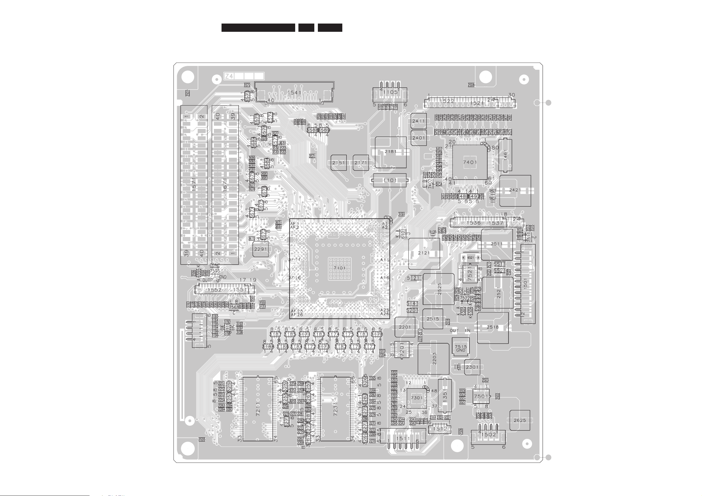
EN 36
3139 785 3220x
7.Circuit Diagrams and PWB Layouts
Layout: Digital-Main Part (Top View)
DVDR3455D_TopView.pdf 2006-05-25
Page 37
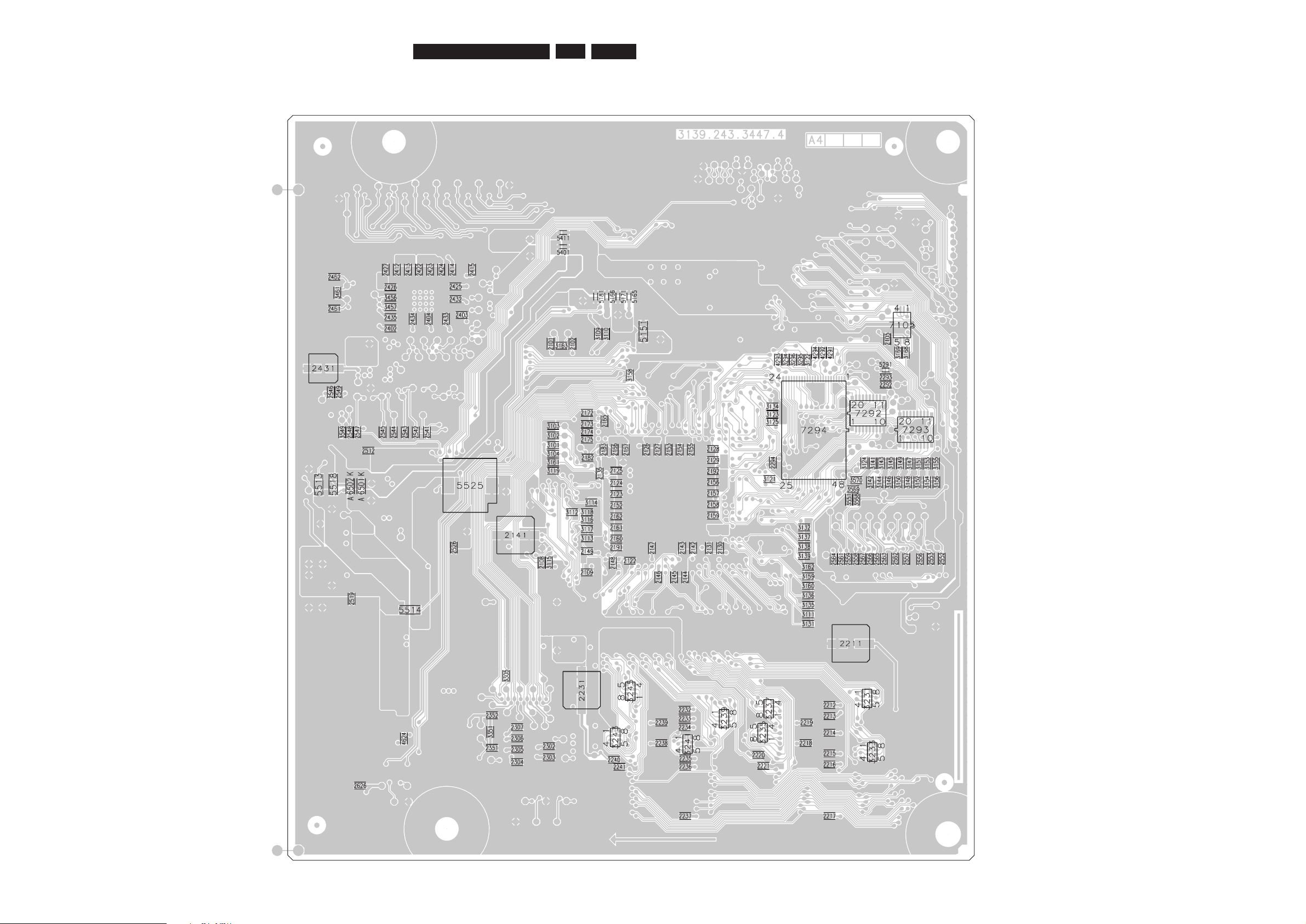
EN 37
3139 785 3220x
7.
Circuit Diagrams and PWB Layouts
Layout: Digital-Main Part (Bottom View)
DVDR3455D_BtmView.pdf 2006-05-25
Page 38
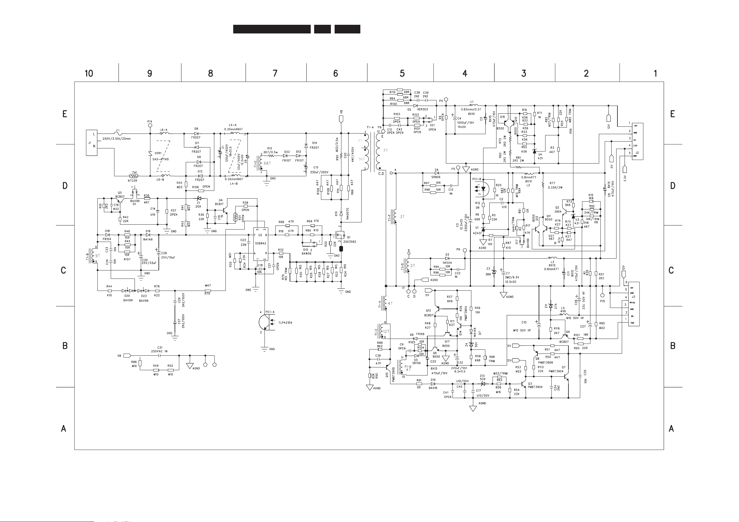
EN 38
3139 785 3220x
7.Circuit Diagrams and PWB Layouts
Power Supply Unit: Schematic
3139_247_12862.pdf 2006-05-31
Page 39

EN 39
3139 785 3220x
7.
Circuit Diagrams and PWB Layouts
Power Supply Unit: Layout
The PSU
Layout is not
available
Page 40

EN 40
3139 785 3220x
7.
Circuit Diagrams and PWB Layouts
Notes:
Page 41
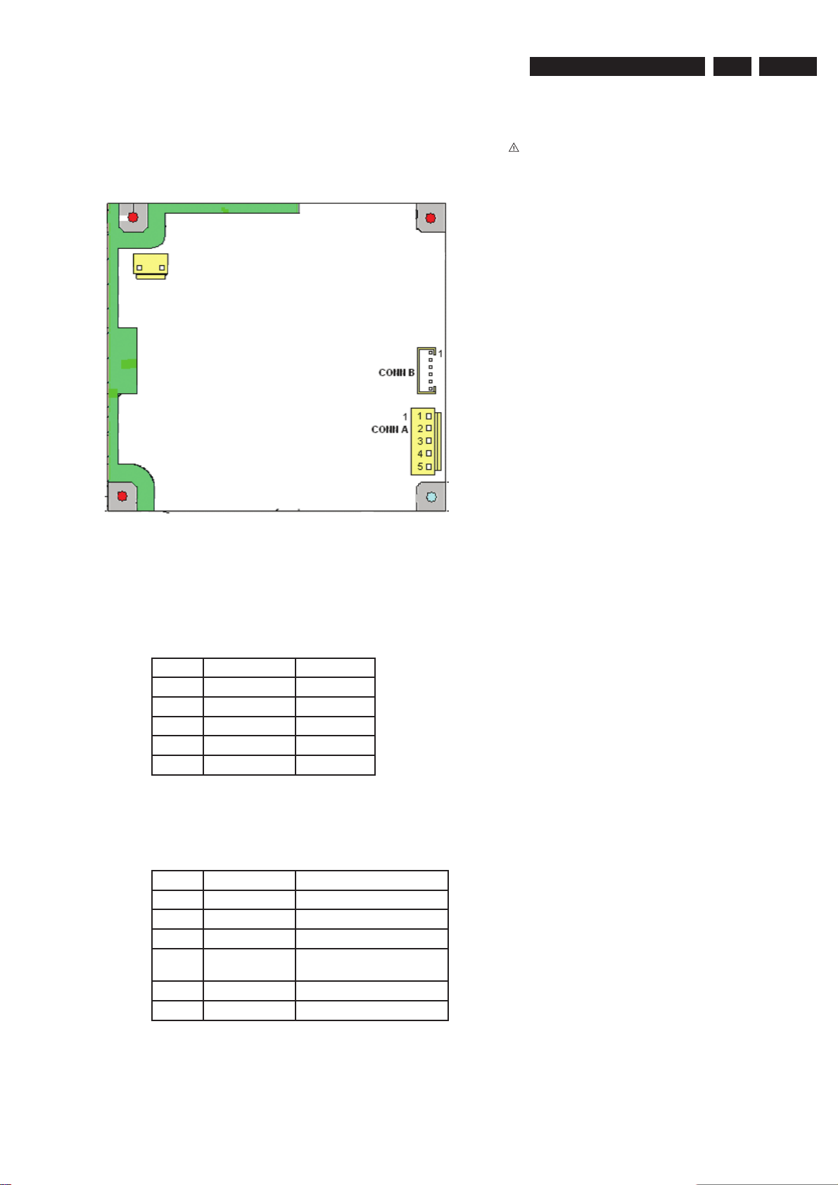
Circuit- and IC description
8. Circuit- and IC description
EN 413139 785 3220x 8.
8.1. PSU Board
8.1.1. General
Figure 8-1 PSU Board Layout
attempting the procedure mentioned below:
The Mains must be disconnected from the Set before
The PSU is designed with short-circuit protection that
will shutdown the power supply. When this happen,
the voltage stored in capacitor C1 and C40 will prevent
the Power Supply to turn-on, therefore they must be
discharged with a screwdriver with high electrical
isolation handle before the PSU can function normally
again.
Note: During the process of discharging the capacitors,
spark can be observed which is typical of the high
voltage stored in Capacitor C1 and C15.
The PSU board provides the following connection to the
rest of the set:
• Connector A: Supply/Signal to Analog Board
Conn. 1401
• Serve as supply to Digital Board
Pin no. Supply / Signal Remarks
112V
2 GND
35V
4 3.3V
5 GND
• Connector B: Supply/Signal to Analogue Board
Conn. 1402
• Serve as 12VBE to Digital Board,only supplied upon
triggered by STBYn lines from transistor 7421(Analog
Board)
Pin no. Supply / Signal Remarks
1VGN
25N
3 GND
4 IP_FAIL HIGH>4.0v = power good
5 GND
612V
LOW<4.0v =power fail
Page 42

EN 42 3139 785 3220x8.
Circuit- and IC Description
8.2. Front Board (Panel – Display + Key)
8.2.1. General
This board consists of the following parts:
• FIP Control Driver
• Frontend (Audio & Video)
• VFD Heater voltage Generator
8.2.2. FIP Control Driver (IC 7105: UPD16316GB)
The core element of the Front Display + Keyboard is
the FIP Control Driver. It runs on a 5V supply and is
responsible for the following functions:
• Interface with the Domino chip on the Digital Board
• Evaluation of the keyboard matrix within Front board
• Decoding the remote control commands from the
infra-red receiver
• Activation and control of the display
• Timer Wake-up activation
It runs on two clock frequencies namely:
• 5MHz for normal operation
• 32.768KHz for the real time clock
8.2.3. Interface to the Domino chip
It communicates with the Domino Host on the Digital
board via a 6-wire synchronous serial interface. The
Host is always the master to generate the communication
clock to the FIP Control Driver irrespective of the
direction of data transfer.
8.2.4. Evaluation of the keyboard matrix
8.3. Analog Board
8.3.1. General
The PCBA consist of the following parts:
• Fan Control
• Tuner Frontend
• Audio ADC/DAC
8.3.2. Tuner Frontend [1100 : TMQZ2]
The Analog board supports 2 possible Tuner Frontend
unit namely:
• 1101 – PAL BG,DK and I Broadcast System
• 1100 – NTSC-M Broadcast System
It has a RF IN for antenna connection and RF OUT which
provides a RF loop through for connection to the TV.
The Frontend ( Tuner & IF-demodulator ) is controlled
by I2C (SCL_5V- and SDA_5V-) lines coming from the
Domino Host on the Digital board.
Complete video processing is done in this unit and the
video output (CVBS) is taken out from the [VIDEO_OUT]
pin 13 via a transistor as CVBS_TV-line to the Video I/O
circuitry. The audio-IF component SIF1 is taken out from
the [SIF_OUT] pin 10 for the demodulation by the Multisound processor (MSP).
Audio demodulator
The sound demodulation is done by the MSP3425 [7304],
which is also fully controlled via I2C bus by the Domino
Host. The audio signals are available at pin 30 and pin 31
and fed as AIA_R_MSP & AIA_L_MSP line to the audio I/O
for further processing.
A key matrix is used on the Front board. The slave μP
does the key scanning with FIP9 - FIP24 (pin 23-26 and
29-40) as output and KEY_A - KEY_C (pin 41-43) as input.
Each key is assigned a key code based on the output
and input ports, and the FIP Control Driver will do the
evaluation by getting the key code.
8.2.5. IR receiver and signal evaluation
The IR receiver on the Front Board contains a selectively
controlled amplifi er as well as a photodiode. The photo-
diode changes the received infrared transmission
to electrical pulses, which are then amplifi ed and
demodulated. On the output of the IR receiver, a pulse
sequence with TTL-level, which corresponds to the
envelope curve of the received IF remote control
command can be measured. This pulse sequence is fed
into the FIP Control Driver for further processing via pin
13.
8.2.6. Vacuum Fluorescent Display [1203: HUV-08SS65T]
The VFD is fully controlled and driven by the FIP Control
Driver.
8.2.7. VFD Heater Voltage Generator
The oscillator circuit provided by [5100, 2101, 2102
& 7100] provides the necessary sine wave signal
transistors [7101, 7102 & 7103] to generate the 50% dutycycle 48KHz AC square-wave signal for the fi lament of
the VFD.
8.2.8. Timer Wake-up activation
During the Standby mode, the FIP Control Driver provides
a wakeup service (POWER_CTL-line switches to high),
then the Domino Host (on the Digital Board) starts up and
asks for the wake-up reason.
Page 43
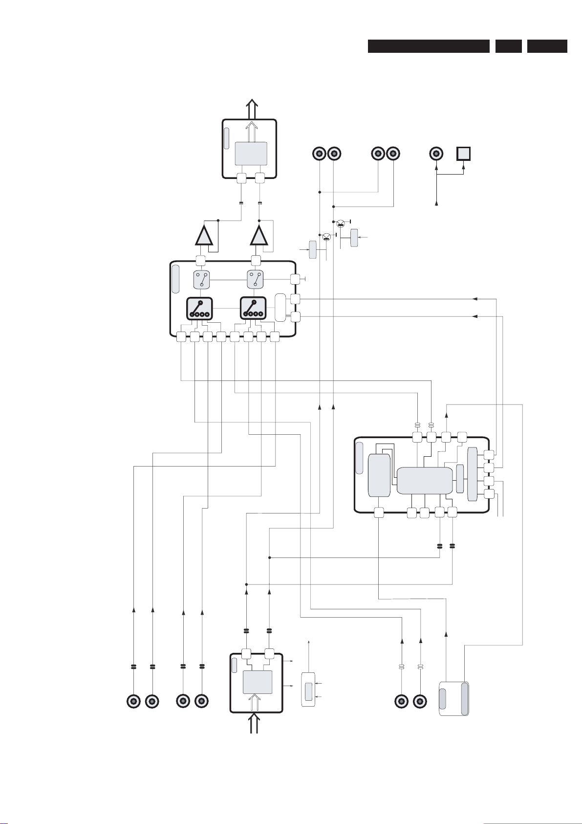
8.3.3. Audio routing
L
H
L
H
Circuit- and IC description
to FEBE /
digital board
A_DATA
POS:7203
UDA1361TS
ADC
3
1
ARADC
ALADC
REAR OUT2
AR
AOUTA
(CVBS / YC)
AL
AOUTB
REAR OUT1
(YUV)
AR
EN 433139 785 3220x 8.
AL
Dig.Audio Out
from digital
DA OUT
Optical Audio Out (OPTION)
board
Audio IO
0dB
3
POS:7201
HEF4052B
MSB/LSB
LH
LL
HL
3
5
AINFL
2
AIN1L
HHLHLL
5
4
AIN2L
1
1
1
AFEL
12
AFER
14
AINFR
0dB
13
HL
AIN1R
MUTE
AKILL
AMUTEC
MSP3415G
Demodulator
SIF1
RSA2
RSA1
AMCO
AIA_L_MSP
AIA_R_MSP
31
26
DACM_R
Source select
37
38
ALDAC
ARDAC
27
DACM_L
I2C Control
Q.Peak Det
9
8
13
12
SDA_5V
SCL_5V
30
SC1_OUT_L
SC1_OUT_R
2
41
40
MUTE
BMUTEC
6
109
Logic
MSB LSB
HH
11
15
AIN2R
AKILL
AIA_R_RE2
REAR IN-EXT2
(CVBS / YC)
AIA_L_RE2
AIA_R_RE1
REAR IN-EXT 1
(YUV)
AIA_L_RE1
CS4351
POS:7206
AOUTB
AOUTA
14
16
VOR
VOL
DAC
D_DATA
from FEBE /
digital board
AKILL
BMUTEC
AMUTEC
MUTE
Figure 8-2 Analog Audio IO
IPFAIL
DKILL
AINFR
AINFL
SIF1
Tuner
from CU
AMCO
Modulator
Page 44

EN 44 3139 785 3220x8.
The sound processing is always done in stereo (that
means separate left- and right- channel) and the complete
switching is realized by using HEF4052, which is a dual
four-to-one multiplexer and MSP3415G, multi-sound
processor.
a) Record path
The complete selection of audio signal for recording is
done by a HEF4052 [7201], which is a dual four-to-one
multiplexer. The input lines for the selector [7301] are
coming either from MSP [7304] (AIA_L_MSP/AIA_R_MSP)
or cinch rear-in Ext AIA_R_RE1/AIA_L_RE1) or the cinch
front-in (AIA_R_FR/AIA_L_FR). The [7201] controlled via
RSA1- and RSA2- signals coming from the MSP [7500].
The MSP acts as a port expander of the FIP Control
Driver. The Op-Amp on the output [7201] is necessary
for performance reasons and acts also as a driver. The
selected signals ALADC* and ARADC* are directly fed to
the Audio-ADC. As there is also a fi fth input (DV-in), the
corresponding audio signals (ALDAC*/ARDAC*) from the
Digital board are routed via the MSP [7304] and output as
AIA_R_FR/AIA_L_FR to selector [7201]
b) Cinch out
The Multiplexer (HEF7201) selects signals from a few
sources, namely Rear Cinch In (AIA_R_RE1/AIA_L_RE1),
Front Cinch In (AIA_R_FR/AIA_L_FR) and MSP (AIA_L_
MSP/AIA_R_MSP). The multiplexer is controlled via RSA1
and RSA2 signals coming from the MSP.
Circuit- and IC Description
c) Digital audio-out path
In addition to the analog output the set is also equipped
with a digital audio output via cinch plug [1131]. The
signal is generated on the digital board and routed
via the audio interface cable and connector [1600] to
the Analog board. Here the DAOUT-line fi rst passes
a 6-fold inverter [7700] being used as a driver and for
performance reasons (noise reduction, jitter,etc).
8.3.4. Audio ADC/DAC
The conversion of analog audio signals (ALADC*/
ARADC*) from the record-selector [7201] is done via
AID_DAT [7203]. This IC can process input signals up
to 2Vrms by using external resistors in series to the
input pins. All required clock signals are generated on
the digital board and only the audio data (AID_DAT)
are routed from the Analog to Digital board for further
processing.
The transformation of digital audio back into analog
domain is done by CS4351 [7206]. All necessary clock
signals are coming from the digital board and digital
audio data (D_DATA0-line) are converted into analog
signals (pin 15 and 18). The output signals from the
audio DAC part (AOUTA/AOUTB) are directly routed to
the rear cinch sockets. To avoid plops and any other
audible noise on the output there is a mute-stage
implemented for each channel. The activation of the mute
function is done via the AMUTEC & BMUTEC (digital
silence mute) from the audio DAC and also the AKILL line
which is a combination of the D_KILL from the Digital
board and POWER_FAIL from power supply.
*Note: ALADC refers to VINL of IC7203
ARADC refers to VINR of IC 7203
Page 45
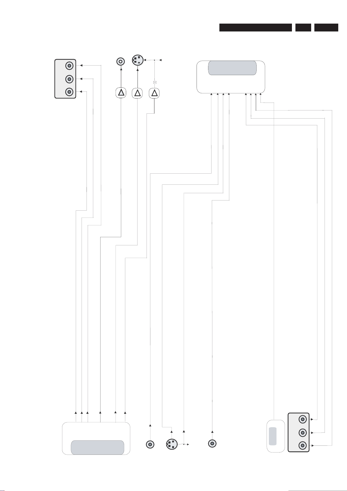
8.3.5. Video routing
V (Pr)
V (Pr)
U (Pb)
U (Pb)
REAR OUT
REAR OUT1
Y
Y
REAR OUT2
REAR OUT
Y/C
CVBSR_OUT
Circuit- and IC description
S-CONN
WSRO
CR_OUT
VY_OUT
Y_REAR
C_REAR
CVBS_REAR
CVBS_FIN
Y_FIN
To digital board
To digital board
C_FIN
A_V
A_U
A_Y
EN 453139 785 3220x 8.
CVBS_TV
Video IO
Video IO
VIA_RPr
VIA_BPb
VIA_GY
D_CVBS
VOA_SY
VOA_SC
From digital board
CVBS
CVBS_REAR
Y_REAR
Y/C
REAR IN -EXT2
C_REAR
WSRI
to CU
CVBS
FRONT IN
TUNER
V (Pr)
V (Pr)
U (Pb)
U (Pb)
REAR IN-1
REAR IN-EXT1
Y
Y
Figure 8-3 Analog Video IO
Page 46
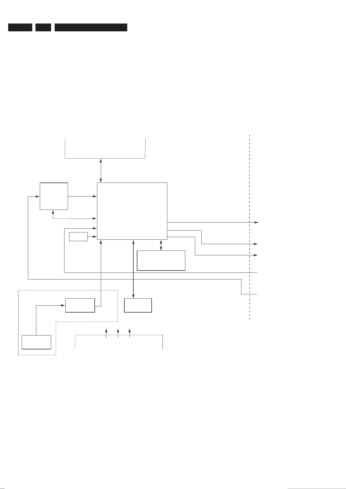
EN 46 3139 785 3220x8.
Circuit- and IC Description
The switching of the various video input signals is done
by the Video Input Processor on the Digital Board. These
signals are directly routed to the digital board through
connector 1122 on the Analog Board
8.4. Digital Board
The Digital Board is based on the highly integrated LSI
‘Domino’ BGA chip (Ball Grid Array), DMN-8652. This IC
has 2 on-chip ATAPI controller and integrates an analog
8.4.1. Record Mode
TO/FROM FRONTEND PART
ATAPI
7401
7101
VIP
TVP5146
ITU656
I2C
CLOCK
13.5MHz
DMN 8652
7211/7231
DDR SDRAM
16M X 16Bit
video encorder, and provides build-in support for nonsimultaneous progressive and interlaced video output.
A 1394 link layer function is also integrated, requiring
only a simple external physical layer device. The board
encodes and multiplexes analogue video and digital
uncompressed audio (I2S) into an MPEG2 stream. This
MPEG2 stream is formatted for recording by the DVD+RW
engine. In the playback, the board will decode the MPEG2
video into analogue video. In addition, a DV stream can
be received via IEEE 1394 (i-Link), and transformed to
MPEG2 format.
1FH VIDEO
(2)
OUT
DIG. AUDIO OUT
2
I
S A UDIO OUT
2
S A UDIO IN
I
For DV-in version only
1512
1394
CONNECTOR
7304
1394
TSB41AB1
FLASH
16M Bit
5V 12V3V3
FROM POWER SUPPLY
Figure 8-4 Domino block
7294
(1) analogue CVBS / YC and RGB/YUV
(2) analogue CVBS, YC, RGB/YUV
1FH VIDEO IN
(1)
Page 47
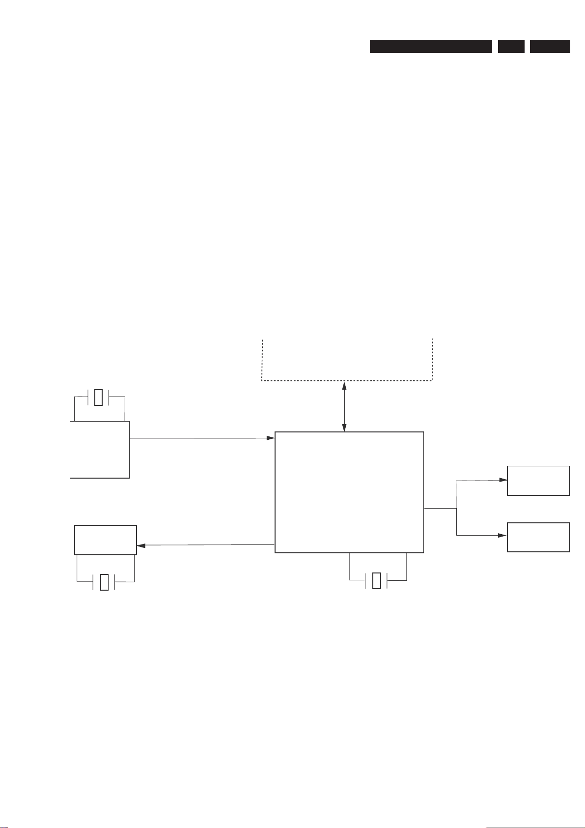
Circuit- and IC description
EN 473139 785 3220x 8.
Video Part
The digital video input signals from the DV-in on the
Front board are routed from connector 1521 via the IEEE
1394 PHY IC [7301] to the Domino chip [7101].
The Video Input Processor encodes the analogue video
to digital video stream (CCIR656 format). The output
stream, named VID_D (0:9), is then routed to the Domino
chip. This IC encodes and decodes the digital video
stream into / from MPEG2 format.
Audio Part
2
S audio is sent from the Analog board to the Domino
I
chip via connector 1536.
The Domino chip compresses the I2S audio data into an
MPEG1-L2 / AC3 audio stream.
8.4.4. Clock Distribution
2
Front-end I
The Domino chip interfaces directly to the basic Engine
via ATAPI connector 1571.
It buffers the data streams that are coming from (or going
to) the Basic Engine.
In the Domino chip, the video MPEG2 stream and the
audio AC3 stream are sent to the basic Engine for
recording through ATAPI bus.
8.4.2. Playback mode
During playback, the data from the Basic Engine is going
directly to the Domino chip via ATAPI interface. The
Domino chip has the following outputs:
• Analogue video CVBS, YC and RGB outputs on
connector 1521
• I
• SPDIF audio (digital audio output) on connector 1536
8.4.3. Basic Engine Interface
The Digital board is equipped with an IDE bus (ATAPI) for
connecting to the Basic Engine.
S
2
S audio (PCM format) on connector 1536
14.31818MHz
7401
VIP
TVP5146
7301
1934 PHY
24.576 MHz
FRONTEND INTERFACE
7101
DMN 8652
13.5 MHz
Figure 8-5 DIMINO_CLOCK
7211
150 MHz
SDRAM
7231
SDRAM
The Domino chip has a complex system, which is needed
to support the processes running at different frequencies
such as video decoding, audio decoding or peripheral
I/O devices etc. To ensure a synchronous initialization
of all the registers and state machines, all the PLLs are
switched to their default frequency 27MHz.
Then when the booting control unit is correctly initialized
and once it has captured all the booting parameters, it
sets the PLLs to its functional frequencies. Thanks to a
clock blocking mechanism, the frequency switching is
glitch free.
System clocks:
• DMN-8652 (7101, pin A1 and A2) : 13.5 MHz provided
by the x’tal 1101
• DMN-8652 1394-LINK (7101, pin K1) : 49.152MHz
provided by 1394-PHY
• TVP5146 (7401, pin 74 and 75) : 14.31818MHz
provided by x’tal 1461
• SDRAM (7211 and 7231, pin 45 and 46) : 150MHz
provided by the DMN-8652
• TSB41AB1PHP IEEE 1394 PHY IC (7301, pin 42 and
43) : 24.576MHz provided by x’tal 1351
Page 48
EN 48 3139 785 3220x8.
8.4.5. Power Supply
Circuit- and IC Description
The Digital board is not powered in standby mode. The
control signal STBY on the analog board will enable the
PSU and power the digital board.
• STBY = Low: the digital board is in powered down
standby mode
• STBY = High: the power supply to the digital board is
enabled.
The 3V3, +5V and +12V come from the PSU, while the
following voltages are generated in the digital board:
• 1.8V core voltage is generated on the board by a 2A
switching step down voltage regulator [7521]
8.4.7. Reset
5V Supply
HOSTRST
MICROPROCESSOR
SYSRST#
FRONT
• 2.5V supply for the SDRAM is generated by an ultra
fast low dropout linear regulator [7515]
• 1.25V DDR termination supply is generated by
regulator [7201]
8.4.6. Memory
• FLASH IC7294: this memory contains the boot
parameters and application fi rmware
IDE_RST#_1
DMN 8652
1
Delay t
Basic Engine
VAD8041
2
Delay t
POWER ON
RESET & LOW
VOLTAGE
DETECTION
NCP303LSN30
IC7595
RSTn
Reset concept Digital board
The rest circuitry [7595] takes cares that the different
devices on the digital board are boot-up in the correct
order. At power on the reset circuitry provides the
following resets (delay τ1):
• SYS_RST# to the Domino chip [7101] and Flash
Memory [7294]
The Domino chip then generates other reset signals
(delay τ2) via its GPIOs:
• VID_RST# to reset the VIP [7401]
• LNK_RST# to reset the IEEE1394 DV PHY IC [7301]
• IDE_RST#_1 to reset Basic Engine
FLASH MEMORY
1
Delay t
Figure 8-6 DOMINO_RESET
8.4.8. I/O Connector
Audio IO Connector (item 1536)
The Audio In/Out (AIO) connector is used to interchange
digital audio signals between the Analog and Digital
board
Video IO Connector (item 1521)
The Video In/Out (VIO) Connector is used to interchange
analogue video signals between the Analog and Digital
board
VID_RST#
VIP_RST#
LNK_RST#
VIP (TVP5146)
2
Delay t
PDI1394P25BD
2
Delay t
Page 49
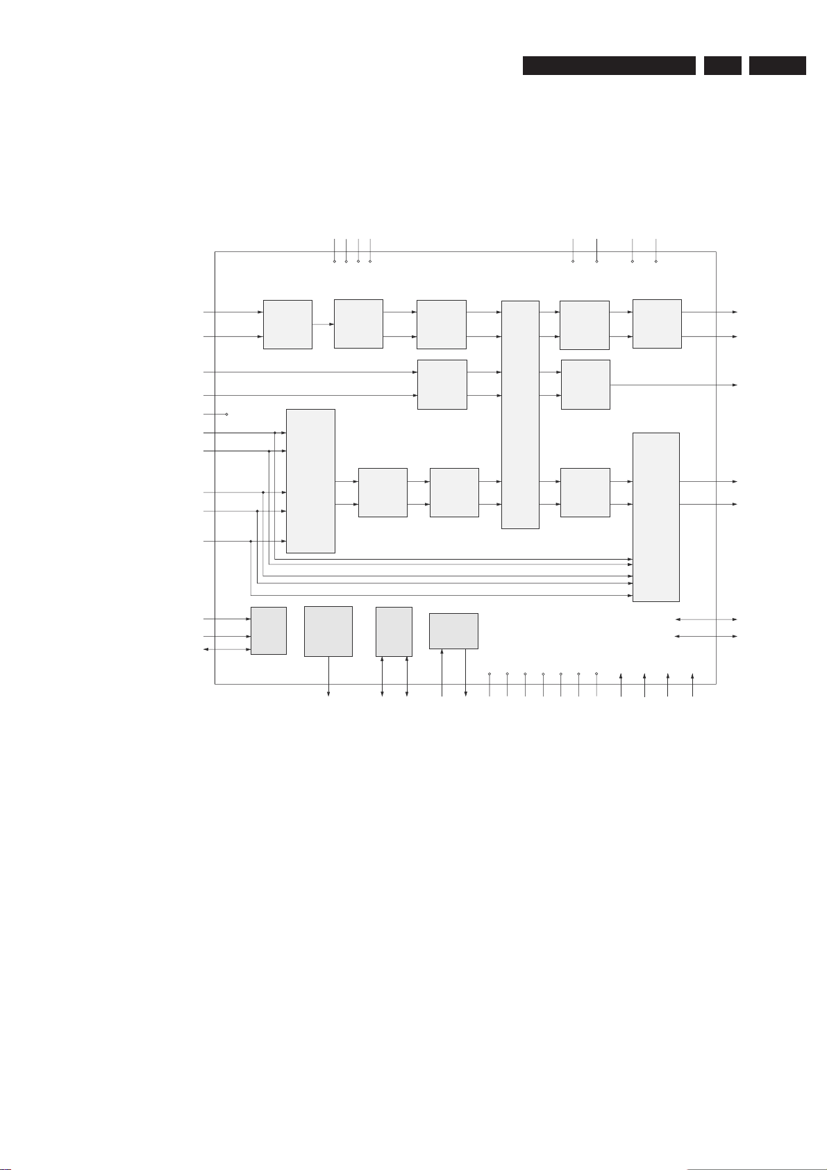
Circuit- and IC description
8.5 IC Description
8.5.1 Analog Board
IC7304 - Multistand Sound Processor Family
BLOCK DIAGRAM
EN 493139 785 3220x 8.
MSP34x5G
ANA_IN+
2
ANA_IN-
3
I2S_DA_IN1
17
I2S_DA_IN2
21
39
ASG
SC1_IN_L
40
SC1_IN_R
41
37
SC2_IN_L
SC2_IN_R
38
43
MONO_IN
10
ADR_SEL
I2C_CL
12
13
I2C_DA
2
I
C
Control
ADC
SCART
DSP
input
select
ADR BUS
23
24
N.C.
N.C.
De-
Modulator
DVSUP
DAC
SCART
Output
select
34
CAPL_M
DACM_L
DACM_R
I2S_DA_OUT
SC1_OUT_L
SC1_OUT_R
D_CTR_I/O-0
D_CTR_I/O-1
27
26
16
31
30
9
8
28
32
N.C.
N.C.
Pre-
processing
Pre-
processing
Source
select
ADC
2
I
S
Control
Prescale
X'tal
Oscillator
1
33 19
AVSUP
AHVSUP
Loud-
speaker
sound
proeessing
Loud-
speaker
sound
proeessing
DAC
ADR_CL
18
14
I2S_CL
I2S_WS
15
Figure 8-8
5
XTAL_IN
XTAL_OUT
6
AVSS
AHVSS
AGNDC
DVSS
VREF2
VREF1
36
35
44
25
20
29
RESETQ
VREFTOP
42
22
STANDBYQ
11
TESTEN
4
TP
7
Page 50
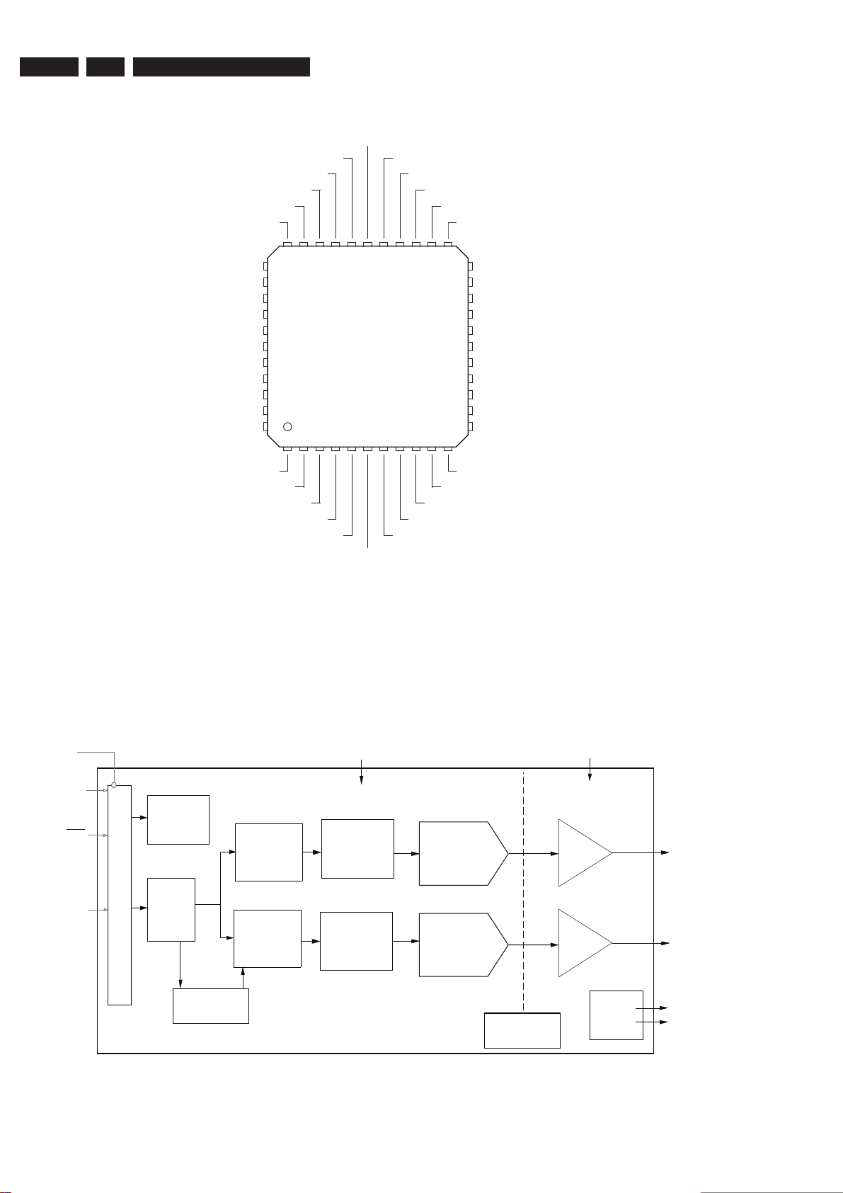
EN 50 3139 785 3220x8.
PIN CONFIGURATION
SC1_OUT_L
AHVSUP
SC1_OUT_R
NC
Circuit- and IC Description
NC
VREF1
DACM_L
DACM_R
VREF2
NC
NC
CAPL_M
AHVSS
AGNDC
SC2_IN_L
SC2_IN_R
ASG
SC1_IN_L
SC1_IN_R
VREFTOP
MONO_IN
AVSS
AVSUP
33 32 31 30 29 28 27 26 25 24 23
34
35
36
37
38
39
40
41
42
43
44
ANA_IN1+
ANA_IN−
MSP 34x5G
1234567891011
TESTEN
XTAL_IN
XTAL_OUT
PMQFP44 package
Figure 8-9
D_CTR_I/O1
TP
22
21
20
19
18
17
16
15
14
13
12
STANDBYQ
ADR_SEL
D_CTR_I/O0
RESETQ
I2S_DA_IN2
DVSS
DVSUP
ADR_CL
I2S_DA_IN1
I2S_DA_OUT
I2S_WS
I2S_CL
I2C_DA
I2C_CL
IC7206 - 192KHz Stereo DAC with 2vrms line-out
BLOCK DIAGRAM
1.8 V to 3.3V
Hard ware or I2C/SPI
Control Data
Register/Hardware
Reset
Serial Audio Input
Configuration
Interpo latio n
Filter with
Volume Control
PCM
Serial
Interface
Level Translator
Auto Speed Mode
Detect
Interpo latio n
Filter with
Volume Control
3.3 V
Multibit
ΔΣ Modulator
Multibit
ΔΣ Modulator
Figure 8-10
DAC
DAC
Internal Voltage
Reference
9 V to 12 V
Amp
+
Filter
Amp
+
Filter
External
Mute
Control
2 Vrms Line Level
Left Channel O utput
2 Vrms Line Level
Right Channel
Output
Left and Righ t
Mute Controls
Page 51
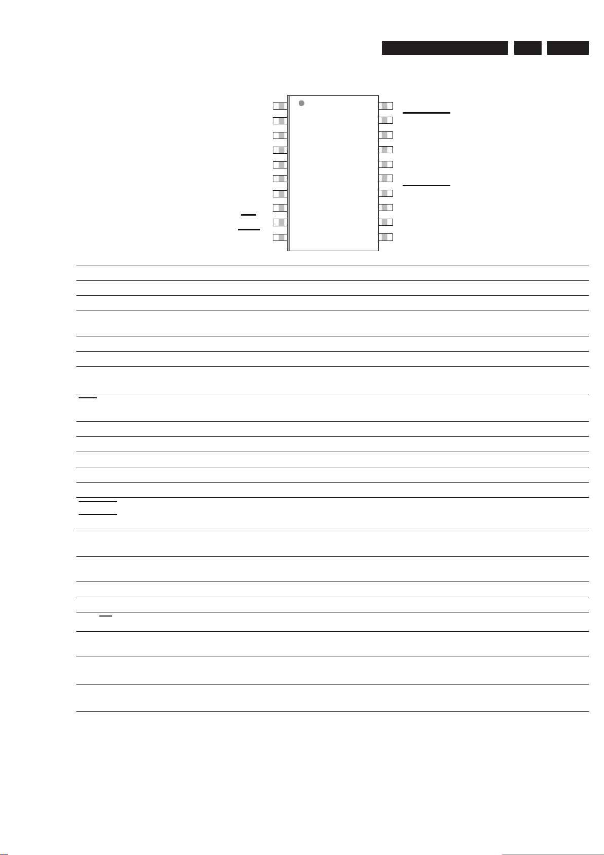
Circuit- and IC description
PIN DESCRIPTION AND CONFIGURATION
EN 513139 785 3220x 8.
SCLK AMUTEC
LRCK AOUTA
MCLK VA_H
DIF1(SCL/CCLK) BMUTEC
DIF0(SDA/CDIN) VQ
DEM(AD0/CS
Pin Name # Pin Description
SDIN
SCLK
LRCK
MCLK
VD
GND
RST
VA
VBIAS
VQ
VA_H
VL
BMUTEC
AMUTEC
AOUTB
AOUTA
Control Port
Definitions
SCL/CCLK
SDA/CDIN
Serial Audio Data Input (
1
Serial Clock (
2
Left / Right Clock (
3
audio data line.
Master Clock (
4
5 Digital Power (
Ground (
6
Input
Input
Input
Input
) - Ground reference.
16
Reset (
Input
10
enabled.
) - Powers down device and resets all internal resisters to their default settings when
11 Low Voltage Analog Power (
Positive Voltage Reference (
12
13 Quiescent Voltage (
17 High Voltage Analog Power (
Serial Audio Interface Power (
20
Mute Control (
14
Output
19
Analog Outputs (
15
tics
18
7
8
table.
Serial Control Port Clock (
Serial Control Data (
SDIN VL
VD GND
GND AOUTB
) VBIAS
RST
) - Serial clock for the serial audio interface.
Input
) - Clock source for the delta-sigma modulator and digital filters.
) - Positive power supply for the digital section.
Output
) - Control signal for optional mute circuit.
Output
Input/Output
1
2
3
4
5
6
7
8
9
10
Input
) - Input for two’s complement serial audio data.
) - Determines which channel, Left or Right, is currently active on the serial
Input
) - Positive power supply for the analog section.
Output
) - Positive reference voltage for the internal DAC.
) - Filter connection for internal quiescent voltage.
Input
) - Positive power supply for the analog section.
Input
) - Positive power for the serial audio interface
) - The full scale analog line output level is specified in the
Input
) - Serial clock for the control port interface.
) - Input/Output for I2C data. Input for SPI data.
20
19
18
17
16
15
14
13
12
11
VA
Analog Characteris-
AD0/CS
Stand-Alone
Definitions
DIF0
DIF1
DEM
Address Bit 0 / Chip Select (
9
Digital Interface Format (
8
Clock, and Serial Audio Data.
7
De-emphasis (
9
sample rates
Input
Input
) - Chip address bit in I2C Mode. Control Port enable in SPI mode.
Input
) - Defines the required relationship between the Left Right Clock, Serial
) - Selects the standard 15μs/50μs digital de-emphasis filter response for 44.1 kHz
Page 52
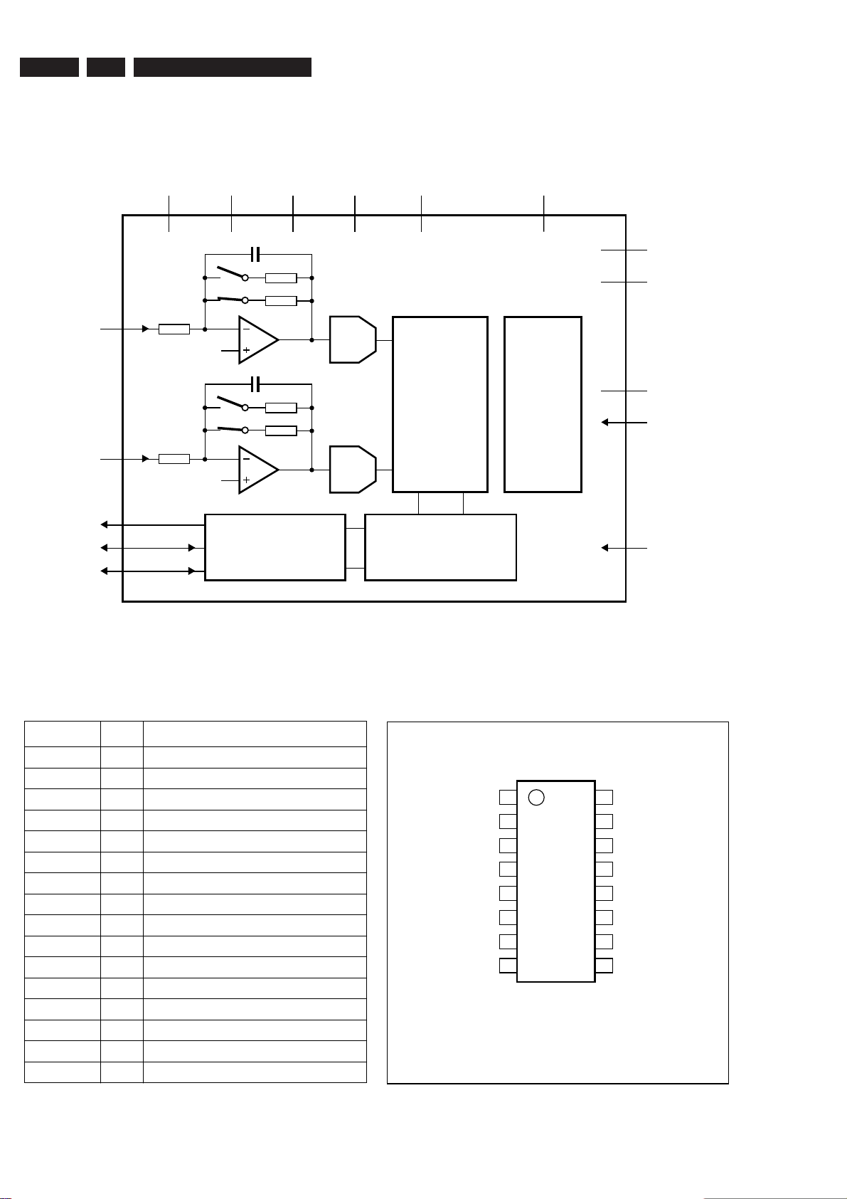
EN 52 3139 785 3220x8.
IC7203 - 96KHz Sampling 24-bit stereo audio ADC
BLOCK DIAGRAM
Circuit- and IC Description
th
V
INL
V
INR
DATAO
BCK
WS
1
3
13
11
12
V
DDA
16
V
SSA
15
DIGITAL
INTERFACE
V
RP
5
V
RN
4
V
ref
2
UDA1361TS
SYSCLK
8
10
9
V
DDD
V
SSD
ADC
ΣΔ
ADC
DECIMATION
FILTER
14
CLOCK
CONTROL
MSSEL
7
PWON
ΣΔ
DC-CANCELLATION
FILTER
6
SFOR
PIN DESCRIPTION AND CONFIGURATION
SYMBOL PIN DESCRIPTION
V
INL
V
ref
V
INR
V
RN
V
RP
1 left channel input
2 reference voltage
3 right channel input
4 negative reference voltage
5 positive reference voltage
SFOR 6 data format selection input
PWON 7 power control input
SYSCLK 8 system clock 256, 384, 512 or 768f
V
V
DDD
SSD
9 digital supply voltage
10 digital ground
BCK 11 bit clock input/output
WS 12 word select input/output
DATAO 13 data output
MSSEL 14 master/slave select
V
V
SSA
DDA
15 analog ground
16 analog supply voltage
Figure 8-11
handbook, halfpage
s
V
INL
V
ref
V
INR
V
RN
V
RP
SFOR
PWON
SYSCLK
1
2
3
4
UDA1361TS
5
6
7
8
MGT452
MGT451
16
15
14
13
12
11
10
9
V
DDA
V
SSA
MSSEL
DATAO
WS
BCK
V
SSD
V
DDD
Page 53
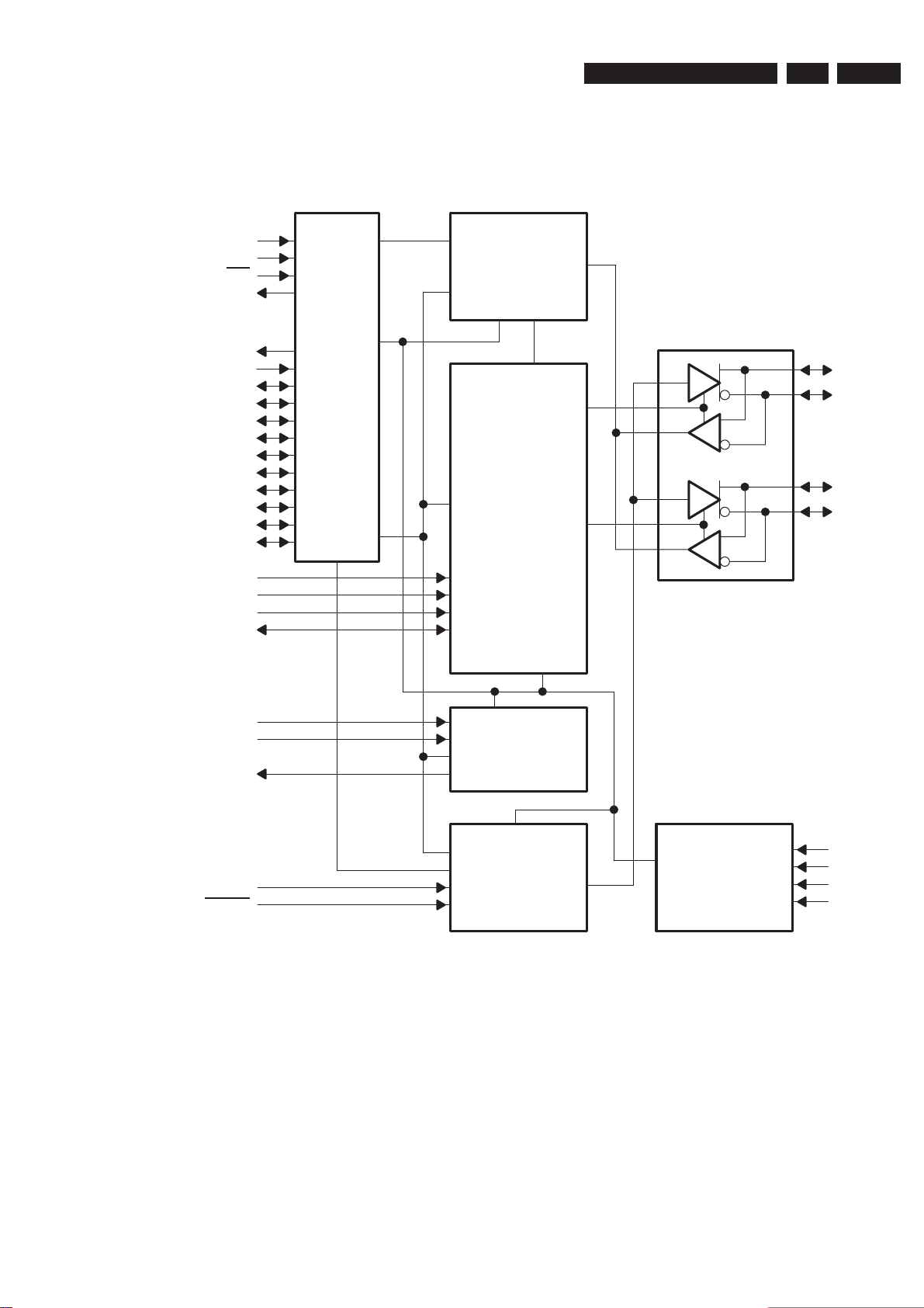
Circuit- and IC description
8.5.2 Digital Board
IC7301 - IEEE 1394a-2000 one port cable Transceiver/Arbiter
BLOCK DIAGRAM
EN 533139 785 3220x 8.
CPS
LPS
ISO
CNA
SYSCLK
LREQ
CTL0
CTL1
D0
D1
D2
D3
D4
D5
D6
D7
PC0
PC1
PC2
C/LKON
Received Data
†
Link
Interface
I/O
Decoder/Retimer
Arbitration
and Control
State Machine
Logic
TPA+
TPA–
Cable Port
TPB+
TPB–
R0
R1
TPBIAS
PD
RESET
†
CNA output is only available in the 64-pin PAP package
Bias Voltage
and
Current
Generator
Transmit Data
Encoder
Figure 8-12
Crystal
Oscillator,
PLL System,
and Clock
Generator
XI
XO
FILTER0
FILTER1
Page 54
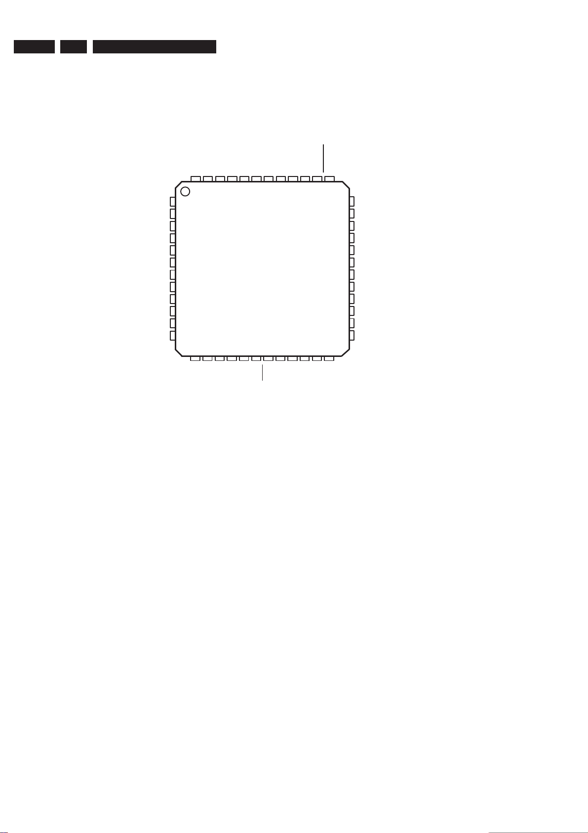
EN 54 3139 785 3220x8.
PIN CONFIGURATION
PHP package terminal diagram
Circuit- and IC Description
PHP PACKAGE
(TOP VIEW)
SYSCLK
CTL0
CTL1
D0
D1
D2
D3
D4
D5
D6
D7
PD
LREQ
DGND
DGND
47 46 45 44 4348 42 40 39 3841
1
2
3
4
5
6
7
8
9
10
11
12
14 15
13
16
LPS
DGND
C/LKON
DDDVDD
XO
DV
XI
TSB41AB1
17 18 19 20
PC0
ISO
PC1
PC2
Figure 8-13
DD
PLLGND
PLLV
FILTER1
22 23 24
21
DD
CPS
DV
TESTM
RESET
FILTER0
37
SE
SM
36
35
34
33
32
31
30
29
28
27
26
25
AGND
AV
DD
R1
R0
AGND
TPBIAS
TPA+
TPA–
TPB+
TPB–
AGND
AV
DD
Page 55
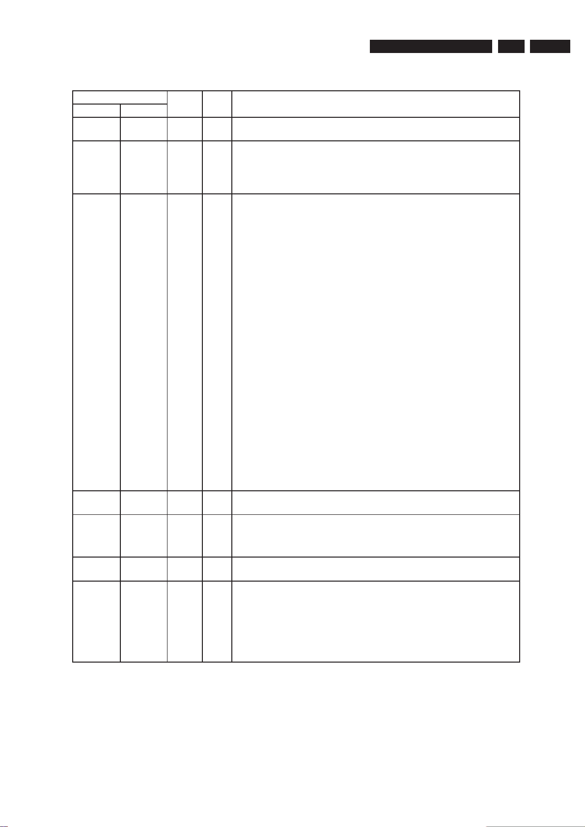
PIN DESCRIPTION
Circuit- and IC description
EN 553139 785 3220x 8.
TERMINAL
NAME
AGND
AV
DD
C/LKON
CNA
CPS
CTL0
CTL1
D0
D1
D2
D3
D4
D5
D6
D7
PHP NO.
26, 32, 36 Supply – Analog circuit ground terminals. These terminals should be tied together to the
25, 35 Supply – Analog circuit power terminals. A combination of high frequency decoupling
15 CMOS I/O Bus manager contender programming input and link-on output. On hardware reset,
N/A CMOS O Cable-not-active output. This terminal is asserted high when there is no incoming
20 CMOS I Cable power status input. This terminal is normally connected to cable power
2
3
4
5
6
7
8
9
10
11
TYPE I/O DESCRIPTION
low-impedance circuit board ground plane.
capacitors near each terminal is suggested, such as paralleled 0.1 μF and 0.001
μF. Lower frequency 10 μF filtering capacitors are also recommended. These
supply terminals are separated from PLLVDD and DVDD inside the device to provide
noise isolation. They should be tied at a low-impedance point on the circuit board.
this terminal is used to set the default value of the contender status indicated during
self-ID. Programming is done by tying the terminal through a 10-kΩ resistor to a high
(contender) or low (not contender). The resistor allows the link-on output to override
the input. However, it is recommended that this terminal should be programmed
low, and that the contender status be set via the C register bit.
If the TSB41AB1 is used with an LLC that has a dedicated terminal for monitoring
LKON and also setting the contender status, then a 1-kΩ series resistor should be
placed on the LKON line between the PHY and LLC to prevent bus contention.
Following hardware reset, this terminal is the link-on output, which is used to notify
the LLC to power up and become active. The link-on output is a square-wave signal
with a period of approximately 163 ns (8 SYSCLK cycles) when active. The link-on
output is otherwise driven low, except during hardware reset when it is
high-impedance.
The link-on output is activated if the LLC is inactive (LPS inactive or the LCtrl bit
cleared) and when:
a) the PHY receives a link-on PHY packet addressed to this node, or
b) the PEI (port-event interrupt) register bit is 1, or
c) any of the CTOI (configuration-time-out interrupt), CPSI
(cable-power-status interrupt), or STOI (state-time-out
interrupt) register bits are 1 and the RPIE (resuming-port
Once activated, the link-on output continues active until the LLC becomes active
(both LPS active and the LCtrl bit set). The PHY also deasserts the link-on output
when a bus reset occurs unless the link-on output would otherwise be active
because one of the interrupt bits is set (that is, the link-on output is active due solely
to the reception of a link-on PHY packet).
NOTE: If an interrupt condition exists which would otherwise cause the link-on
output to be activated if the LLC were inactive, the link-on output is activated when
the LLC subsequently becomes inactive.
bias voltage.
through a 400-kΩ resistor. This circuit drives an internal comparator that is used to
detect the presence of cable power. This terminal should be tied directly to DV
supply if application does not require it to be used.
CMOS I/O Control I/Os. These bidirectional signals control communication between the
TSB41AB1 and the LLC. Bus holders are built into these terminals.
CMOS I/O Data I/Os. These are bidirectional data signals between the TSB41AB1 and the
LLC. Bus holders are built into these terminals.
interrupt enable) register bit is also 1.
DD
Page 56
EN 56 3139 785 3220x8.
Circuit- and IC Description
TERMINAL
NAME
DGND
DV
DD
FILTER0
FILTER1
ISO
LPS
LREQ
PC0
PC1
PC2
PD 12 CMOS I Power-down input. A high on this terminal turns off all internal circuitry except the
PHP NO.
14, 46, 47 Supply – Digital circuit ground terminals. These terminals should be tied together to the
21, 44, 45 Supply – Digital circuit power terminals. A combination of high-frequency decoupling
38
39
19 CMOS I Link interface isolation control input. This terminal controls the operation of output
13 CMOS I Link power status input. This terminal monitors the active/power status of the link
48 CMOS I LLC request input. The LLC uses this input to initiate a service request to the
16
17
18
TYPE I/O DESCRIPTION
low-impedance circuit board ground plane.
capacitors near each terminal is suggested, such as paralleled 0.1 μF and
0.001 μF. Lower frequency 10 μF filtering capacitors are also recommended.
These supply terminals are separated from PLLVDD and AVDD inside the device to
provide noise isolation. They should be tied at a low-impedance point on the circuit
board.
CMOS I/O PLL filter terminals. These terminals are connected to an external capacitor to form
CMOS I Power class programming inputs. On hardware reset, these inputs set the default
a lag-lead filter required for stable operation of the internal frequency multiplier PLL
running from the crystal oscillator. A 0.1 μF ±10% capacitor is the only external
component required to complete this filter.
differentiation logic on the CTL and D terminals. If an optional Annex J type isolation
barrier is implemented between the TSB41AB1 and LLC, the ISO terminal should
be tied low to enable the differentiation logic. If no isolation barrier is implemented
(direct connection), or TI bus holder isolation is implemented, the ISO
should be tied high to disable the differentiation logic. For additional information
refer to TI application note
SLLA011.
layer controller and controls the state of the PHY-LLC interface. This terminal
should be connected through a 10-kΩ resistor either to the VDD supplying the LLC,
or to a pulsed output which is active when the LLC is powered (see Figure 9). A
pulsed signal should be used when an isolation barrier exists between the LLC and
PHY. (See Figure 10.)
The LPS input is considered inactive if it is sampled low by the PHY for more than
2.6 μs (128 SYSCLK cycles), and is considered active otherwise (that is, asserted
steady high or an oscillating signal with a low time less than 2.6 μs). The LPS input
must be high for at least 21 ns to guarantee that a high is observed by the PHY.
When the TSB41AB1 detects that LPS is inactive, it places the PHY-LLC interface
into a low-power reset state. In the reset state, the CTL and D outputs are held in
the logic zero state and the LREQ input is ignored; however, the SYSCLK output
remains active. If the LPS input remains low for more than 26 μs (1280 SYSCLK
cycles), the PHY-LLC interface is put into a low-power disabled state in which the
SYSCLK output is also held inactive. The PHY-LLC interface is placed into the
disabled state upon hardware reset.
The LLC is considered active only if both the LPS input is active and the LCtrl
register bit is set to 1, and is considered inactive if either the LPS input is inactive
or the LCtrl register bit is cleared to 0.
TSB41AB1. Bus holder is built into this terminal.
value of the power class indicated during self-ID. Programming is done by tying
these terminals high or low. Refer to Table 9 for encoding.
cable-active monitor circuits, which control the CNA output (64-terminal PAP
package only). Asserting the PD input high also activates an internal pulldown on
the RESET terminal to force a reset of the internal control logic. (PD is provided for
legacy compatibility and is not recommended for power management in place of
IEEE 1394a-2000 suspend/resume LPS and C/LKON features.)
Galvanic Isolation of the IEEE 1394-1995 Serial Bus
terminal
,
Page 57
Circuit- and IC description
EN 573139 785 3220x 8.
TERMINAL
NAME
PLLGND
PLLV
DD
R0
R1
RESET
SE
SM
SYSCLK
TESTM
TPA+
TPA–
TPB+
TPB–
TPBIAS
XI
XO
PHP NO.
41 Supply – PLL circuit ground terminals. These terminals should be tied together to the
40 Supply – PLL circuit power terminals. A combination of high-frequency decoupling
33
34
37 CMOS I Logic reset input. Asserting this terminal low resets the internal logic. An internal
23 CMOS I Test control input. This input is used in manufacturing test of the TSB41AB1. For
24 CMOS I Test control input. This input is used in manufacturing test of the TSB41AB1. For
1 CMOS O System clock output. Provides a 49.152-MHz clock signal, synchronized with data
22 CMOS I Test control input. This input is used in manufacturing test of the TSB41AB1. For
30 Cable I/O
29 Cable I/O
28 Cable I/O
27 Cable I/O
31 Cable I/O Twisted-pair bias output. This provides the 1.86 V nominal bias voltage needed for
42
43
TYPE I/O DESCRIPTION
low-impedance circuit board ground plane.
capacitors near each terminal is suggested, such as paralleled 0.1 μF and 0.001
μF. Lower frequency 10 μF filtering capacitors are also recommended. This supply
terminal is separated from DVDD and AVDD inside the device to provide noise
isolation. It should be tied at a low-impedance point on the circuit board.
Bias – Current setting resistor terminals. These terminals are connected through an
Crystal – Crystal oscillator inputs. These terminals connect to a 24.576-MHz parallel
external resistor to set the internal operating currents and cable driver output
currents. A resistance of 6.34 kΩ ±1.0% is required to meet the IEEE Std
1394-1995 output voltage limits.
pullup resistor to VDD is provided so only an external delay capacitor is required for
proper power-up operation (see
section). The RESET terminal also incorporates an internal pulldown which is
activated when the PD input is asserted high. This input is otherwise a standard
logic input, and may also be driven by an open-drain type driver.
normal use this terminal may be tied to GND through a 1-kΩ pulldown resistor or
it may be tied to GND directly.
normal use this terminal should be tied to GND.
transfers, to the LLC.
normal use this terminal should be tied to VDD.
Twisted-pair cable A differential signal terminals. Board traces from the pair of
p
positive and negative differential signal terminals should be kept matched and as
short as possible to the external load resistors and to the cable connector.
Twisted-pair cable B differential signal terminals. Board traces from the pair of
p
positive and negative differential signal terminals should be kept matched and as
short as possible to the external load resistors and to the cable connector.
proper operation of the twisted-pair cable drivers and receivers, and for signaling
to the remote nodes that there is an active cable connection.
resonant fundamental mode crystal. The optimum values for the external shunt
capacitors are dependent on the specifications of the crystal used (see
selection
used, XI should be the input and XO should be left open, and the clock must be
supplied before the device is powered on.
in the Application Information section). When an external clock source is
power-up reset
in the Application Information
p
p
crystal
Page 58
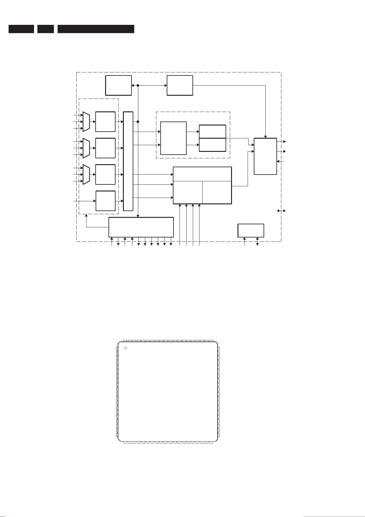
EN 58 3139 785 3220x8.
Circuit- and IC Description
IC7401 - 4x10bit DigitalVideo Decoder with microvision
BLOCK DIAGRAM
CVBS/
Pb/B/C
CVBS/
Y/G
CVBS/
Pr/R/C
CVBS/Y
VI_1_A
VI_1_B
VI_1_C
VI_2_A
VI_2_B
VI_2_C
VI_3_A
VI_3_B
VI_3_C
VI_4_A
Protection
Detector
Analog Front End
ADC1
ADC2
ADC3
ADC4
Sampling
Clock
Copy
M
U
X
Timing Processor
with Sync Detector
XTAL1
XTAL2
PWDN
RESETB
CVBS/Y/G
CVBS/Y
C
Y/G
Pb/B
Pr/R
AVID
DATACLK
VBI
Data
Slicer
Composite and S-Video Processor
Y/C
Separation
5-line
Adaptive
Comb
Y
C
Luma
Processing
Chroma
Processing
Component
Processor
Gain/Offset
Conversion
FID
GLCO
HS/CS
DRDGDB
FSO
VS/VBLK
Color
Space
YCbCr
YCbCr
Host
Interface
SCL
Output
Formatter
SDA
Y[9:0]
C[9:0]
FSS
GPIO
PIN CONFIGURATION
VI_1_B
VI_1_C
CH1_A33GND
CH1_A33VDD
CH2_A33VDD
CH2_A33GND
VI_2_A
VI_2_B
VI_2_C
CH2_A18GND
CH2_A18VDD
A18VDD_REF
A18GND_REF
CH3_A18VDD
CH3_A18GND
VI_3_A
VI_3_B
VI_3_C
CH3_A33GND
CH3_A33VDD
VI_1_A
CH1_A18GND
CH1_A18VDD
79 78 77 76 7580 74 72 71 7073
1
2
3
4
5
6
7
8
9
10
11
12
13
14
15
16
17
18
19
20
22 23
VI_4_A
CH4_A33VDD
CH4_A33GND
PLL_A18GND
PLL_A18VDD
XTAL2
25 26 27 28
24
AGND
CH4_A18VDD
CH4_A18GND
Figure 8-14
PFP PACKAGE
(TOP VIEW)
XTAL1
VS/VBLK/GPIO
HS/CS/GPIO
FID/GPIO
C_0/GPIO
29
30 31 32 33
SCL
SDA
DVDD
DGND
INTREQ
C_1/GPIO
DGND
DVDD
C_2/GPIO
C_3/GPIO
69 682167 66 65 64
34 35 36 37 38 39 40
DGND
PWDN
RESETB
FSS/GPIO
AVID/GPIO
C_4/GPIO
C_5/GPIO
IOGND
63 62 61
IOVDD
IOGND
GLCO/I2CA
IOVDD
C_6/GPIO/RED
60
C_7/GPIO/GREEN
59
C_8/GPIO/BLUE
58
C_9/GPIO/FSO
57
DGND
56
DVDD
55
Y_0
54
Y_1
53
Y_2
52
Y_3
51
Y_4
50
IOGND
49
IOVDD
48
Y_5
47
Y_6
46
Y_7
45
Y_8
44
Y_9
43
DGND
42
DVDD
41
DATACLK
Figure 8-15
Page 59
PIN DESCRIPTION
DESCRIPTION
Circuit- and IC description
EN 593139 785 3220x 8.
TERMINAL
NAME NUMBER
Analog Video
VI_1_A
VI_1_B
VI_1_C
VI_2_A
VI_2_B
VI_2_C
VI_3_A
VI_3_B
VI_3_C
VI_4_A
Clock Signals
DATACLK 40 O Line-locked data output clock.
XTAL1 74 I
XTAL2 75 O External clock reference output. Not connected if XTAL1 is driven by an external single-ended oscillator.
Digital Video
C[9:0]/
GPIO[9:0]
D_BLUE 58 I Digital BLUE input from overlay device
D_GREEN 59 I Digital GREEN input from overlay device
D_RED 60 I Digital RED input from overlay device
FSO 57 I Fast-switch overlay between digital RGB and any video
Y[9:0]
Miscellaneous Signals
FSS/GPIO 35 I/O
GLCO/I2CA 37 I/O
INTREQ 30 O Interrupt request
PWDN 33 I
RESETB 34 I Reset input, active low
80
1
2
7
8
9
16
17
18
23
57, 58,
59, 60,
63, 64,
65, 66,
69, 70
43, 44,
45, 46,
47, 50,
51, 52,
53, 54
I/O
VI_1_x: Analog video input for CVBS/Pb/B/C
VI_2_x: Analog video input for CVBS/Y/G
VI_3_x: Analog video input for CVBS/Pr/R/C
VI_4_A: Analog video input for CVBS/Y
I
Up to 10 composite, 4 S-video, and 2 composite or 3 component video inputs (or a combination thereof)
can be supported.
The inputs must be ac-coupled. The recommended coupling capacitor is 0.1 μF.
The possible input configurations are listed in the input select register at I2C subaddress 00h (see
Section 2.11.1).
External clock reference input. It may be connected to an external oscillator with a 1.8-V compatible clock
signal or a 14.31818-MHz crystal oscillator.
Digital video output of CbCr, C[9] is MSB and C[0] is LSB. Unused outputs can be left unconnected. Also,
these terminals can be programmable general-purpose I/O.
O
For the 8-bit mode, the two LSBs are ignored.
Digital video output of Y/YCbCr, Y[9] is MSB and Y[0] is LSB.
O
For the 8-bit mode, the two LSBs are ignored. Unused outputs can be left unconnected.
Fast-switch (blanking) input. Switching signal between the synchronous component video (YPbPr/RGB)
and the composite video input.
Programmable general-purpose I/O
Genlock control output (GLCO). Two Genlock data formats are available: TI format and real time control
(RTC) format.
During reset, this terminal is an input used to program the I2C address LSB.
Power down input:
1 = Power down
0 = Normal mode
Page 60
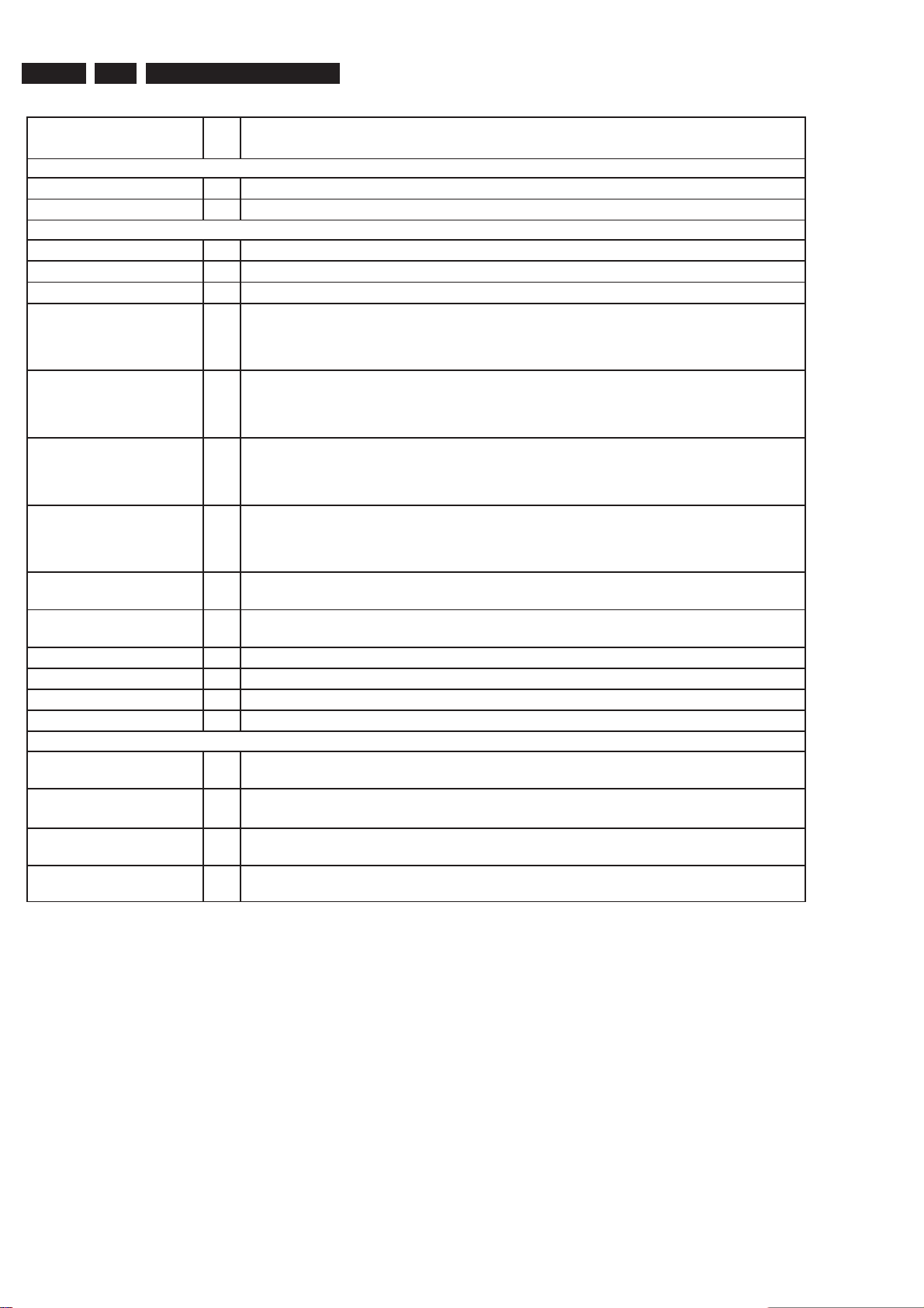
EN 60 3139 785 3220x8.
Circuit- and IC Description
TERMINAL
NAME NUMBER
Host Interface
SCL 28 I I2C clock input
SDA 29 I/O I2C data bus
Power Supplies
AGND 26 I Analog ground. Connect to analog ground.
A18GND_REF 13 I Analog 1.8-V return
A18VDD_REF 12 I Analog power for reference 1.8 V
CH1_A18GND
CH2_A18GND
CH3_A18GND
CH4_A18GND
CH1_A18VDD
CH2_A18VDD
CH3_A18VDD
CH4_A18VDD
CH1_A33GND
CH2_A33GND
CH3_A33GND
CH4_A33GND
CH1_A33VDD
CH2_A33VDD
CH3_A33VDD
CH4_A33VDD
DGND
DVDD
IOGND 39, 49, 62 I Digital power return
IOVDD 38, 48, 61 I Digital power. Connect to 3.3 V or less for reduced noise.
PLL_A18GND 77 I Analog power return
PLL_A18VDD 76 I Analog power. Connect to 1.8 V.
Sync Signals
HS/CS/GPIO 72 I/O
VS/VBLK/GPIO 73 I/O
FID/GPIO 71 I/O
AVID/GPIO 36 I/O
79
10
15
24
78
11
14
25
3
6
19
22
4
5
20
21
27, 32, 42,
56, 68
31, 41, 55,
67
I/O
I Analog 1.8-V return
I Analog power. Connect to 1.8 V.
I Analog 3.3-V return
I Analog power. Connect to 3.3 V.
I Digital return
I Digital power. Connect to 1.8 V.
Horizontal sync output or digital composite sync output
Programmable general-purpose I/O
Vertical sync output (for modes with dedicated VSYNC) or VBLK output
Programmable general-purpose I/O
Odd/even field indicator output. This terminal needs a pulldown resistor.
Programmable general-purpose I/O
Active video indicator output
Programmable general-purpose I/O
DESCRIPTION
Page 61
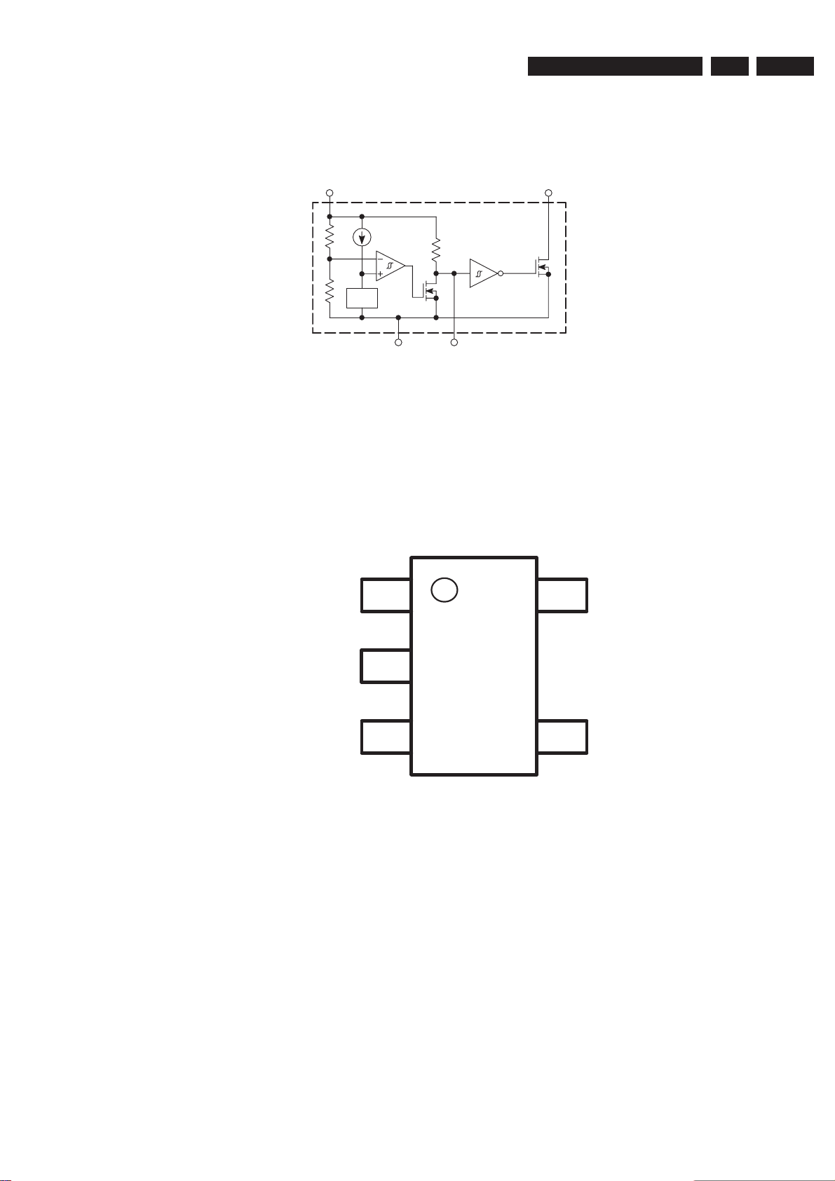
Circuit- and IC description
IC7595 - Voltage Detector Series with Programmable Delay
BLOCK DIAGRAM
EN 613139 785 3220x 8.
Open Drain Output Configuration
2 Input
V
PIN DESCRIPTION AND CONFIGURATION
NCP303LSNxxT1
ref
3 Gnd
PIN CONNECTIONS AND
MARKING DIAGRAM
R
D
5C
D
Figure 8-18
1 Reset Output
Reset
Output
Input
Ground
1
5
xxxYW
2
3
4
xxx = 302 or 303
Y = Year
W = Work Week
(Top View)
C
D
N.C.
Figure 8-19
Page 62
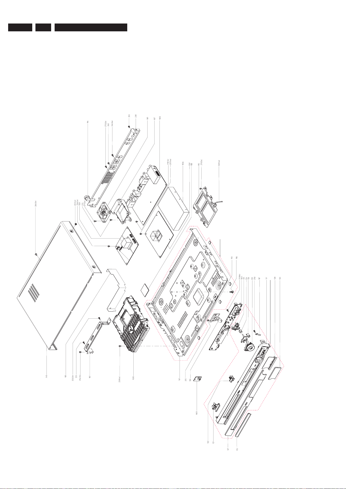
EN 62
9.
3139 785 3220x
Exploded View & Spare Parts List
Exploded View of DVDR3455H/55/97/75
3139_249_36541_110_1_a1.pdf 2006-05-31
P002
P001
Figure 9-1
Page 63
Exploded View & Spare Parts List
MISCELLANEOUS-SET & ACCESSORY
P001 3141 079 39691 FRONT CAB. ASSY DVDR3455H
P001 3141 079 39701 FRONT CAB. ASSY DVDR3455H APAC
/75/96/97
P002 3141 079 36761 FRAME ASSY DVDR3455H
0110 3139 244 10561 COVER TRAY DVDR3455H
0131 3139 241 25081 CLIP ESD DVDR3380
0179 3139 241 25041 SPRING EMC DVDR3400
0180 3139 241 24361 SPRING AV DVDR3400
0184 4822 532 60948 BUSH
0189 2822 031 00051 FAN 12VDC 0.6W 3000RPM B
0230 3139 241 24101 PLATE REAR DVDR3455H NAFTA
0240 3139 241 24231 COVER TOP DVDR3455H
0269 2522 200 98475 SCR PAN TORX ST BK #6-32X6
0341 2422 549 00971 REMOTE CONTR DVDR3455H/NAFTA
B
0345 2422 070 00026
MAINS CORD BRZ 10A 1M85 VH B
0345 4822 321 11499 MAINSCORD 2.0M - EU
/55
/55
/97
3139 785 3220x
9.
EN 63
0345 2422 070 98233 MAINSCORD AUS 7A5 1M8 VH BK B
0345 2422 070 00093 MAINSCORD TWN 7A 1M8 VH BK B
0346 3139 128 73010 MAINS PLUG ADAPTER
/75
/96
/55
0350 2422 076 00718 CBLE CINCH 1M5 CINCH RDYEWH B
0487 4822 320 50377 CONNECT. CABLE PAL
1001 3139 248 88731 PCBAS DVDR3455H DIGI BOARD LA
1001 3139 248 51321 PCBAS DVDR3455H DIGI BOARD/75
1001 3139 248 88721 PCBSA DVDR3455H DIGI BOARD/97
1001 3139 248 51311 PCBAS DVDR3455H DIGI BOARD
/55
/75
/97
/96
1002 3139 248 88701 PCBAS DVDR3455H ANA BOARD NA
/55/96
1002 3139 248 88691 PCBAS DVDR3455H ANA BOARD AP
/75/97
1003 3139 248 89111 PCBAS DVDR3455H FRONT COMBI
1004 3139 247 12862
PSU 06H85 WR AC7012X LF PIE
1005 3139 248 00221 DRIVE D5.1 CLOSED
1006 2822 062 00142 HDD 3.5”” 160GB WD1600BB-55GUC0
8003 3139 241 02541 FFC FOIL 18P/180/18P AD 1MMP
8004 3139 241 02551 FFC FOIL 19P/180/19P AD 1MMP
8005 3139 241 02531 FFC FOIL 24P/140/24P AD 1MMP
8006 3139 241 02061 CBLE HR 04P/120/04P LC UL
8007 3139 241 02361 CBLE EH 04P/220/04P F6001 UL
8008 3139 241 02181 FFC FOIL 14P/280/14P BD 1MMP
8009 3139 241 02161 CBLE IDE 40P/220/40P IDE UL SP
8010 3139 241 00921 CBLE IDE 40P/280/40P IDE UL
8011 3139 241 01521 FFC FOIL 09P/280/09P BD 1MMP
8013 3139 241 02241 CBLE VH 05P/180/05P VH 22ST BK
Note: Only the parts mentioned in this list are normal service
spare parts.
Page 64

EN 64
10.
3139 785 3220x
10. REVISION LIST
Version 1.0
* Initial Release
Version 1.1
* Addition of DVDR3455H/96
* Update service parts list
Revision List
 Loading...