

Philips DVDR-3440-H Service Manual

2.1 Safety Instructions
2.1.1 General Safety
Safety regulations require that during a repair:
• Connect the unit to the mains via an isolation transformer.
• Replace safety components, indicated by the symbol
,
only by components identical to the original ones. Any
other component substitution (other than original type)
may increase risk of fire or electrical shock hazard.
Safety regulations require that after a repair, you must return
the unit in its original condition. Pay, in particular, attention to
the following points:
• Route the wires/cables correctly, and fix them with the
mounted cable clamps.
• Check the insulation of the mains lead for external
damage.
• Check the electrical DC resistance between the mains
plug and the secondary side:
1. Unplug the mains cord, and connect a wire between
the two pins of the mains plug.
2. Set the mains switch to the ‘on’ position (keep the
mains cord unplugged!).
3. Measure the resistance value between the mains
plug and the front panel, controls, and chassis
bottom.
4. Repair or correct unit when the resistance
measurement is less than 1 MΩ.
5. Verify this, before you return the unit to the customer/
user (ref. UL-standard no. 1492).
6. Switch the unit ‘off’, and remove the wire between the
two pins of the mains plug.
2.1.2 Laser Safety
This unit employs a laser. Only qualified service personnel
may remove the cover, or attempt to service this device (due
to possible eye injury).
Laser Device Unit
Type : Semiconductor laser
GaAlAs
Wavelength : 650 nm (DVD)
: 780 nm (VCD/CD)
Output Power : 20 mW
(DVD+RW writing)
: 0.8 mW
(DVD reading)
: 0.3 mW
(VCD/CD reading)
Beam divergence : 60 degree
CLASS 1
LASER PRODUCT
Figure 2-1
Note: Use of controls or adjustments or performance of
procedure other than those specified herein, may result in
hazardous radiation exposure. Avoid direct exposure to beam.
2.2 Warnings
2.2.1 General
• All ICs and many other semiconductors are susceptible
to electrostatic discharges (ESD,
). Careless handling
during repair can reduce life drastically. Make sure that,
during repair, you are at the same potential as the mass
of the set by a wristband with resistance. Keep
components and tools at this same potential.
Available ESD protection equipment:
– Complete kit ESD3 (small tablemat, wristband,
connection box, extension cable and earth cable)
4822 310 10671.
– Wristband tester 4822 344 13999.
• Be careful during measurements in the live voltage
section. The primary side of the power supply, including
the heatsink, carries live mains voltage when you
connect the player to the mains (even when the
player is ‘off’!). It is possible to touch copper tracks and/
or components in this unshielded primary area, when
you service the player. Service personnel must take
precautions to prevent touching this area or components
in this area. A ‘lightning stroke’ and a stripe-marked
printing on the printed wiring board, indicate the primary
side of the power supply.
• Never replace modules, or components, while the unit is
‘on’.
2.2.2 Laser
• The use of optical instruments with this product, will
increase eye hazard.
• Only qualified service personnel may remove the cover or
attempt to service this device, due to possible eye injury.
• Repair handling should take place as much as possible
with a disc loaded inside the player.
• Text below is placed inside the unit, on the laser cover
shield:
Figure 2-2
2. Safety Information, General Notes & Lead Free Requirements
CAUTION VISIBLE AND INVISIBLE LASER RADIATION WHEN OPEN AVOID EXPOSURE TO BEAM
ADVARSEL
SYNLIG OG USYNLIG LASERSTRÅLING VED ÅBNING UNDGÅ UDSÆTTELSE FOR STRÅLING
ADVARSEL SYNLIG OG USYNLIG LASERSTRÅLING NÅR DEKSEL ÅPNES UNNGÅ EKSPONERING FOR STRÅLEN
VARNING SYNLIG OCH OSYNLIG LASERSTRÅLNING NÄR DENNA DEL ÄR ÖPPNAD BETRAKTA EJ STRÅLEN
VARO! AVATTAESSA OLET ALTTIINA NÄKYVÄLLE JA NÄKYMÄTTÖMÄLLE LASER SÄTEILYLLE. ÄLÄ KATSO SÄTEESEEN
VORSICHT SICHTBARE UND UNSICHTBARE LASERSTRAHLUNG WENN ABDECKUNG GEÖFFNET NICHT DEM STRAHL AUSSETSEN
DANGER VISIBLE AND INVISIBLE LASER RADIATION WHEN OPEN AVOID DIRECT EXPOSURE TO BEAM
ATTENTION RAYONNEMENT LASER VISIBLE ET INVISIBLE EN CAS D’OUVERTURE EXPOSITION DANGEREUSE AU FAISCEAU

2.3 Lead Free Requirement
Information about Lead-free produced sets
Philips CE is starting production of lead-free sets from
1.1.2005 onwards.
INDENTIFICATION:
Regardless of special logo (not always indicated)
One must treat all sets from
1 Jan 2005 onwards, according
next rules.
Example S/N:
Bottom line of typeplate gives a 14-digit S/N. Digit 5&6 is the year, digit 7&8 is
the week number, so in this case 1991 wk 18
So from 0501 onwards = from 1 Jan 2005 onwards
Important note: In fact also products of year 2004 must be treated in this way as long as you
avoid mixing solder-alloys (leaded/ lead-free). So best to always use SAC305 and the higher
temperatures belong to this.
Due to lead-free technology some rules have to be respected by the
workshop during a repair:
• Use only lead-free solder alloy Philips SAC305 with order
code 0622 149 00106. If lead-free solder-pate is required,
please contact the manufacturer of your solder-equipment.
In general use of solder-paste within workshops should be
avoided because paste is not easy to store and to handle.
•
Use only adequate solder tools applicable for lead-free
solder alloy. The solder tool must be able
o To reach at least a solder-temperature of 400°C,
o To stabilize the adjusted temperature at the solder-tip
o To exchange solder-tips for different applications.
• Adjust your solder tool so that a temperature around 360°C
– 380°C is reached and stabilized at the solder joint.
Heating-time of the solder-joint should not exceed ~ 4 sec.
Avoid temperatures above 400°C otherwise wear-out of
tips will rise drastically and flux-fluid will be destroyed. To
avoid wear-out of tips switch off un-used equipment, or
reduce heat.
• Mix of lead-free solder alloy / parts with leaded solder alloy
/ parts is possible but PHILIPS recommends strongly to
avoid mixed solder alloy types (leaded and lead-free).
If one cannot avoid or does not know whether product is
lead-free, clean carefully the solder-joint from old solder
alloy and re-solder with new solder alloy (SAC305).
• Use only original spare-parts listed in the Service-Manuals.
Not listed standard-material (commodities) has to be
purchased at external companies.
• Special information for BGA-ICs:
- always use the 12nc-recognizable soldering temperature
profile of the specific BGA (for de-soldering always use the
lead-free temperature profile, in case of doubt)
- lead free BGA-ICs will be delivered in so-called ‘drypackaging’ (sealed pack including a silica gel pack) to
protect the IC against moisture. After opening, dependent
of MSL-level seen on indicator-label in the bag, the
BGA-IC possibly still has to be baked dry. (MSL=Moisture
Sensitivity Level). This will be communicated via AYSwebsite.
Do not re-use BGAs at all.
•
For sets produced before 1.1.2005 (except products of
2004), containing leaded solder-alloy and components,
all needed spare-parts will be available till the end of the
service-period. For repair of such sets nothing changes.
•
On our website www.atyourservice.ce.Philips.com you
find more information to:
BGA-de-/soldering (+ baking instructions)
Heating-profiles of BGAs and other ICs used in Philips-sets
You will find this and more technical information within the
“magazine”, chapter “workshop news”.
For additional questions please contact your local repair-helpdesk.
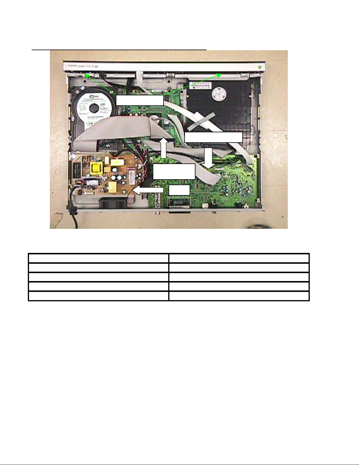
1.Technical Specifications and Connection Facilities
A
Front Board
nalogue Board
Digital Board
PSU
1.1 Read / Write Speed
Type of Disc(Function) Disc Rotation Speed
Read Speed CD 7X CAV
Read Speed DVD 4X CAV
Write Speed DVD+R/RW 2.4X ZCAV
Write Speed DVD-R/RW 2X
1.3 General:
Mains voltage : 220V-240V
Mains frequency : 50Hz
Standby Power consumption : <3W
1.4 RF Tuner
Test Equipment :Fluke 54200 TV Signal generator
Test Stream:PAL BG Philips Standard test pattern
1.4.1.1 System:

PAL B/G, PAL D/K, SECAM L/L’, PAL I
1.4.1.2 RF – Loop Through
Frequency range : 43MHz-860MHz
Gain: (ANT IN-ANT OUT) : -4dB ± 2dB
1.4.1.3 Receiver:
PLL tuning with AFC for optimum reception
Frequency range : 45.25MHz - 857MHz
Sensitivity at 40dB S/N
(video unweighted) : ≤ 40dBµV at 75Ω
(high end)
≤ 60dBµV at 75Ω
(low end)
1.4.1.5 Video Performance:
Channel 25 / 503,25MHz,
Test pattern: PAL BG PHILIPS standard test pattern,
RF Level 74dBV
Measured on SCART 1
Frequency response : 0.1MHz - 4.00MHz ± 3dB
Group delay (0.1MHz-4.4MHz) : 0 nsec ± 150 nsec
1.4.1.6 Audio Performance:
Audio Performance Analogue – HiFi:
Frequency response at SCART 1
(L + R) output : 100Hz -12kHz / 0 ± 3dB
S/N Ratio (20Hz- 20KHz)
unweighted
Harmonic distortion
(1kHz, ± 25kHz deviation) :≤ 1.5%
Audio Performance NICAM:
Frequency response at SCART 1
(L + R) output : 40 Hz – 15 kHz / 0 ± 3dB
S/N according to DIN 45405,7,1967
and PHILIPS standard test pattern
video signal : ≥ 40dB
Harmonic distortion (1kHz) : ≤ 1.5%

1.4.1.7 Tuning
Automatic Search Tuning
scanning time without antenna : 3min. typical
stop level (vision carrier) : ≥ 37dBµV
Maximum tuning error(drift) during
operation : ± 100kHz
Tuning Principle
Automatic B, G, I, DK and L/L’ detection .Manual selection in “STORE” mode
1.5 Analogue Inputs / Outputs
1.5.1 SCART 1(Connected to TV)
Pin Signals:
1 - Audio-out R 1.8V RMS
2 - Audio-out R
3 - Audio-out L 1.8V RMS
4 - Audio GND
5 - Blue / Chroma GND
6 - Audio- in L
7 - Blue-out 0.7Vpp ± 0.1V into 75 W
8 - Function switch < 2V = TV
> 4.5V / < 7V = asp. Ratio 16:9 DVD
> 9.5V / < 12V = asp. Ratio 4:3 DVD
9 - Green GND
10 – P50 control not use
11 – Green out 0.7Vpp ± 0.1V into 75W (*)
12 - NC
13 - Red / Chroma GND
14 - Fast switch GND
15 - Red-out / Chroma-out 0.7Vpp ± 0.1V into 75W (*)
16 - Fast switch
RGB / CVBS or Y out < 0.4V into 75W = CVBS
>1V / < 3V into 75W = RGB
17 - Y/CVBS GND OUT
18 - CVBS GND IN
19 - CVBS-out 1Vpp ± 0.1V into 75W(*)
20 - CVBS-in
21 - Shield
1.5.2 SCART 2 (Connected to AUX)

Pin Signals:
1 - Audio-out R 1.8V RMS
2 - Audio-in R
3 - Audio-out L 1.8V RMS
4 - Audio GND
5 - Blue / Chroma GND
6 - Audio-in L
7 - Blue-in
8 - Function switch
9 - Green GND
10 - NC
11 - Green-in
12 - NC
13 - Red / Chroma GND
14 - Fast switch GND
15 - Red-in/Chroma-in
16 - Fast switch
RGB / CVBS or Y in
17 - CVBS-OUT GND
18 – Y/CVBS in GND
19 - CVBS out sync 1Vpp ± 0.1V into 75Ω
20 – CVBS in / Y-in
21 – Shield
1.5.3 Audio/Video Front Input Connectors
Audio – Cinch
Input voltage : 2.2Vrms
Input impedance : > 10kΩ
Video – Cinch
Input voltage : 1Vpp ± 3dB
Input impedance : 75Ω
Video – YC (Hosiden)
According to IEC 933-5
Superimposed DC-level on pin 4(load >100kΩ)
<2.4V is detected as 4:3 aspect ratio
>3.5V is detected as 16:9 aspect ratio
Input voltage Y : 1Vpp ± 3dB
Input impedance Y : 75Ω
Input voltage C : 300 mVpp ± 3dB
Input impedance C : 75Ω

1.6 Digital Inputs / Outputs
1.6.1 Digital Output
Digital Audio – Coaxial
LCM : according IEC 60958
MPEG 1,MPEG2,AC3 : according IEC 61937
DTS : according IEC 61937+addendum
1.7.3 Digital Video Input(IEEE 1394)
Implementation Standard according:
IEEE Std 1394-1995
IEC61883 - Part1
IEC61883 - Part2 SD-DVCR (02-01-1997)
Specification of consumer use digital VCR’s using 6.3mm magnetic tape – dec.
1994
Mechanical connection according to Annex of IEC 61883-1
1.8 Video Performance
All outputs loaded with 75 Ω
SNR measurements over full bandwidth without weighting.
1.8.1 SCART (RGB)
SNR : > -65dB on all output
Bandwidth : 4.8MHz ± 2dB
1.9 Audio Performance CD
1.9.1 Cinch Output Rear
Output voltage 2 channel mode : 2Vrms ± 2dB
Channel unbalance (1kHz) : < 0.22dB
Crosstalk 1kHz : > 100dB
Crosstalk 16Hz-20kHz : > 87dB
Frequency response 20Hz-20kHz : ± 0.5dB max
Signal to noise ratio : < 85dB
Dynamic range 1kHz : <83dB
Distortion and noise 1kHz : < 83dB
Distortion and noise 16Hz-20kHz : < 75dB
Intermodulation distortion : < 70dB
Mute : < 95dB

1.9.2 Scart Audio
Output voltage 2 channel mode : 1.6Vrms ± 2dB
Channel unbalance (1kHz) : < 1dB
Crosstalk 1kHz : > 85dB
Crosstalk 16Hz-20kHz : > 70dB
Frequency response 20Hz-20kHz : ± 0.5dB max
Signal to noise ratio : > 80dB
Dynamic range 1kHz : > 75dB
Distortion and noise 1kHz : > 75dB
Distortion and noise 16Hz-20kHz : > 50dB
Intermodulation distortion : > 70dB
Mute : > 80dB
Height of feet : 5.5mm
Apparatus(WxDxH) : 435 x 65 x 340 mm
Weight without packaging : 4.3 kg
Weight with packaging : 6.0kg
1.10 Laser Output Power & Wavelength
1.10.1 DVD
Output power during reading : 0.8mW
Output power during writing : 20mW
Wavelength 650nm
1.10.2 CD
Output power :0.3mW
Wavelength :780nm
1.11 Supported disc type and media speed
Disc Media Speeds
DVD+R 1x - 16x
DVD+RW 2.4x - 4x
DVD -R 1x - 16x
DVD -RW 2.4x - 4x
DVD+R DL 2.4x
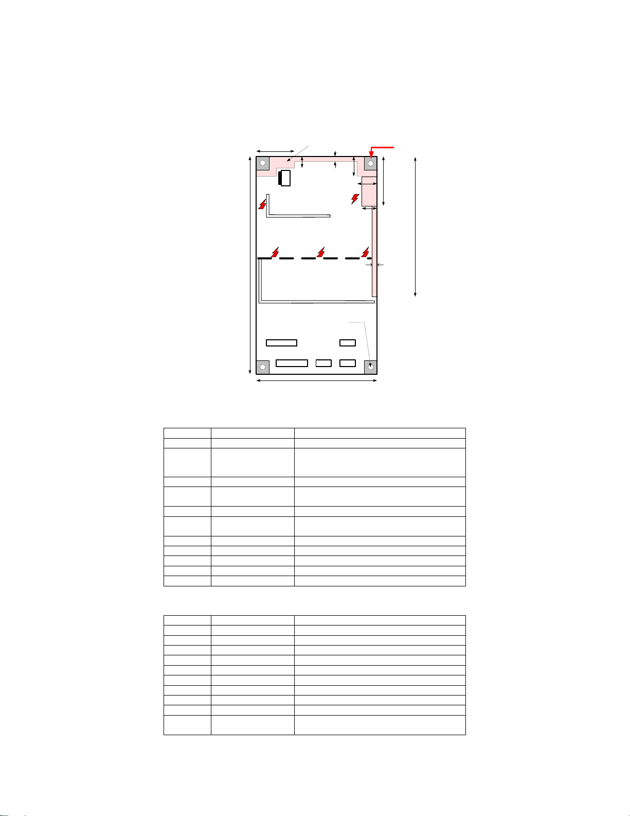
1.1. PSU Board
1.1.1. General
No component, No copper
30.5+/-0.15
170+/-0.2
Keep 10x10 area as base of
track area
9+/-0.1
Y
R
Mains connector
A
M
I
R
P
Dia=3.2+/-0.05 (4x)
metal plate for screws
4+/-0.1
16+/-0.1
A
D
B
95+/-0.15
The PSU board provides the following connection to the rest of the set:
• Connector A: Supply/Signal to Analog Board
Pin no. Supply / Signal Remarks
1 12VSTBY
2 STBY control >2.5V = supply for conn. B is off (Standby
mode)
<0.5V = supply for conn. B is on (On mode)
3 5VSTBY
4 DD_ON >2.5V = supply for conn. D is on
<0.5V = supply for conn. D is off
5 3V3STBY
6 IPFAIL >4.0V = power is good
<0.5V = power fail
7 5NSTBY
8 GND
9 33VSTBY
10 GND
11 VGNSTBY
• Connector B: Supply to Digital Board
Pin no. Supply / Signal Remarks
1 3V3D
2 3V3D
3 3V3D
4 3V3D
5 GND
6 12VD
7 GND
8 GND
9 5VD
10 HD_ON >2.5V = supply for conn. C & G is on
<0.5V = supply for conn. C & G is off
16+/-0.1
12+/-0.1
C
This screw can
be used as EMC
Y-capacitor
connection
39+/-0.1
110+/-0.1
3.5+/-0.1
G

11 GND
• Connector C: not in use
• Connector D: Supply to Basic Engine
• Connector E: Supply to HDD
! The Mains must be disconnected from the Set before attempting the procedure mentioned below:
The PSU is designed with short-circuit protection that will shutdown the power supply. When this happen, the
voltage stored in capacitor C1 and C2 will prevent the Power Supply to turn-on, therefore they must be
discharged with a screwdriver with high electrical isolation handle before the PSU can function normally again.
Note :During the process of discharging the capacitors ,spark can be observed which is typical of the high
voltage stored in Capacitor C1 and C2.
12 5ND
Pin no. Supply
1 12VE
2 GND
3 GND
4 5VE
Pin no. Supply
1 12VH
2 GND
3 GND
4 5VH
 Loading...