Philips DVDR-3435-H, DVDR-3425-H Service Manual
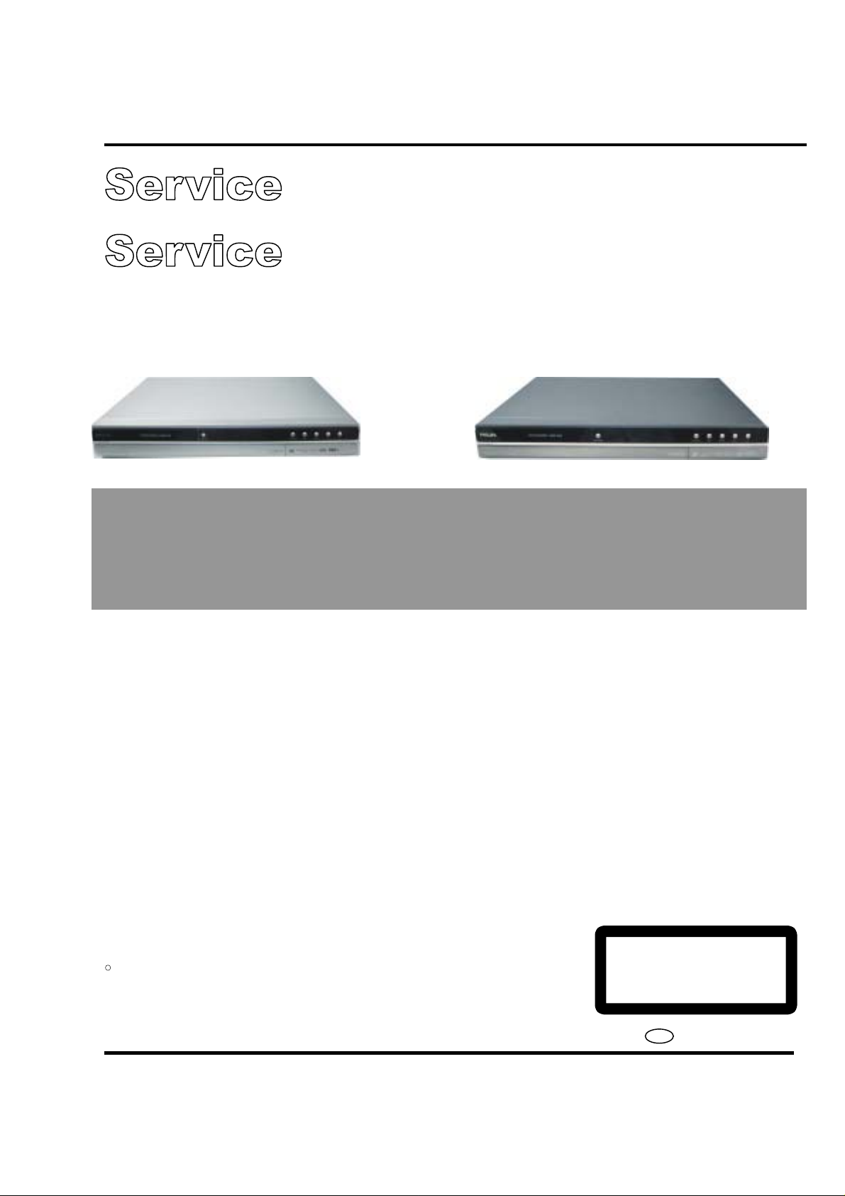
DVD Recorder DVDR3425H, DVDR3435H
A
DVDR3425H/93
DVDR3435H/93
Service
Service Manual
TABLE OF CONTENTS
Page
C
Copyright 2006Philips Consumer Electronics B.V. Eindhoven, The Netherlands
ll rights reserved. No part of this publication may be reproduced, stored in aretrieval system or
transmitted, in any form or by any means, electronic, mechanical, photocopying, or otherwise
without the prior permission of Philips.
3139 785 31930
Published by TCL-KC 0623 Service Audio Printed in The Netherlands Subject to modification
Version 1.0
. Technical Specifications………………………………………….......1-2
. Mechanical and Dismantling Instructions…………………..............2-1
. Region Code, Software Version& Upgrades………………………..3-1
. Trouble Shooting Chart………………………………………………..4-1
. Block and Wiring Diagram…………………………………….….......5-1
. Electrical Diagrams and Print-layouts……………………….……….6-1
. Set Mechanical Exploded view…………………………….………....7-1
. Parts List……………….…………………………………….....…...…8-1
. Revision List……………………………………….……………..........9-1
CLASS 1
LASER PRODUCT
GB
PHILIPS

Technical Specifications
1-2
Video Recording
Recording System: PAL / NTSC
Compression formats: MPEG2
Modes of Record Quality
High Quality: HQ
Standard Play: SP
Standard Play Plus: SP+
Long Play: LP
Extended Play: EP
Super Long Play: SLP
Super Extended Play: SEP
Recording enhancements:
Auto Chapter Marker Insertion, Divide Title, Erase, Manual
Chapter Marking, One Touch Record
Audio compression: Dolby Digital
Video Playback
Disc Playback Media: CD, CD-R / CD-RW, DVD, DVD-Video,
DVD+R, DVD+RW, DVD-R, DVD-RW,MP3-CD,Video CD,
SVCD
Compression formats: MPEG2, MPEG1, MPEG4, DivX
Video Disc Playback System: PAL, NTSC
Audio Playback
Disc Playback Media: MP3-CD, CD, CD-R / CD-RW
Compression formats: Dolby Digital, DTS, MP3, PCM
MP3 Bit Rates: 32~256Kbps
Still Picture Playback
Disc Playback Media: Picture CD
Picture compression format: JPEG
Picture enhancement: Rotate, Zoom, Slideshow
TV Systems
Playback: PAL/NTSC
Recording: PAL/NTSC
Internal tuner: PAL
Video Performance
D/A Converter: 10Bit, 54MHz
A/D Converter: 10Bit, 27MHz
Picture Enhancement: Progressive Scan
Audio Performance
DA Converter 24Bit, 192KHz
AD converter 24Bit, 96KHz
Signal / Noise (1KHz) 90dB
Dynamic range (1KHz) 80dB
Crosstalk (1KHz) 90dB
Turner/Reception/ Transmission
Receive TV Signal: PAL (This set does not support NTSC)
Aerial Input: 75 ohm coaxial (IEC75)
Storage Media
Recording:
- DVD+R, DVD+RW, DVD-R, DVD-RW
Hard Disk Capacity:
- DVDR3425H: 160GB - DVDR3435H: 250GB
HDD Recording enhancements:
- Instant Replay, Time Shift Buffer
Extra Hard Disk Technology:
- Pause Live TV, Simultaneous Record and Playback, Direct
Record to DVD
HDD to DVD archiving: High Speed (Direct Copy)
Connectivity
Rear Connections
- S-video IN/OUT
- Video (CVBS) IN/OUT
- Analog audio Left / Right out (Only for DVDR3425H)
- Analog audio 5.1 out (Only for DVDR3435H)
- Antenna in
- TV out
- Digital audio out
DVDR3425H: COAXIAL; DVDR3435H: COAXIAL,OPTICAL
- Analog audio Left / Right in
- YpbPr Video OUT
- YPbPr Video IN/OUT (Only for DVDR3435H)
* Hint: This set can support progressive and interleaved output but
do not support progressive input
Front Connections
- I.LINK DV in (4 1394 4-pin)
- S-Video in
- Video (CVBS) in
- Analog audio left / right in
- USB in
Timer Recording
Programmable events: 20
Repeat modes: Once, Daily, Weekly, Mon-Fri, Mon-Sat, Weekend
Enhancement: Manual Timer
Convenience
Direct Record to optical disc
Child Protection: Parental Control
Power
Power Supply: 110~240 V; 50~60 Hz
Power Consumption: 36 W
Standby power consumption: <5.0W
Dimensions :
Set Dimensions (W X H X D): 430 X 57 X 340mm
Set Weight : 4.4 Kg
2-1
Mechanical and Dismantling Instructions
Dismantling Instruction
The following guidelines show how to dismantle the
recorder.
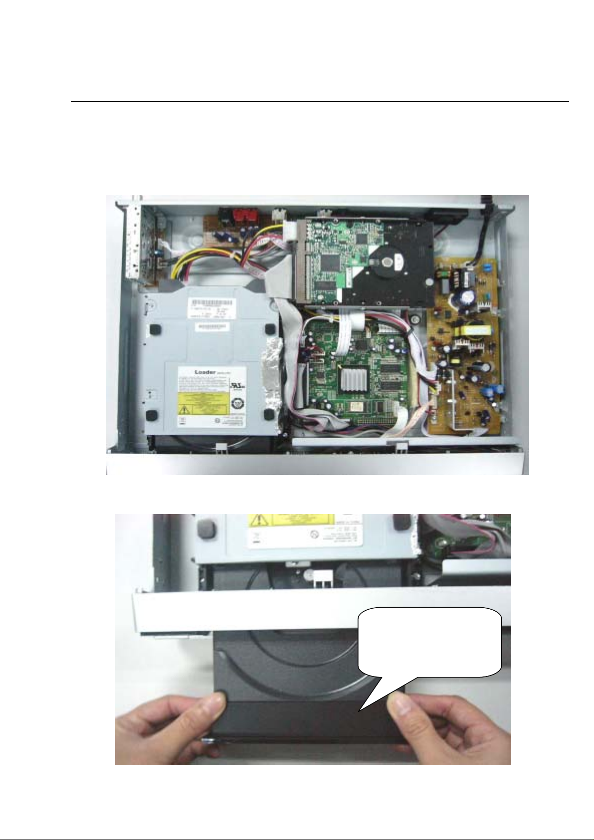
Step1: Remove the 8pcs of screw around the top cover.
And remove top cover. (Figure 1)
Step2: If it is necessary to dismantle Loader or Front Panel. It
should be remove the Front door assembly first. (Figure 2)
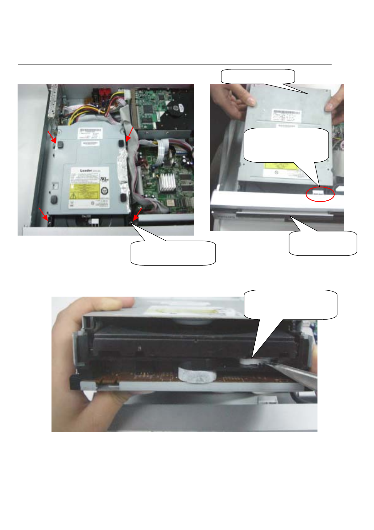
And if the tray can’t open in normal way, you can make it
through the instruction as figure 3 & 4& 5
Note: Make sure to operate gently otherwise it would be
damaged
Figure 1
Figure 2
Please kindly note that dismantle
the front door assembly carefully
to avoid damage tray and the
front door assembly.
2-2
y
Mechanical and Dismantling Instructions
Dismantling Instruction
Figure 3
Remove the screws on both
sides of the loader
Figure 5
Uplift the bottom of loader
When uplift the loader, please
carefully to avoid damage the
front panel support
Figure 4
Push it gently, and the tray will
flick out automatically
The front door assembly
will fall off automaticall
2-3
Mechanical and Dismantling Instructions
Dismantling Instruction
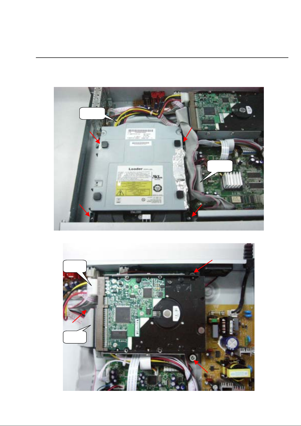
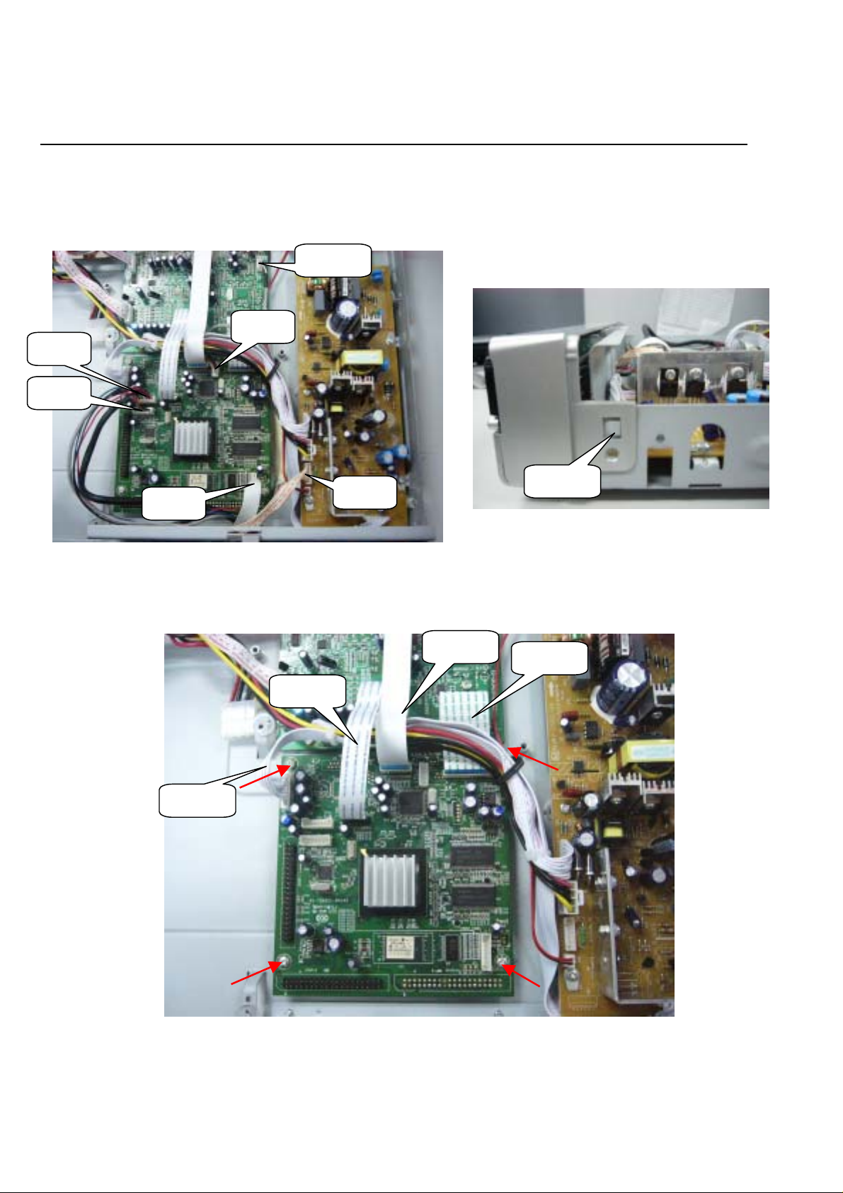
Step3: Dismantling Loader. First, disconnect the 2
connectors aiming in the figure, and then remove the 4
screws on both sides of the loader. (Figure 6)
CON 3
CON 4
CON 1
Step4: Dismantling Hard Disk. disconnect the relative
connectors, and the relative screws, then remove the Hard
Disk. (Figure 7)
Figure 6
Figure 7
CON 2
2-4
Mechanical and Dismantling Instructions
Dismantling Instruction
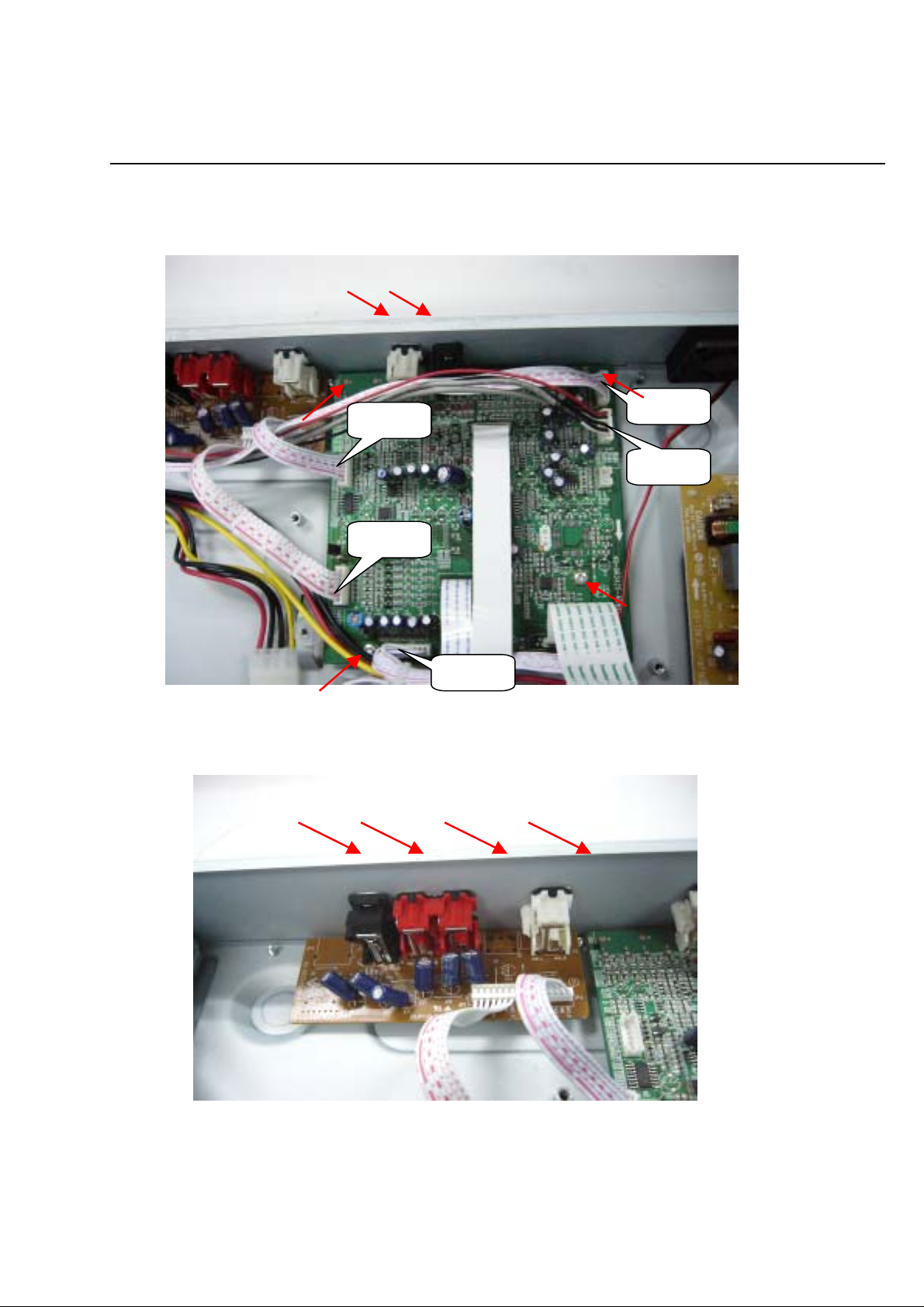
Step5: Dismantling the Front Panel. Disconnect the
relative connectors , and remove the relative screws on
the bottom of the cabinet, then release the snaps on the
both sides of front panel, finally gently pull the panel out
from the set. (Figure 8 & 9)
CON 10
CON 5
CON 9
CON 6
CON 7
CON 8
Figure 8
CON 11
CON 12
Step6: Dismantling Main Board, first disconnect the 4
connectors ,then remove the relative screws. (Figure 10)
CON 13
Figure 10
Snap 1
Figure 9
CON 14
2-5
Mechanical and Dismantling Instructions
Dismantling Instruction
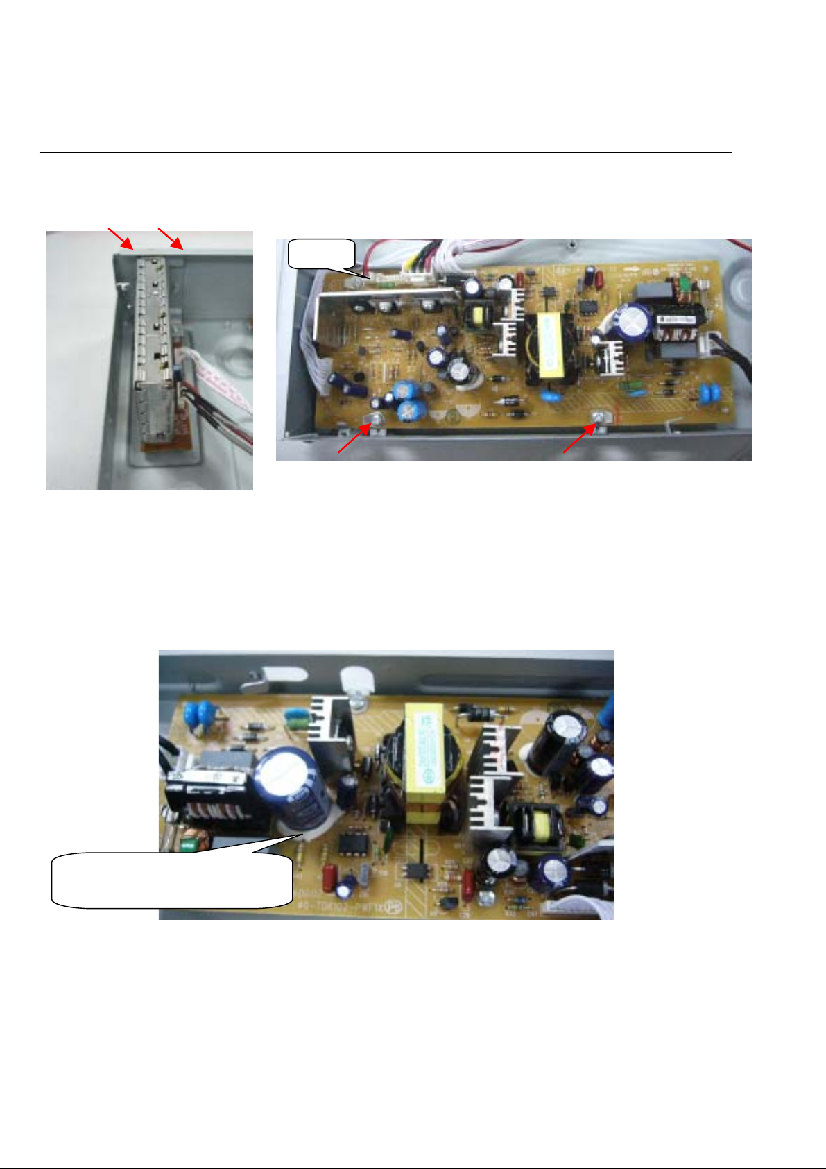
Step7: Dismantling AV Board. first disconnect the 5
connectors, and then remove the relative screws.
(Figure 11)
CON 19
CON 18
CON 17
Figure 11
Figure 12
Step8: Remove the 4pcs of the screws on the back of the cabinet,
then dismantling the OUTPUT Board. (Figure 12)
CON 15
CON 16
2-6
A
Mechanical and Dismantling Instructions
Dismantling Instruction
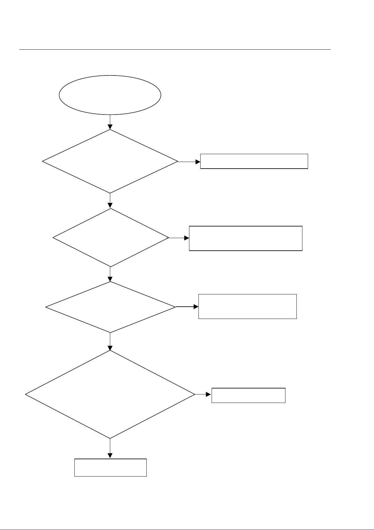
Step9: Remove the 2pcs of the screw on the back of
the cabinet, then dismantling Tuner Board. (Figure
13)
Figure 13
CON 20
Step10: Dismantling Power Board. first disconnect
the connector, then remove
(Figure 14)
the relative screws.
Figure 14
Step11: Make sure adding silicon glue to fix the capacitor after repairing. (Avoid the hazard of capacitor touching the top
cover Figure 15)
dd Silicon glue or Heat glue to fix
Capacitor keep this status
Figure 15

3-1
Region Code, Software Version& Upgrades
Software upgrade
A. Preparation to upgrade software
1) Start the CD Burning software and create a new CD
project (Data Disc) with the following setting:
Label: _____ (No need the label name)
File System: ISO9960
File Name: DVDR3425_93_V*.CUB (For
DVDR3425H/93)
DVDR3435_93_V*.CUB (For
DVDR3435H/93)
Remark: “
Note: It is required capital letter for the Label name
& the File System name.
2) Burn the data onto a blank CDR
B. Procedure for software upgrade:
1) Power up the set and insert the prepared Upgrade
CDR.
2) The set will start reading disc & response with the
following display on TV screen:
Software upgrade disc DETECTED, select OK to
start upgrading or CANCEL to exit.
Press OK to start.
3) After press <OK> button to confirm, then screen will
display:
Upgrading software, please wait. Do not switch off
the power……
Please wait patiently, approximately two minutes
later the upgrading will complete.
4) The upgraded disc will automatically out when the
upgrading complete, and the TV will display:
System is successfully upgraded, Remove disc
from the tray and reset system.
5) According to the TV direction, take out the disc and
press OK, the tray door will close, Reset the
system.
” stand for the upgraded version number
*
C. Read out the software versions to confirm upgrading
1) Power up the set and press <Setup> button on the remote
control.
2) Press <9><9><9><9> <OK> button.
The software version and other information are display on
the TV screen as follows:
Build: XXXXXX-XXXXXXX-XX-XXX
Date: XXXX XX XXXX
Release Version: XXXXX/93_Vxx
Loader Version: VER XXXX
Macrovision version: VXXX
Region Num: XXX
Developer: XXX XX XXXX
D. Replace the new HDD
After finish the replacing of new HDD (Unformatted HDD) in
set and start the set first time, the set will search all hardwares
which are the components of the set automatically and if the set
find the HDD unformatted, it will format it automatically then can
work normally.
Caution: The set must not be power off during
upgrading, in that case the decoder board will
be damaged entirely.
4-1
No display on VFD, and buttons do not work
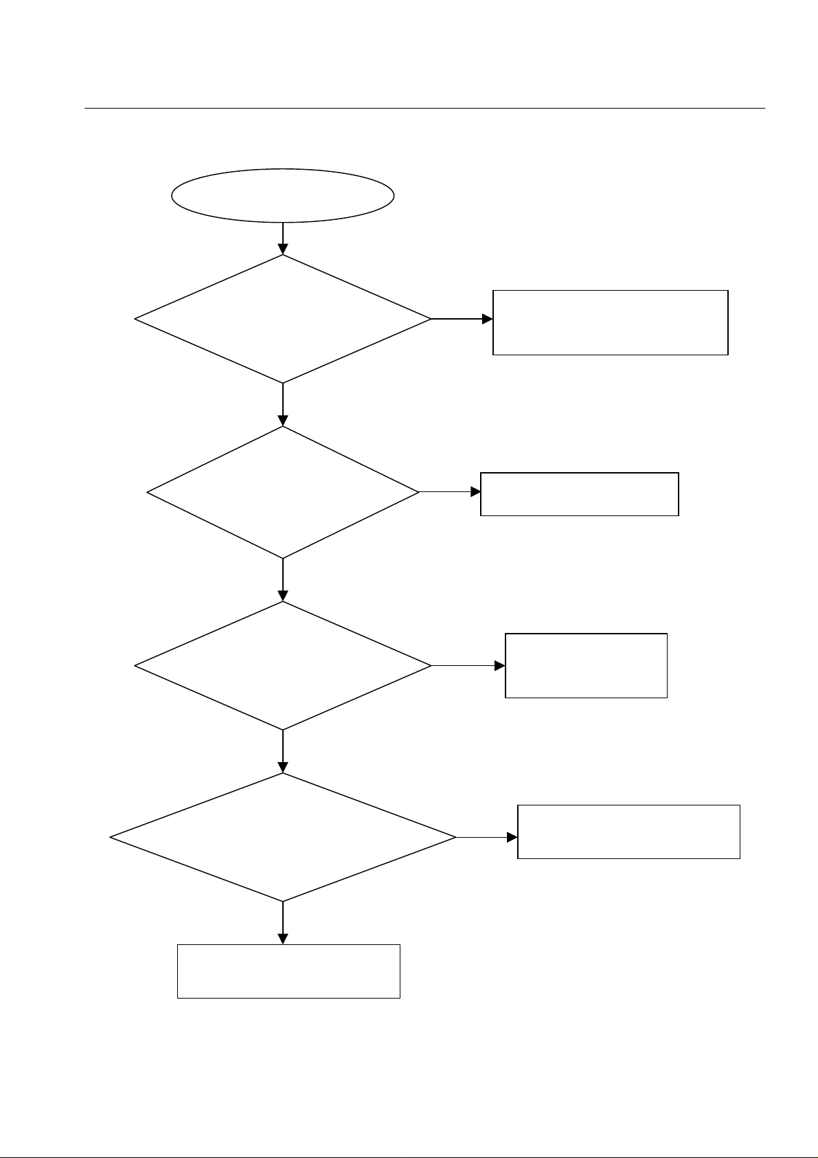
Trouble shooting chart
No display on VFD, and
buttons do not work
Yes
Check every supply
voltage on main board is
normal
No
Refer to Power supply board part
Yes
Check-24V+12V,VCC(
+5v) voltage on the
power and front board
No
Fix the connection JP1 on front board
and CN1 on power board
Yes
Check the front board
signals SCK,SDA, STB
No
Check the U3’s pin 2,4,8 arrive the
U2’s pin 6,8,9 connect condition
Yes
1.Check whether bad solder exists
on U2 and pins of VFD,
2.Check whether the circuit
connected to K2, K3, K4, K5, K6,
K8and K9 is broken.
No
Correct connection
Yes
Replace U2 or VFD
f
4-2
Trouble shooting chart
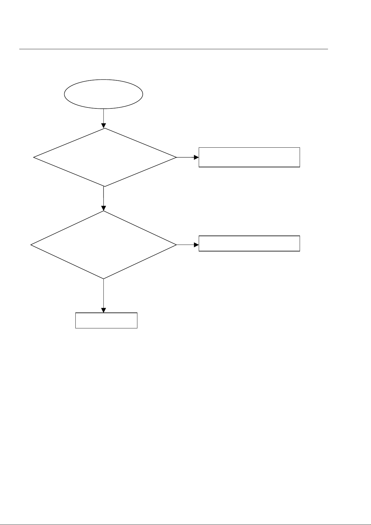
No digital audio output
No digital audio output
Go
Check the FB8 (digital audio) on
the output board is normal.
Yes
No
Fix the connection XP4 on AV board
and JP2 on output board
Yes
Check the R65 (digital
audio ) on the AV
board is normal.
No
Check / Replace R68、C75.
Yes
Check the PIN14 o
Yes
U8 on the AV board is
+5V
No
Check the +5V power
supply on the AV board
Check the P1 of U8 (digital
audio) on the AV board is
normal.
Yes
No
Check P26 of JP2 on main board
signals is normal
Yes
Fix the connection XP3 on AV board
and JP2 on main board
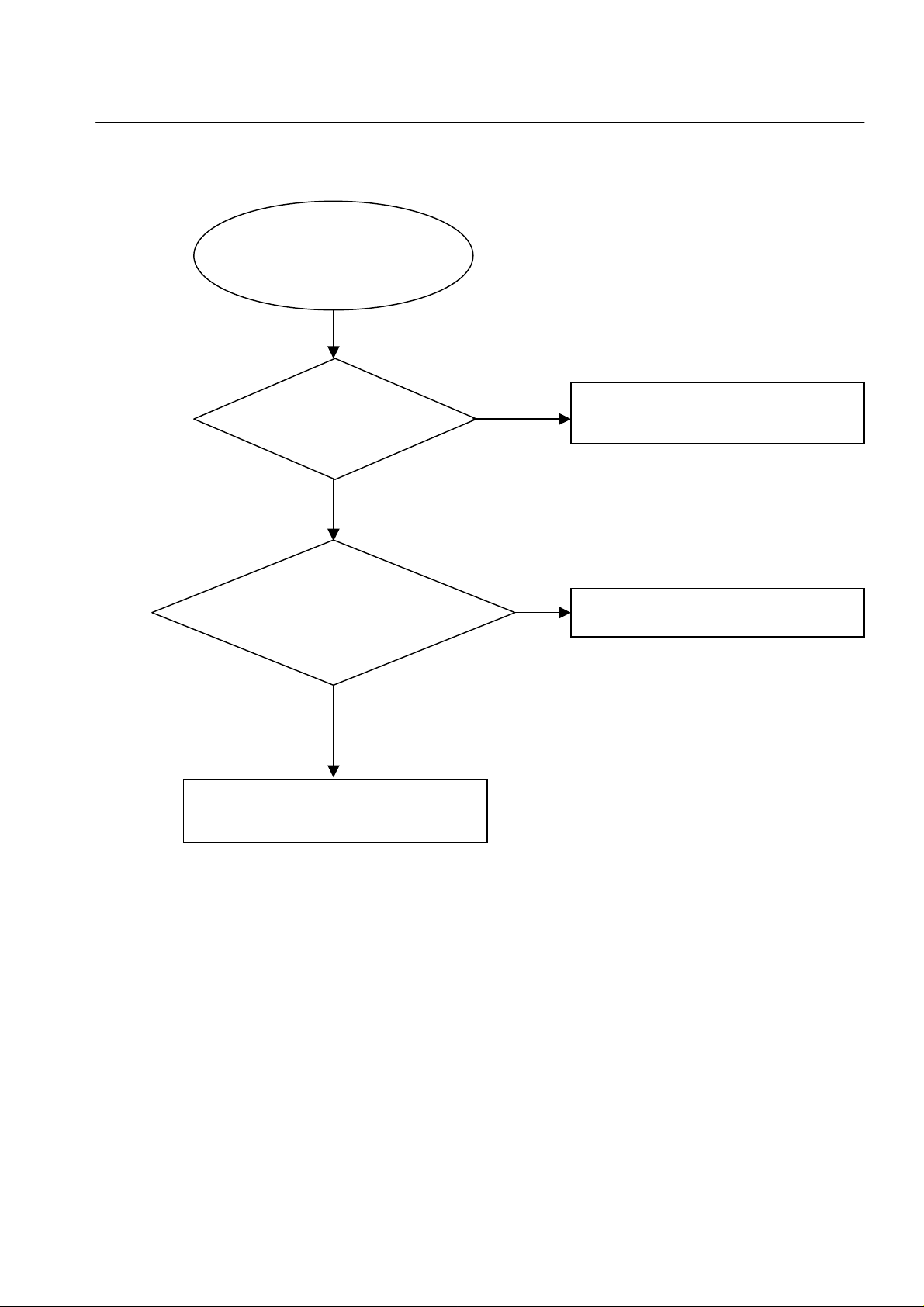
Remote control does not work
Remote control
does not work
Go
Check whether keys on
the front board work or not.
Yes
Check the front board
whether P1 of U4 has
signal when pressing key
on the remote
Yes
Replace U3.
4-3
No
No
Yes
Replace U2 on the power board
Replace U4 on the power board
Trouble shooting chart
t
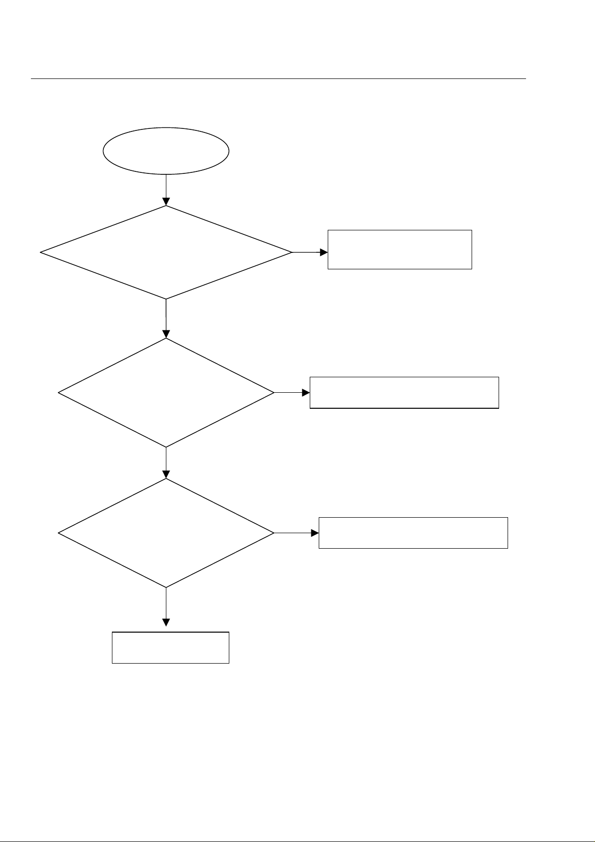
Can’t read disc or can’t open the disk door
Can’t read disc or can’
open the disk door
GO
Check whether the
DVD loader running is
normal
Yes
Check 40pin cable from
main board connection to
the loader is normal
Yes
Check the peripheral components near the
J3 on the main board.
4-4
Trouble shooting chart
NO
NO
Check the connection of the 4PIN cable
from CN6 on the Power Board.
Fix the connection the 40pin cable
4-5
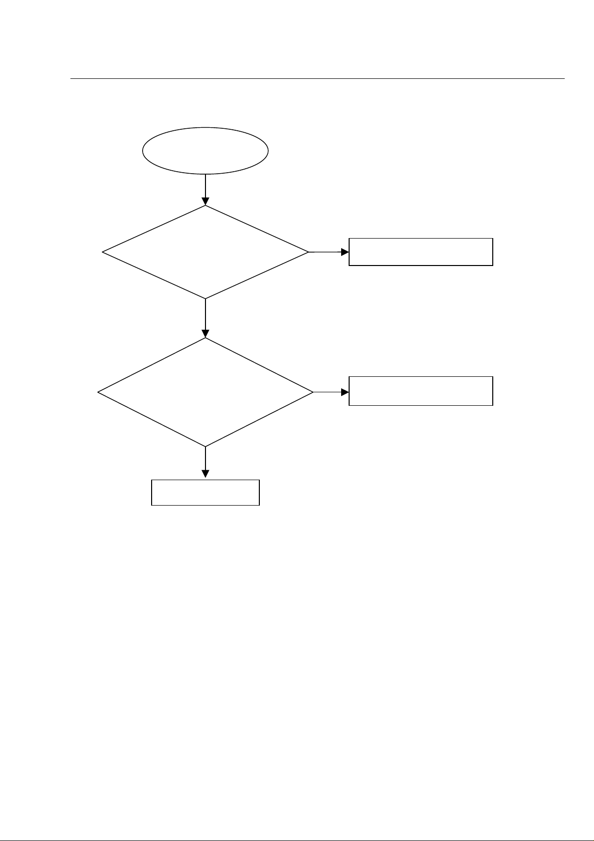
No VFD display
No VFD display
Go
Check whether the voltage
+12V/+5V on the front board
is normal work or not.
Yes
Check whether the
voltage between VFD
F1&VFD F2 is AC3V
Yes
No
No
Fix the connection power board
CN1& front board JP2
Check DC12V to AC 3V switch circuit
Trouble shooting chart
Check whether the
voltage -24V is normal
Replace U2 or VFD.
No
Check the FB2 on the front board
r
4-6
Fan don’t work
Fan don’t work
Go
Check on power board
whether P1 of CN3 is
+12V
No
Check R6 on power board
Yes
Check the cable
connection fan to powe
board CN3
No
Replace the cable
Yes
Trouble shooting chart
Replace Fan
5-1
5-1
A
B
C
D
E
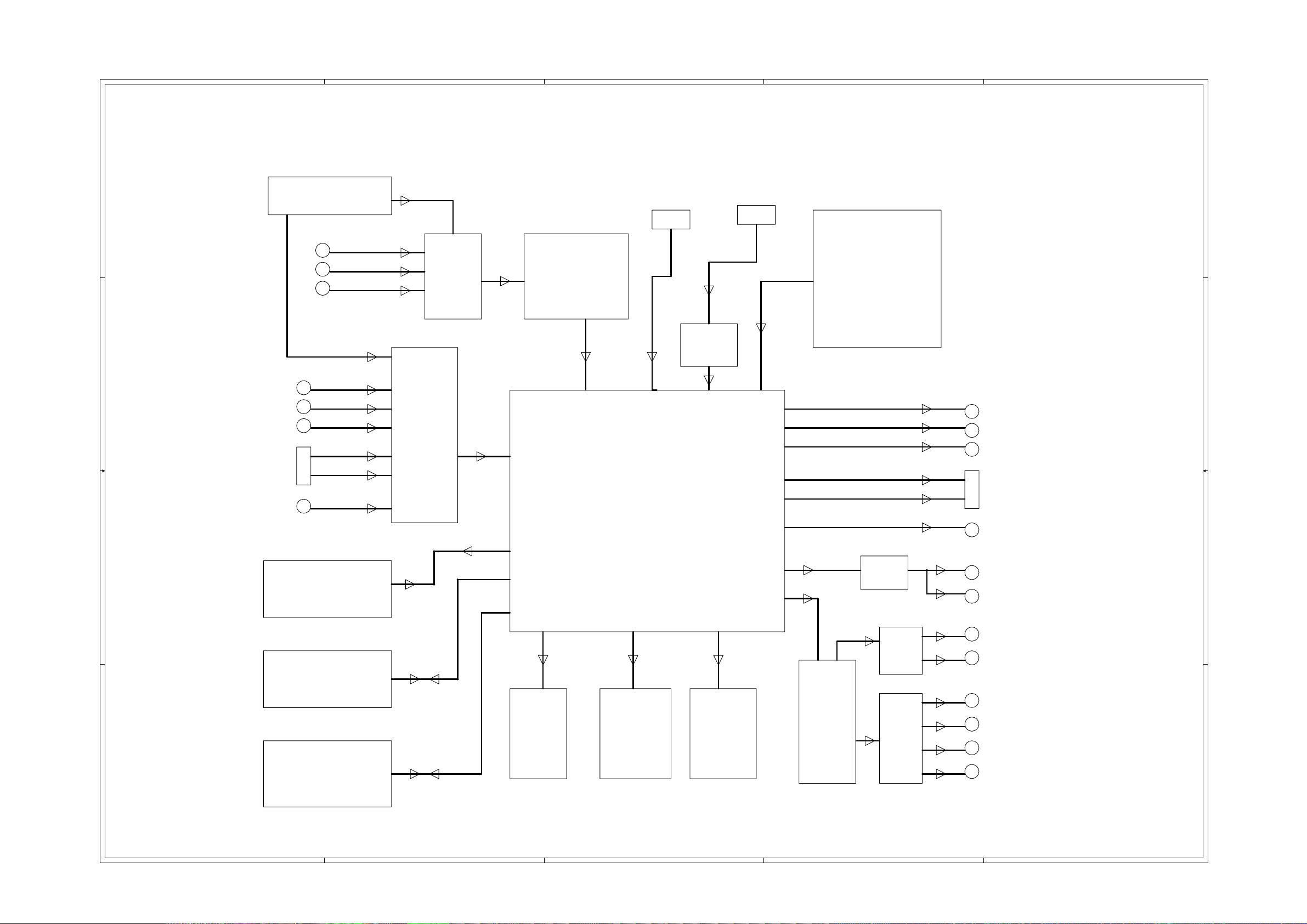
DVDR3425H/93 Block Diagram
4 4
TUNER
AUDIO IN 1
AUDIO IN 2
AUDIO
SW
USB
CS5340
AUDIO ADC
1394
PHY
3 3
TUNER
VIDEO
Y
DECODER
1EEE1394
POWER
Y
Pb
C
CVBS
Pr
Y
C
DMN8652
CVBS
RW LOAD ATAPI
2 2
HDD 160G
BUFFER
CS4382
FORNT
FLASH
SDRAM*1
SDRAM*2
AUDIO
DAC
PANEL KEY
IR & VFD
1 1
COAX
AUDIO LCH
AUDIO RCH
BUFFER
A
B
C
D
E
5-2 5-2
5
4
3
2
1
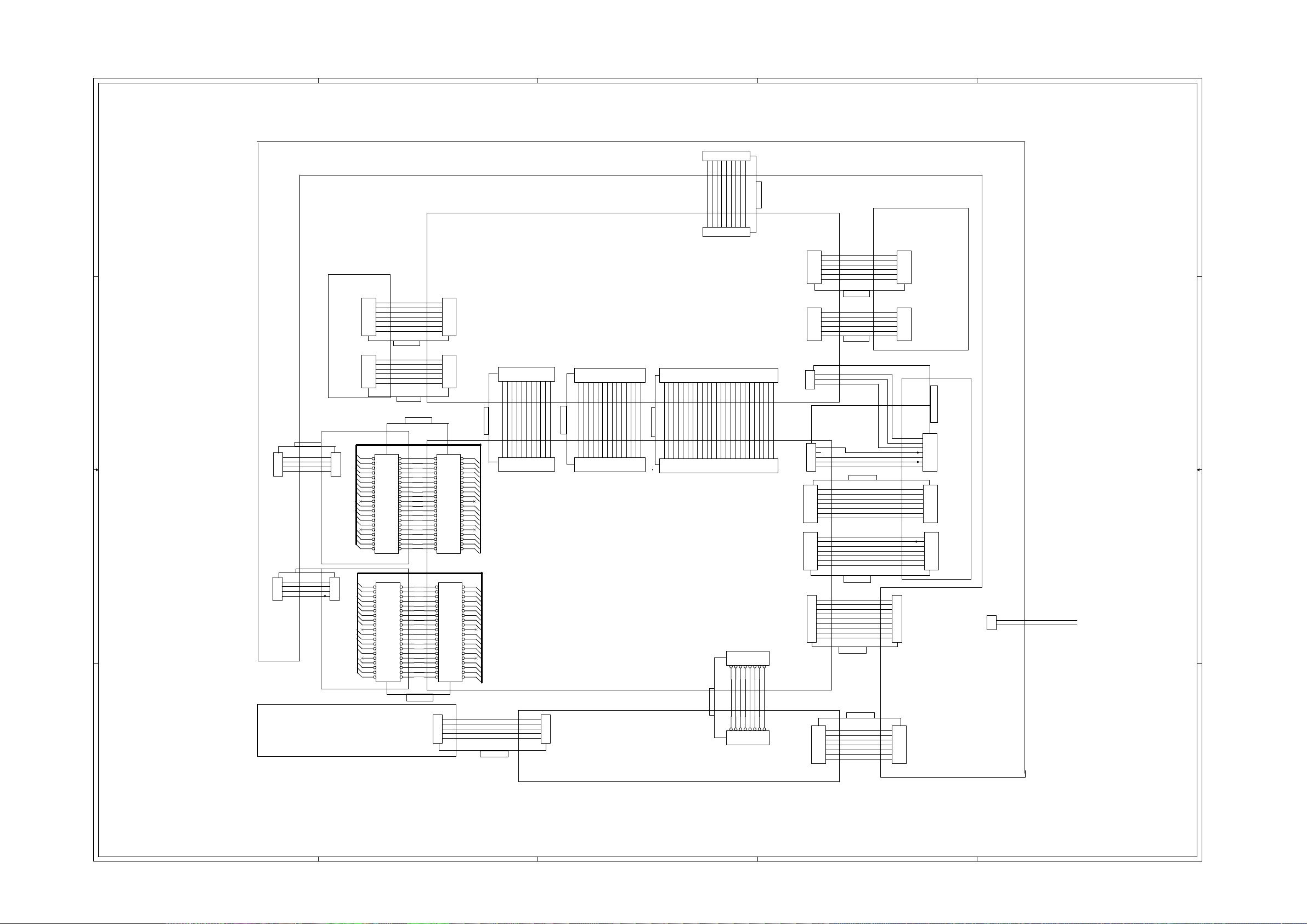
DVDR3435H/93 Block Diagram
D D
TUNER
AUDIO IN 1
AUDIO IN 2
AUDIO IN 3
AUDIO
SW
CS5340
AUDIO ADC
USB
1394
TUNER
C C
Y
PHY
1EEE1394
POWER
Pb
Pr
Y
C
CVBS
VIDEO
DECODER
DMN8652
Y
Pb
Pr
Y
C
CVBS
BUFFER
B B
7404
RW LOAD ATAPI
COAX
OPTICAL
BUFFER
AUDIO LCH
4558
AUDIO RCH
HDD 250G
CS4360
FLASH
SDRAM*1
SDRAM*2
AUDIO
DAC
4558
A A
FORNT
PANEL KEY
AUDIO SLCH
AUDIO SRCH
AUDIO SWCH
AUDIO CENCH
IR & VFD
BUFFER
5
4
3
2
1
A
5-3
5-3
B
C
D
E
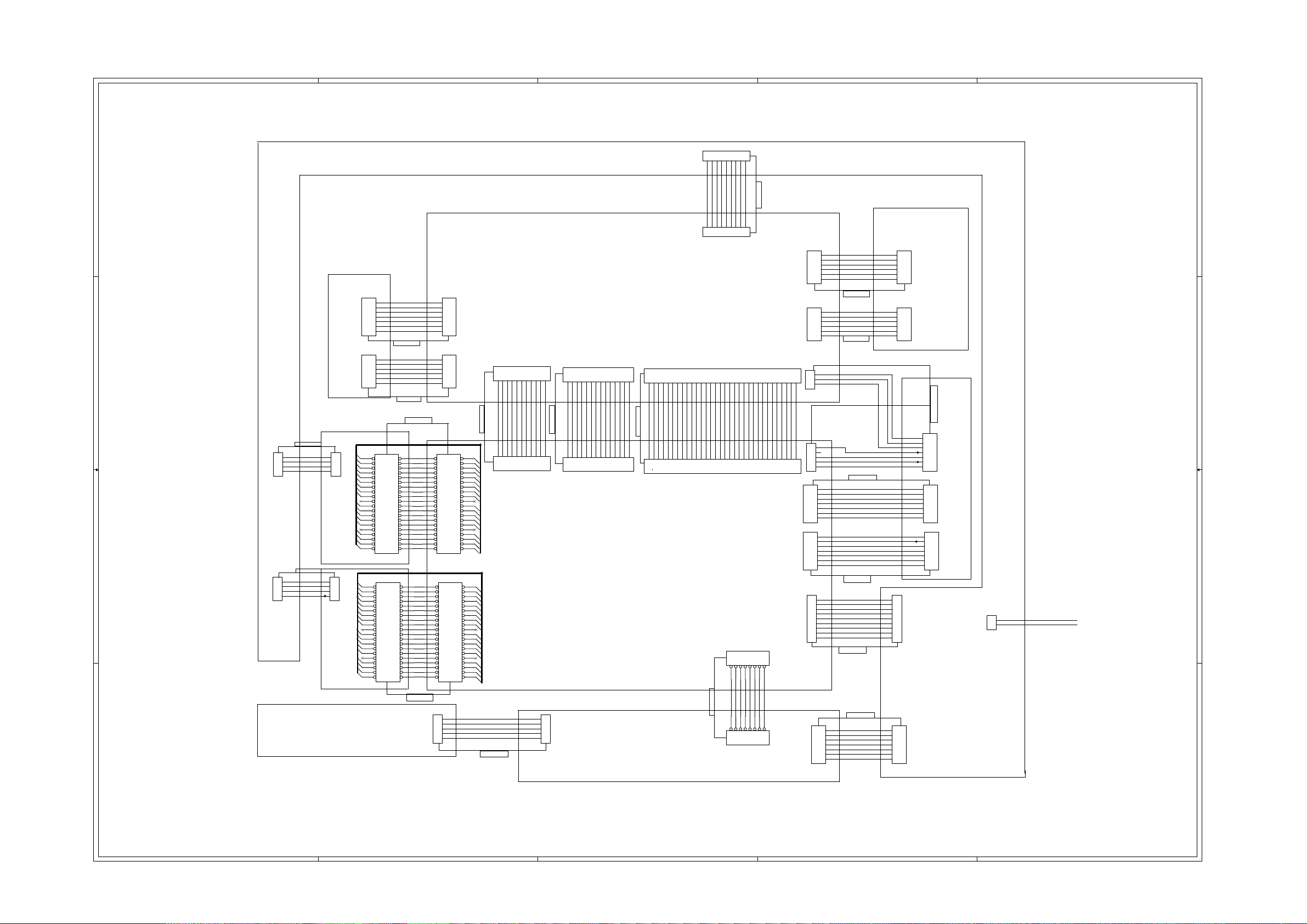
DVDR3425H/93 Wiring Diagram
CN7
123456789
POWER BOARD
4 4
CON9/2MM
+5V
32V
+5VSTB
GND
GND
XP2
123456789
CON9/2MM
2501 270mm
2518 270mm
PICH=2.0
CON7/2MM
7
6
5
4
3
2
1
XP5
CON6/2MM
6
5
4
3
2
1
XP4
J14
12
34
56
78
910
11 12
13 14
15 16
17 18
19 20
21 22
23 24
25 26
27 28
29 30
31 32
33 34
35 36
37 38
39 40
HEADER 20X2
J3
12
34
56
78
910
11 12
13 14
15 16
17 18
19 20
21 22
23 24
25 26
27 28
29 30
31 32
33 34
35 36
37 38
39 40
HEADER 20X2
J1
1
2
3
4
5
PW_SW
PW-SW1
LED1
GND
LED2
XP9
FMN11/1.0mm
2502 140mm
JP4
FMN11/1.0mm
2513 200mm
Pr/R_OUT
1234567891011
CVBS_OUT
GND
Y/G_OUT
GND
GND
Pb/B_OUT
123456789
GND
Y_OUT
GND
10
JP3
1
2
3
4
5
PICH=2.0
2503 150mm
C_OUT
11
AV BOARD
XP8
FMN14/1.0mm
12345678910111213
GND
Y/G_IN
R/Y_IN
R/C_IN
Pb/B_IN
Pr/R_IN
GND
GND
123456789
JP5
FMN14/1.0mm
GND
CVBS_IN
GND
GND
1011121314
GND
TV_CVBS_IN
MAIN BOARD
FRONT BOARD
XP3
FMN24/1.0mm
14
1234567891011121314151617181920212223
+3.3V
AO_MCLK
E5_SPI_MISO
GND
2504 80mm
AO_D0
AO_FSYNC
123456789
JP2
FMN24/1.0mm
AO_SCLK
GND
MUTE
E5_SPI_CLK
E5_SPI_CS2
E5_SPI_MOSI
101112131415161718192021222324
2512 150mm
RST_AUD
IDS_SDA
J4
PH8/2MM
JP2
PH8/2MM
CON7/2MM
JP1
CON6/2MM
OUTPUT BOARD
3 3
2505 380mm
+5V
CON3/2MM
CN6
1
2
3
4
GND
GND
+12V
1
2
3
4
HDD
HEADER 20X2
2 2
CON3/2MM
2519 380mm
+5V
CN6
1
2
3
4
GND
GNDGND
+12V
1
2
3
4
LOADER
7
6
5
4
3
2
1
6
5
4
3
2
1
JP2
HEADER 20X2
CVBS
C
Y
GND
R
G
B
2511 120mm
ROUT
GND
LOUT
VCC
GND
IEC_AUDIO
2506 80mm
12
34
56
78
910
1112
1314
1516
1718
1920
2122
2324
2526
2728
2930
3132
3334
3536
3738
3940
12
34
56
78
910
1112
1314
1516
1718
1920
2122
2324
2526
2728
2930
3132
3334
3536
3738
3940
SWITCH BOARD
1 1
2510 330mm
GND
+12V
GND
-12V
XP6
CON6/2MM
XP7
CON6/2MM
XP1
PH7/2MM
3
2
1
CON3
PICH=2.0
J2
J9
PH7/2MM
J1
CON9/2MM
1
2
3
4
5
1
2
3
4
5
6
7
8
9
JP1
PH7/2MM
24
AI_D0
IDS_SCL
AI_SCLK
TUN_DET
CH_SW
GND
AI_FSYNC
AI_MCLKO
GND
AO_IEC958
1234567
8
D_FM
R-M
RS_G
GND
D_T
S_G
IR
A_M
1234567
8
TV_SCL
6
TV_SDA
5
TV_V5
4
TV_V32
3
GND
2
VTUN_STB
1
2509 300mm
TV_AO
6
GND
5
TV_IF
4
TV_AFT
3
GND
2
TV_CVBSO
1
2508 300mm
AIN_R_F
GND
AIN_L_F
J10
7
6
5
4
3
2
1
7
6
5
4
3
2
1
F_CVBS
F_Y-IN
GND
F_C_IN
2514 350mm
CTPA+
CTPAGND
CTPB+
CTPBGND
GND
VCC
GND
BOMO
BOPO
GND
/OC
/EN
2515 380mm
GND
GND
+3.3V
+3.3V
+5V
+2.5V
+2.5V
GND
GND
2507 250mm
2516 125mm
+12V
7
GND
6
-24V
5
GND
4
VCC
3
F_C
2
P-C
1
CON6/2MM
6
5
4
3
2
1
CON2
CON6/2MM
6
5
4
3
2
1
CN7
1
2
3
4
5
6
7
8
9
CON9/2MM
CN1
7
6
5
4
3
2
1
PH7/2MM
CON1
TUNER BOARD
2517 280\300mm
J4
7
6
5
4
3
2
1
PH7/2MM
J8
7
6
5
4
3
2
1
PH7/2MM
JP2
7
6
5
4
3
2
1
PH7/2MM
INPUT BOARD
CON3
CN3
1
2
AC220V
AC220V
A
B
C
D
E
5-4
5-4
A
B
C
D
E
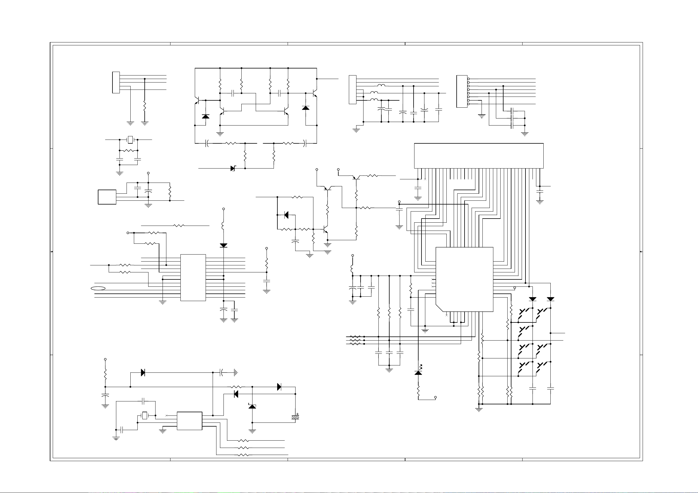
DVDR3435H/93 Wiring Diagram
CN7
123456789
POWER BOARD
4 4
CON7/2MM
JP1
CON6/2MM
OUTPUT BOARD
3 3
JP2
CVBS
7
C
6
Y
5
GND
4
R
3
G
2
B
1
3511 120mm
ROUT
6
GND
5
LOUT
4
VCC
3
GND
2
IEC_AUDIO
1
3506 80mm
CON7/2MM
7
6
5
4
3
2
1
XP5
CON6/2MM
6
5
4
3
2
1
XP4
XP9
FMN11/1.0mm
1234567891011
AV BOARD
XP8
FMN14/1.0mm
12345678910111213
14
XP3
FMN32/1.0mm
CON9/2MM
+5V
32V
+5VSTB
GND
GND
XP2
123456789
CON9/2MM
12345678910111213141516171819202122232425262728293031
3510 330mm
GND
+12V
GND
-12V
32
XP6
CON6/2MM
6
5
4
3
2
1
XP7
CON6/2MM
6
5
4
3
2
1
XP1
3
2
1
CON3
TV_SCL
TV_SDA
TV_V5
TV_V32
GND
VTUN_STB
3509 300mm
TV_AO
GND
TV_IF
TV_AFT
GND
TV_CVBSO
3508 300mm
AIN_R_F
GND
AIN_L_F
CON6/2MM
6
5
4
3
2
1
CON2
CON6/2MM
6
5
4
3
2
1
CON1
TUNER BOARD
3501 270mm
3505 380mm
+5V
CN6
1
2
3
4
CON3/2MM
2 2
CON3/2MM
3519 380mm
CN6
1
2
3
4
GND
GND
+12V
GND
GNDGND
+12V
1
2
3
4
HDD
+5V
1
2
3
4
LOADER
HEADER 20X2
HEADER 20X2
12
34
56
78
910
1112
1314
1516
1718
1920
2122
2324
2526
2728
2930
3132
3334
3536
3738
3940
12
34
56
78
910
1112
1314
1516
1718
1920
2122
2324
2526
2728
2930
3132
3334
3536
3738
3940
SWITCH BOARD
1 1
3518 270mm
PICH=2.0
J14
12
34
56
78
910
11 12
13 14
15 16
17 18
19 20
21 22
23 24
25 26
27 28
29 30
31 32
33 34
35 36
37 38
39 40
HEADER 20X2
J3
12
34
56
78
910
11 12
13 14
15 16
17 18
19 20
21 22
23 24
25 26
27 28
29 30
31 32
33 34
35 36
37 38
39 40
HEADER 20X2
J1
1
2
3
4
5
PW_SW
PW-SW1
LED1
GND
LED2
3502 140mm
Pr/R_OUT
JP4
FMN11/1.0mm
3513 200mm
GND
GND
Y/G_OUT
GND
Pb/B_OUT
123456789
3503 150mm
CVBS_OUT
C_OUT
GND
10
11
GND
Y/G_IN
GND
Pr/R_IN
Pb/B_IN
123456789
JP5
FMN14/1.0mm
GND
R/Y_IN
R/C_IN
GND
GND
Y_OUT
MAIN BOARD
JP3
1
2
3
4
5
PICH=2.0
FRONT BOARD
CVBS_IN
GND
GND
1011121314
TV_CVBS_IN
GND
3504 60mm
AO_D3
AO_D2
AO_D1
123456789
JP2
FMN32/1.0mm
E5_SPI_CS2
AO_FSYNC
+3.3V
AO_D0
AO_SCLK
AO_MCLK
GND
GND
GND
1011121314151617181920212223242526272829303132
E5_SPI_MOSI
E5_SPI_MISO
IDS_SDA
RST_AUD
E5_SPI_CLK
MUTE
J4
PH8/2MM
R-M
3512 150mm
JP2
PH8/2MM
AI_FSYNC
AI_D0
IDS_SCL
8
S_G
A_M
8
CH_SW
TUN_DET
GND
GND
CS_8775
CS_8776
AO_IEC958
VCR/TV
GND
J10
1
2
3
4
5
PICH=2.0
J2
PH7/2MM
7
6
5
4
3
2
1
J9
PH7/2MM
7
6
5
4
3
2
1
J1
CON9/2MM
1
2
3
4
5
6
7
8
9
1234567
RS_G
1234567
JP1
PH7/2MM
F_CVBS
F_Y-IN
GND
F_C_IN
3514 350mm
CTPA+
CTPAGND
CTPB+
CTPBGND
GND
VCC
GND
BOMO
BOPO
GND
/OC
/EN
3515 380mm
GND
GND
+3.3V
+3.3V
+5V
+2.5V
+2.5V
GND
GND
3507 250mm
3516 125mm
+12V
7
GND
6
-24V
5
GND
4
VCC
3
F_C
2
P-C
1
CN7
1
2
3
4
5
6
7
8
9
CON9/2MM
CN1
7
6
5
4
3
2
1
PH7/2MM
AI_SCLK
GND
AI_MCLKO
D_FM
D_T
IR
3517 280\300mm
J4
7
6
5
4
3
2
1
PH7/2MM
J8
7
6
5
4
3
2
1
PH7/2MM
JP2
7
6
5
4
3
2
1
PH7/2MM
INPUT BOARD
CN3
1
2
CON3
AC220V
AC220V
A
B
C
D
E
6-1 6-1
5
4
3
2
1
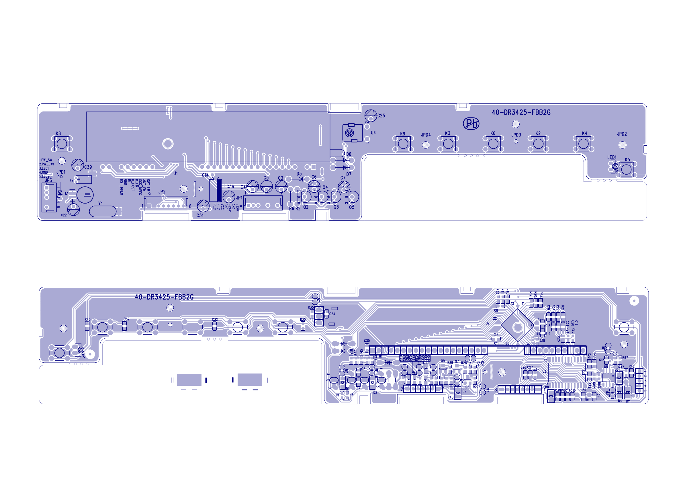
DVDR3425H/93, DVDR3435H/93 Front Board Electrical Diagram
TITLE: FB BOARD
J3
1
2
3
4
5
D D
PICH=2.0
TO SWITCH BOARD
Y1
22P
IR
10K(OPEN)
10K(OPEN)
3
2
1
VCC
R1
1M
R85
R86
12MHz
C24
0.1u
OSC_1
C9
U4
REM
VCC
POW_SW
IDC_SCL
FAN
IDC_SDA
INT_FP
GND
C C
B B
POW_SW
POW_SW1
LED1
LED2
R42
0(OPEN)
OSC_2
C10
22P
VCC
C25
+
47uF/16V
FAN FAN_CTL
R38
10K(OPEN)
R39
10K(OPEN)
P_CON
DATA ATN_FM
CS
Q2
2n222
1UF/50V
R35
4K7
IR
R16
10K
U3
1
P_CON
2
DATA
3
NC
4
5
6
7
8
9
10
11
12 13
OSC2
CS
OSC1
NC
RESET
VSS
VSS
CLK
SCL
D_FM
SDA
D_HOST
DATA_T
RST_TRST_M
PIC16C54S
C6
-24VV
RDY
ATN
VDD
VDD
SCK
1N4148/SMT
IR
680/DIP
D2
+
24
23
22
21
20
19
18
17
16
15
14
C51
47UF/16V
R2
RB751
D8
Q4
2n2222/DIP
R11
1
D5
5.6V/DIP
VCC
FB10
12
SCK_MPEG
RST_MPEG
+
C1
104
RDY_FM
OSC_1
OSC_2
RESET
D_FM
D_HOST
IR
100P
3.3k
C31
+
C7
+12V
Q3
2n2222/DIP
VCC
Q7
3906/SMT
R88
5.6K
VCC
R29
1K
Q9
3904/SMT
FB11
47uF/16V
R4
+F1
R13
680
+F2
P_CON
VCC
R5
3.3k
C2
104
Q5
2n2222/DIP
R14
680
D9 1N4148
R18
10K
C17
20p
R48
33K
R6
680/DIP
R12
R36
NC
+
C36
D1
1N4148/SMT
1
1UF/50V
R49
7.5K
100uF/16V
To Power Board
JP1
1
2
VCC1
3
4
5
6
7
PITCH=2.0
47uF/16V
Q8
3906/SMT
R28
4K7
C14
R24 100R
R25 100R
R26 100R
R27
330
R34
330
R37
1K
VCC
C15
0.1u
+
C16
0.1u
FB2
FB3
R21
10K
To Main Board
C34
100P
PITCH=2.0MM
8
7
6
5
4
3
2
1
JP2
C26 100p
C27 100p
C28 100p
FB1
+12V
C33
C3
+
100P
P_CON
FAN_CTL
VCC
-24VV
C35
100P
47uF/16V
C5
+
47uF/35V
C4
+
RDY_FM
ATN_FM
SCK_MPEG
D_FM
D_HOST
IR
RST_MPEG
U1
VFD Display
LED1
LED2
R22
10K
R23
10K
+F2
-24VV
C11
0.1u
F2F26G5G4G3G2G1GNCNCNCNCNCNCNCP1P2P3P4P5P6P7P8P9P10
NC
3534323130292827262524232221201918171615141312111098765432
33
C29
0.1u
2324252627282930313233
G6
R19
51K
C18
NC
CS
IDC_SCL
DATA
G5
34
G4
35
G3
36
G2
37
G1
38
VDD
39
LED4
40
LED3
41
LED2
42
LED1
43
GND
44
OSC
SW1
1234567891011
SW2
SEG13
SEG14
SEG15
SEG16
U2
PT6312
SW3
SW4
SDout
SDin
VEE
GND
SEG11
SEG12
SEG6/K6
SEG5/K5
SEG4/K4
SEG3/K3
SEG2/K2
SEG1/K1
SCLK
/CS
SEG9
SEG10
SEG8
SEG7
VDD
KEY4
KEY3
KEY1
KEY2
R20
2.2k
P11
P12
P13
P14
P15
P16NPF1
F1
1
+F1
C30
0.1u
22
21
20
19
18
17
16
VCC
15
14
13
12
R41
2.2k
R40
2.2k
D6
STOP
K2
K4
1N4148/SMT
D7
K3
OP/CL
PLAY/PAUSE
C1 D4
C2 D4
C3 D3
C4 D3
C5 D3
C6 D4
C7 D4
C9 D5
C10 D5
C11 C3
C12 A5
C13 A5
C14 B3
C15 B3
C16 B3
C17 B4
C18 B3
C19 B3
C20 B3
C21 B3
C22 B4
C24 C5
C25 C5
C26 D2
C27 D2
C28 D2
C29 C3
C30 C2
C31 B4
C32 A2
C33 D3
C34 D3
C35 D3
C36 C4
C39 A5
C50 A2
C51 B4
D1 D4
D2 D4
D3 B5
D4 A4
1N4148/SMT
POW_SW
POW_SW1
D5 C4
D6 B2
D7 B2
D8 C4
D9 C4
D10 A4
D11 A4
E1 A4
FB1 D3
FB2 D3
FB3 D3
FB10C4
FB11C3
JP1 D3
JP2 D2
J3 D5
K2 B2
K3 B2
K4 B2
K5 B2
K6 B2
K8 B2
K9 B2
LED1 B3
Q2 D5
Q3 D4
Q4 D4
Q5 D4
Q7 C3
Q8 C3
Q9 C3
R1 D5
R2 D4
R4 D4
R5 D4
R6 D4
R11 D4
R12 D4
R13 D4
R14 D4
R16 C5
R17 B2
R18 C4
R19 B3
R20 B2
R21 B3
R22 B3
R23 B3
R24 B3
R25 B3
R26 B3
R27 C3
R28 C3
R29 C3
R30 A2
R31 A2
R32 A2
R33 A2
R34 C3
R35 C5
R36 C4
R37 C3
R38 C5
R39 C5
R40 B2
R41 B2
R42 D5
R43 A3
R47 A4
R48 C4
R49 C4
R82 A4
R83 A4
R84 A4
R85 C5
R86 C5
R87 B5
R88 C4
U1 D3
U2 C3
U3 C5
U4 C5
U5 A5
X13 A2
Y1 D5
Y2 A5
VCC1
8
7
6
C22
22UF/16V
+
R47 470
D4 RB751
D10
R83 47
R82 47
R84 47
4
12
3.3V/0.5W
1 2
D11 RB751
1 2
IDC_SCL
IDC_SDA
INT_FP
E1
BATTERY3V
3
D3 RB751
C13
12.5P
1 2
C12
12.5P
Y2
32.768K
R87
1K
C39
+
47UF/16V
A A
5
IDC Slave Addr: D0H/D1H
VCC1
U5
1
INT1
2
3
4 5
VCC1
XIN
SCL
XOUT
SDA
GND RESET
HT1381
C19
47P
C20
47P
C21
47P
330
LED1
SACD
R43
VCC
R17
2.2k
R32
R30
10K
2
R31
10K
10K
PREVIOUS
R33
10K
K5
NEXT
K6
C32
NC
K8
CH+
CH-
K9
C50
NC
1
6-2
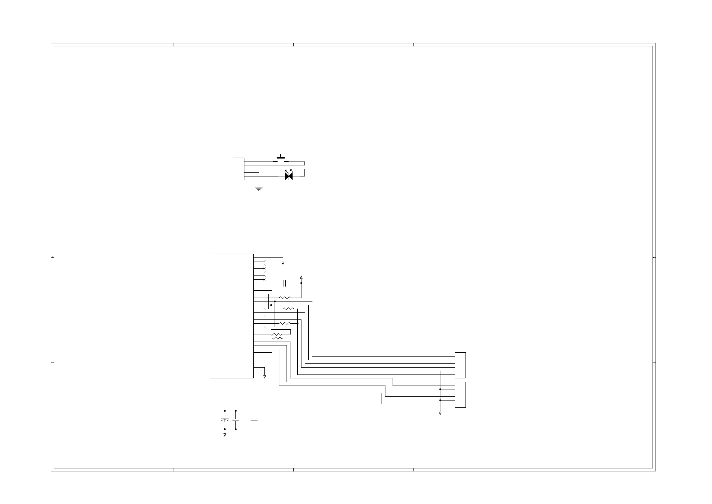
Front Board Print-layout (Top Side) for DVDR3425H/93, DVDR3435H/93
6-2
Front Board Print-layout (Bottom Side) for DVDR3425H/93, DVDR3435H/93
6-3
6-3
5
4
3
2
1
DVDR3425H/93, DVDR3435H/93 Switch Board & Tuner Board Electrical Diagram
D D
C C
TITLE:SW BOARD
J1
2MM
1
2
3
4
5
POWER_SWITCH
POWER_LED
SWITCH BOARD
K1 POWER
POW SW
POW SW1
LED1
LED2
D3
CON2 D4
X13 A2
D3 D4
K1 D4
TITLE:TUNER BOARD
IDC Slave Addr: 0xC0/C1
TUN1
B B
A A
C2
22UF/50V
PAL:
GND
AUDIO-IN:NC:NC
CH_SW:NC:NC
+B/MB:NC:NC
CONTROL:NC:NC
VIDEO_IN:NC:NC
NC:RF_AGC:RF_AGC
NC:NC:NC
NC:AS:AS
SCL:SCL:SCL
SDA:SDA:SDA
AFT_OUT:NC:NC
A_OUT:+B:+B
SIF_OUT:NC:NC
TU:TU:TU
V_OUT:IF_AGC:IF_AGC
NC:SIF_OUT:SIF_OUT
NC:AFT_OUT:AFT_OUT
+32
GND_TUN
NC:NC:NC
NC:SW1:SDA
NC:SW2:SCL
NC:A_OUT:A_OUT
NC:V_OUT:V_OUT
Chassis_GND
TMDZ9-731A
12
C3
+
0.1UF
NC
26
1
2
3
4
5
6
8
9
10
11
12
13
14
15
16
17
18
19
20
21
22
23
24
25
GND_TUN
12
C4
0.1UF
GND_TUN
C1 0.1UF
1 2
R1 0
R5 0
R3 0
1 2
1 2
R4 0
R2 0
GND_TUN
12
12
12
SCL
SDA
+B
+32
VTUN_STB
TUN_AO
IF_OUT
AFT_OUT
CVBS_OUT
GND_TUN
FMN14/1.0mm
6
5
4
3
2
1
6
5
4
3
2
1
FMN14/1.0mm
C1 D4
J9
C3 B4
C4 B4
R1 C4
R2 C4
R3 C4
J7
R4 C4
R5 C4
C2 B5
J7 C3
J9 C3
TUN1 D5
U5 A2
5
4
3
2
1
6-4
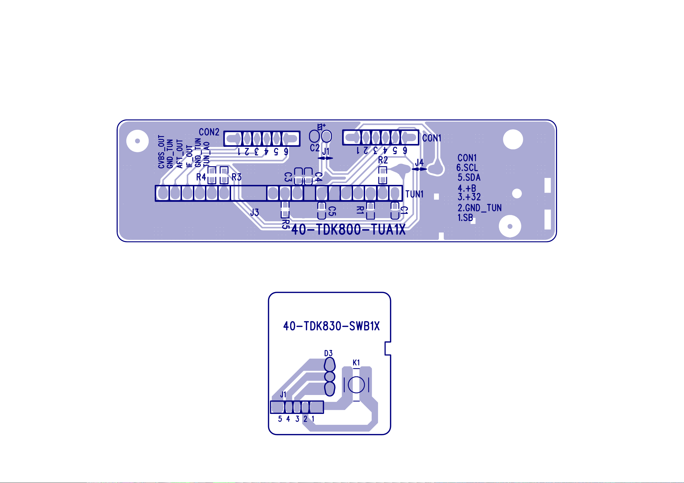
Tuner Board Print-layout (Bottom Side) for DVDR3425H/93, DVDR3435H/93
6-4
Switch Board Print-layout (Bottom Side) for DVDR3425H/93, DVDR3435H/93
 Loading...