

Page 1

VCR Module
HK100ED
2422 549 01124
Service
Service
Service
Service Manual
Contents
Chapter
Sec. 1: Schematic Diagrams and CBA's
Exploded Views
Mechanical and Electrical Parts Lists
Sec. 2: Standard Maintenance
Mechanism Alignment Procedures
Disassembly / Assembly of Mechanism
Deck Exploded Views
Deck Parts List
c Copyright 2006 Philips Consumer Electronics B.V. Eindhoven, The Netherlands.
All rights reserved. No part of this publication may be reproduced, stored in a retrieval
system or transmitted, in any form or by any means, electronic, mechanical, photocopying,
or otherwise without the prior permission of Philips.
Published by FU-KC 0623 Service AV Systems Printed in Netherlands Subjection to modification EN 3139 785 32220
Version 1.0
Page 2

MAIN SECTION
VCR Module
Sec. 1: Main Section
I Schematic Diagrams and CBA’s
I Exploded Views
I Mechanical and Electrical Parts List
TABLE OF CONTENTS
STANDARD NOTES FOR SERVICING . . . . . . . . . . . . . . . . . . . . . . . . . . . . . . . . . . . . . . . . . . . . . . . . . . . . . . 1-1-1
SIGNAL NAME ABBREVIATIONS. . . . . . . . . . . . . . . . . . . . . . . . . . . . . . . . . . . . . . . . . . . . . . . . . . . . . . . . . . 1-2-1
ELECTRICAL ADJUSTMENT INSTRUCTIONS . . . . . . . . . . . . . . . . . . . . . . . . . . . . . . . . . . . . . . . . . . . . . . . 1-3-1
BLOCK DIAGRAMS. . . . . . . . . . . . . . . . . . . . . . . . . . . . . . . . . . . . . . . . . . . . . . . . . . . . . . . . . . . . . . . . . . . . . 1-4-1
SCHEMATIC DIAGRAMS / CBA’S AND TEST POINTS . . . . . . . . . . . . . . . . . . . . . . . . . . . . . . . . . . . . . . . . . 1-5-1
WAVEFORMS . . . . . . . . . . . . . . . . . . . . . . . . . . . . . . . . . . . . . . . . . . . . . . . . . . . . . . . . . . . . . . . . . . . . . . . . . 1-6-1
WIRING DIAGRAM . . . . . . . . . . . . . . . . . . . . . . . . . . . . . . . . . . . . . . . . . . . . . . . . . . . . . . . . . . . . . . . . . . . . . 1-7-1
IC PIN FUNCTION DESCRIPTIONS. . . . . . . . . . . . . . . . . . . . . . . . . . . . . . . . . . . . . . . . . . . . . . . . . . . . . . . . 1-8-1
LEAD IDENTIFICATIONS . . . . . . . . . . . . . . . . . . . . . . . . . . . . . . . . . . . . . . . . . . . . . . . . . . . . . . . . . . . . . . . . 1-9-1
ELECTRICAL PARTS LIST . . . . . . . . . . . . . . . . . . . . . . . . . . . . . . . . . . . . . . . . . . . . . . . . . . . . . . . . . . . . . . 1-10-1
EXPLODED VIEWS. . . . . . . . . . . . . . . . . . . . . . . . . . . . . . . . . . . . . . . . . . . . . . . . . . . . . . . . . . . . . . . . . . . . 1-11-1
MECHANICAL PARTS LIST . . . . . . . . . . . . . . . . . . . . . . . . . . . . . . . . . . . . . . . . . . . . . . . . . . . . . . . . . . . . . 1-12-1
Page 3

STANDARD NOTES FOR SERVICING
Circuit Board Indications
1. The output pin of the 3 pin Regulator ICs is
indicated as shown.
Top View
Out
2. For other ICs, pin 1 and every fifth pin are
indicated as shown.
Pin 1
3. The 1st pin of every male connector is indicated as
shown.
Pin 1
Input
In
Bottom View
5
10
Pb (Lead) Free Solder
When soldering, be sure to use the Pb free solder.
Information about lead-free soldering
Philips CE is producing lead-free sets from 1.1.2005
onwards.
IDENTIFICATION
Regardless of special logo (not always
indicated)
One must treat all sets from
onwards, according to the next rule:
Serial Number gives a 9-digit. Digit 2&3 shows the
WEEK, and digit 4 shows the YEAR.
So from onwards=from 1 Jan 2005 onwards
Important note: In fact also products of year 2004
must be treated in this way as long as you avoid
mixing solder-alloys (leaded/ lead- free) . So bes t to
always use SAC305 and the higher temperatures
belong to this.
Due to lead-free technology some rules have to be
respected by the workshop during a repair:
• Use only lead-free solder alloy Philips SAC305 with
order code 0622 149 00106. If lead-free solderpaste is required, please contact the manufacturer
of your solder-equipment. In general use of solderpaste within workshops should be avoided because
paste is not easy to store and to handle.
• Use only adequate solder tools applicable for leadfree solder alloy. The solder tool must be able
• To reach at least a solder-temperature of 400°C,
• To stabilize the adjusted temperature at the solder-
• To exchange solder-tips for different applications.
• Adjust your solder tool so that a temperature around
360°C
solder joint. Heating-time of the solder-joint should
not exceed ~ 4 sec. Avoid temperatures above
400°C otherwise wear-out of tips will rise drastically
and flux-fluid will be destroyed. To avoid wear-out of
tips switch off un-used equipment, or reduce heat.
• Mix of lead-free solder alloy / parts with leaded
solder alloy / parts is possible but PHILIPS
recommends strongly to avoid mixed solder alloy
types (leaded and lead-free).
If one cannot avoid or does not know whether
product is lead-free, clean carefully the solder-joint
from old solder alloy and re-solder with new solder
alloy (SAC305).
• Use only original spare-parts listed in the ServiceManuals. Not listed standard-material (commodities)
has to be purchased at external companies.
015
tip
- 380°C is reached and stabilized at the
1 Jan 2005
1-1-1 HK100_SN
Page 4
• Special information for BGA-ICs:
- always use the 12nc-recognizable soldering
temperature profile of the specific BGA (for desoldering always use the lead-free temperature
profile, in case of doubt)
- lead free BGA-ICs will be delivered in so-called
'dry-packaging' (sealed pack including a silica gel
pack) to protect the IC against moisture. After
opening, dependent of MSL-level seen on indicatorlabel in the bag, the BGA-IC possibly still has to be
baked dry. (MSL=Moisture Sensitivity Level). This
will be communicated via AYS-website.
Do not re-use BGAs at all.
• For sets produced before 1.1.2005 (except products
of 2004), containing leaded solder-alloy and
components, all needed spare-parts will be available
till the end of the service-period. For repair of such
sets nothing changes.
• On our website
www.atyourservice.ce.Philips.com
information to:
• BGA-de-/soldering (+ baking instructions)
• Heating-profiles of BGAs and other ICs used in
Philips-sets
You will find this and more technical information within
the “magazine”, chapter “workshop news”.
For additional questions please contact your local
repair-helpdesk.
you find more
How to Remove / Install Flat Pack-IC
1. Removal
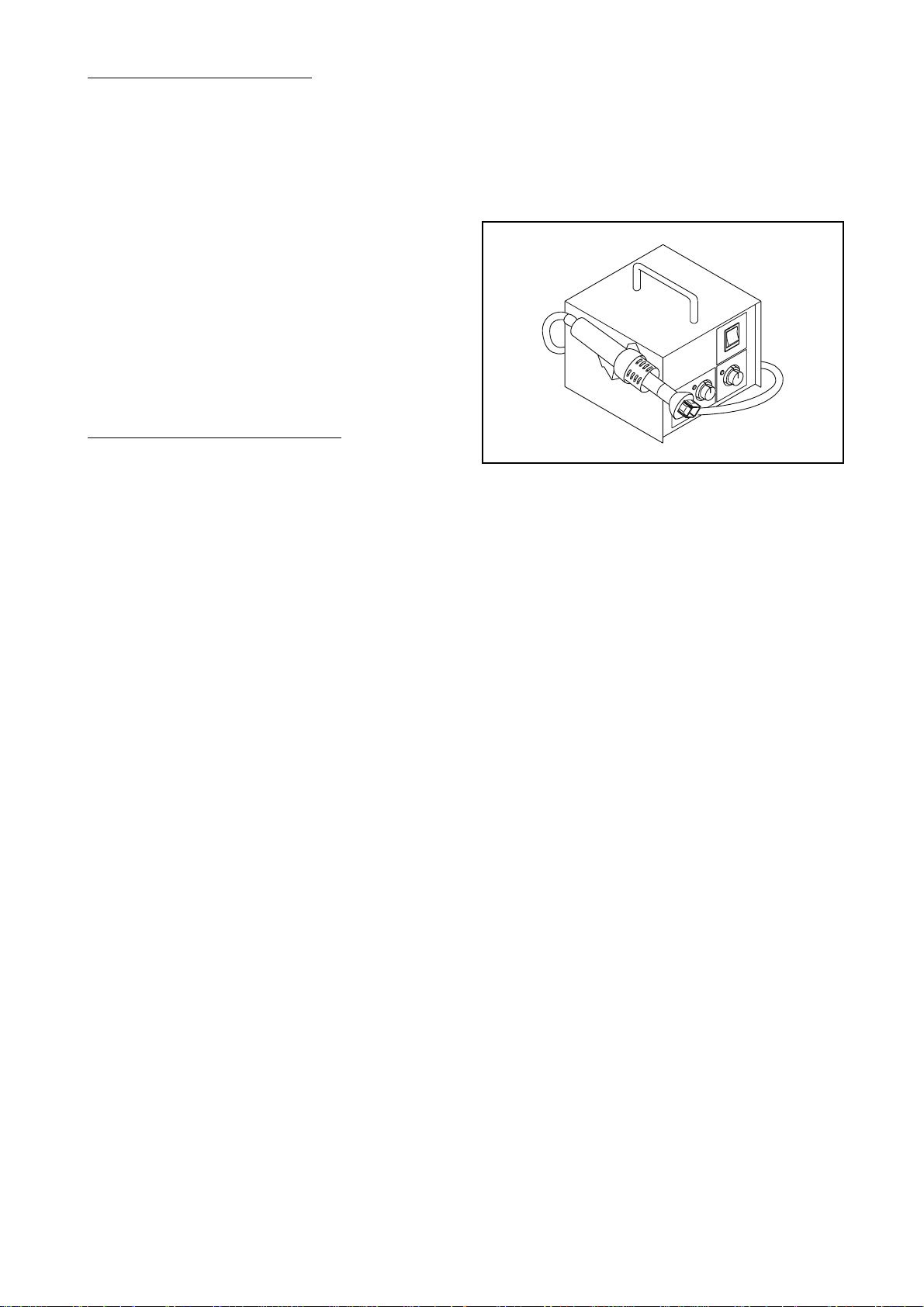
With Hot-Air Flat Pack-IC Desoldering Machine:
1. Prepare the hot-air flat pack-IC desoldering
machine, then apply hot air to the Flat Pack-IC
(about 5 to 6 seconds). (Fig. S-1-1)
Fig. S-1-1
2. Remove the flat pack-IC with tweezers while
applying the hot air.
3. Bottom of the flat pack-IC is fixed with glue to the
CBA; when removing entire flat pack-IC, first apply
soldering iron to center of the flat pack-IC and heat
up. Then remove (glue will be melted). (Fig. S-1-6)
4. Release the flat pack-IC from the CBA using
tweezers. (Fig. S-1-6)
CAUTION:
1. The Flat Pack-IC shape may differ by models. Use
an appropriate hot-air flat pack-IC desoldering
machine, whose shape matches that of the Flat
Pack-IC.
2. Do not supply hot air to the chip parts around the
flat pack-IC for over 6 seconds because damage
to the chip parts may occur. Put masking tape
around the flat pack-IC to protect other parts from
damage. (Fig. S-1-2)
1-1-2 HK100_SN
Page 5
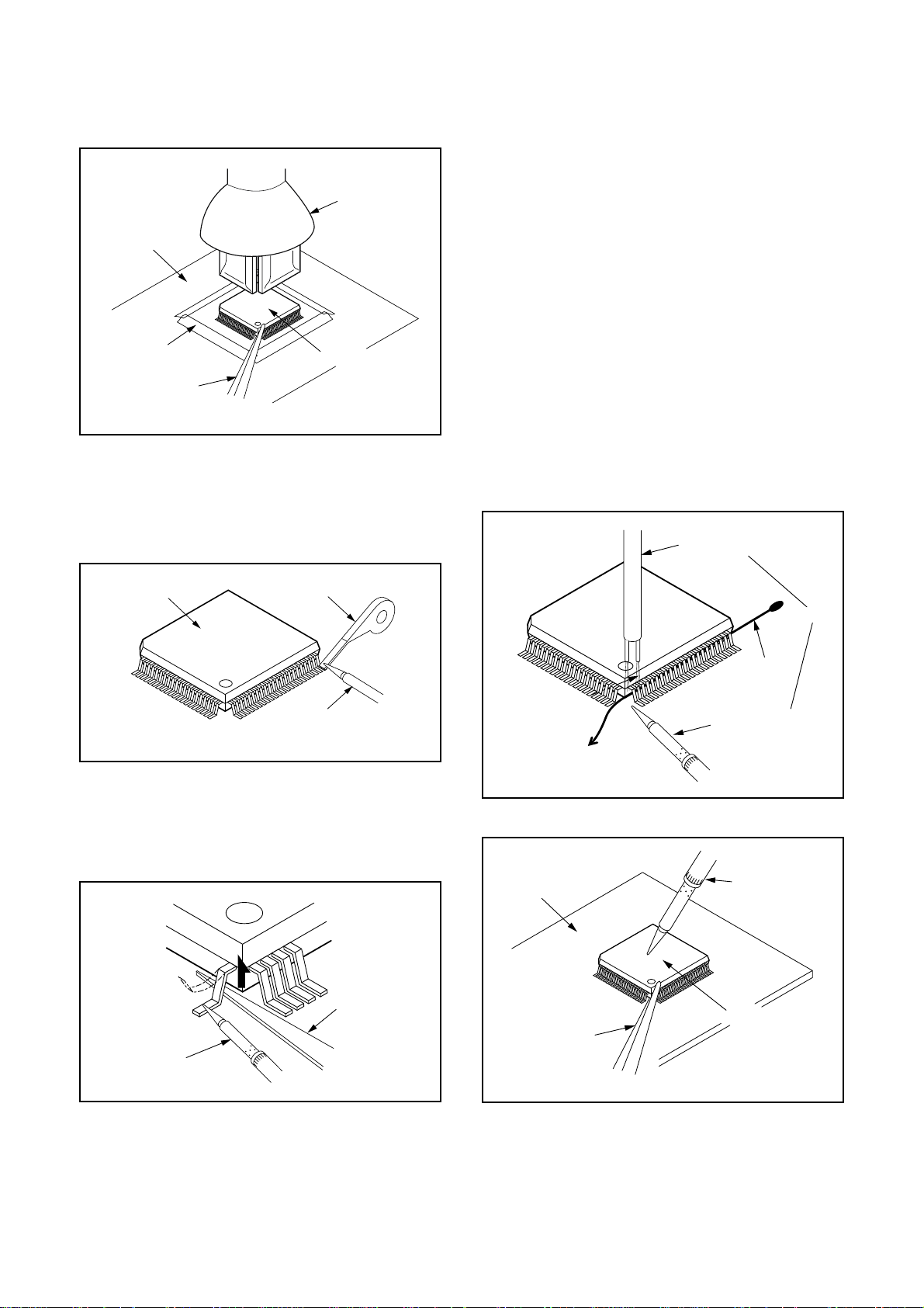
3. The flat pack-IC on the CBA is affixed with glue, so
be careful not to break or damage the foil of each
pin or the solder lands under the IC when
removing it.
Hot-air
Flat Pack-IC
Desoldering
CBA
Masking
Tape
Machine
Flat Pack-IC
Tweezers
Fig. S-1-2
With Soldering Iron:
1. Using desoldering braid, remove the solder from
all pins of the flat pack-IC. When you use solder
flux which is applied to all pins of the flat pack-IC,
you can remove it easily. (Fig. S-1-3)
With Iron Wire:
1. Using desoldering braid, remove the solder from
all pins of the flat pack-IC. When you use solder
flux which is applied to all pins of the flat pack-IC,
you can remove it easily. (Fig. S-1-3)
2. Affix the wire to a workbench or solid mounting
point, as shown in Fig. S-1-5.
3. While heating the pins using a fine tip soldering
iron or hot air blower, pull up the wire as the solder
melts so as to lift the IC leads from the CBA
contact pads as shown in Fig. S-1-5.
4. Bottom of the flat pack-IC is fixed with glue to the
CBA; when removing entire flat pack-IC, first apply
soldering iron to center of the flat pack-IC and heat
up. Then remove (glue will be melted). (Fig. S-1-6)
5. Release the flat pack-IC from the CBA using
tweezers. (Fig. S-1-6)
Note: When using a soldering iron, care must be
taken to ensure that the flat pack-IC is not
being held by glue. When the flat pack-IC is
removed from the CBA, handle it gently
because it may be damaged if force is applied.
Hot Air Blower
Flat Pack-IC
Desoldering Braid
Soldering Iron
Fig. S-1-3
2. Lift each lead of the flat pack-IC upward one by
one, using a sharp pin or wire to which solder will
not adhere (iron wire). When heating the pins, use
a fine tip soldering iron or a hot air desoldering
machine. (Fig. S-1-4)
Sharp
Pin
Fine Tip
Soldering Iron
Fig. S-1-4
To Solid
Mounting Point
CBA
Tweezers
or
Iron Wire
Soldering Iron
Fig. S-1-5
Fine Tip
Soldering Iron
Flat Pack-IC
Fig. S-1-6
3. Bottom of the flat pack-IC is fixed with glue to the
CBA; when removing entire flat pack-IC, first apply
soldering iron to center of the flat pack-IC and heat
up. Then remove (glue will be melted). (Fig. S-1-6)
4. Release the flat pack-IC from the CBA using
tweezers. (Fig. S-1-6)
1-1-3 HK100_SN
Page 6

2. Installation
1. Using desoldering braid, remove the solder from
the foil of each pin of the flat pack-IC on the CBA
so you can install a replacement flat pack-IC more
easily.
2. The “●” mark on the flat pack-IC indicates pin 1.
(See Fig. S-1-7.) Be sure this mark matches the 1
on the PCB when positioning for installation. Then
presolder the four corners of the flat pack-IC. (See
Fig. S-1-8.)
3. Solder all pins of the flat pack-IC. Be sure that
none of the pins have solder bridges.
Example :
Pin 1 of the Flat Pack-IC
is indicated by a " " mark.
Fig. S-1-7
Instructions for Handling Semiconductors
Electrostatic breakdown of the semi-cond uc tors may
occur due to a potential difference caused by
electrostatic charge during unpacking or repair work.
1. Ground for Human Body
Be sure to wear a grounding band (1 MΩ) that is
properly grounded to remove any static electricity that
may be charged on the body.
2. Ground for Workbench
Be sure to place a conductive sheet or copper plate
with proper grounding (1 MΩ) on the workbench or
other surface, where the semi-conductors are to be
placed. Because the static electricity charge on
clothing will not escape through the body grounding
band, be careful to avoid contacting semi-conductors
with your clothing.
<Incorrect>
CBA
Presolder
Flat Pack-IC
Fig. S-1-8
<Correct>
1MΩ
CBA
Grounding Band
1MΩ
CBA
Conductive Sheet or
Copper Plate
1-1-4 HK100_SN
Page 7
SIGNAL NAME ABBREVIATIONS
Signal Name Function
4.43MHz 4.43MHz clock
A-COM Audio Head Common
A-MODE Hi-Fi Tape Detection Signal
AE-H Audio Erase Head
AE-H/FE-H Audio Erase Head
AL+12V
AL+20V/+12V
AL+5V
AMPC CTL AMP Connected Terminal
AMPVcc AMPVcc
AMPVREF IN V-Ref for CTL AMP
AMPVREF OUT V-Ref for CTL AMP
AUDIO-MUTE-H
AUDIO-PB/REC
AUDIO(L)-IN L-ch Audio Input
AUDIO(L)-OUT L-ch Audio Output
AUDIO(R)-IN R-ch Audio Input
AUDIO(R)-OUT R-ch Audio Output
AVcc
CC Terminal
C CTL AMP Capacit or
C-CONT Capstan Motor Control Signal
C-F/R
C-FG
C-POW-SW Capstan Power Switching Pulse
C-ROTA
C-SYNC Composite Synchronized Pulse
CLKSEL Clock Select
CTL To Monitor for CTL AMP Output
CTL (+)
CTL (-)
D-CONT Drum Motor Control Signal
Always +12V with AC Plug
Connected
Always +20V/+12V with AC Plug
Connected
Always +5V with AC Plug
Connected
Audio Mute Control Signal
(Mute=“H”)
Normal Audio Play Back/Record
Signal
A/D Converter Power Input/
Standard Voltage Input
Capstan Motor FWD/REV
Control Signal (FWD=”L”/
REV=”H”)
Capstan Motor Rotation
Detection Pulse
Color Phase Rotary Changeover
SIgnal
Playback/Record Control Signal
(+)
Playback/Record Control Signal
(-)
Signal Name Function
D-PFG Drum Motor Pulse Generator
D-REC-H Delayed Record Signal
D-V-SYNC Dummy V-sync Output
END-S Tape End Position Detect Signal
FE-H Full Erase Head
FE-H-GND Ground for Full Erase Head
FSC-IN
[4.43MHz]
GND Ground
H-A-COMP Head Amp Comparator Signal
H-A-SW
Hi-Fi-AUDIO(L) Hi-Fi Audio L Head
Hi-Fi-AUDIO(R) Hi-Fi Audio R Head
Hi-Fi-COM Hi-Fi Audio Head Common
Hi-Fi-H-SW
HLF LPF Connected Terminal (Slicer)
IIC-BUS SCL
IIC-BUS SDA
KEY-1 Key Scan Input Signal 1
KEY-2 Key Scan Input Signal 2
LD-SW
LM-FWD/REV Loading Motor Control Signal
N-A-PB Normal Audio Playback
N-A-REC Normal Audio Recording
OSCin Clock Input for letter size
OSCout Clock Output for letter size
OSD-V-IN OSD Video Signal Input
OSD-V-OUT OSD Video Signal Output
OSDVcc OSDVcc
OSDVss OSD Ground
P-ON+5V +5V at Power-On Signal
P-ON+9V +9V at Power-On Signal
P-ON-L Power On Signal at Low
PB-H-OUT Playback control/Signal (PB=“H”)
PG-DELAY
POW-SAF
4.43MHz Clock Input
Video Head Amp Switching
Pulse
Hi-Fi Audio Head Switching
Pulse
2
C BUS Control Clock
I
2
I
C BUS Control Data
Deck Mode Position Detector
Signal
Video Head Switching Pulse
Signal Adjusted Voltage
P-ON Power Detection Input
Signal
1-2-1 HK100SNA
Page 8

Signal Name Function
REC-SAF-SW
REMOTE Remote Control Sensor
RESET System Reset Signal (Reset=“L”)
RF-SW Video Head Switching Pulse
S-CLOCK Serial clock
S-CS Chip Select Signal
S-DATA-IN Serial Data Input
S-DATA-OUT Serial Data Output
S-REEL Supply Reel Rotation Signal
Recording Safety SW Detect
(With Record tab=“L”/With out
Record tab=“H”)
SECAM-C-IN
SECAM-FM-
OUT
SECAM-H SECAM Mode at High
ST-S
T-REEL Take Up Reel Rotation Signal
TRICK-H
V-ENV
Vcc Vcc
VG+18V
VIDEO Video Signal
VIDEO(L)-1/2 Video L Head 1/2
VIDEO(R)-1/2 Video R Head 1/2
VIDEO-COM Video Head Common
SECAM CHROMA Signal from
PAL/SECAM DETECTOR
PB video Signal to PAL/SECAM
DETECTOR
Tape Start Position Detector
Signal
Trick Play Control Signal
(Trick=“H”)
Video Envelope Comparator
Signal
Always +18V with AC Plug
Connected
VIDEO-IN Video Signal Input
VIDEO-OUT Video Signal Output
Vss Vss(GND)
X-IN Main Clock Input
X-OUT Main Clock Input
1-2-2 HK100SNA
Page 9
ELECTRICAL ADJUSTMENT INSTRUCTIONS
General Note: "CBA" is an abbreviation for
"Circuit Board Assembly."
NOTE:
1.Electri cal adjustm ents are re quired after re placing
circuit components and certain mechanical par ts.
It is impor tant to do these adjustments only after
all repairs and replacements have been completed. Also, do not attempt these adjustments
unless the proper equipment is available.
2.To perfor m these alignment / confirmation procedures, make sure that the tracking control is set in
the center position : Press either "PR -5??" or "PR +"
button on the remote control unit first, then the "B"
button (Front Panel only).
Te st Equipment Required
1.Oscilloscope: Dual-trace with 10:1 probe,
V-Range: 0.001~50V/Div.,
F-Range: DC~AC-20MHz
2.Alignment Tape (9965 000 14514)
Head Switching Position Adjustment
Purpose:
To determ ine the Head Switching position during
playback.
Symptom of Misadjustment:
May cause Head Switch ing noise or vertical jit ter
in the picture.
Test point Adj.Point Mode Input
J909(V-OUT)
TP504(RF-SW)
GND
Tape
9965 000 14514 Oscilloscope
Connections of Measurement Equipment
Main CBA
TP504
VR501
(Switching Point)
(MAIN CBA)
Measurement
Equipment
J909
GND
PLAY
(SP)
6.5H±1H
(416µs±64µs)
Oscilloscope
-----
Spec.
CH1 CH2
Trig. (+)
Figure 1
EXT. Syncronize Trigger Point
CH1
CH2
Reference Notes:
Playback the Alignment tape and adjust VR501 so that
the V-sync front edg e of the CH1 video out put waveform is at the 6.5H±1H (416µs±64µs) delayed position
from the rising edge o f the CH2 head switching pulse
waveform.
1.0H
6.5H+/-1H (416µs+/-64µs)
Switching Pulse
0.5H
V-Sync
1-3-1 HK100EA
Page 10

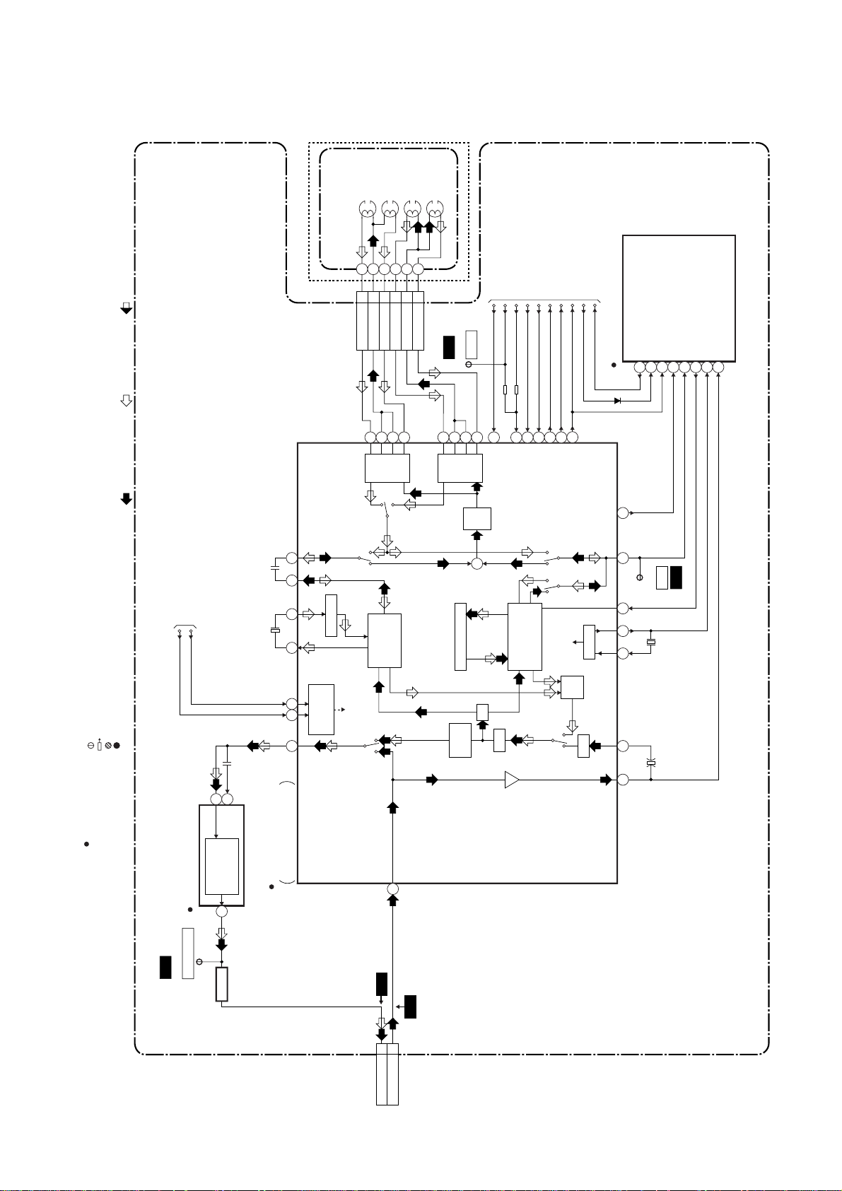
BLOCK DIAGRAMS
Servo / System Control Block Diagram
AL+20V/+12V
AL+5V
RESET
1 VG+18V
CN252
VG+18V
3
4 AL+12V
6 AL+12V
8 AL+5V
Q151
+9V REG.
AL+5V
AL+12V
P-ON+9V
AL+20V/+12V
10 C-POW-SW
Q153
P-ON+5V
CN653
TP505 SENS-INH
1 S-CLOCK
3 S-DATA-IN
7 S-CS
8 RESET
2 REMOTE
1 KEY-1
5 S-DATA-OUT
CN505
WF8WF9WF10WF11
Q515
Q152
SDA
SCL
IC502 (MEMORY)
5
6
TO AUDIO
BLOCK DIAGRAM
IIC-BUS SCL
IIC-BUS SDA
AUDIO-MUTE-H
TO Hi-Fi AUDIO
BLOCK DIAGRAM
A-MODE
Hi-Fi-H-SW
IIC-BUS SCL
IIC-BUS SDA
AUDIO-MUTE-H
RF-SW
D-REC-H
IIC-BUS SCL
IIC-BUS SDA
C-ROTA
D-V-SYNC
TO VIDEO
BLOCK DIAGRAM
V-ENV
H-A-SW
C-SYNC
TRICK-H
H-A-COMP
SECAM-H
8
7
14
KEY- 1
:INDICATES A TEST POINT WITH A JUMPER WIRE ACROSS A HOLE IN THE PCB.
:USED TO INDICATE A TEST POINT WITH A COMPONENT LEAD ON FOIL SIDE.
:USED TO INDICATE A TEST POINT WITH NO TEST PIN.
:USED TO INDICATE A TEST POINT WITH A TEST PIN.
TEST POINT INFORMATION
“ “ = SMD
NOTE FOR WIRE CONNECTORS:
1. PREFIX SYMBOL "CN" MEANS CONNECTOR.
(CAN DISCONNECT AND RECONNECT.)
2. PREFIX SYMBOL "CL" MEANS WIRE-SOLDER
HOLES OF THE PCB.
KEY- 2
REMOTE
IC501
(SERVO/SYSTEM CONTROL)
AL+5V
D555
S-LED
SW507
(WIRE IS SOLDERED DIRECTLY.)
LD-SW
MAIN CBA
CTL(+)
LD-SW
9
95
AL+5V
CN504
5 CTL(+)
67
66
S-CLOCK
S-DATA-IN
CTL(-)
94
6 CTL(-)
65
64
S-CS
S-DATA-OUT
34
RESET
END-S
ST-S
10480
60
C-POW-SW
T-REEL
S-REEL
79
END-S
TP502
PS502
Q506
S-REEL
T-REEL
75
P-ON-L
CTL
97
CTL
TP503
AL+5V
PG-DELAY
2
VR501
SW-POINT
83
AUDIO-MUTE-H
REC-SAF-SW
31
SW506
AL+5V
REC-SAFETY
CAPSTAN MOTOR
P-ON+5V
AL+20V/+12V
CN502
AL+20V/+12V
1
2 P-ON+5V
33
71
72
19
32
A-MODE
Hi-Fi-H-SW
C-FG
C-F/R
8778768177
C-F/R5C-CONT6GND7LM-FWD/REV
3 C-FG
4
IIC-BUS SCL
IIC-BUS SDA
C-CONT
LM-
MOTOR
DRIVE
CAPSTAN
D-REC-H
FWD/REV
D-CONT
D-CONT9D-PFG10GND11AL+12V
8
CIRCUIT
MOTOR
15
18
RF-SW
C-ROTA
D-PFG
90
M
17
16
13
H-A-SW
D-V-SYNC
H-A-COMP
AL+12V
VG+18V
VG+18V
12
M
6
58
V-ENV
C-SYNC
61
62
TRICK-H
SECAM-H
ACE HEAD ASSEMBLY
(DECK ASSEMBLY)
CONTROL
HEAD
Q504
ST-S
SENSOR CBA
Q503
1-4-1
END-S
SENSOR CBA
M
PG
SENSOR
DRUM
CYLINDER ASSEMBLY
MOTOR
LOADING
MOTOR
HK100BLS
Page 11
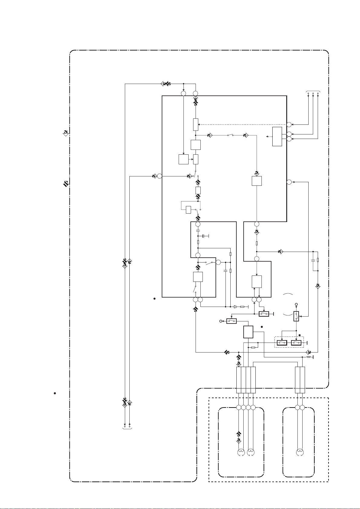
Video Block Diagram
MODE: SP/RECPB-VIDEO SIGNAL DVD VIDEO SIGNAL
VIDEO (L)-1
HEAD
VIDEO (R)-1
HEAD
VIDEO (L)-2
HEAD
CYLINDER ASSEMBLY
VIDEO (R)-2
HEAD
MAIN CBA
REC-VIDEO SIGNAL
TO SERVO/SYSTEM
CONTROL BLOCK
DIAGRAM
IIC-BUS SCL
IIC-BUS SDA
:INDICATES A TEST POINT WITH A JUMPER WIRE ACROSS A HOLE IN THE PCB.
:USED TO INDICATE A TEST POINT WITH A COMPONENT LEAD ON FOIL SIDE.
:USED TO INDICATE A TEST POINT WITH NO TEST PIN.
:USED TO INDICATE A TEST POINT WITH A TEST PIN.
TEST POINT INFORMATION
(DECK ASSEMBLY)
TO SERVO/SYSTEM
CONTROL BLOCK
456
123
CN251
VIDEO(L)-1
VIDEO(L)-2
VIDEO(R)-1
VIDEO-COM
969594
7978
46 43
6968
SERIAL
DECORDER
65
50
55
P
R
Y. DELAY
VIDEO-COM
93
SP
HEAD
AMP
SP
EP
LUMINANCE
SIGNAL
PROCESS
AGC
BYPASS
VIDEO(R)-2
908988
WF1
EP
CHARA.
RF-SW
D-REC-H
RF-SW
TP504
87
80
HEAD
AMP
D-REC-H
REC FMAGC
+
Y
C
CCD 1H DELAY
1/2
FBC
INS.
DIAGRAM
H-A-SW
C-ROTA
D-V-SYNC
H-A-COMP
83
71
62
70
H-A-SW
D-V-SYNC
H-A-COMP
RF-SW/C-ROTA
RPRP
CHROMINANCE
SIGNAL
PROCESS
V-ENV
C-SYNC
84
V-ENV
Y/C
PR
TRICK-H
SECAM-H
67
C-SYNC
VXO
MIX
AGC
PAL/SECAM
DETECTOR
IC370 (PAL/SECAM DECTECTOR)
1
171418216
29
28
44
PB-H OUT
21
WF2
C-PB
TP301
25
2928
X301
4.43MHz
58 59
“ “ = SMD
NOTE FOR WIRE CONNECTORS:
1. PREFIX SYMBOL "CN" MEANS CONNECTOR.
(CAN DISCONNECT AND RECONNECT.)
2. PREFIX SYMBOL "CL" MEANS WIRE-SOLDER
HOLES OF THE PCB.
(WIRE IS SOLDERED DIRECTLY.)
WF3
IC501 (OSD)
OSD-V-OUT
J909
COLOR
-IN
OSD
CHARACTER
MIX
52
BUFFER
Q301
VIDEO SIGNAL PROCESS
/HEAD AMP
IC301
CN253
WF7
VIDEO-OUT 9
50
VIDEO-IN 7
WF6
1-4-2
HK100BLV
Page 12
Audio Block Diagram
Mode : SP/REC
ALC
12
DET
11
MUTE
LINE
ALC
AMP
REC-ON
SERIAL
DECODER
71
68 69
TO SERVO/SYSTEM
CONTROL BLOCK
DIAGRAM
IIC-BUS SCL
IIC-BUS SDA
AUDIO-MUTE-H
PB-AUDIO SIGNAL REC-AUDIO SIGNAL
MAIN CBA
15
IC301
(AUDIO SIGNAL PROCESS)
INV
PB-ON
P
R
ATT
98
7
EQ
AMP
SP/LP-ON
5
6
P-ON+5V
Q404
Q403
BIAS
OSC
REC
AUTO
1
AMP
100
3
BIAS
2
Q406
16
AUDIO HD-SW
CONTROL
P-ON+5V
SWITCHING
D-REC-OFF
Q405
Q401
(PB=ON)
NOTE FOR WIRE CONNECTORS:
1. PREFIX SYMBOL "CN" MEANS CONNECTOR.
(CAN DISCONNECT AND RECONNECT.)
2. PREFIX SYMBOL "CL" MEANS WIRE-SOLDER
HOLES OF THE PCB.
(WIRE IS SOLDERED DIRECTLY.)
“ “ = SMD
N-A-PB
N-A-REC
TO Hi-Fi AUDIO
BLOCK DIGRAM
1-4-3
CN504
ACE HEAD ASSEMBLY
(DECK ASSEMBLY)
AUDIO-PB/REC
4
3 A-COM
1 AE-H
2 AE-H/FE-H
AUDIO
HEAD
AUDIO
ERASE
HEAD
CN501
2 FE-H
FE HEAD
FULL
ERASE
HK100BLA
1 FE-H-GND
HEAD
Page 13
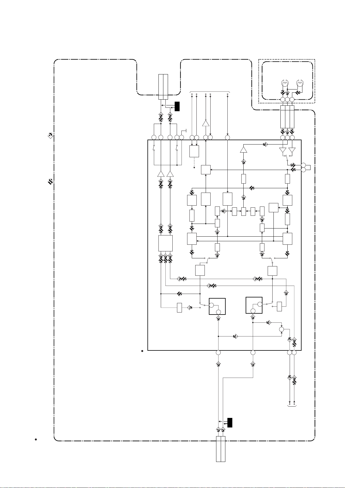
Hi-Fi Audio Block Diagram
REC-AUDIO SIGNALPB-AUDIO SIGNAL Mode : SP/REC
CN253
73
MUTE-ON
AUDIO(R)-OUT
AUDIO(L)-OUT
5
4
74
767775
WF5
MUTE-ON
A-MODE
IIC-BUS SCL
IIC-BUS SDA
Q451
37
38
LOGIC
FROM/TO
SERVO/SYSTEM
CONTROL BLOCK
AUDIO-MUTE-H
21
53
MUTE
Hi-Fi-H-SW
39
Hi-Fi
AUDIO
(R) HEAD
CYLINDER
ASSEMBLY
(DECK ASSEMBLY)
-COM 8
CN251
Hi-Fi-AUDIO(R)7Hi-Fi
242627
R
Hi-Fi
9
Hi-Fi-AUDIO(L)
L
AUDIO
(L) HEAD
MAIN CBA
R-CH
SW
OUTPUT
SELECT
ALC
(Hi-Fi AUDIO SIGNAL PROCESS)
BPF
COMP
NOISE
R-CH
ENV
NOISE
PPR
PNR
DET
DET
34 33
LIM
L-CH
DET
PNR
ALC
BPF
COMP
SW
NOISE
+
HOLD
PULSE
15
VCO
LIM DEV
DO
R
L-CH
LPF
MIX V/I
VCO
LIM DEV
47
48
LPF
14
NOTE FOR WIRE CONNECTORS:
“ “ = SMD
1. PREFIX SYMBOL "CN" MEANS CONNECTOR.
(CAN DISCONNECT AND RECONNECT.)
2. PREFIX SYMBOL "CL" MEANS WIRE-SOLDER
HOLES OF THE PCB.
(WIRE IS SOLDERED DIRECTLY.)
IC451
1-4-4
52
2AUDIO(R)-IN
CN253
WF4
1AUDIO(L)-IN
6
78
80
N-A-REC
N-A-PB
TO AUDIO BLOCK
HK100BLH
Page 14

SCHEMATIC DIAG RAMS / CBA'S AND TEST POINTS
Standard Notes
WARNING
Many electrical and mechanical parts in this chassis
have special characteristics. These characteristics
often pass unnoticed and the protection afforded by
them cannot necessarily be obtained by using
replacement components rated for higher voltage,
wattage, etc. Replacement parts that have these special safety character istics are id entified in th is manual
and its supplements; electrical components having
such features are identified by the mark " ! " in the
schematic diagram and the par ts list. Before replacing
any of these components, read the parts list in this
manual carefully. The use of substitute replacement
parts that do not have the same safety characterist ics
as specified in the pa r ts list may create sh ock, fire, or
other hazards.
Capacitor Temperature Markings
Mark
(B)
(F)
(SR)
(Y)
Capacity
change rate
±10%
±30 - 80%
±15%
±22.5%
Capacitors and transistor s are represente d by the following symbols.
Standard
Temperature
temperature
20°C -25~+85°C
20°C –25~+85°C
20°C –25~+85°C
20°C –25~+85°C
range
Notes:
1. Do not use the part number shown on th ese drawings for ordering. The correct part number is
shown in the parts list, and may be slightly different
or amended since these drawings were prepared.
2. To maintain original function and reliability of
repaired units, use only orig inal replacement par ts
which are listed with their part numbers in the parts
list section of the service manual.
3. How to read converged lines.
1-D3
Distinction Area
Line Number
(1 to 3 digits)
Examples:
1. "1-D3" means that line number "1" goes to the line number
"1" of the area "D3".
2. "1-B1" means that line number "1" goes to the line number
"1" of the area "B1".
4. All resistance values are indicated in ohms
3
(K=10
, M=106).
5. Resistor wattages ar e 1/4W or 1/6 W unless otherwise specified.
6. All capacitance values are indicated in µF
-6
(P=10
µF).
7. All voltages are DC voltages unless otherwise
specified.
8. Voltage indications for PLAY and REC modes on
the schematics are as shown below.
3
AREA D3
2
1
AREA B1
1-D3
ABCD
1-B1
< PCB Symbols >
(Top View) (Bottom View)
+
(Bottom View)
Transistor or Digital Transistor
E C B
(Top View)
NPN Transistor
E C B
(Top View)
NPN Digital Transistor
E C B
Electrolytic Capacitor
(Top View)
E C B
(Top View)
E C B
Unit: Volts
The same voltage for
both PLAY & REC modes
PNP Transistor
PNP Digital
Transistor
PLAY mode
REC mode
5.0
231
5.0
(2.5)
Indicates that the voltage
is not consistent here.
< Schematic Diagram Symbols >
Digital Transistor
1-5-1 SC_08
Page 15

Main 1/4 Schematic Diagram Parts Location Guide
Ref No. Position Ref No. Position Ref No. Position
CAPACITORS
C502 A-4 C562 C-4 R539 C-4
C505 E-1 R540 C-4
C506 B-1
C508 C-1
C509 A-2
C510 A-2 CN505 F-2 R545 C-1
C511 B-3 CN653 A-1 R546 C-1
C512 A-2
C514 A-2 D510 D-4 R560 D-4
C515 B-3 D555 E-3 R567 E-4
C516 B-2 R568 E-4
C517 B-2 IC501 C-3 R569 E-4
C518 B-3 IC502 B-4 R570 D-1
C519 B-2 R572 D-4
C521 B-2 L501 E-3 R574 E-3
C522 B-1 L502 D-4 R577 E-3
C524 B-4 L503 E-3 R578 E-3
C527 C-1 R582 E-2
C531 E-4 Q506 E-1 R583 E-2
C533 E-4 Q515 E-2 R585 E-2
C534 D-4 R586 E-2
C535 D-4
C536 D-4 R511 A-1 R595 B-3
C538 D-4 R512 E-1 R596 B-3
C539 E-3 R513 E-1 R597 B-3
C540
C541 E-3 R516 A-1
C542 E-2 R517 E-3 SW506 D-1
C545 E-3 R519 A-1 SW507 A-1
C546 E-3
C547 E-3 R525 A-3 VR501 B-1
C548 E-2 R526 A-3
C549 E-2 R528 B-1 X501 E-2
C550E-2R530C-4
C553 E-2 R531 C-4 PS502 E-1
C555E-4R532C-4
C557 A-2 R533 C-4 TP502 A-4
C559 C-4 R536 B-2 TP503 A-2
C560 C-4 R537 B-2 TP504 C-1
C561 C-4 R538 B-4 TP505 C-1
E-3 R514 A-1 R598 C-1
CONNECTORS
CN501 A-2
CN502 F-4
CN504 A-3
DIODES
ICS
COILS
TRANSISTORS
RESISTORS
R509
R523
E-1
A-1
RESISTORSCAPACITORS
R541 B-1
R542 B-1
R543 B-1
R559
R588
SWITCHES
VARIABLE RESISTOR
CRYSTAL OSCILLATOR
MISCELLANEOUS
TEST POINTS
E-3
F-3
1-5-2
Page 16
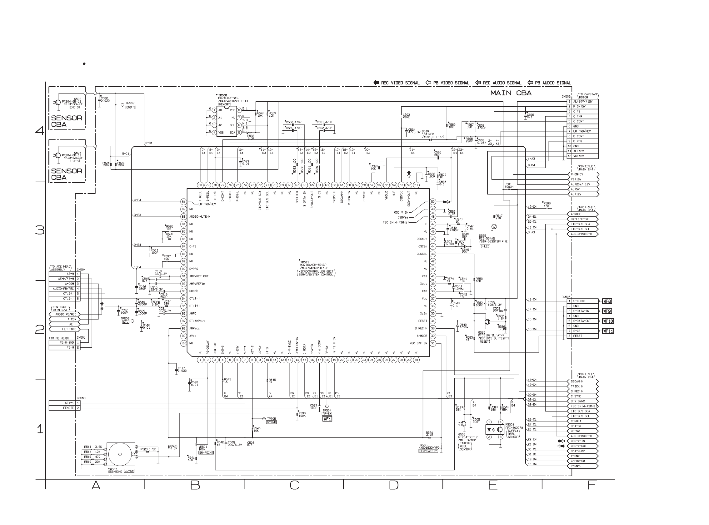
Main 1/4 & Sensor Schematic Diagram
“ “ = SMD
1-5-3
HK100SCM1
Page 17

Main 2/4 Schematic Diagram
“ “ = SMD
1-5-4
HK100SCM2
Page 18

Main 2/4 Schematic Diagram Parts Location Guide
Ref No. Position Ref No. Position Ref No. Position Ref No. Position
CAPACITORS
C151 K-1 C344 J-4 L251 H-3 R328 I-4
C152 K-1 C345 J-4 L302 I-4
C251 H-3 C348 K-4 L401 G-2
C252 H-3 C349 J-4 L402 H-1
C253 H-3 C350 H-4
C254 H-3 C402 G-2 Q151 K-2
C301 J-1 C403 G-2 Q152 K-1
C302 J-2 C404 H-2 Q153 K-1
C303 J-1 C405 H-2 Q301 K-4 R401 G-2
C305 J-1 C407 I-1 Q302 H-3 R402 G-2
C306 J-2 C408 I-2 Q401 G-1
C307 J-1 C409 I-1 Q403 H-1 R405 H-2
C308 J-1 C410 I-1 Q404 G-2
C311 K-3 C411 I-1 Q405
C312 K-3 C412 I-2 Q406 H-1
C313 K-3 C413 I-2 R409 H-2
C314 K-3 C414 I-1 R151 K-1 R410 H-2
C315 K-2 C415 I-1 R152 K-1 R411 I-2
C316 K-3 C416 I-1 R153 K-2 R412 I-1
C317 K-3 C417 I-2 R251 H-3 R413 I-2
C318 K-2 C418 I-1 R252 H-3 R414 I-1
C321 L-3 C419 J-1 R301 J-1 R415 I-1
C322 K-3 C420 J-2 R303 J-1 R416 I-1
C324 K-3 C421 J-1 R305 K-2 R417 I-1
C325 K-2 C422 L-4 R308 K-2 R418 I-1
C328 K-3 C423 L-4 R309 J-4 R419 I-1
C329 K-2 C426 L-3 R310 K-3 R420 I-1
C330 L-4 C427 L-3 R312 K-2 R421 J-1
C331 K-4 R314 K-2
C333 I-4 CN251 G-3 R316 G-4 X301 J-2
C334 I-4 CN252 L-2 R317 J-4
C335 I-4 CN253 L-4 R318 K-4 TP301 G-3
C336 I-4 R319 H-3
C337 I-4 D151 K-1 R320 H-3
C339 I-4 D301 Q-4 R321 K-4
C340 I-4 R322 H-4
C341 I-4 IC301 Q-2 R325 I-4
C342 I-4 R326 I-4
C343 J-4 L151 L-1 R327 I-4
CAPACITORS
CONNECTORS
DIODES
IC
COILS
COILS
TRANSISTORS
H-1 R407
RESISTORS
RESISTORS
R330
R331
R332
R333
R334
R336
R337
R404
R406
R408
CRYSTAL OSCILLATOR
TEST POINT
I-4
H-4
H-4
I-4
I-4
J-4
J-4
H-1
H-2
H-2
H-2
1-5-5
Page 19

Main 3/4 Schematic Diagram Parts Location Guide
Ref No. Position Ref No. Position Ref No. Position
CAPACITORS
C452O-2C475O-4R462Q-2
C4 53 O-2 C47 6 O-4 R46 3 P-2
C454 O-2 C478 N-3 R464 P-3
C455O-2C479N-3R466O-4
C456O-2C482N-3R467N-4
C457O-2C483N-3R470N-4
C458 P-2 C484 N-2
C461 Q-2 C485 N-2
C462 P-2 C486 N-2
C463 P-2 C487 N-1
C464 P-2 C489 N-1
C465 P-3 R484 M-2
C466 P-3 IC451 N-2
C467 P-3
C468 P-3 L451 P-3
C469 P-4 L452 Q-2
C470 P-4
C4 71 O-4 Q451 Q-2
C472 O-4
C473 O-4 R453 N-1
C474 O-4 R454 N-1
IC
COILS
TRANSISTOR
RESISTORS
RESISTORSCAPACITORS
R479
R480
R481
R482
R483
M-3
M-3
M-2
M-2
M-2
1-5-6
Page 20

Main 3/4 Schematic Diagram
“ “ = SMD
1-5-7
HK100SCM3
Page 21

Main 4/4 Schematic Diagram
“ “ = SMD
MAIN 4/4 Schematic Diagram
Parts Location Guide
Ref No. Position
CAPACITORS
C370 S-2
C371 S-2
C372 S-2
C373 S-2
C374 T-1
C375 T-1
C376 T-1
C377 T-2
C378 T-2
C379 S-2
C381 T-2
C382 S-2
C383 S-2
C384 R-2
DIODE
D370 R-1
IC
IC37 0 R-2
COIL
L370 T-2
RESISTORS
R370
R371
R372 R-2
S-2
S-2
1-5-8
HK100SCM4
Page 22
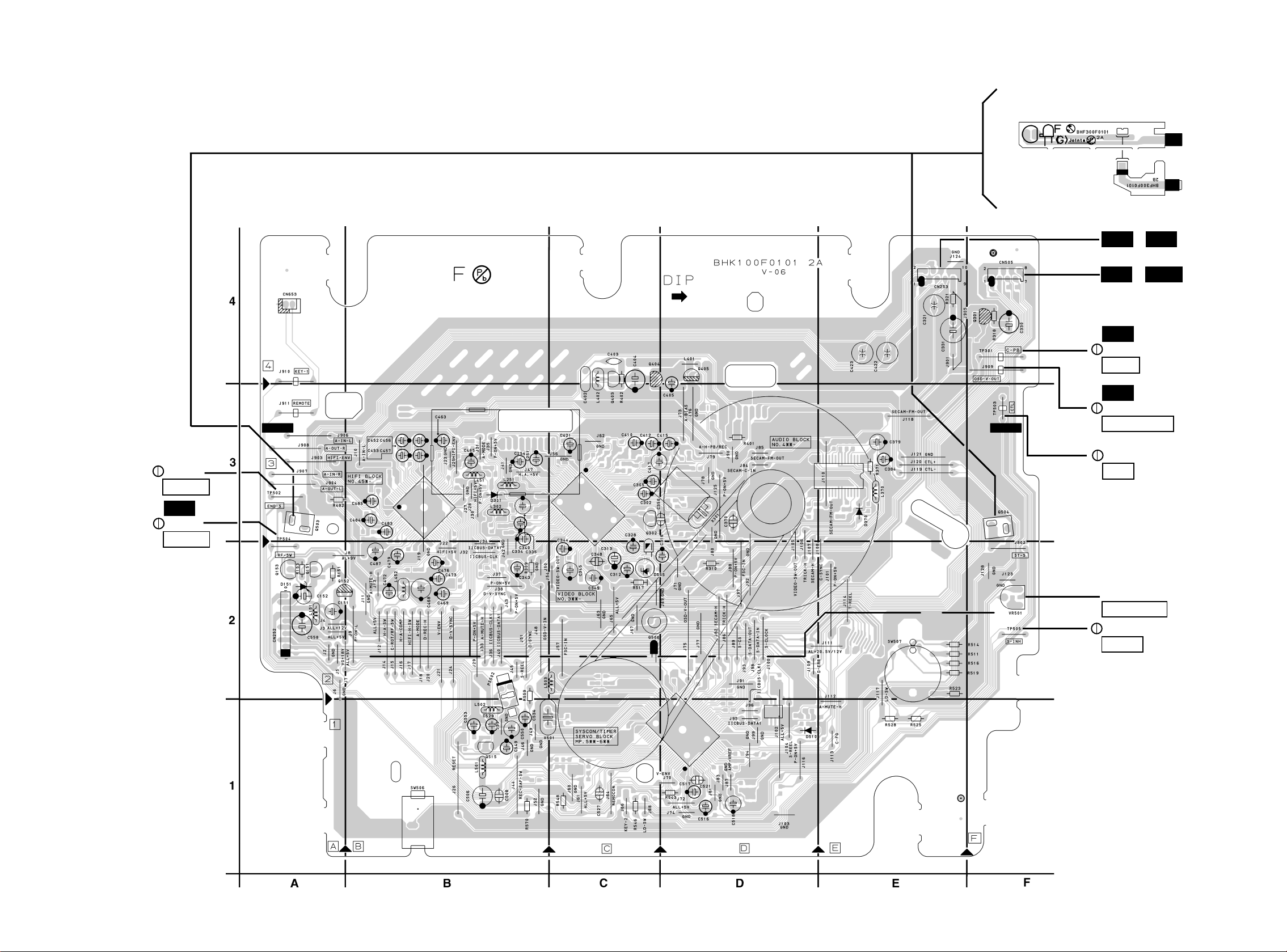
Main CBA Top View
Sensor CBA Top View
BHF300F01012A
BHF300F01012B
WF4 WF7
~
CN253
WF8 WF11
~
CN505
WF2
TP301
C-PB
WF3
J909
OSD-V-OUT
TP502
END-S
WF1
TP504
RF-SW
TP503
CTL
VR501
SW-POINT
TP505
S-INH
1-5-9
BHK100F01012A
Page 23

Main CBA Bottom View
1-5-10
BHK100F01012A
Page 24
Main CBA Parts Location Guide
Ref No. Position Ref No. Position Ref No. Position Ref No. Position
D555 C-2 R308 D-3 R418 C-3 R545 C-1
R309 B-2 R419 D-3 R546 C-1
IC301 C-3 R310 D-2 R420 D-3
R559
B-2
IC370 D-3 R312 D-3 R421 D-3 R560 D-2
IC451 B-3 R314 D-2 R453 B-3 R567 D-2
IC501 D-1 R316 D-3 R454 B-3 R568 D-2
IC502 D-2 R317 F-4 R462 B-3 R569 E-1
R318 F-4 R463 B-3 R570 B-1
L151 A-2 R319 D-3 R464 B-3 R572 D-2
L251 B-3 R320 B-3 R466 B-2 R574 C-1
L302 B-3 R321 E-4 R467 B-2 R577 C-1
L370 E-3 R322 B-3 R470 B-2 R578 C-2
L401 D-4 R325 B-3 R479 B-3 R582 B-1
L402 C-3 R326 B-3 R480 B-3 R583 B-1
L451 B-3 R327 B-3 R481 B-3 R585 B-1
L452 B-2 R328 B-3 R482 A-3 R586 B-1
L501 B-1 R330 B-3 R483 B-3 R588 B-2
L502 B-1 R331 B-2 R484 B-3 R595 D-1
L503 B-2 R332 B-2 R509 B-2 R596 D-1
R333 C-1 R511 F-2 R597 D-1
Q151 A-2 R334 B-1 R512 B-1 R598 C-1
Q152 A-2 R336 B-2 R513 E-1
Q153 A-2 R337 B-2 R514 F-2 SW506 B-1
Q301 F-4 R370 E-3 R516 F-2 SW507 E-2
Q302 C-3 R371 E-3 R517 C-2
Q401 D-3 R372 E-3 R519 F-2 VR501 F-2
Q403 C-3 R401 D-3 R523 E-2
Q404 C-4 R402 C-3 R525 E-1 X301 D-3
Q405 D-4 R404 C-3 R526 C-1 X501 B-1
Q406 B-3 R405 C-3 R528 E-1
Q451 B-3 R406 D-4 R530 D-2 PS502 B-2
Q506 C-2 R407 B-3 R531 D-2
Q515 B-1 R408 C-3 R532 D-1 TP301 F-4
R409 C-3 R533 D-1 TP502 A-3
R151 A-2 R410 C-3 R536 D-1 TP503 F-3
R152 A-2 R411 C-3 R537 D-1 TP504 A-3
R153 A-2 R412 C-3 R538 D-1 TP505 F-2
R251 B-3 R413 C-3 R539 D-2
R252 B-3 R414 C-3 R540 D-2
R301 D-3 R415 C-3 R541 F-2
R303 D-3 R416 C-3 R542 D-1
R305 D-2 R417 D-3 R543 D-1
RESISTORS
TEST POINTS
RESISTORS
SWITCHES
RESISTORS RESISTORS
VARIABLE RESISTORS
DIODES
CRYSTAL OSCILLATORS
MISCELLANEOUS
ICS
TRANSISTORS
COILS
Ref No. Position Ref No. Position Ref No. Position Ref No. Position
CAPACITORSCAPACITORS CAPACITORS
C151 A-2 C349 C-2 C455 B-3 C519 D-1
C152 A-2 C350 C-3 C456 B-3 C521 D-1
C251 B-3 C370 D-3 C457 B-3 C522 D-1
C252 B-3 C371 E-3 C458 B-3 C524 E-1
C253 B-3 C372 E-3 C461 B-3 C527 C-1
C254 B-3 C373 E-3 C462 B-3 C531 D-1
C301 D-3 C374 D-3 C463 B-3 C533 E-1
C302 C-3 C375 D-3 C464 B-3 C534 B-1
C303 C-3 C376 D-3 C465 B-3 C535 D-2
C305 C-3 C377 E-3 C466 B-3 C536 D-2
C306 D-3 C378 E-3 C467 B-3 C538 D-2
C307 D-3 C379 E-3 C468 B-2 C539 C-2
C308 D-3 C381 E-3 C469 B-2 C540 C-2
C311 C-2 C382 E-3 C470 B-2 C541 C-1
C312 C-2 C383 E-3 C471 B-2 C542 C-1
C313 C-2 C384 E-3 C472 B-2 C545 C-2
C314 D-2 C402 C-3 C473 B-2 C546 C-1
C315 D-3 C403 C-4 C474 B-2 C547 C-2
C316 D-3 C404 C-4 C475 B-3 C548 C-1
C317 D-2 C405 D-3 C476 B-2 C549 B-1
C318 D-3 C407 C-3 C478 B-2 C550 B-1
C321 E-4 C408 C-3 C479 B-2 C553 B-1
C322 D-2 C409 C-3 C482 B-2 C555 E-2
C324 C-2 C410 C-3 C483 B-3 C557 D-1
C325 D-3 C411 C-3 C484 B-3 C559 F-4
C328 C-3 C412 C-3 C485 B-3 C560 F-4
C329 D-2 C413 C-3 C486 B-3 C561 F-4
C330 F-4 C414 C-3 C487 B-2 C562 F-4
C331 E-4 C415 C-3 C489 B-2
C333 B-3 C416 D-3 C502 A-3 CN251 B-3
C334 B-2 C417 C-3 C505 D-2 CN252 A-2
C335 B-2 C418 D-3 C506 B-1 CN253 E-4
C336 B-3 C419 D-3 C508 B-1 CN501 B-3
C337 B-3 C420 B-3 C509 D-1 CN502 E-2
C339 B-3 C421 C-3 C510 D-1 CN504 D-3
C340 B-2 C422 E-4 C511 D-1 CN505 F-4
C341 B-3 C423 E-4 C512 D-1 CN653 A-4
C342 D-2 C426 E-4 C514 D-1
C343 B-2 C427 E-4 C515 D-1 D151 A-2
C344 C-3 C452 B-3 C516 D-1 D301 B-3
C345 C-2 C453 B-3 C517 D-1 D370 E-3
C348 C-2 C454 B-3 C518 D-1 D510 D-1
CAPACITORS
CONNECTORS
DIODES
1-5-11
Page 25

WAVEFORMS
NOTE:
Input
VCR: COLOR BAR SIGNAL (WITH 1KHz AUDIO SIGNAL)
(WF1~WF11)
WF2
UPPER
TP301
WF1
LOWER
TP504
C-PB 10mV x 10
RF-SW 0.5V x 10
5ms
WF3
UPPER
J909
WF1
LOWER
TP504
V-OUT 0.1V x 10
RF-SW 0.5V x 10
50µs
WF4
Pin 1, 2 of CN253
AUDIO( L,R )-IN 1V
WF5
Pin 4, 5 of CN253
AUDIO( L,R )-OUT 1V
2.5ms
WF8
Pin 1 of CN505
S-CLK 1V0.5ms 1ms
WF9
Pin 3 of CN505
S-DATA-IN 1V 1ms
MAIN
CBA
WF3
J909
V-OUT E-E
10µs 50mV x 10
WF6
Pin 7 of CN253
VIDEO-IN 0.2V
WF7
Pin 9 of CN253
VIDEO-OUT 0.2V
20µs
20µs
WF10
Pin 5 of CN505
S-DATA-OUT 1V 1ms
WF11
Pin 7 of CN505
S-CS 1V 20ms
CN252 CN253 CN505
Pin No. Voltage WF No. Pin No. Voltage WF No. Pin No. Voltage WF No.
1 18.1 1 WF4 1 WF8
20 2 WF4 2 0
3 12.7 3 0 3 WF9
4 12.1 4 WF5 4 0
50 5 WF5 5 WF10
6 12.0 6 0 6 0
70 7 WF6 7 WF11
85.3 8 0 8 4.8
90 9 WF7
10 0 10 0
1-6-1
U31MWF
Page 26

1
KEY-1
CN653
2
REMOTE
WIRING DIAGRAM
1
2
3
4
5
6
7
8
9
10
GND
GND
GND
GND
CN252
VG+18V
AL+12V
AL+20V/+12V
AL+12V
AL+5V
CN253
C-POW-SW
MAIN CBA
1AUDIO(L)-IN
2AUDIO(R)-IN
3
GND
4AUDIO(L)-OUT
5AUDIO(R)-OUT
6
7VIDEO-IN
GND
8
9VIDEO-OUT
GND
10GND
1S-CLOCK
CN505
2GND
3
S-DATA-IN
4GND
5S-DATA-OUT
6
GND
7S-CS
8
RESET
NOTE FOR WIRE CONNECTORS:
1. PREFIX SYMBOL "CN" MEANS CONNECTOR.
(CAN DISCONNECT AND RECONNECT.)
SENSOR CBA
2. PREFIX SYMBOL "CL" MEANS WIRE-SOLDER
HOLES OF THE PCB.
(WIRE IS SOLDERED DIRECTLY.)
SENSOR CBA
CN504
AE-H2AE-H/FE-H
A-COM4AUDIO-PB/REC
1
AUDIO
ACE HEAD ASSEMBLY
CTL(+)6CTL(-)1FE-H-GND
3
5
AUDIO HEAD
ERASE HEAD
CONTROL HEAD
CN501
FE-H
2
FULL
ERASE HEAD
FE HEAD
CAPSTAN
MOTOR
CN502
AL+20V/+12V
P-ON+5V3C-FG4C-F/R5C-CONT6GND7LM-FWD/REV
1
2
M
M
LOADING
CYLINDER ASSEMBLY
MOTOR
MOTOR
PG
DRIVE
CIRCUIT
SENSOR
D-CONT9D-PFG
GND11AL+12V12VG+18V
8
10
M
DRUM
MOTOR
VIDEO
(R)1
CAPSTAN
VIDEO
HEAD
CN251
VIDEO(R)-1
1
MOTOR
(L)1
HEAD
VIDEO-COM
VIDEO(L)-1
VIDEO(L)-2
2
3
4
VIDEO
VIDEO
(L)2
HEAD
VIDEO-COM
VIDEO(R)-2
Hi-Fi-AUDIO(R)
Hi-Fi-COM9Hi-Fi-AUDIO(L)
5
6
7
8
(R)2
HEAD
Hi-Fi AUDIO
(R) HEAD
Hi-Fi AUDIO
(L) HEAD
(DECK ASSEMBLY)
1-7-1
HK100WI
Page 27

IC PIN FUNCTION DESCRIPTIONS
IC501( SERVO / SYSTEM CONTROL IC )
“H” ≥ 4.5V, “L” ≤ 1.0V
Pin
IN/
Signal
No.
OUT
1 - NU Not Used -
2IN
3INPOW-SAF
4 IN END-S
5 - NU Not Used 6INV-ENV
7INKEY-1
8INKEY-2
9INLD-SW
10 IN ST-S
11 - NU Not Used -
12 - NU Not Used 13 OUT
14 IN
15 OUT C-ROTA
16 OUT H-A-SW
17 IN
18 OUT RF-SW
19 OUT
20 - NU Not Used -
21 - NU Not Used 22 - NU Not Used 23 - NU Not Used 24 - NU Not Used 25 - NU Not Used -
Name
PGDELAY
D-VSYNC
REMOCON
-IN
H-ACOMP
Hi-Fi-H-SWHi-Fi Audio Head
Function
Video Head Switching
Pulse Signal Adjusted
Voltage
P-ON Power
Detection Input Signal
Tape End Position
Detect Signal
Video Envelope
Comparator Signal
Key Scan Input Signal
1
Key Scan Input Signal
2
Deck Mode Position
Detector Signal
Tape Start Position
Detector Signal
Dummy V-sync
Output
Remote Control
Sensor
Color Phase Rotary
Changeover SIgnal
Video Head Amp
Switching Pulse
Head Amp
Comparator Signal
Video Head Switching
Pulse
Switching Pulse
Active
Level
A/D
A/D
A/D
A/D
A/D
A/D
A/D
A/D
H/Hi-z
H/L
H/L
H/L
H/L
H/L
Pin
IN/
Signal
No.
OUT
26 - NU Not Used 27 - NU Not Used 28 - NU Not Used 29 - NU Not Used 30 - NU Not Used -
31 IN
32 IN A-MODE
33 OUT D-REC-H
34 IN RESET
35 IN Xcin Sub Clock (GND) -
36 - NU Not Used 37 - Vcc Vcc 38 IN Xin Main Clock Input 39 OUT Xout Main Clock Input 40 - Vss Vss(GND) 41 - NU Not Used 42 - NU Not Used -
43 IN CLKSEL
L
44 IN OSCin
45 OUT OSCout
46 - NU Not Used -
47 - LP LP 48 IN
49 - OSDVss OSDVss 50 IN OSD-V-IN
51 - NU Not Used 52 OUT
53 - OSDVcc OSDVcc 54 - HLF
Name
RECSAF-SW
FSC-IN
[4.43MHz]
OSD-VOUT
Function
Recording Safety SW
Detect (With Record
tab="L"/With out
Record tab="H")
Hi-Fi Tape Detecti on
Signal
Delayed Record
Signal
System Reset Signal
(Reset=”L”)
Clock Select (VCC
Pull UP)
Clock Input for letter
size
Clock Output for letter
size
4.43MHz Clock Input -
OSD Video Signal
Input
OSD Video Signal
Output
LPF Connected
Terminal (Slicer)
Active
Level
H
L
H
L
-
-
-
-
-
-
1-8-1 HK100PIN
Page 28
Pin
No.
IN/
OUT
Signal
Name
Function
Active
Level
Pin
No.
IN/
OUT
Signal
Name
Function
Active
Level
55 - VHOLD COLOR-IN 56 - NU Not Used 57 - NU Not Used -
58 IN C-SYNC
Composite
Synchronized Pulse
PULSE
59 - NU Not Used 60 OUT
61 IN
62 OUT
C-POW-SWCapstan Power
Switching Signal
SECAM-HSECAM Video Signal
Input
TRICK-H
Special playback =
“H” in SECAM Mode
H/L
63 - NU Not Used 64 IN S-CS
65 OUT
66 IN
S-DATAOUT
S-DATA-INDVD (MCU) SIO
DVD (MCU) SIO
Interface CS
DVD (MCU) SIO
Interface Clock Out
Interface Data In
H/L
H/L
83 OUT
A-MUTE-HAudio Mute Control
Signal
H
84 - NU Not Used 85 - NU Not Used 86 - NU Not Used -
Capstan Motor
87 IN C-FG
Rotation Detection
PULSE
Pulse
88 - NU Not Used (GND) -
H
H
L
89 - NU Not Used 90 IN D-PFG
91 -
92 -
AMPVRE
F OUT
AMPVRE
Fin
Drum Motor Pulse
Generator
PULSE
V-Ref for CTL AMP -
V-Ref for CTL AMP 93 - P80/C P80/C Terminal 94
IN/
OUT
CTL (-)
Playback/Record
Control Signal (-)
H/L
67 OUT S-CLOCK
DVD (MCU) SIO
Interface Clock
H/L
68 - NU Not Used 69 - NU Not Used 70 - NU Not Used -
71 OUT
IN/
72
OUT
IIC-BUS
SCL
IIC-BUS
SDA
2
I
C BUS Control
Clock
2
I
C BUS Control Data
H/L
H/L
73 - NU Not Used 74 - NU Not Used -
75 OUT P-ON-L
76 OUT C-CONT
77 OUT D-CONT
Power On Signal at
Low
Capstan Motor
Control Signal
Drum Motor Control
Signal
PWM
PWM
Capstan Motor FWD/
78 OUT C-F/R
REV Control Signal
H/L
(FWD=”L”/REV=”H”)
IN/
95
OUT
CTL (+)
96 - AMPC
97 -
CTLAMP
out
Playback/Record
Control Signal (+)
CTL AMP Connected
Terminal
To Monitor for CTL
AMP Output
H/L
-
PULSE
98 - AMPVcc AMPVcc -
A/D Converter Power
99 - AVcc
Input/ Standard
-
Voltage Input
100 - NU Not Used -
Notes:
L
Abbreviation for Active Level:
PWM -----Pulse Wide Modulation
A/D--------Analog - Digital Converter
79 IN S-REEL
80 IN T-REEL
81 OUT
LM-FWD/
REV
Supply Reel Rotation
Signal
Take Up Reel
Rotation Signal
Loading Motor Control
Signal
PULSE
PULSE
H/L/
Hi-z
82 - NU Not Used -
1-8-2 HK100PIN
Page 29
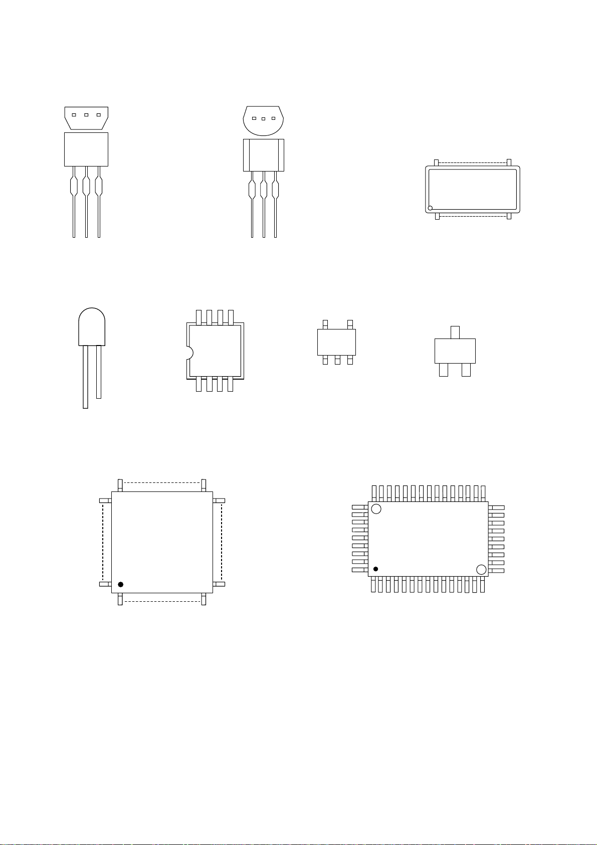
LEAD IDENTIFICATIONS
E C B
MID-32A22F
PT204-6B-12
C
E
KRA103M-AT/P
KRC103M-AT/P
KTA-1266-GR-AT/P
KTC3199-(BL,GR,Y)-AT/P
BR24L02F-WE2
CAT24WC02WI-TE13
8
1
2SA1015-GR(TE2 F T)
2SC1815-(BL,GR,Y)(TE2 F T)
2SC2120-Y(TE2 F T)
2SC3266-Y(TPE2 F)
KTC3203-Y-AT/P
KTC3205-Y-AT/P
KTC3198-(GR,Y)-AT/P
E C B
RN1511(TE85R.F)
C1 C2
5
4
B1 E B2
LA70100M-TRM-E
30
1
KRC103S-RTK/P
KTC3875S-Y-RTK/P
C
16
15
BE
61
80
LA72648M-MPB-E
60
1
41
20
40
21
81
100
LA71750EM-MPB-E
M3776AMCH-AD1GP
M3776AMCH-AF1GP
80
1
51
50
31
30
Note:
A: Anode
K: Cathode
E: Emitter
C: Collector
B: Base
R: Reference
S: Source
G: Gate
D: Drain
1-9-1 HK100LE
Page 30

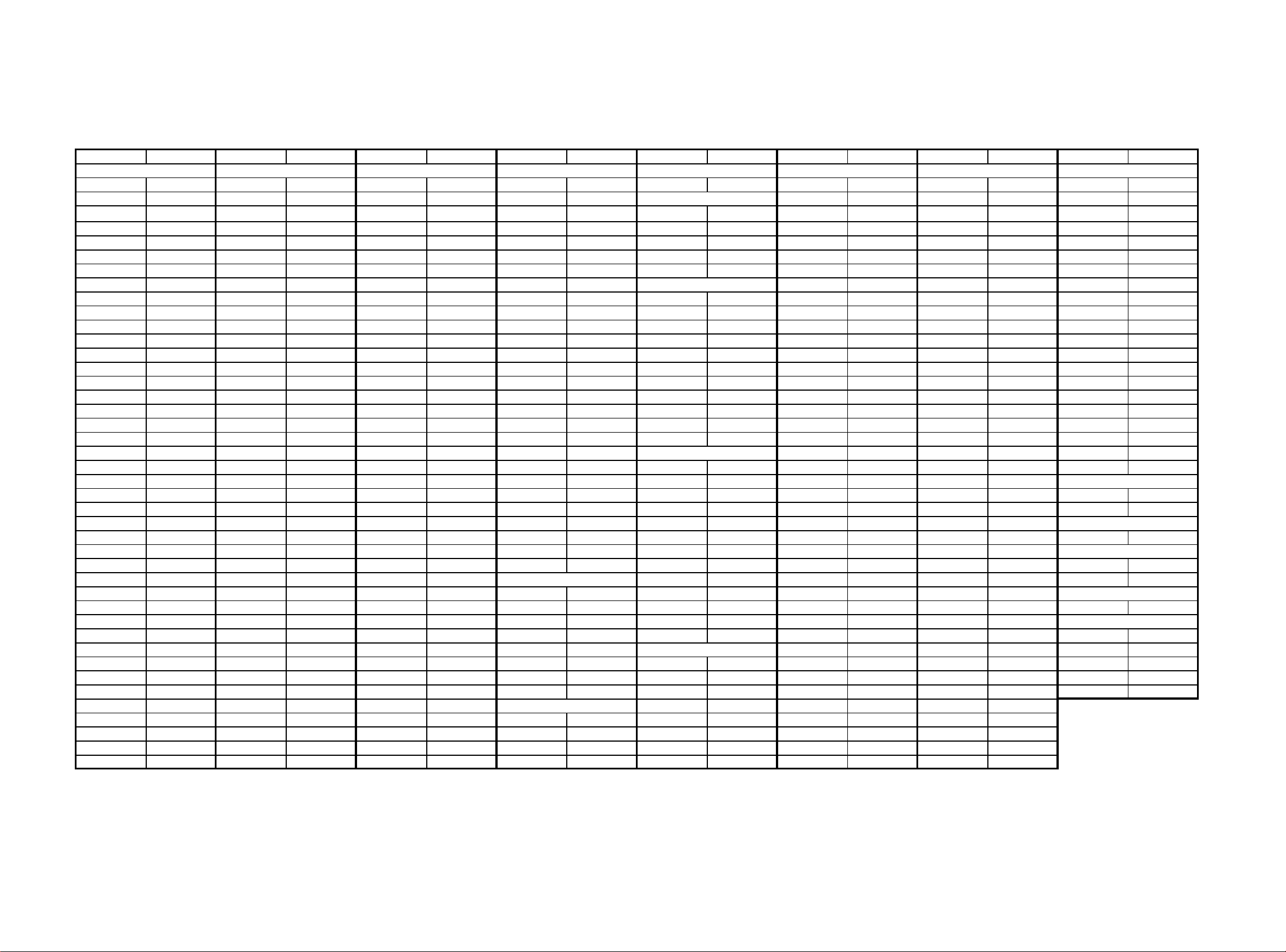
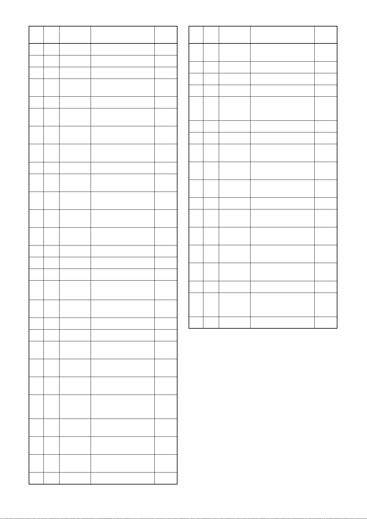
ELECTRICAL PARTS LIST
PRODUCT SAFETY NOTE: Products marked with a
! have special characteristics important to safety.
Before replacing any of these components, read
carefully the product safety notice in this service
manual. Don't degrade the safety of the product through
improper servicing.
NOTES:
Parts that are not assigned par t numbers (---------) ar e
not available.
Tolerance of Capacitors and Resistors are noted with
the following symbols.
C.....±0.25% D .....±0.5% F .....±1%
G.....±2% J......±5% K.....±10%
M.....±20% N.....±30% Z.....+80/-20%
ELECTRICAL PARTS LIST
Pos.No. ! 12 NC Description
MCV CBA 1
Consists of the following:
MAIN CBA 1
SENSOR CBA 1
MAIN CBA
2B7 SHIELD ASSEMBL Y H9500 ED 1
2B8 BUSH LED(F) H3700UD 1
2B46 ROHM HOLDER H7770JD 1
PS502 PHOT O INTE RR UPTE R RPI- 302C70 1
TP301 PCB JUMPER D0.6-P14.0 1
TP502 PCB JUMPER D0.6-P10.0 1
TP503 PCB JUMPER D0.6-P6.0 1
TP504 PCB JUMPER D0.6-P8.0 1
TP505 PCB JUMPER D0.6-P7.5 1
VR501 CARBON P.O. T. VZ067TL1 B104 PB(F) 1
X301 XT AL 4.433619MHZ 1
X301 QUARTZ CR YSTAL 4.433619MHZ 1
X301 XT AL 1K*044334EE 1
X501 QUARTS CR YSTAL 12.000000MHZ 1
X501 XT AL 12MHZ 12.000MHZ 1
CAPACITORS
C151 ELECTR OLYTIC CAP. 47UF/1 6V M H7 1
C151
C152 ELECTR OLYTIC CAP. 10UF/1 6V M H7 1
C152 ELECTR OLYTIC CAP. 10UF/1 6V M H7 1
C251 ELECTR OLYTIC CAP. 10UF/1 6V M H7 1
C251
C252
C252
C253
C254 ELEC TROLYTIC CAP. 1UF/ 50V M H7 1
C254
C301
C301
C302 ELEC TROLYTIC CAP. 1UF/ 50V M H7 1
C302
C303 CHIP CERAMIC CAP. F Z 0.22UF/ 16V 1
C305 ELEC TROLYTIC CAP. 1UF/ 50V M H7 1
ALUMINUM ELECTROL YTIC CAP
47UF/16V H7
ALUMINUM ELECTROL YTIC CAP
10UF/16V H7
CHIP CERAMIC CAP.(1608) F Z 0.1UF/
50V
CHIP CERAMIC CAP.(1608) F Z 0.1UF/
25V
CHIP CERAMIC CAP.(1608) B K
1000PF/50V
ALUMINUM ELECTROL YTIC CAP 1UF/
50V H7
CHIP CERAMIC CAP.(1608) B K
0.022UF/50V
CHIP CERAMIC CAP.(1608) B K
0.022UF/25V
ALUMINUM ELECTROL YTIC CAP 1UF/
50V H7
1
1
1
1
1
1
1
1
1
ELECTRICAL PARTS LIST
Pos.No. ! 12 NC Description
C305
C306
C306
C307
C307
C308
C308
C311
C311
C312 ELECTROL YTIC CAP. 10UF/16V M H7 1
C312
C313 ELECTROL YTIC CAP. 1UF/50V M H7 1
VCR Module
C313 ELECTROL YTIC CAP. 1UF/50V M H7 1
C314
C315
C315
C316 ELECTROL YTIC CAP. 1UF/50V M H7 1
C316
C317
C317
C318
C318
C321
C322
C322
C324
C325 CHIP CERAMIC CAP. B K 8200PF/50V 1
C328 ELECTROL YTIC CAP. 47UF/6.3V M H7 1
C328
C329
C329
C330 ELECTROLYTIC CAP. 100UF/16V M 1
C330 ELECTROLYTIC CAP. 100UF/16V M 1
C331 ELECTROLYTIC CAP. 470UF/6.3V M 1
C331 ELECTROLYTIC CAP. 470UF/6.3V M 1
C333
C333
C334 ELECTROL YTIC CAP. 1UF/50V M H7 1
C334
C335 ELECTROLYTIC CAP. 100UF/6.3V H7 1
C335
C336 CHIP CERAMIC CAP. CH J 220PF/50V 1
ALUMINUM ELECTROL YTIC CAP 1UF/
50V H7
CHIP CERAMIC CAP.(1608) B K
0.047UF/50V
CHIP CERAMIC CAP.(1608) B K
0.047UF/25V
CHIP CERAMIC CAP.(1608) B K
0.022UF/50V
CHIP CERAMIC CAP.(1608) B K
0.022UF/25V
CHIP CERAMIC CAP.(1608) F Z 0.1UF/
50V
CHIP CERAMIC CAP.(1608) F Z 0.1UF/
25V
CHIP CERAMIC CAP.(1608) F Z 0.1UF/
50V
CHIP CERAMIC CAP.(1608) F Z 0.1UF/
25V
ALUMINUM ELECTROL YTIC CAP
10UF/16V H7
CHIP CERAMIC CAP.(1608) B K 0.01UF/
50V
CHIP CERAMIC CAP.(1608) B K
0.047UF/50V
CHIP CERAMIC CAP.(1608) B K
0.047UF/25V
ALUMINUM ELECTROL YTIC CAP 1UF/
50V H7
CHIP CERAMIC CAP.(1608) F Z 0.1UF/
50V
CHIP CERAMIC CAP.(1608) F Z 0.1UF/
25V
CHIP CERAMIC CAP.(1608) B K
0.022UF/50V
CHIP CERAMIC CAP.(1608) B K
0.022UF/25V
ELECTROL YTIC CAP. 47UF/6.3V M NP
H7
CHIP CERAMIC CAP.(1608) F Z 0.1UF/
50V
CHIP CERAMIC CAP.(1608) F Z 0.1UF/
25V
CHIP CERAMIC CAP.(1608) B K 0.01UF/
50V
ALUMINUM ELECTROL YTIC CAP
47UF/6.3V H7
CHIP CERAMIC CAP.(1608) F Z 0.1UF/
50V
CHIP CERAMIC CAP.(1608) F Z 0.1UF/
25V
CHIP CERAMIC CAP.(1608) F Z 0.1UF/
50V
CHIP CERAMIC CAP.(1608) F Z 0.1UF/
25V
ALUMINUM ELECTROL YTIC CAP 1UF/
50V H7
ALUMINUM ELECTROL YTIC CAP
100UF/6.3V H7
VCR Module
1
1
1
1
1
1
1
1
1
1
1
1
1
1
1
1
1
1
1
1
1
1
1
1
1
1
1
1
1
20060508 1-10-1 HK100EL
Page 31

ELECTRICAL PARTS LIST
ELECTRICAL PARTS LIST
Pos.No. ! 12 NC Description
C337
C337
C339 CHIP CERAMIC CAP. CH J 120PF/5 0V 1
C340 ELEC TROLYTIC CAP. 1UF/ 50V M H7 1
C340
C341
C342
C342 CHIP CERAMIC CAP. CH J 10 00PF/25V 1
C343 ELECTR OLYTIC CAP. 10UF/1 6V M H7 1
C343
C344
C345 ELECTR OLYTIC CA P. 0.47UF /50V M H7 1
C345
C348 CERAMIC CAP.(AX) F Z 0.1UF/50 V 1
C349 ELECTR OLYTIC CA P. 0.47UF /50V M H7 1
C349
C350 CERAMIC CAP.(AX) F Z 0.1UF/50 V 1
C370 CERAMIC CAP.(AX) Y M 0.01UF /16V 1
C371
C371
C372
C372
C373
C373
C374
C374
C375
C376
C376
C377
C378
C379 ELECTR OLYTIC CA P. 0.47UF /50V M H7 1
C379
C381
C381
C382 CHIP CERAMIC CAP. B K 2 200PF/50V 1
C383 CHIP CERAMIC CAP. B K 2 200PF/50V 1
C384 ELECTROLYTIC CAP. 2.2UF/50 V M H7 1
C384
C402 FILM CAP.(P) 0.018UF/50V J 1
C402 FILM CAP.(P) 0.018UF/50V J 1
C403 CERAMIC CAP. B K 470PF/100V 1
C404 ELECTROLYTIC CAP. 220UF/6.3V M H7 1
C404 ELECTROLYTIC CAP. 220UF/6.3V M H7 1
C405 ELECTR OLYTIC CAP. 47 UF/6 .3V M H7 1
C405
C407 CHIP CERAMIC CAP. B K 8 20PF/50V 1
CHIP CERAMIC CAP.(1608) F Z 0.1UF/
50V
CHIP CERAMIC CAP.(1608) F Z 0.1UF/
25V
ALUMINUM ELECTROL YTIC CAP 1UF/
50V H7
CHIP CERAMIC CAP.(1608) CH D 10PF/
50V
CHIP CERAMIC CAP.(1608) CH J
1000PF/50V
ALUMINUM ELECTROL YTIC CAP
10UF/16V H7
ELECTROLYTIC CAP. 4.7UF/25V M NP
H7
ALUMINUM ELECTROL YTIC CAP
0.47UF/50V H7
ALUMINUM ELECTROL YTIC CAP
0.47UF/50V H7
CHIP CERAMIC CAP.(1608) B K
0.022UF/50V
CHIP CERAMIC CAP.(1608) B K
0.022UF/25V
CHIP CERAMIC CAP.(1608) F Z 0.1UF/
50V
CHIP CERAMIC CAP.(1608) F Z 0.1UF/
25V
CHIP CERAMIC CAP.(1608) F Z 0.1UF/
50V
CHIP CERAMIC CAP.(1608) F Z 0.1UF/
25V
CHIP CERAMIC CAP.(1608) F Z 0.1UF/
50V
CHIP CERAMIC CAP.(1608) F Z 0.1UF/
25V
CHIP CERAMIC CAP.(1608) B K 0.01UF/
50V
CHIP CERAMIC CAP.(1608) B K
0.022UF/50V
CHIP CERAMIC CAP.(1608) B K
0.022UF/25V
CHIP CERAMIC CAP.(1608) B K 0.01UF/
50V
CHIP CERAMIC CAP.(1608) B K 0.01UF/
50V
ALUMINUM ELECTROL YTIC CAP
0.47UF/50V H7
CHIP CERAMIC CAP.(1608) F Z 0.1UF/
50V
CHIP CERAMIC CAP.(1608) F Z 0.1UF/
25V
ALUMINUM ELECTROL YTIC CAP
2.2UF/50V H7
ALUMINUM ELECTROL YTIC CAP
47UF/6.3V H7
Pos.No. ! 12 NC Description
VCR Module
C408 CHIP CERAMIC CAP. B K 1800PF/50V 1
1
C409
1
C410 ELECTROL YTIC CAP. 10UF/16V M H7 1
C410
C411
1
C412 ELECTROL YTIC CAP. 33UF/6.3V M H7 1
1
C412
1
C413
C413
1
C414
1
C415 ELECTROL YTIC CAP. 4.7UF/25V M H7 1
C415
1
C416
C417 ELECTROL YTIC CAP. 22UF/6.3V M H7 1
C417
1
C418
C418
1
C419 CHIP CERAMIC CAP. CH J 220PF/50V 1
1
C420
1
C421 ELECTROL YTIC CAP. 47UF/6.3V M H7 1
C421
1
C422
1
C423
1
C426
1
C427
1
C452 ELECTROL YTIC CAP. 10UF/16V M H7 1
1
C452
1
C453 ELECTROL YTIC CAP. 22UF/10V M H7 1
C453
1
C454
1
C454
1
C455
1
C455
1
C456 ELECTROL YTIC CAP. 10UF/16V M H7 1
C456
1
C457 ELECTROL YTIC CAP. 4.7UF/25V M H7 1
C457
C458
1
C461
C462
C463 ELECTROL YTIC CAP. 22UF/10V M H7 1
C463
1
C464
C465 ELECTROL YTIC CAP. 10UF/16V M H7 1
CHIP CERAMIC CAP.(1608) CH J 33PF/
50V
ALUMINUM ELECTROL YTIC CAP
10UF/16V H7
CHIP CERAMIC CAP.(1608) B K 0.01UF/
50V
ALUMINUM ELECTROL YTIC CAP
33UF/6.3V H7
CHIP CERAMIC CAP.(1608) F Z 0.1UF/
50V
CHIP CERAMIC CAP.(1608) F Z 0.1UF/
25V
CHIP CERAMIC CAP.(1608) B K 0.01UF/
50V
ALUMINUM ELECTROL YTIC CAP
4.7UF/25V H7
CHIP CERAMIC CAP.(1608) B K
4700PF/50V
ALUMINUM ELECTROL YTIC CAP
22UF/6.3V H7
CHIP CERAMIC CAP.(1608) F Z 0.1UF/
50V
CHIP CERAMIC CAP.(1608) F Z 0.1UF/
25V
CHIP CERAMIC CAP.(1608) B K 0.01UF/
50V
ALUMINUM ELECTROL YTIC CAP
47UF/6.3V H7
ELECTROL YTIC CAP. 47UF/6.3V M NP
H7
ELECTROL YTIC CAP. 47UF/6.3V M NP
H7
CHIP CERAMIC CAP.(1608) CH J
470PF/50V
CHIP CERAMIC CAP.(1608) CH J
470PF/50V
ALUMINUM ELECTROL YTIC CAP
10UF/16V H7
ALUMINUM ELECTROL YTIC CAP
22UF/10V H7
CHIP CERAMIC CAP.(1608) F Z 0.1UF/
50V
CHIP CERAMIC CAP.(1608) F Z 0.1UF/
25V
CHIP CERAMIC CAP.(1608) F Z 0.1UF/
50V
CHIP CERAMIC CAP.(1608) F Z 0.1UF/
25V
ALUMINUM ELECTROL YTIC CAP
10UF/16V H7
ALUMINUM ELECTROL YTIC CAP
4.7UF/25V H7
CHIP CERAMIC CAP.(1608) B K 0.01UF/
50V
CHIP CERAMIC CAP.(1608) B K 0.01UF/
50V
CHIP CERAMIC CAP.(1608) B K
4700PF/50V
ALUMINUM ELECTROL YTIC CAP
22UF/10V H7
CHIP CERAMIC CAP.(1608) B K 0.01UF/
50V
VCR Module
1
1
1
1
1
1
1
1
1
1
1
1
1
1
1
1
1
1
1
1
1
1
1
1
1
1
1
1
1
1
1
20060508 1-10-2 HK100EL
Page 32

ELECTRICAL PARTS LIST
ELECTRICAL PARTS LIST
Pos.No. ! 12 NC Description
C465
C466
C466
C467
C467
C468 ELECTROLYTIC CAP. 220UF/6.3V M H7 1
C468
C469 ELECTR OLYTIC CAP. 22UF/1 0V M H7 1
C469
C470
C471
C472 ELECTROLYTIC CAP. 4.7UF/25 V M H7 1
C472
C473 ELECTR OLYTIC CAP. 10UF/1 6V M H7 1
C473
C474
C474
C475
C475
C476 ELECTR OLYTIC CAP. 22 UF/6 .3V M H7 1
C476
C478
C478
C479 ELECTR OLYTIC CAP. 10UF/1 6V M H7 1
C479
C482
C482
C483 ELECTROLYTIC CAP. 4.7UF/25 V M H7 1
C483
C484 ELECTROLYTIC CAP. 4.7UF/25 V M H7 1
C484
C485 ELECTR OLYTIC CAP. 10UF/1 6V M H7 1
C485
C486
C486
C487 ELECTR OLYTIC CAP. 47UF/1 6V M H7 1
C487
C489 CHIP CERAMIC CAP. B K 2 200PF/50V 1
C502
C502
C505
C506 ELECTROLYTIC CAP. 220UF/6.3V M 1
C506 ELECTROLYTIC CAP. 220UF/6.3V M 1
C508 CERAMIC CAP.(AX) F Z 0.1UF/50 V 1
ALUMINUM ELECTROL YTIC CAP
10UF/16V H7
CHIP CERAMIC CAP.(1608) F Z 0.1UF/
50V
CHIP CERAMIC CAP.(1608) F Z 0.1UF/
25V
CHIP CERAMIC CAP.(1608) F Z 0.1UF/
50V
CHIP CERAMIC CAP.(1608) F Z 0.1UF/
25V
ALUMINUM ELECTROL YTIC CAP
220UF/6.3V H7
ALUMINUM ELECTROL YTIC CAP
22UF/10V H7
CHIP CERAMIC CAP.(1608) B K
4700PF/50V
CHIP CERAMIC CAP.(1608) B K 0.01UF/
50V
ALUMINUM ELECTROL YTIC CAP
4.7UF/25V H7
ALUMINUM ELECTROL YTIC CAP
10UF/16V H7
CHIP CERAMIC CAP.(1608) F Z 0.1UF/
50V
CHIP CERAMIC CAP.(1608) F Z 0.1UF/
25V
CHIP CERAMIC CAP.(1608) F Z 0.1UF/
50V
CHIP CERAMIC CAP.(1608) F Z 0.1UF/
25V
ALUMINUM ELECTROL YTIC CAP
22UF/6.3V H7
CHIP CERAMIC CAP.(1608) F Z 0.1UF/
50V
CHIP CERAMIC CAP.(1608) F Z 0.1UF/
25V
ALUMINUM ELECTROL YTIC CAP
10UF/16V H7
CHIP CERAMIC CAP.(1608) F Z 0.1UF/
50V
CHIP CERAMIC CAP.(1608) F Z 0.1UF/
25V
ALUMINUM ELECTROL YTIC CAP
4.7UF/25V H7
ALUMINUM ELECTROL YTIC CAP
4.7UF/25V H7
ALUMINUM ELECTROL YTIC CAP
10UF/16V H7
CHIP CERAMIC CAP.(1608) F Z 0.1UF/
50V
CHIP CERAMIC CAP.(1608) F Z 0.1UF/
25V
ALUMINUM ELECTROL YTIC CAP
47UF/16V H7
CHIP CERAMIC CAP.(1608) B K
0.022UF/50V
CHIP CERAMIC CAP.(1608) B K
0.022UF/25V
CHIP CERAMIC CAP.(1608) B K 0.01UF/
50V
Pos.No. ! 12 NC Description
VCR Module
1
C509
C510
1
C511
1
C512
1
C512
1
C514 CHIP CERAMIC CAP. CH J 330PF/50V 1
1
C515
C515
1
C516 ELECTROL YTIC CAP. 22UF/6.3V M H7 1
1
C516
C517 CERAMIC CAP.(AX ) F Z 0.022UF/ 25V 1
1
C518 ELECTROL YTIC CAP. 22UF/6.3V M H7 1
C518
1
C519 CHIP CERAMIC CAP. CH J 560PF/50V 1
C521 ELECTROL YTIC CAP. 22UF/6.3V M H7 1
1
C521
1
C522
1
C524
C527 CERAMIC CAP.(AX) B K 100PF/50V 1
1
C531
1
C533
1
C533
C534 ELECTROL YTIC CAP. 47UF/6.3V M H7 1
1
C534
1
C535
1
C535
C536 CHIP CERAMIC CAP. CH J 560PF/50V 1
1
C538 CHIP CERAMIC CAP. CH J 180PF/50V 1
1
C539
C540
1
C541 CHIP CERAMIC CAP. CH J 18PF/50V 1
C542 CHIP CERAMIC CAP. CH J 18PF/50V 1
1
C545
C546
1
C547
1
C548
1
C548
C549 ELECTROL YTIC CAP. 1UF/50V M H7 1
1
C549
C550 ELECTROLYTIC CAP. 100UF/6.3V H7 1
1
C550
1
C553 ELECTROL YTIC CAP. 22UF/10V M H7 1
1
C553
C555
CHIP CERAMIC CAP.(1608) B K
1000PF/50V
CHIP CERAMIC CAP.(1608) B K
4700PF/50V
CHIP CERAMIC CAP.(1608) CH J
100PF/50V
CHIP CERAMIC CAP.(1608) F Z 0.1UF/
50V
CHIP CERAMIC CAP.(1608) F Z 0.1UF/
25V
CHIP CERAMIC CAP.(1608) F Z 0.1UF/
50V
CHIP CERAMIC CAP.(1608) F Z 0.1UF/
25V
ALUMINUM ELECTROL YTIC CAP
22UF/6.3V H7
ALUMINUM ELECTROL YTIC CAP
22UF/6.3V H7
ALUMINUM ELECTROL YTIC CAP
22UF/6.3V H7
CHIP CERAMIC CAP.(1608) B K 0.01UF/
50V
CHIP CERAMIC CAP.(1608) B K 0.01UF/
50V
CHIP CERAMIC CAP.(1608) B K
4700PF/50V
CHIP CERAMIC CAP.(1608) B K
0.047UF/50V
CHIP CERAMIC CAP.(1608) B K
0.047UF/25V
ALUMINUM ELECTROL YTIC CAP
47UF/6.3V H7
CHIP CERAMIC CAP.(1608) F Z 0.1UF/
50V
CHIP CERAMIC CAP.(1608) F Z 0.1UF/
25V
CHIP CERAMIC CAP.(1608) B K 0.01UF/
50V
CHIP CERAMIC CAP.(1608) B K
4700PF/50V
CHIP CERAMIC CAP.(1608) CH J 22PF/
50V
CHIP CERAMIC CAP.(1608) CH J 22PF/
50V
CHIP CERAMIC CAP.(1608) B K 0.01UF/
50V
CHIP CERAMIC CAP.(1608) F Z 0.1UF/
50V
CHIP CERAMIC CAP.(1608) F Z 0.1UF/
25V
ALUMINUM ELECTROL YTIC CAP 1UF/
50V H7
ALUMINUM ELECTROL YTIC CAP
100UF/6.3V H7
ALUMINUM ELECTROL YTIC CAP
22UF/10V H7
CHIP CERAMIC CAP.(1608) F Z 0.1UF/
50V
VCR Module
1
1
1
1
1
1
1
1
1
1
1
1
1
1
1
1
1
1
1
1
1
1
1
1
1
1
1
1
1
20060508 1-10-3 HK100EL
Page 33

ELECTRICAL PARTS LIST
ELECTRICAL PARTS LIST
Pos.No. ! 12 NC Description
C555
C557
C559
C560
C561
C562
CONNECTORS
CN252
CN253
CN505
CN653
DIODES
D151 ZENER DIODE DZ-10BSBT265 1
D151 ZENER DIODE MTZ JT-7710B 1
D301 SWITCHING DIODE 1N4148M 1
D301 SWITCHING DIODE 1SS133(T -77) 1
D370 SWITCHING DIODE 1N4148M 1
D370 SWITCHING DIODE 1SS133(T -77) 1
D510 SWITCHING DIODE 1N4148M 1
D510 SWITCHING DIODE 1SS133(T -77) 1
D555 LED MIE-534A2 1
D555 LED SIR-563ST3F P 1
D555 LED SIR-563ST3F Q 1
ICS
IC301 IC Y/C/A LA71750EM-MPB-E 1
IC370 IC SECAM LA70100M-TRM-E 1
IC451 IC HIFI LA72648M-MPB-E 1
IC501 SYSCONIC M3776AMCH-AD1GP 1
IC502 IC BR24L02F-WE2 1
IC502 IC CAT24WC02WI-TE13 1
COILS
L151 INDUCTOR 100UH-J-5FT 1
L251 INDUCTOR 5.6UH-K-26T 1
L302 INDUCTOR(100UH K) LAP02TA101K 1
L370 PCB JUMPER D0 .6-P5.0 1
L401 PCB JUMPER D0 .6-P5.0 1
L402 IN DUCT OR 47UH-K-5FT 1
L451 IN DUCT OR 47UH-K-5FT 1
L452 IN DUCT OR 27UH-K-5FT 1
L501 INDUCTOR(100UH K) LAP02TA101K 1
L502 PCB JUMPER D0 .6-P5.0 1
L503 INDUCTOR 1.8UH-K-26T 1
TRANSISTORS
Q151 TRANSISTOR KTC3198-Y-A T/P 1
Q151 TRANSISTOR KTC3198-GR-AT/P 1
Q152 NPN TRANSISTOR K RC103M-AT/P 1
Q153 TRANSISTOR KTC3205-Y -AT/P 1
Q153 TRANSISTOR 2SC3266-Y(TPE2 F) 1
Q301 TRANSISTOR KTA-1 266-GR-AT/P 1
Q301 TRANSISTOR 2SA1015-GR(TE2 F T) 1
Q302 TRANSISTOR KTC3199-Y -AT/P 1
Q302 TRANSISTOR KTC3199-GR-A T/P 1
Q302 TRANSISTOR 2SC1815-Y(TE2 F T) 1
Q302 TRANSISTOR 2SC1815-GR(TE2 F T) 1
Q401 CHIP TRANSISTOR RN1 511(TE85R. F) 1
Q403 TRANSISTOR KTC3203-Y -AT/P 1
Q403 TRANSISTOR 2SC2120-Y(TE2 F T) 1
Q404 TRANSISTOR KTA-1 266-GR-AT/P 1
Q404 TRANSISTOR 2SA1015-GR(TE2 F T) 1
CHIP CERAMIC CAP.(1608) F Z 0.1UF/
25V
CHIP CERAMIC CAP.(1608) CH J
100PF/50V
CHIP CERAMIC CAP.(1608) CH J
470PF/50V
CHIP CERAMIC CAP.(1608) CH J
470PF/50V
CHIP CERAMIC CAP.(1608) CH J
470PF/50V
CHIP CERAMIC CAP.(1608) CH J
470PF/50V
PH CONNEC T OR (W HITE ) T OP 10 P
B10B-PH-K-S(LF)
FE CONNECTOR TOP 10P 10FE-BTVK-N
FE CONNECTOR T O P 8P 08FE-BT-VKN
PH CONNEC T OR (W HITE ) T OP 2P
B2B-PH-K-S(LF)
Pos.No. ! 12 NC Description
VCR Module
1
Q405
Q406
1
Q451 TRANSISTOR KRC103S-RTK/P 1
1
Q506 PHOTO TRANSIST OR PT204-6B-12 1
Q506 PHOTO TRANSISTOR MID-32A22F 1
1
Q515 TRANSISTOR KTC3199-BL-AT/P 1
Q515 TRANSISTOR 2SC1815-BL(TE2 F T) 1
1
RESISTORS
1
R151 CARBON RES. 1/4W J 10K OHM 1
R152 CHIP RES. 1/10W J 1K OHM 1
R152 RES CHIP 1608 1/10W J 1.0K OHM 1
1
R153 CARBON RES. 1/4W J 150 OHM 1
R251 CHIP RES. 1/10W J 39K OHM 1
1
R251 RES CHIP 1608 1/10W J 39K OHM 1
R252 CHIP RES. 1/10W J 2.2K OHM 1
1
R252 RES CHIP 1608 1/10W J 2.2K OHM 1
R301 CHIP RES. 1/10W J 1.2K OHM 1
1
R301 RES CHIP 1608 1/10W J 1.2K OHM 1
R303 CHIP RES. 1/10W J 8.2K OHM 1
R303 RES CHIP 1608 1/10W J 8.2K OHM 1
R305 CHIP RES. 1/10W J 10K OHM 1
R305 RES CHIP 1608 1/10W J 10K OHM 1
R308 CHIP RES. 1/10W J 3.9K OHM 1
R308 RES CHIP 1608 1/10W J 3.9K OHM 1
R309 CARBON RES. 1/6W J 100 OHM 1
R309 CARBON RES. 1/4W J 100 OHM 1
R310 PCB JUMPER D0.6-P5.0 1
R312 CHIP RES. 1/10W J 5.6K OHM 1
R312 RES CHIP 1608 1/10W J 5.6K OHM 1
R314 CHIP RES. 1/10W J 3.9K OHM 1
R314 RES CHIP 1608 1/10W J 3.9K OHM 1
R316 CHIP RES. 1/10W J 1.8K OHM 1
R316 RES CHIP 1608 1/10W J 1.8K OHM 1
R317 CHIP RES. 1/10W J 220 OHM 1
R317 RES CHIP 1608 1/10W J 220 OHM 1
R318 CARBON RES. 1/4W J 680 OHM 1
R319 CHIP RES. 1/10W J 1K OHM 1
R319 RES CHIP 1608 1/10W J 1.0K OHM 1
R320 CHIP RES. 1/10W J 47K OHM 1
R320 RES CHIP 1608 1/10W J 47K OHM 1
R321 CARBON RES. 1/6W J 82 OHM 1
R321 CARBON RES. 1/4W J 82 OHM 1
R322 CHIP RES. 1/10W J 10K OHM 1
R322 RES CHIP 1608 1/10W J 10K OHM 1
R325 CHIP RES. 1/10W J 1.2K OHM 1
R325 RES CHIP 1608 1/10W J 1.2K OHM 1
R326 CHIP RES. 1/10W J 4.7K OHM 1
R326 RES CHIP 1608 1/10W J 4.7K OHM 1
R327 CHIP RES. 1/10W J 6.8K OHM 1
R327 RES CHIP 1608 1/10W J 6.8K OHM 1
R328 CHIP RES. 1/10W J 1K OHM 1
R328 RES CHIP 1608 1/10W J 1.0K OHM 1
R330 CHIP RES. 1/10W J 2.2K OHM 1
R330 RES CHIP 1608 1/10W J 2.2K OHM 1
R331 CHIP RES. 1/10W J 18K OHM 1
R331 RES CHIP 1608 1/10W J 18K OHM 1
R332 CHIP RES. 1/10W J 10K OHM 1
R332 RES CHIP 1608 1/10W J 10K OHM 1
R333 CHIP RES. 1/10W J 18K OHM 1
R333 RES CHIP 1608 1/10W J 18K OHM 1
R334 CHIP RES. 1/10W J 10K OHM 1
R334 RES CHIP 1608 1/10W J 10K OHM 1
R336 CHIP RES. 1/10W J 4.7K OHM 1
R336 RES CHIP 1608 1/10W J 4.7K OHM 1
R337 CHIP RES. 1/10W J 6.8K OHM 1
R337 RES CHIP 1608 1/10W J 6.8K OHM 1
R370 CHIP RES. 1/10W J 2.7K OHM 1
RES. BUIL T-IN TRANSISTOR
KRA103M-A T/P
CHIP TRANSISTOR KTC3875S-Y - RTK/
P
VCR Module
1
1
20060508 1-10-4 HK100EL
Page 34

ELECTRICAL PARTS LIST
ELECTRICAL PARTS LIST
Pos.No. ! 12 NC Description
R370 RES CHIP 1608 1/10W J 2.7K OHM 1
R371 CARBON RES. 1/6W J 5.6K OHM 1
R371 CARBON RES. 1/4W J 5.6K OHM 1
R372 CHIP RES. 1/10W J 3.9 K OHM 1
R372 RES CHIP 1608 1/10W J 3.9K OHM 1
R401 CARBON RES. 1/6W J 820 OHM 1
R401 CARBON RES. 1/4W J 820 OHM 1
R402 CARBON RES. 1/6W J 100 OHM 1
R402 CARBON RES. 1/4W J 100 OHM 1
R404 CHIP RES.(1608) 1/10W 0 OHM 1
R404 RES CHIP 1608 1/10W J 0 OHM 1
R405 CHIP RES. 1/10W J 47K OHM 1
R405 RES CHIP 1608 1/10W J 47K OHM 1
R406 CHIP RES. 1/10W J 22K OHM 1
R406 RES CHIP 1608 1/10W J 22K OHM 1
R407 CHIP RES. 1/10W J 5.6 K OHM 1
R407 RES CHIP 1608 1/10W J 5.6K OHM 1
R408 CHIP RES. 1/10W J 12K OHM 1
R408 RES CHIP 1608 1/10W J 12K OHM 1
R409 CHIP RES. 1/10W J 5.6 K OHM 1
R409 RES CHIP 1608 1/10W J 5.6K OHM 1
R410 CHIP RES. 1/10W J 1K OHM 1
R410 RES CHIP 1608 1/10W J 1.0K OHM 1
R411 CHIP RES. 1/10W J 27K OHM 1
R411 RES CHIP 1608 1/10W J 27K OHM 1
R412 CHIP RES. 1/10W J 120 OHM 1
R412 RES CHIP 1608 1/10W J 120 OHM 1
R413 CHIP RES. 1/10W J 330K OHM 1
R413 RES CHIP 1608 1/10W J 330K OHM 1
R414 CHIP RES. 1/10W J 12K OHM 1
R414 RES CHIP 1608 1/10W J 12K OHM 1
R415 CHIP RES. 1/10W J 1.8 K OHM 1
R415 RES CHIP 1608 1/10W J 1.8K OHM 1
R416 CHIP RES. 1/10W J 1.2 K OHM 1
R416 RES CHIP 1608 1/10W J 1.2K OHM 1
R417 CHIP RES. 1/10W J 2.2 K OHM 1
R417 RES CHIP 1608 1/10W J 2.2K OHM 1
R418 CHIP RES. 1/10W J 12K OHM 1
R418 RES CHIP 1608 1/10W J 12K OHM 1
R419 CHIP RES. 1/10W J 10K OHM 1
R419 RES CHIP 1608 1/10W J 10K OHM 1
R420 CHIP RES. 1/10W J 5.6 K OHM 1
R420 RES CHIP 1608 1/10W J 5.6K OHM 1
R421 CHIP RES. 1/10W J 4.7 K OHM 1
R421 RES CHIP 1608 1/10W J 4.7K OHM 1
R453 CHIP RES. 1/10W J 5.6 K OHM 1
R453 RES CHIP 1608 1/10W J 5.6K OHM 1
R454 CHIP RES. 1/10W J 39K OHM 1
R454 RES CHIP 1608 1/10W J 39K OHM 1
R462 CHIP RES. 1/10W J 10K OHM 1
R462 RES CHIP 1608 1/10W J 10K OHM 1
R463 CHIP RES. 1/10W J 470 OHM 1
R463 RES CHIP 1608 1/10W J 470 OHM 1
R464 CHIP RES. 1/10W J 3.3 K OHM 1
R464 RES CHIP 1608 1/10W J 3.3K OHM 1
R466 CHIP RES. 1/10W J 8.2 K OHM 1
R466 RES CHIP 1608 1/10W J 8.2K OHM 1
R467 CHIP RES. 1/10W J 5.6 K OHM 1
R467 RES CHIP 1608 1/10W J 5.6K OHM 1
R470 CHIP RES. 1/10W J 39K OHM 1
R470 RES CHIP 1608 1/10W J 39K OHM 1
R479 CHIP RES. 1/10W J 33 OHM 1
R479 RES CHIP 1608 1/10W J 33 OHM 1
R480 CHIP RES. 1/10W J 100 OHM 1
R480 RES CHIP 1608 1/10W J 100 OHM 1
R481 CHIP RES. 1/10W J 33 OHM 1
R481 RES CHIP 1608 1/10W J 33 OHM 1
R482 CARBON RES. 1/6W J 100 OHM 1
Pos.No. ! 12 NC Description
VCR Module
R482 CARBON RES. 1/4W J 100 OHM 1
R483 CHIP RES. 1/10W J 22K OHM 1
R483 RES CHIP 1608 1/10W J 22K OHM 1
R484 CHIP RES. 1/10W J 6.8K OHM 1
R484 RES CHIP 1608 1/10W J 6.8K OHM 1
R509 CHIP RES. 1/10W J 180 OHM 1
R509 RES CHIP 1608 1/10W J 180 OHM 1
R511 CARBON RES. 1/6W G 3.6K OHM 1
R511 CARBON RES. 1/4W G 3.6K OHM 1
R512 CHIP RES. 1/10W J 68K OHM 1
R512 RES CHIP 1608 1/10W J 68K OHM 1
R513 CHIP RES. 1/10W J 33K OHM 1
R513 RES CHIP 1608 1/10W J 33K OHM 1
R514 CARBON RES. 1/6W G 10K OHM 1
R514 CARBON RES. 1/4W G 10K OHM 1
R516 CARBON RES. 1/6W G 470 OHM 1
R516 CARBON RES. 1/4W G 470 OHM 1
R517 CARBON RES. 1/4W J 270 OHM 1
R519 CARBON RES. 1/6W G 22K OHM 1
R519 CARBON RES. 1/4W G 22K OHM 1
R523 CARBON RES. 1/6W G 1.5K OHM 1
R523 CARBON RES. 1/4W G 1.5K OHM 1
R525 CARBON RES. 1/6W J 390K OHM 1
R525 CARBON RES. 1/4W J 390K OHM 1
R526 CHIP RES. 1/10W J 390K OHM 1
R526 RES CHIP 1608 1/10W J 390K OHM 1
R528 CARBON RES. 1/6W G 4.7K OHM 1
R528 CARBON RES. 1/4W G 4.7K OHM 1
R530 CHIP RES. 1/10W J 100 OHM 1
R530 RES CHIP 1608 1/10W J 100 OHM 1
R531 CHIP RES. 1/10W J 100 OHM 1
R531 RES CHIP 1608 1/10W J 100 OHM 1
R532 CHIP RES. 1/10W J 100 OHM 1
R532 RES CHIP 1608 1/10W J 100 OHM 1
R533 CHIP RES. 1/10W J 100 OHM 1
R533 RES CHIP 1608 1/10W J 100 OHM 1
R536 CHIP RES. 1/10W J 1.8K OHM 1
R536 RES CHIP 1608 1/10W J 1.8K OHM 1
R537 CHIP RES. 1/10W J 680 OHM 1
R537 RES CHIP 1608 1/10W J 680 OHM 1
R538 CHIP RES. 1/10W J 1.5K OHM 1
R538 RES CHIP 1608 1/10W J 1.5K OHM 1
R539 CHIP RES. 1/10W J 10K OHM 1
R539 RES CHIP 1608 1/10W J 10K OHM 1
R540 CHIP RES. 1/10W J 10K OHM 1
R540 RES CHIP 1608 1/10W J 10K OHM 1
R541 CHIP RES. 1/10W J 18K OHM 1
R541 RES CHIP 1608 1/10W J 18K OHM 1
R542 CHIP RES. 1/10W J 1K OHM 1
R542 RES CHIP 1608 1/10W J 1.0K OHM 1
R543 CARBON RES. 1/6W J 1K OHM 1
R543 CARBON RES. 1/4W J 1K OHM 1
R545 CHIP RES. 1/10W J 10K OHM 1
R545 RES CHIP 1608 1/10W J 10K OHM 1
R546 CARBON RES. 1/6W J 1K OHM 1
R546 CARBON RES. 1/4W J 1K OHM 1
R559 CARBON RES. 1/4W J 10K OHM 1
R560 CHIP RES. 1/10W J 10K OHM 1
R560 RES CHIP 1608 1/10W J 10K OHM 1
R567 CHIP RES. 1/10W J 39K OHM 1
R567 RES CHIP 1608 1/10W J 39K OHM 1
R568 CHIP RES. 1/10W J 220K OHM 1
R568 RES CHIP 1608 1/10W J 220K OHM 1
R569 CHIP RES. 1/10W J 10K OHM 1
R569 RES CHIP 1608 1/10W J 10K OHM 1
R570 CARBON RES. 1/6W J 4.7K OHM 1
R570 CARBON RES. 1/4W J 4.7K OHM 1
R572 CHIP RES. 1/10W J 1K OHM 1
VCR Module
20060508 1-10-5 HK100EL
Page 35

ELECTRICAL PARTS LIST
Pos.No. ! 12 NC Description
R572 RES CHIP 1608 1/10W J 1.0K OHM 1
R574 CHIP RES. 1/10W J 1K OHM 1
R574 RES CHIP 1608 1/10W J 1.0K OHM 1
R577 CHIP RES. 1/10W J 1.5 K OHM 1
R577 RES CHIP 1608 1/10W J 1.5K OHM 1
R578 CHIP RES. 1/10W J 1K OHM 1
R578 RES CHIP 1608 1/10W J 1.0K OHM 1
R582 CHIP RES. 1/10W J 100K OHM 1
R582 RES CHIP 1608 1/10W J 100K OHM 1
R583 CHIP RES. 1/10W J 1K OHM 1
R583 RES CHIP 1608 1/10W J 1.0K OHM 1
R585 CHIP RES. 1/10W J 1.2 K OHM 1
R585 RES CHIP 1608 1/10W J 1.2K OHM 1
R586 CHIP RES. 1/10W J 1.5 K OHM 1
R586 RES CHIP 1608 1/10W J 1.5K OHM 1
R588 CHIP RES. 1/10W J 470 OHM 1
R588 RES CHIP 1608 1/10W J 470 OHM 1
R595 CHIP RES. 1/10W J 10K OHM 1
R595 RES CHIP 1608 1/10W J 10K OHM 1
R596 CHIP RES. 1/10W J 10K OHM 1
R596 RES CHIP 1608 1/10W J 10K OHM 1
R597 CHIP RES. 1/10W J 10K OHM 1
R597 RES CHIP 1608 1/10W J 10K OHM 1
R598 CHIP RES. 1/10W J 100K OHM 1
R598 RES CHIP 1608 1/10W J 100K OHM 1
SWITCHES
SW506 LEAF SWITCH MXS01830MVP0 1
SW507 ROTARY MODE SWITCH SSS-53MD 1
SENSOR CBA
TRANSISTORS
Q503 PHOTO TRANSISTOR PT204-6B-12 1
Q503 PHOTO TRANSISTOR MID-32A22F 1
Q504 PHOTO TRANSISTOR PT204-6B-12 1
Q504 PHOTO TRANSISTOR MID-32A22F 1
VCR Module
20060508 1-10-6 HK100EL
Page 36

EXPLODED VIEWS
SENSOR CBA
MAIN CBA
2L021
1B1
2B46
2L031
2L021
2B8
2L021
2B7
2L021
2L021
See Electrical Parts List
for parts with this mark.
Some Ref. Numbers are
not in sequence.
SENSOR CBA
2B1
2L099
A14
1-11-1 HK100CEX
Page 37

MECHANICAL PARTS LIST
PRODUCT SAFETY NOTE: Products marked with a
! have special characteristics important to safety.
Before replacing any of these components, read
carefully the product safety notice in this service
manual. Don't degrade the safety of the product through
improper servicing.
MECHANICAL PARTS LIST
Pos.No. ! 12 NC Description
MECHANICAL P ARTS LIST
1B1 DECK ASSEMBL Y CZD014/VM25E0 1
2B1 DECK PEDEST AL HK100ED 1
2L021
2L031
2L099
S1 DECK CASE (A) HK100ED 1
S2 DECK CASE (B) HK100ED 1
S3 DECK PARTITION (A) HK100ED 1
S4 DECK PARTITION (B) HK100ED 1
S5 DECK PAD HK100ED 1
S6 PALLET HK100ED 1
S7 DECK CASE COVER HK100ED 1
S8 WOODEN PLA TE HK100ED 1
S9 POLYETHYLENE PA CK HK100ED 1
S10 DECK SP ASAR HK100ED 1
SCREW P-TIGHT M3*10 WASHERHEAD+
SCREW S-TIGHT M3X6 BIND
HEAD+
SCREW P-TIGHT M3X8 BIND
HEAD+
PACKING
VCR Module
1
1
1
20060508 1-12-1 HK100CA
Page 38

DECK MECHANISM SECTION
VCR Module
Sec. 2: Deck Mechanis m Section
I Standard Maintenance
I Mechanism Alignment Procedures
I Disassembly / Asse mbly of Mechanism
I Deck Exploded Views
I Deck Parts List
TABLE OF CONTENTS
STANDARD MAINTENANCE . . . . . . . . . . . . . . . . . . . . . . . . . . . . . . . . . . . . . . . . . . . . . . . . . . . . . . . . . . . . . . 2-1-1
SERVICE FIXTURE AND TOOLS . . . . . . . . . . . . . . . . . . . . . . . . . . . . . . . . . . . . . . . . . . . . . . . . . . . . . . . . . . 2-2-1
MECHANICAL ALIGNMENT PROCEDURES . . . . . . . . . . . . . . . . . . . . . . . . . . . . . . . . . . . . . . . . . . . . . . . . . 2-3-1
DISASSEMBLY / ASSEMBLY PROCEDURES OF DECK MECHANISM. . . . . . . . . . . . . . . . . . . . . . . . . . . . . 2-4-1
ALIGNMENT PROCEDURES OF MECHANISM . . . . . . . . . . . . . . . . . . . . . . . . . . . . . . . . . . . . . . . . . . . . . . . 2-5-1
DECK EXPLODED VIEWS. . . . . . . . . . . . . . . . . . . . . . . . . . . . . . . . . . . . . . . . . . . . . . . . . . . . . . . . . . . . . . . . 2-6-1
DECK PARTS LIST. . . . . . . . . . . . . . . . . . . . . . . . . . . . . . . . . . . . . . . . . . . . . . . . . . . . . . . . . . . . . . . . . . . . . . 2-7-1
Page 39

STANDARD MAINTENANCE
Service Schedule of Components
This maintenance chart shows you the standard of replacement and cleaning time for each part.
Because those may replace depending on environment and purpose for use, use the chart for reference.
h: Hours : Cleaning I: Replace
Deck Periodic Service Schedule
Ref.No. Part Name 1,000 h 2,000 h 3,000 h 4,000 h
B2
B3 Loading Motor Assembly
B8
B587
B31 ACE Head Assembly
B573, B574
B37
B52 Cap Belt
B73
B86 F Brake Assembly (HI) II
B133 Idler Assembly (HI)
B410
B414 M Brake (SP) Assembly (HI) II
B416 M Brake (TU) Assembly (HI) II
Cylinder Assembly
Pulley Assembly
Tension Lever Assembly
Reel S, Reel T
Capstan Motor
FE Head
Pinch Arm Assembly
II
I
II
II
I
I
II
II
I
II
II
B525
Notes:
1.Clean all par ts for the tape transpor t (Upper Dr um with Video Head / Pinch Roller / ACE Head / FE Head)
using 90% ethyl alcohol.
2.After cleaning the parts, do all DECK ADJUSTMENTS.
3.For the reference numbers listed above, refer to Deck Exploded Views.
LDG Belt
II
2-1-1 HK100MEN
Page 40

Cleaning
Cleaning of Video Head
Clean the head with a head cle aning sti ck or chamois
cloth.
Procedure
1.Remove the top cabinet.
2.Put on a glove (thin type) to avoid touching the
upper and lower drum with your bare hand.
3.Put a few drops of 90% ethyl alcohol on the h ead
cleaning stick or on the chamois cloth and, by
slightly pressing it against the head tip, turn the
upper drum to the right and to the left.
Notes:
1.The video head surface is made of very hard
material, but since i t is very thin, avoid cleaning it
vertically.
2.Wait for the cleaned par t to dry thor oughly before
operating the unit.
3.Do not reuse a stained head cleaning stick or a
stained chamois cloth.
Cleaning of ACE Head
Clean the head with a cotton swab.
Procedure
1.Remove the top cabinet.
2.Dip the cotton swab in 90% ethyl alcohol and clean
the ACE Head. Be careful not to damage the
upper drum and other tape running parts.
Notes:
1.Avoid cleaning the ACE Head vertically.
2.Wait for the cleaned part to dr y thoroughly before
operating the unit or damage may occur.
ACE Head
Upper
Cylinder
Do Not !
Video Head
Do Not touch
with your bare
hand!
Cleaning Stick
2-1-2 HK100MEN
Page 41

SERVICE FIXTURE AND TOOLS
J-1-1, J-1-2
J-3
J-5
J-2
J-4
Ref. No. Name Part No. Adjustment
J-1-1 Alignment Tape 9965 000 14514 Head Adjustment of ACE Head
J-1-2 Alignment Tape 9965 000 14515 Azimuth and X Value Adjustment of ACE Head /
Adjustment of Envelope Waveform
J-2 Guide Roller Adj. Screwdriver Available
Locally
J-3 Mirror Available
Locally
J-4 Azimuth Adj. Screwdriver + Available
Locally
J-5 Flat Screwdriver - Available
Locally
2-2-1 HK100FIX
Guide Roller
Tape Transportation Check
ACE Head Height
X Value
Page 42

4-4 MECHANICAL ALIGNMENT PROCEDURES
Explanation of alignment for the tape to correctly run
starts on the next page. Refer to the information below
on this page if a tape gets stuck, for example, in the
mechanism due to some electrical trouble of the unit.
4-4-1 Service Information
A. Method for Manual Tape Loading/Unloading
To load a cassette tape manually:
1. Disconnect the AC plug.
2. Remove the Top Case and Front Assembly.
3. Insert a cassette tape. Though the tape will not be
automatically loaded, make sure that the cassette
tape is all the way in at the inlet of the Cassette
Holder. To confirm this, lightly push the cassette
tape further in and see if the tape comes back out,
by a spring motion, just as much as you have
pushed in.
4. Turn the LDG Belt in the appropriate direction
shown in Fig. M1 for a minute or two to complete
this task.
To unload a cassette tape manually:
1. Disconnect the AC plug.
2. Remove the Top Case and Front Assembly.
3. Make sure that the Moving guide preparations are
in the Eject Position.
4. Turn the LDG Belt in the appropriate direction
shown in Fig. M1 until the Moving guide preparations come to the Eject Position. Stop turning when
the preparations begin clicking or can not be
moved further. However, the tape will be left wound
around the cylinder.
5. Turn the LDG Belt in the appropriate direction continuously, and the cassette tape will be ejected.
Allow a minute or two to complete this task.
B. Method to place the Cassette Holder in the
tape-loaded position without a cassette tape
1. Disconnect the AC Plug.
2. Remove the Top Case and Front Assembly.
3. Turn the LDG Belt in the appropriate direction
shown in Fig. M1. (The Cam Gear in Fig. M2
rotates .) Re lease the l oc king t abs sh own in Fi g. M1
and continue turning the LDG Belt until the Cassette Holder comes to the tape-loaded position.
Allow a minute or two to complete this task.
T op View
Moving guide T preparation
(Eject Position)
Moving guide S preparation
(Eject Position)
Push the tape
to load it.
Push the locking tab gently to unlock
when loading without a cassette.
UNLOAD
/EJECT
LOAD
Side View
LDG Belt
Fig. M1
Bottom View
LDG Belt (B)
UNLOAD
/EJECT
Cam Gear
Fig. M2
2-3-1 HK100MA_PC
Page 43

4-4-2. Tape Interchangeability Alignment
Note:
To do these alignment procedures, make sure that the
Tracking Control Circuit is set to the preset position
every time a tape is loaded or unloaded. (Refer to
page 4-7, procedure 1-C, step 2.)
Equipment required:
Dual Trace Oscilloscope
VHS Alignment Tape (9965 000 14515)
Guide Roller Adj. Screwdriver
Flat Screwdriver (Purchase Locally)
Note: Before starting this Mechanical Alignment, do all
Electrical Adjustment procedures.
Flowchart of Alignment for tape traveling
Loading (Use a blank tape.)
Adjust the height of the Guide Rollers
(Supply side and take-up side).
(Use a blank tape.) (Page 4-6)
1-A
Not good
Check to see that the tape is not creasing
and that there is no slack on the supply
and take-up side Guide Rollers.
(Use a blank tape.)
Adjust the X Value for maximum envelope.
(Page 4-6) (Use Alignment Tape.)
Adjust the envelope. (Page 4-7)
Check the envelope.
OK
Adjust the Audio Section.
(Azimuth Alignment) (Page 4-8)
Check the audio output.
OK
Check the following:
1. X Value (Page 4-6)
2. Envelope (Page 4-7)
OK
1-A
1-B
1-C
1-C
1-D
1-D
1-B, 1-C
Not good
Not good
Not good
Do the final tape-traveling test to see that
the tape runs normally in play mode without creasing or slacking.
Completion
Adjust the X value and envelope.
1-A
1-B, 1-C
2-3-2 HK100MA_PC
Page 44

1-A. Preliminary/Final Checking and
Alignment of Tape Path
Purpose:
To make sure that the tape path is well stabilized.
Symptom of Misalignment:
If the tape path is unstable, the tape will be damaged.
Note: Do not use an Alignment Tape for this proce-
dure. If the unit is not correctly aligned, the tape may
be damaged.
1. Playback a blank cassette tape and check to see
that the tape runs without creasing at Guide Rollers
[2] and [3], and at points A and B on the lead surface. (Refer to Fig. M3 and M4.)
2. If creasing is apparent, align the height of the guide
rollers by turning the top of Guide Rollers [2] and
[3] with a Guide Roller Adj. Screwdriver. (Refer to
Fig. M3 and M5.)
Guide Roller [2]
Guide Roller [3]
ACE Head
4. If creasing or snaking is apparent, adjust the Tilt
Adj. Screw of the ACE Head. (Fig. M6)
Azimuth Adj. Screw
ACE Head
Flat
Screwdriver
Tilt Adj. Screw
Fig. M6
1-B. X V a lue Al ignment
Purpose:
To obtain maximum PB FM envelope signal at the preset position of the Tracking Control Circuit, align the
Horizontal Position of the ACE Head.
Symptom of Misalignment:
If the Horizontal Position of the ACE Head is not properly aligned, maximum PB FM envelope cannot be
obtained at the preset position of the Tracking Control
Circuit.
A
Take-up Guide Post [4]
Lead Surface of Cylinder
Correct
Guide Roller
Tape
Take-up Guide
Post [4]
Tape
B
Incorrect
Tape
Fig. M3
Fig. M4
1. Connect the oscilloscope to TP301 (C-PB) and
TP503 (CTL) on the Main CBA. Use TP504 (RFSW) as a trigger.
2. Playback the Gray Scale of the Alignment Tape
(9965 000 14515) and confirm that the PB FM signal is present.
3. Set the Tracking Control Circuit to the preset position by pressing “CH UP” button and then “VCRPLAY” button on the unit. (Refer to note on bottom
of page 4-7.)
4. Use the Flat Screwdriver so that the PB FM signal
at TP301 (C-PB) is maximum. (Fig. M6)
Fig. M5
3. Check to see that the tape runs without creasing at
Take-up Guide Post [4] or without snaking between
Guide Roller [3] and ACE Head. (Fig. M3 and M5)
2-3-3 HK100MA_PC
Page 45

5. To shift the CTL waveform, press “CH UP” or “CH
DOWN” button on the remote control unit. Then
make sure that the maximum output position of PB
FM envelope signal becomes within
preset position.
±2ms from
Good
FM envelope signal
2ms
Center Position
5. When Guide Rollers [2] and [3] (Refer to Fig. M3)
are aligned properly, there is no envelope drop
either at the beginning or end of track as shown in
Fig. M10.
Dropping envelope level at the beginning of track.
Fig. M8
FM envelope output signal
is adjusted at maximum.
CTL signal
No Good
FM envelope output signal is low.
Fig. M7
6. Set the Tracking Control Circuit to the preset position by pressing “CH UP” button and then “VCRPLAY” button on the unit.
1-C. Checking/Adjustment of Envelope
Waveform
Purpose:
To achieve a satisfactory picture, adjust the Guide
Rollers so that the PB FM envelope becomes as flat
as possible.
Symptom of Misalignment:
If the envelope output is poor, noise will appear in the
picture. The tracking will then lo se precision and the
playback picture will be distor ted by any slight variation of the Tracking Control Circuit.
1. Connect the oscilloscope to TP301 (C-PB) on the
Main CBA. Use TP504 (RF-SW) as a trigger.
2. Playback the Gray Scale on the Alignment Tape
(9965 000 14515). Set the Tracking Control Circuit
to the preset position by pressing “CH UP” button
and then “VCR-PLAY” b utton on the unit. Adjust the
height of Guide Rollers [2] and [3] (Fig. M3, page 4-
6) watching the oscilloscope display so that the
envelope becomes as flat as possible. To do this
adjustment, turn the top of the Guide Roller with
the Guide Roller Adj. Screwdriver.
3. If the envelope is as shown in Fig. M8, adjust the
height of Guide Roller [2] (Refer to Fig. M3) so that
the waveform looks like the one shown in Fig. M10.
4. If the envelope is as shown in Fig. M9, adjust the
height of Guide Roller [3] (Refer to Fig. M3) so that
the waveform looks like the one shown in Fig. M10.
Dropping envelope level at the end of track.
Fig. M9
Envelope is adjusted properly. (No envelope drop)
Fig. M10
Note: Upon completion of the adjustment of Guide
Rollers [2] and [3] (Refer to Fig. M3), check the X
Va lue by pushing the “CH UP” or “CH DOWN” b uttons
on the unit alternately, to check the symmetry of the
envelope. Check the number of pushes to ensure preset position. The number of pushes of the “CH UP”
button on the unit to achieve 1/2 level of envelope
should match the number of pushes of the “CH
DOWN” button on the unit from center. If required,
redo the “X Value Alignment.”
2-3-4 HK100MA_PC
Page 46

1-D. Azimuth Alignment of Audio/Con-
trol/ Erase Head
Purpose:
To correct the Azimuth alignment so that the Audio/
Control/Erase Head meets tape tracks properly.
Symptom of Misalignment:
If the position of the Audio/Control/Erase Head is not
properly aligned, the Audio S/N Ratio or Frequency
Response will be poor.
1. Connect the oscilloscope to the audio output jack
on the rear side of the deck.
2. Playback the alignment tape (9965 000 14515) and
confirm that the audio signal output level is 8kHz.
3. Adjust Azimuth Adj. Screw so that the output level
on the AC V oltmeter or the waveform on the oscilloscope is at maximum. (Fig. M6)
Note: Upon completion of the adjustment of Azimuth
Adj. Screw, check the X Value by pushing the “CH UP”
or “CH DOWN” buttons on the unit alternately, to
check the symmetry of the envelope. Check the number of pushes to ensure preset position. The number
of pushes of the “CH UP” button on the unit to achieve
1/2 level of envelope should match the number of
pushes of the “CH DOWN” button on the unit from
center. If required, redo the “X Value Alignment.”
Correct
Tape
Incorrect
REV
Post [5]
Tape
Take-up Guide
Post [4]
Fig. M12
Alignment
Screw
Tape Guide
Assembly
1-E. Checking and Alignment of Tape
Path during reversing
Purpose: To make sure that the tape path is well
stabilized during reversing.
Symptom of Misalignment: If the tape path is
unstable during reversing, the tape will be damaged.
Note: Do not use an Alignment Tape for this
procedure. If the unit is not correctly aligned, the tape
may be damaged.
1. Insert a blank cassette tape into the tray and set
the unit to RE V. Then co nf i rm if th e t ape ha s b ee n
curled up or bent at the Take-up Guide Post[4] or
REV Post[5]. (Refer to Fig. M11 and M12.)
2. When the tape has been curled up or bent, turn
the alignment screw to adjust the height of REV
Post. (Refer to Fig. M11 and M13.)
REV Post [5]
Fig. M13
Take-up Guide Post [4]
Fig. M11
2-3-5 HK100MA_PC
Page 47

DISASSEMBLY/ASSEMBLY PROCEDURES
OF DECK MECHANISM
Before following the procedures descr ibed be low, be sure to remove the deck assembly from the cabinet. (Refer
to CABINET DISASSEMBLY INSTRUCTIONS.)
All the following procedures, including those for adjustm ent and replacement of parts, shoul d be done in Eject
mode; see the positions of [44] and [45] in Fig. DM1H on page 2-4-3. When reas sembling, follow the steps in
reverse order.
STEP
/LOC.
[10] [2]
[11] [10] C Door Opener T DM1H, DM8H-1 (S-4A), *(L-4)
[12] [11] Pinch Arm (B) T
[13] [12]
[14] [14] FE Head T DM1H, DM9H (S-5)
[15] [15] Prism T DM1H, DM9H (S-6)
[16] [2] Slider Shaft T DM10H *(L-5)
[17] [16] C Drive Lever (SP) T DM10H
[18] [16] C Drive Lever (TU) T DM10H (S-7), *(P-4)
[19] [19] Capstan Motor B DM2H, DM11H 3(S-8), Cap Belt
[20]
[21] [20]
[22] [22]
[23] [22]
[24] [22] Pulley Assembly (HI) B DM2H, DM13H-1
[25]
[26]
[27]
[28] [26]
[29] [28]
[30] [29]
[31] [31] FF Arm (HI) B DM1H, DM14H
[32] [26]
[33] [26]
START-
ING
No.
[1] [1] Guide Holder A T DM 3H 2(S-1)
[2] [1]
[3] [2] Slider (SP) T DM5H (S-1A), *(L-1)
[4] [2] Slider (TU) T DM5H *(L-2)
[5] [4] Lo ck Lever T DM5H *(L-3) , *(P-1)
[6] [2] Cassette Plate T DM5H
[7] [7] Cylinder Assembly T DM1H, DM6H Desolder, 3(S-2)
[8] [8]
[9] [9] ACE Head Assembly T DM1H, DM7H (S-4)
No.
Cassette Holder
Assembly
Loading Motor
Assembly
Tape Guide Arm
Assembly
Pinch Arm (A)
Assembly
[20]
[25] Mode Gear (LM) B DM2H, DM13H-1 (C-2)
[20],[25]
[22],[23],
[26]
Clutch Assembly (HI) B DM2H, DM12H (C-1)
Center Gear B DM12H
F Brake Assembly (HI) B DM2H, DM12H *(L-6)
Worm Holder B DM2H, DM13H-1 (S-9), *(L-7), *(L-8)
Mode Lever (HI) B
Cam Gear (A) (HI) B
TR Gear C B DM2H, DM13H-1 (C-5)
TR Gear Spring B DM13H-1
TR Gear A/B B DM13H-1
Idler Assembly (HI) B DM1H, DM14H *(L-9)
BT Arm B DM2H, DM14H *(P-5)
PART
Fig. No.
TDM4H
TDM1H, DM7H
T DM1H, DM8H-1 *(P-2)
DM1H, DM8H-1,
DM8H-2
DM1H, DM8H-1,
T
DM8H-2
DM2H, DM13H-1,
DM13H-2
DM2H, DM13H-1,
DM13H-2
REMOVAL INSTALLATION
REMOVE/*UNHOOK/
UNLOCK/RELEASE/
UNPLUG/DESOLDER
Desolder, LDG Belt,
2(S-3)
*(P-3)
(C-3)
(C-4)
ADJUSTMENT
CONDITION
(+)Refer to Alignment
Sec.Page 2-5-1
2-4-1 HK100DA
Page 48

STEP
/LOC.
[34] [26]
[35] [34]
[36] [16],[26]
[37] [2],[26]
[38] [37]
[39] [38] T Lever Holder T DM15H *(L-10)
[40] [40]
[41] [15],[40]
[42] [36],[40] Re el T T DM1H, DM15H
[43] [38] Reel S T DM1H, DM15H
[44] [34],[38]
[45] [35]
[46] [19] TG Post Assembly T DM1H, DM16H *(L-11)
[47] [27] Rack Assembly R DM17H
[48] [47] F Door Opener R DM17H
[49] [49] Cleaner Assembly T DM1H, DM6H
[50] [49] CL Post T DM6H *(L-12)
No.
↓
(1)
START-
ING
No.
↓
(2)
PART
Loading Arm (SP)
Assembly
Loading Arm (TU)
Assembly
M Brake (TU)
Assembly (HI)
M Brake (SP)
Assembly (HI)
Tension Lever
Assembly
M Gear (HI) T DM1H, DM15H (C-6)
Sensor Gear (HI) T DM1H, DM15H (C-7)
Moving Guide S
Preparation
Moving Guide T
Preparation
↓
(3)
BDM2H, DM14H
BDM2H, DM14H
TDM1H, DM15H
T DM1H, DM15H *(P-6)
TDM1H, DM15H
T DM1H, DM16H (S-11), Slide Plate
TDM1H, DM16H
↓
(4)
Fig. No.
↓
(5)
REMOVAL INSTALLATION
REMOVE/*UNHOOK/
UNLOCK/RELEASE/
UNPLUG/DESOLDER
↓
(6)
ADJUSTMENT
CONDITION
(+)Refer to Alignment
Sec.Page 2-5-1
(+)Refer to Alignment
Sec.Page 2-5-1
(+)Refer to Alignment
Sec.Page 2-5-1
↓
(7)
(1): Follow steps in sequence. When reassembling, follow the steps in reverse order.
These numbers are also used as identification (location) No. of parts in the figures.
(2): Indicates the part to start disassembling with in order to disassemble the part in column (1).
(3): Name of the part
(4): Location of the part: T=Top B=Bottom R=Right L=Left
(5): Figure Number
(6): Identification of parts to be removed, unhooked, unlocked, released, unplugged, unclamped, or desoldered.
P=Spring, W=Washer, C=Cut Washer, S=Screw, *=Unhook, Unlock, Release, Unplug, or Desolder
e.g., 2(L-2) = two Locking Tabs (L-2).
(7): Adjustment Information for Installation
(+):Refer to Deck Exploded Views for lubrication.
.
2-4-2 HK100DA
Page 49

T op View
[14]
[38]
[37]
[45][44] [46][9]
[7] [49] [8]
[32][43] [41] [40][31] [42]
[13]
[11]
[15]
[10]
[12]
[36]
Bottom View
[23]
[24]
[27]
Fig. DM1H
[19]
[35]
[34]
[25]
[26]
[33][20][28][22]
Fig. DM2H
2-4-3 HK100DA
Page 50

(S-1)
[1]
(S-1)
Fig. DM3H
A
(S-1A)
[3]
[4]
(L-1)
(L-3)
[5]
B
(L-2)
[6]
(P-1)
Installation of [3] and [6]
First, insert [6] diagonally in [3] as shown below. Then,
install [6] in [3] while pushing (L-1) in the direction of
the arrow. After installing [6] in [3], confirm that pin A
of [3] enters hole A of [6] properly.
[3]
Pin D
Pin C
Slots B
First, while pushing the locking tab as
shown in the right, slide and pull up the right
side on [2] to release Pin A and Pin B from
the slots A.
Then, remove Pin C and Pin D on [2] from
the slots B as shown.
[2]
2
Pull up
Pin A
A
1
Slide
Pin B
Slot A
Slot A
1
Hole A
[6]
2
Pin A
View for A
(L-1)
Installation of [4] and [6]
Install [6] in [4] while pulling (L-2) in the direction of
the arrow. After installing [6] in [4], confirm that pin B
of [4] enters hole B of [6] properly.
[4]
View for B
Hole B
Pin B
[6]
(L-2)
Fig. DM5H
Locking tab
View for A
Fig. DM4H
2-4-4 HK100DA
Page 51

[7]
[49]
(S-4A)
[11]
(L-4)
(P-3)
Desolder
from bottom
(S-2)
View for A
Lead with
Red Stripe
A
Fig. DM6H
[50]
(L-12)
[13]
Removal of [11]
1) Remove screw (S-4A).
2) Unhook spring (P-2).
3) Release (L-4) while
holding [12] with a
finger.
4) Loosen a finger
holding [12] and
remove [11].
Pin of [12]
Pin of [10]
View for A
[10]
A
Groove of [27]
When reassembling [10] and
[12], confirm that pin of [10]
and pin of [12] are in the
[27]
groove of [27] as shown.
Fig. DM8H-1
[12]
(P-2)
[9]
A
(S-4)
(S-3)
Desolder
from bottom
Lead with White Stripe
LDG
Belt
[8]
[8]
View for A
Fig. DM7H
2-4-5 HK100DA
Page 52

Installation of [13] and [12]
Hook spring (P-3) up to [12]
and [13], then install them to
the specified position so that
[12] will be floated slightly
while holding [12] and [13].
(Refer to Fig. A.)
Install pin of [12] in groove of [27].
(Refer to Fig. B.)
(P-3)
[13]
Fig. A
Pin of [12]
[27]
[12]
[14]
(S-5)
(S-6)
[15]
Fig. DM9H
Groove of [27]
Fig. B (Top view)
Notch of
Press both [12] and [13] till the
groove of chassis pin appears,
and adjust [13] to the notch of
chassis. Then turn [13] a little
in the direction of the arrow
while pressing [12].
(Refer to Fig. C.)
Install [11] and [10] while holding [12].
(Refer to Fig. DM8H-1.)
chassis
Groove of
pin of chassis
[13]
turn
[12]
Fig. C
Fig. DM8H-2
[17]
(L-5)
[16]
[18]
(P-4)
(S-7)
Fig. DM10H
2-4-6 HK100DA
Page 53

Cap Belt
A
[19]
(S-8)
[22]
turn
(C-1)
[20]
(L-6)
[21]
Installation position of Cap Belt
[20] Cap Belt
View for A
Pin on [22]
[27]
Position of pin on [22]
Fig. DM12H
[19]
Fig. DM11H
2-4-7 HK100DA
Page 54

[24]
(S-9)
(L-8)
(C-4)
(C-5)
[28]
[29]
[30]
[26]
(L-7)
[23]
(C-3)
(C-2)
[25]
Position of Mode Lever when installed
Pin of [36]
Bottom View
[27]
Installation of [26]
Pin of [33]
Align [26] and [27] as shown.
Pin of [37]
[26]
[27]
[31]
Fig. DM13H-1
[33]
T op Vie w
(P-5)
[32]
First groove on [27]
First tooth on [47]
[27]
When reassembling [27],
meet the first groove on
[27] to the first tooth on
[47] as shown.
Refer to the Alignment
Section, Page 2-5-1.
[35]
(L-9)
Fig. DM13H-2
[34]
Fig. DM14H
2-4-8 HK100DA
Page 55

[38]
(P-6)
[37]
(C-7)
[41]
[39]
turn
(C-6)
[40]
turn
[43]
(L-10)
[42]
[36]
turn
Fig. DM15H
[48]
[47]
Slide
Fig. DM17H
[44]
Slide Plate
(S-11)
[45]
[46]
(L-11)
Fig. DM16H
2-4-9 HK100DA
Page 56

ALIGNMENT PROCEDURES OF MECHANISM
The following procedures describe how to align the
individual gears and levers that make up the tape
loading/unloading mechanism. Since information
about the state of the mechanism is provided to the
System Control Circuit on ly thro ugh the M ode Switc h,
it is essential that the correct relationship between
individual gears and levers be maintained.
All alignments are to be performed with the mechanism in Eject mode, in the sequen ce given. Each
procedure assumes that all pr evious procedures have
been completed.
IMPORTANT:
If any one of these alignments i s not performed properly , even if off by only one tooth, the unit will unload or
stop and it may result in da mag e to the mech anica l or
electrical parts.
Alignment points in Eject Position
T op View
Alignment 3
Alignment 1
Loading Arm (SP) and (TU) Assembly
Install Loading Ar m (SP) and (TU) Assembly so that
their triangle marks point to each other as shown in
Fig. AL2.
Alignment 2
Mode Gear
Keeping the two triangles pointing at each other, install
the Loading Ar m (SP) Asse mbly so that the la st tooth
of the gear meets the most inside teeth of t he Mode
Gear. See Fig. AL2.
Triangle Marks
Loading Arm
(SP) Assembly
Last T ooth
Alignment 2
Loading Arm
(TU) Assembly
Most inside teeth
of Mode Gear
Alignment 1
Mode Gear
Bottom View
Alignment 1
Alignment 2
Fig. AL1
Fig. AL2
Alignment 3
Cam Gear (A) (HI), Rack Assembly
Install the Rack Assembly s o t hat the fi rst t ooth on the
gear of the Rack As sembly meets the first groove on
the Cam Gear (A) (HI) as shown in Fig. AL3.
T op Vie w
Cam Gear (A)(HI)
Alignment 3
First tooth
First groove
on the Cam Gear (A)(HI)
Gear on Rack Assembly
Fig. AL3
2-5-1 U29PHSAPM
Page 57

DECK EXPLODED VIEWS
Deck Mechanism View 1
B2
B35
Mark Description
Floil G-684G or Multemp MH-D
SLIDUS OIL #150
(Blue grease)
B9
L1322
B5
B73
L1191
B10
L1053
B74
L1051
B411
B567
L1467
B410
B494
B553
Chassis Assembly
Top View (Lubricating Point)
B501
L1450
B12
B11
B571
Some Ref. Numbers are not in sequence.
B492
B37
L1450
B121
B126
B8
B86
L1466
Chassis Assembly
Bottom View (Lubricating Point)
2-6-1 H9924DEX
Page 58

Deck Mechanism View 2
B487
B587
B416
B521
B591
Mark Description
Floil G-684G or Multemp MH-D
(Blue grease)
SLIDUS OIL #150
SANKOUL FG84M (Yellow grease)
B508
B414
B572
B565
B499
B417
B568
B573
B585
B574
B518
B564
B590
B148
B592
B31
B522
L1151
L1406
B525
B3
B558
B557
B578
B579
B582
B580
B583
B579
View
for A
Some Ref. Numbers are not in sequence.
A
B581
B559
B516
B133
B52
B551
B507
B488
B491
B513
Bottom Side (Grease point)
Bottom Side
(Grease point)
2-6-2 H9924DEX
Page 59

Deck Mechanism View 3
L1321
B355
L1341
B347
B482
L1321
B354
Mark Description
Floil G-684G or Multemp MH-D
SLIDUS OIL #150
B483
B425
(Blue grease)
B562
B563
B300
B313
B529
B360
B359
B361
B555
Some Ref. Numbers are not in sequence.
B303
B514
2-6-3 H9924DEX
Page 60

DECK PARTS LIST
DECK PARTS LIST
Pos.No.
B2 CYLINDER ASSEMBL Y MK12.5 P AL 6HD 1
B2
B3 LOADING MOT OR ASSEMBLY MK14 1
B5 SLIDE PLA TE MK12.5 1
B8 PULLEY ASSEMBL Y(HI) MK12 1
B9 MOVING GUIDE S P.P MK12.5 1
B10 MOVING GUIDE T P.P MK12.5 1
B11 LOADING ARM(TU) ASSEMBLY MK12 1
B12 LOADING ARM(SP) ASSEMBLY MK12 1
B31 AC HEAD ASSEMBLY MK12.5 1
B35 TAPE GUIDE ARM ASSEMBLY MK12.5 1
B37 CAPSTAN MOTOR HI 288/VCZC1301 1
B52 CAP BELT MK10 1
B73 FE HEAD(MK12) HVFHP0047A 1
B73 FE HEAD(MK12) VTR-1X2ERS11-155 1
B73 HEAD FE VTR-1X2ERS11-167 1
B74 PRISM MK10 1
B86 F BRAKE ASSEMBLY(HI) MK12 1
B121 WORM MK12 1
B126 PULLEY MK12 1
B133 IDLER ASSEMBL Y(HI) MK12 1
B148 TG CAP MK6 1
B300 C DRIVE LEVER(TU) MK12 1
B303 F DOOR OPENER MK12 1
B313 C DRIVE SPRING MK12 1
B347 GUIDE HOLDER A MK10 1
B354 SLIDER(TU) MK12 1
B355 SLIDER(SP) MK12 1
B359 CLEANER LEVER MK10 1
B360 CLEANER ROLLER MK9 1
B361 CL POST MK10 1
B410 PINCH ARM(A) ASSEMBLY(5) MK12 1
B411 PINCH SPRING MK12 1
B414 M BRAKE(SP) ASSEMBL Y(HI) MK12 1
B414 M BRAKE SP ASSEMBL Y HI MK14 1
B416 M BRAKE(TU) ASSEMBL Y(HI) MK12 1
B417 TENSION SPG(3002645) MK12.5 1
B425 LOCK LEVER SPRING MK10 1
B482 CASSETTE PLA TE 1
B483 LOCK LEVER MK12 1
B487 BAND BRAKE(SP) MK12.5 1
B488 MODE LEVER(HI) MK12.5 1
B491 CAM GEAR(A)(HI) MK12 1
B492 MODE GEAR(LM) MK12 1
B494 C DOOR OPENER MK12 1
B499 T LEVER HOLDER MK12 1
B501 WORM HOLDER MK12 1
B501 WORM HOLDER(R) MK12 1
B507 REEL WASHER MK9 5*2.1*0.5 1
B508 S BRAKE SPRING(HI) MK12 1
B513 P.S.W F 6*2.55*0.5 1
B514 SCREW RACK MK14 1
B516 REEL WASHER MK9 5*2.1*0.5 1
B518 P.S.W CUT 1.6X4.0X0.5T 1
B521 REV BRAKE SPG(HI) MK12 1
B522 TG POST ASSEMBL Y MK10 1
B525 LDG BEL T MK11 1
B529 CLEANER ASSEMBL Y MK10 1
B551 FF ARM(HI) MK12 1
!
12 NC Description
CYLINDER ASSEMBL Y MK12.5 PAL
6HD(V)
DECK PARTS LIST
Pos.No.
B553 REV SPRING MK11 1
VCR Module
B555 RACK ASSEMBLY MK14 1
B557 MOTOR PULLEY U5 1
1
B558 LOADING MOTOR RF-500TB-12560 1
B558 LOADING MOTOR M31E-1 R-14 7441 1
B559 CLUTCH ASSEMBLY(HI) MK12 1
B562 C DRIVE LEVER(SP) MK12 1
B563 SLIDER SHAFT MK12 1
B564 M GEAR(HI) MK12 1
B565 SENSOR GEAR(HI) MK12 1
B567 PINCHI ARM(B) ASSEMBLY MK12.5 1
B568 BT ARM MK12 1
B571 P.S.W CUT 1.6X4.0X0.5T 1
B572 P.S.W CUT 1.6X4.0X0.5T 1
B573 REEL S MK11 1
B574 REEL T MK10 1
B578 TR GEAR A MK10 1
B579 TR GEAR B MK12 1
B580 TR GEAR C MK12 1
B581 CENTER GEAR MK11 1
B582 TR GEAR SPRING MK10 1
B583 CAM WASHER MK12 1
B585 PSW(317505) MK11 1
B587 TENSION LEVER ASSEMBL Y MK12 1
B590 BRAKE ARM(TU) MK12 1
B591 BAND BRAKE(TU) MK12 1
B592 TG POST MK10 1
L1051 SCREW B-TIGHT M2.6X6 PAN HEAD+ 1
L1053
L1151 SCREW SEMS M2.6X4 PAN HEAD+ 1
L1191
L1321 SCREW S-TIGHT M3X6 BIND HEAD+ 1
L1322 SCREW B-TIGHT M2.3X4 BIND HEAD+ 1
L1341 SCREW P-TIGHT M2X6 PAN HEAD+ 1
L1406 AC HEAD SCREW MK14 1
L1450 SCREW SEMS M2.6X5 PAN HEAD+ 1
L1466 SCREW S-TIGHT M2.6X6 BIND HEAD+ 1
L1467 SCREW M2.6X5 W ASHER HEAD+ 1
!
12 NC Description
SCREW S-TIGHT M2.6X8 WASHER
HEAD+
SCREW S-TIGHT M2.6X8 WASHER
HEAD+
VCR Module
1
1
20060508 2-7-1 HK100DPL
Page 61

Firmware Upgrading
A. Preparation to upgrade firmware:
1. Unzip the zip-archive file
2. Copy the files into different folder for burning into separate CD-R/CDRW.
3. Start the CD Burning software and create a ne w CD project (data disc) with the following settings:
File system: Joliet
Format: MODE 2: CDROM XA
Recording mode: SINGLE SESSION (TRACK-AT-ONCE), FINALIZED CD
Note: Long file name is necessary for the preparation of the upgrade disc
4. Place the file into the root directory of the new CD project.
5. Burn the data onto blank CDR or CD-RW.
B. Procedure to apply the Drive upgrade:
1. Open the tray and load the Upgrade CDROM .
2. The tray closes and set will display:
“DRV UPG”
3. The OSD will display
“Loader Software Upgrade
Software Upgrade Disc detected . Select OK to start upgrading or CANCEL to exit.”
4. Click on the OK button .
5. The set will display:
“DRIVE UPGRADING”
With the OSD display
“Upgrading Software .Please Wait.Do not switch off the power.”
The whole process takes less than 5 minutes
6. When the upgrade is completed the tray will open automatically and the set will display:
“Loader Upgrade process has completed successfully .Press <OK> to reboot system.”
7. The tray open and the set will display:
8. The tray will display:
9. The OSD will display
10. Click on the OK button .
11. The set will displa y :
“DRV OK”
“SW UPGD”
“Software Upgrade Disc detected.Select OK to start upgrading or CANCEL to exit .”
Page 62

“Upgrading SW”
12. And the OSD will display
“Upgrading Software .Please Wait.Do not switch off the power.”
The whole process takes less than 5 minutes
13. When the upgrade is completed the tray will open automatically and the set will display:
“System is successfully upgraded.Remove disc from tray and reset system.”
14. The tray open and the set will display:
“SW DONE”
15. Press <OK> and the set goes to standby .
B. How to read out the firmware version to confirm set has been upgraded:
1. Power up the set
2. Ensure no disc inside the loader,if no ,open the tray to remove the disc and close the tray.
3. Press <0> <0> <0><9> in succession
4. Press <OK> button
5. The TV connected to the set will displa y:
“DVDR3430V_EU_V04_02 , Region :2 , Drive 45.04.05
Build: 0097_PHILIPS_V03 JAN 11 2006 , 09:28:29 Stroke:31 ”
and the tray will open automatically for user to remove CD-ROM.
Note: Do not press any buttons or interrupt the mains supply during the upgrading
process, otherwise the set may becomes defective.
Page 63

1.Technical Specifications and Connection Facilities
V
1.1 PCB Locations
Fronts Boards
HS Drive
Module
Analogue
Board
Digital Board
(below Basic
Engine)
PSU Board
1.2 Read / Write Speed
Type of Disc(Function) Disc Rotation Speed
Read Speed CD 7X CAV
Read Speed DVD 4X CAV
Write Speed DVD+R/RW 2.4X ZCAV
Write Speed DVD-R/RW 2X
1.3 General:
Mains voltage : 220V-240V
Mains frequency : 50Hz
Standby Power consumption : <3W
Page 64

1.4 RF Tuner
Test Equipment :Fluke 54200 TV Signal generator
Test Stream:PAL BG Philips Standard test pattern
1.4.1.1 System:
PAL B/G, PAL D/K, SECAM L/L’, PAL I
1.4.1.2 RF – Loop Through
Frequency range : 43MHz-860MHz
Gain: (ANT IN-ANT OUT) : -4dB ± 2dB
1.4.1.3 Receiver:
PLL tuning with AFC for optimum reception
Frequency range : 45.25MHz - 857MHz
Sensitivity at 40dB S/N
(video unweighted) : ≤ 40dBµV at 75Ω
(high end)
≤ 60dBµV at 75Ω
(low end)
1.4.1.5 Video Performance:
Channel 25 / 503,25MHz,
Test pattern: PAL BG PHILIPS standard test pattern,
RF Level 74dBV
Measured on SCART 1
Frequency response : 0.1MHz - 4.00MHz ± 3dB
Group delay (0.1MHz-4.4MHz) : 0 nsec ± 150 nsec
1.4.1.6 Audio Performance:
Audio Performance Analogue – HiFi:
Frequency response at SCART 1
(L + R) output : 100Hz -12kHz / 0 ± 3dB
S/N Ratio (20Hz- 20KHz)
unweighted
Harmonic distortion
(1kHz, ± 25kHz deviation) :≤ 1.5%
Page 65

Audio Performance NICAM:
Frequency response at SCART 1
(L + R) output : 40 Hz – 15 kHz / 0 ± 3dB
S/N according to DIN 45405,7,1967
and PHILIPS standard test pattern
video signal : ≥ 40dB
Harmonic distortion (1kHz) : ≤ 1.5%
1.4.1.7 Tuning
Automatic Search Tuning
scanning time without antenna : 3min. typical
stop level (vision carrier) : ≥ 37dBµV
Maximum tuning error(drift) during
operation : ± 100kHz
Tuning Principle
Automatic B, G, I, DK and L/L’ detection .Manual selection in “STORE” mode
1.5 Analogue Inputs / Outputs
1.5.1 SCART 1(Connected to TV)
Pin Signals:
1 - Audio-out R 1.8V RMS
2 - Audio-out R
3 - Audio-out L 1.8V RMS
4 - Audio GND
5 - Blue / Chroma GND
6 - Audio- in L
7 - Blue-out 0.7Vpp ± 0.1V into 75 W
8 - Function switch < 2V = TV
> 4.5V / < 7V = asp. Ratio 16:9 DVD
> 9.5V / < 12V = asp. Ratio 4:3 DVD
9 - Green GND
10 – P50 control not use
11 – Green out 0.7Vpp ± 0.1V into 75W (*)
12 - NC
13 - Red / Chroma GND
14 - Fast switch GND
15 - Red-out / Chroma-out 0.7Vpp ± 0.1V into 75W (*)
16 - Fast switch
RGB / CVBS or Y out < 0.4V into 75W = CVBS
>1V / < 3V into 75W = RGB
Page 66

17 - Y/CVBS GND OUT
18 - CVBS GND IN
19 - CVBS-out 1Vpp ± 0.1V into 75W(*)
20 - CVBS-in
21 - Shield
1.5.2 SCART 2 (Connected to AUX)
Pin Signals:
1 - Audio-out R 1.8V RMS
2 - Audio-in R
3 - Audio-out L 1.8V RMS
4 - Audio GND
5 - Blue / Chroma GND
6 - Audio-in L
7 - Blue-in
8 - Function switch
9 - Green GND
10 - NC
11 - Green-in
12 - NC
13 - Red / Chroma GND
14 - Fast switch GND
15 - Red-in/Chroma-in
16 - Fast switch
RGB / CVBS or Y in
17 - CVBS-OUT GND
18 – Y/CVBS in GND
19 - CVBS out sync 1Vpp ± 0.1V into 75Ω
20 – CVBS in / Y-in
21 – Shield
1.5.3 Audio/Video Front Input Connectors
Audio – Cinch
Input voltage : 2.2Vrms
Input impedance : > 10kΩ
Video – Cinch
Input voltage : 1Vpp ± 3dB
Input impedance : 75Ω
Video – YC (Hosiden)
According to IEC 933-5
Page 67

Superimposed DC-level on pin 4(load >100kΩ)
<2.4V is detected as 4:3 aspect ratio
>3.5V is detected as 16:9 aspect ratio
Input voltage Y : 1Vpp ± 3dB
Input impedance Y : 75Ω
Input voltage C : 300 mVpp ± 3dB
Input impedance C : 75Ω
1.6 Digital Inputs / Outputs
1.6.1 Digital Output
Digital Audio – Coaxial
LCM : according IEC 60958
MPEG 1,MPEG2,AC3 : according IEC 61937
DTS : according IEC 61937+addendum
1.7.3 Digital Video Input(IEEE 1394)
Implementation Standard according:
IEEE Std 1394-1995
IEC61883 - Part1
IEC61883 - Part2 SD-DVCR (02-01-1997)
Specification of consumer use digital VCR’s using 6.3mm magnetic tape – dec.
1994
Mechanical connection according to Annex of IEC 61883-1
1.8 Video Performance
All outputs loaded with 75 Ω
SNR measurements over full bandwidth without weighting.
1.8.1 SCART (RGB)
SNR : > -65dB on all output
Bandwidth : 4.8MHz ± 2dB
1.9 Audio Pe rformance CD
1.9.1 Cinch Output Rear
Output voltage 2 channel mode : 2Vrms ± 2dB
Channel unbalance (1kHz) : < 0.22dB
Page 68

Crosstalk 1kHz : > 100dB
Crosstalk 16Hz-20kHz : > 87dB
Frequency response 20Hz-20kHz : ± 0.5dB max
Signal to noise ratio : < 85dB
Dynamic range 1kHz : <83dB
Distortion and noise 1kHz : < 83dB
Distortion and noise 16Hz-20kHz : < 75dB
Intermodulation distortion : < 70dB
Mute : < 95dB
1.9.2 Scart Audio
Output voltage 2 channel mode : 1.6Vrms ± 2dB
Channel unbalance (1kHz) : < 1dB
Crosstalk 1kHz : > 85dB
Crosstalk 16Hz-20kHz : > 70dB
Frequency response 20Hz-20kHz : ± 0.5dB max
Signal to noise ratio : > 80dB
Dynamic range 1kHz : > 75dB
Distortion and noise 1kHz : > 75dB
Distortion and noise 16Hz-20kHz : > 50dB
Intermodulation distortion : > 70dB
Mute : > 80dB
1.10 Dimensions and Weight
Height of feet : 5.5mm
Apparatus(WxDxH) : 435 x 100 x 344mm
Weight without packaging : 5.2kg
Weight with packaging : 7.0kg
1.11 Laser Output Power & Wavelength
1.11.1 DVD
Output power during reading : 0.8mW
Output power during writing : 20mW
Wavelength 650nm
1.11.2 CD
Output power :0.3mW
Wavelength :780nm
Page 69

1.2 VHS Drive Technical Specifications
1.2.1 Servo
1.2.1.1 Drum lock Phase Changing Time :6.5H
1.2.1.2 WOW Flutter R/P(CCIR WTD) :0.3%
1.2.1.3 Jitter :0.07µs
1.2.2 Video
1.2.2.1 Output Level(R/P EBU Full Color Bar) at 75Ω :1.0Vpp
1.2.2.2 Resolution (R/P monochronous scope W/O burst:230 line
1.2.2.3 Signal to Noise Ratio(Y-Band) :43dB
1.2.2.4 (C AM) :41dB
1.2.2.5 (C PM) :38dB
1.2.3 Normal Audio
1.2.3.1 Output Level(R/P Input 1KHz – 10dBv) :-5dBµv
1.2.3.2 S/N :40dB
1.2.3.4 Distortion ratio :1.5%
1.2.3.5 Frequency Response( at reference 1KHz,-20dBv)
At 200Hz :-3dB
At 6KHz :-3dB
1.2.4 HiFi AUDIO
1.2.4.1 Output Level :-9dBv
1.2.4.2 Dynamic range(R/P JIS A) :80dB
1.2.4.3 Frequency Response(at reference R/P Input 1KHz –20dBv)
1.2.4.4 At 20Hz :0dB
Frequency Response(at reference R/P Input 1KHz –20dBv)
At 20KHz :0dB
1.2.4.5 Distortion (at reference R/P Input 1KHz –10dBv)
:0.5%
Page 70

1.1 PSU Board
1.1.1General
Mains
Connection
The PSU board provides the following connection to the rest of the set:
• Connector A(Connector J1 on Analogue Board): Supply/Signal to Analog Board Conn. 1 101
• Serve as supply to Digital Board
Pin Supply/
Signal
1
2
3
4
5
• Connector B(Connector J2 on Analogue Board): Supply/Signal to Analogue Board Conn. 1102
Pin Supply/
1 VGN
2 5N
3 GND
4 IPFAIL
5 GND
6 12V
12V
GND
5V
3.3V
GND
Signal
Remarks
Remarks
HIGH>4.0v =
power good
LOW<0.5v =power
fail
Page 71

The Mains must be disconnected from the Set before attempting the procedure mentioned
below:
The PSU is designed with short-circuit protection that will shutdown the power supply. When this
happen, the voltage stored in capacitor C1 and C40 will prevent the Pow er Su pply to turn-on,
therefore they must be discharged with a screwdriver with high electrical isol ation handle before the
PSU can function normally again.
Note :During the process of discharging the capacito rs ,spark can be observed which is typical of
the high voltage stored in Capacitor C1 and C40.
Page 72

1.2 Front Board (Panel – Display + Key)
1.2.1 General
This board consists of the following parts:
• Slave µP
• Frontend (Audio & Video)
• VFD Heater voltage Generator
1.2.2 FIP Control Driver (IC 7105 : UPD16316GB)
The core element of the Front Display + Key board is the slave µP.
It runs on a 5V supply and is responsible for the following functions:
• Interface with the Domino chip on the Digital Board
• Evaluation of the keyboard matrix within Front board
• Decoding the remote control commands from the infra-red receiver
• Activation and control of the display
• Timer Wake-up activation
It runs on two clock frequencies namely:
• 5MHz for normal operation
• 32.768KHz for the real time clock
1.2.3 Interface to the Domino chip
It communicates with the Domino Host on the Digital board via a 6-wire synchonous serial interface. The Host
is always the master to generate the communication clock to the slave µP irrespective of the direction of data
transfer.
1.2.4 Evaluation of the keyboard matrix
A key matrix is used on the Front board. The FIP control driver does the key-scanning with FIP9 - FIP24 (pin
23-26 and 29-40) as output and KEY_A - KEY_C (pin 41-43) as input. Each key is assigned a key code based
on the output and input ports, and the slave µP will do the evaluation by getting the key codes.
1.2.5 IR receiver and signal evaluation
The IR receiver on the Front Board contains a selectively controlled amplifier as well as a photodiode. The
photo-diode changes the received infrared transmission to electrical pulses, which are then amplified and
demodulated. On the output of the IR receiver, a pulse sequence with TTL-level, which corresponds to the
envelope curve of the received IR remote control command, can be measured. This pulse sequence is fed into
the slave µP for further processing via pin 13.
1.2.6 Vacuum Fluorescent Display [1002 : HUV-08SS65T]
The VFD is fully controlled and driven by the FIP control driver.
1.2.7 VFD Heater Voltage Generator
The oscillator circuit provided by [5100, 2101, 2102 & 7100] provides the necessary sine wave signal for
transistors [7101, 7102 & 7103] to generate the 50% duty-cycle 48KHz AC square-wave signal for the filament
of the VFD.
1.2.8 Timer Wake-up activation
During the Standby mode, the FIP ctrl driver provides a wakeup call (POWER_CTL-line switches to high) to the
Domino Host on the Digital Board. It will then starts up and asks for the wake-up reason.
1.3 Analog Board
1.3.1 General
Page 73

The pc board consists of the following parts:
• Fan Control (optional)
• Power Supply Unit
• Tuner Frontend
• Audio ADC/DAC
1.3.2 Power Supply Unit Interface
This power supply unit Interfacing interfaces with a external power supply board ,draws the required voltage
level to the various supply lines to the requirement mentioned below:
The following are the various supply lines provided:
• 3V3SW to CU, DAC_ADC, Digital Board
• 5V to IOA, IOV, CU, CINCH, MSP, DIGIO and FV
• 5N to MSP (provision only) and Digital Board (provision only)
• 5VE to Basic Engine
• 5V_BE to Digital Board
• 5NSTBY to IOA, CINCH and DAC_ADC
• 5VSTBY to IOA, IOV, FV, MSP, DAC_ADC, Front Board
• 8VSTBY to MSP
• 12V to Digital Board,VCR module
• 12VSTBY to CU, IOV, DAC_ADC, Front Board
• 12VE to Basic Engine and Digital Board (provision only)
• 33VSTBY to FV
• VGNSTBY to Front Board
• 21V to VCR module loader motor
Standby modes:
In Standby mode the STBY control line is low, switching off the 3V3SW, 5V, 5N (provision), 5VE, 12V and 12VE
supply and thus reducing the power consumption.
1.3.3 Tuner Frontend [1151 : TMQZ2]
It has a RF IN for antenna connection and RF OUT which provides a RF loop through for connection to the TV.
The Frontend ( Tuner & IF-demodulator ) is controlled by I
Domino Host on the Digital board.
Complete video processing is done in this unit and the video output (CVBS) is taken out from the [VIDEO_OUT]
pin 13 via a transistor as CVBS_TV-line to the Video I/O circuitry. The audio-IF component SIF1 is taken out
from the [SIFOUT] pin 10 for the demodulation by the Multi-sound processor (MSP).
1.3.4 Audio demodulator
The sound demodulation is done by the MSP3415 [7315], which is also fully controlled via I
Domino Host. The audio signals are available at pin 26 and pin 27 and fed as AFER- & AFEL- line to the audio
I/O for further processing.
Audio Routing
2
C (SCL_5V- and SDA_5V-) lines coming from the
2
C bus by the
Page 74

Page 75

1.3.5 Audio routing
The sound processing is always done in stereo (that means separate left- and right- channel) and the complete
switching is realized by using HEF4052 which is a dual four-to-one multiplexer and MSP3415G which is a multisound processor.
a) Scart 1 – Output path
The multiplexer [7311] selects either signals from the Scart 2 Input (AIN2L/AIN2R) or the Audio DAC
(ALDAC/ARDAC) as the output source for Scart 1 (AOUT1L/AOUT1R).
b) Scart 2 – Output path
The MSP [7315] selects either signals from the Scart 1 Input (AIN1L/AIN1R), the Audio DAC (ALDAC/ARDAC)
or the Tuner Frontend as the output source for Scart 2 (AOUT2L/AOUT2R).
c) Record path (DVDR Recording )
The record-selector [7311] selects either signals from the Scart 1 Input (AIN1L/AIN1R), Scart 2 Input
(AIN2L/AIN2R), Front Cinch (AINFL/AINFR) or the MSP (AFEL/AFER) and routes to the audio ADC
(ALADC/ARADC) for record purposes. The switch is controlled via RSA1 and RSA2 signals coming from the
MSP.
d) Record path (VCR Recording )
Another record-selector Multiplexer HEF4052B [7319] , selects either audio signal from left (ALDAC) and right
(ARDAC) (from DVDRW), with PRE_R and PRE_L audio signal (from all external source other than DVDRW)
and routes to VCR for record purposes . The switch is controlled via V_AUD_SEL and V_AUD_MUTE signals
coming from the STV6618 matrix.
1.3.6 Audio ADC/DAC
The conversion of analog audio signals from the record-selector [7311] outputs (ALADC/ARADC) is done via
UDA1361TS [7704]. This IC can process input signals up to 2V
input pins. All required clock signals are generated on the digital board and only the audio data (A_DAT-line)
are routed to Digital board for further processing.
The transformation of digital audio back into analog domain is done by CS4351 [7411]. All necessary clock
signals are coming from the digital board and digital audio data (D_DATA0-line) are converted into analog
signals (pin 15 and 18). The output signals from the audio DAC part (ALDAC/ARDAC) are directly routed to the
rear cinch sockets. To avoid plops and any other audible noise on the output muting circuits are implemented
for each channel.Muting for the various other output lines are done via AKILL & BKILL-lines which is a
combination of the D_KILL from the Digital board and POWER_FAIL from power supply and AMUTE & BMUTE
(digital silence mute) from DAC-part.
VIDEO ROUTING OF DVDR3430V
by using external resistors in series to the
rms
Page 76

Page 77

1.3.7 Video-routing (DVDR Recording)
2
A matrix switch STV6618 [7210] controlled by the Domino Host via I
C-bus is used for Video I/O switching. All
used outputs excluding pin 21 (Y/CVBS-REC) have a 6dB-amplification and a 75 ohms-driver-stage inside.
This IC also includes several digital outputs, which are used for switching purposes on the Analog board.
This matrix switch routes the selected inputs to the correct output lines for TV viewing and further processing in
the Digital board.
The record selector inside the switch selects between the inputs from Tuner Frontend (CVBS_TV), CVBS
Scart1 (CVBSIN1), CVBS Scart2 (CVBSIN2) or D_CVBS from the DENC (on Digital board). The output signal
CVBS_RE together with the other signals CVBS_FIN, Y_FIN & C_FIN from the Front and RCB from Scart2 are
routed directly to the VIP (on Digital board) for further processing.
The signals D_C and D_Y are fed through [7216] (6dB amplification) and D_C via transistors [7221 & 7222] as
driver to the S-Video output socket. Likewise the signal D_CVBS is fed through [7216] (6dB amplification) to
the rear CVBS cinch socket.
1.3.8 Video-routing (VCR Recording)
On the other hand, 3-input Video SW NJM2235M[7208] selects Output from pin 21 of STV6618D[7210]
With CVBS_FIN from connector 1206 on Analog Board ,both Video routing signals is controlled by VCR_SW
on pin 18 of STV6618D[7210] .
1.4 Digital Board
The Digital Board is based on the highly integrated LSI ‘Domino’ BGA chip (Ball Grid Array), DMN-8602. This IC
has an on-chip ATAPI controller and integrates an analog video encoder, and provides build-in support for nonsimultaneous progressive and interlaced video output. A 1394 link layer function is also integrated so a simple
external physical layer device is required. The DMN-8602 also has a set of integrated USB Physical Layer
Interface.
The board encodes and multiplexes the analogue video and digital uncompressed audio (I
stream. This MPEG2 stream is formatted for recording by the DVD+RW engine. In the playback, the board will
decode the MPEG2 video into analogue video. In addition, a DV stream can be received via IEEE 1394 (i-Link),
and transformed to MPEG2 format.
2
S) into an MPEG2
Page 78

1.4.1 Record Mode
1.4.1.1 Video Part
The analogue video input signals CVBS, YC and RGB are routed via the board to connector 1521 and sent to
Video Input Processor, L2146PFP [7401].
The digital video input signals from the DV-in on the Front board are routed from connector 1521 via the IEEE
1394 PHY IC [7301] to the Domino chip [7101].
The Video Input Processor encodes the analogue video to digital video stream (CCIR656 format). The output
stream, named VID_D(0:9), is then routed to the Domino chip. This IC encodes and decodes the digital video
stream into / from MPEG2 format.
1.4.1.2 Audio Part
2
S audio is sent from the Analog board to the Domino chip via connector 1536.
I
The Domino chip compresses the I
1.4.2 Front-end I
2
S
The Domino chip interfaces directly to the basic Engine via ATAPI connector 1571.
It buffers the data streams that are coming from (or going to) the Basic Engine.
In the Domino chip, the video MPEG2 stream and the audio AC3 stream are sent to the Basic Engine for
recording through ATAPI bus.
1.4.3 Playback mode
During playback, the data from the Basic Engine is going directly to the Domino chip via ATAPI interface. The
Domino chip has the following outputs:
2
S audio data into an MPEG1-L2 / AC3 audio stream.
Page 79

• Analog video CVBS, YC and RGB outputs on connector 1521
2
• I
S audio (PCM format) on connector 1536
• SPDIF audio (digital audio output) on connector 1536
1.4.4 Basic Engine Interface
The Digital board is equipped with an IDE bus (ATAPI) for connecting to the Basic Engine.
1.4.5 Clock Distribution
The Domino chip has a complex system, which is needed to support the processes running at different
frequencies such as video decoding, audio decoding or peripheral I/O devices etc. To ensure a synchronous
initialization of all the registers and state machines, all the PLLs are switched to their default frequency 27MHz.
Then when the booting control unit is correctly initialized and once it has captured all the booting parameters, it
sets the PLLs to its functional frequencies. Thanks to a clock blocking mechanism, the frequency switching is
glitch free.
System clocks:
• DMN-8602 (7101, pin E1 and F1) : 13.5 MHz provided by the x’tal 1101
• DMN-8602 1394-LINK (7101, pin L1) : 49.152MHz provided by 1394-PHY
• TVP5146 (7401, pin 74 and 75) : 14.31818MHz provided by x’tal 1461
• SDRAM (7211 and 7231, pin 45 and 46) : 150MHz provided by the DMN-8602
• TSB41AB1PHP IEEE 1394 PHY IC (7301, pin 42 and 43) : 24.576MHz provided by x’tal 1351
1.4.6 Power Supply
The Digital board is not powered in standby mode. The control signal STBY on the analog board will enable the
PSU and power the digital board.
• STBY = Low : the digital board is in powered down standby mode
• STBY = High : the power supply to the digital board is enabled. The 3V3, +5V and +12V come from the
• 1.8V core voltage
• 2.5V supply for the SDRAM
• 1.25V DDR Termination Supply
1.4.7 Memory
PSU, while the following voltages are generated in the digital board:
Page 80

FLASH IC7294: this memory contains the boot parameters and application firmware
1.4.8 Reset
Reset concept Digital board
The rest circuitry [7595] takes cares that the different devices on the digital board are boot-up in the correct
order. At power on the reset circuitry provides the following resets (delay τ1):
• SYSRST# to the Domino chip [7101] and Flash Memory [7294]
The Domino chip then generates other reset signals (delay τ2) via its GPIOs:
• VID_RST# to reset the VIP [7401]
• LNK_RST# to reset the IEEE1394 DV PHY IC [7301]
• IDE_RST# to reset Basic Engine
1.4.9 I/O Connector (DVDR Component & VCR Component)
1.4.9.1 Audio IO Connector (item 1405)
The Audio In / Out (AIO) connector is used to interchange digital audio signals between the Analog and Digital
board.
1.4.9.2 Video IO Connector (item 1205)
The Video In / Out (VIO) Connector is used to interchange analogue video signals between the Analog and
Digital board.
1.4.9.3 Audio /Video IO Connector (VCR Component ,item 1302 )
The Audio and Video I/O Connector is used to interchange analogue audio and video signal between Analogue
Board and VHS Drive Module 1001
.
Page 81

Quick Start Guide
2006 © Koninklijke Philips N.V.
All rights reserved.
12 NC 3139 245 22171
Need help?
User Manual
See the user manual that came with your
Philips recorder.
Online
go to www.philips.com/support.
3
Enjoy
Start recording
A
Record to DVD or VCR
A
Press DVD to record to a recordable DVD.
Or, press VCR to record to a VHS tape.
B
Load in a blank recordable DVD to the disc tray or a
VHS tape to the tape deck.
C
Press SOURCE repeatedly to select the source to
record from (eg, TUNER, CAM1, DV, EXT1 or EXT2).
z To record a TV programme, use P+/- on the
remote control to select a programme channel.
D
Press REC MODE repeatedly to select a desired
recording mode (refer to the Record Mode table).
E
Press REC to start recording.
Note To set the recording time, press
repeatedly to extend the recording time in 30-minute
increments. The recording will stop automatically at
the designated end time.
z If record from an external device, press PLAY on
the device to start playback.
F
To stop the recording, press STOP .
B
Dubbing (DVD î VCR)
A
Press DVD to dub from DVD to VCR.
Or, press VCR to dub from VCR to DVD.
B
Get ready the appropriate disc and VHS tape in the
recorder.
C
Press DIRECT DUBBING .
OK
SP
Rec. Mode
OK Cancel
D
Select the desired recording mode, then move to
OK
in the menu and press
on the remote
control to start dubbing.
E
To stop the dubbing, press STOP .
DVD Recorder / VCR DVDR3430V
Connect
Set up
Enjoy
1
2
3
What’s in the box?
DVD Recorder / VCR
Remote Control
and 2 batteries
RF Coaxial Cable
User
Manual
Start playback
A
From a disc
A
Press DVD on the remote control.
B
Press OPEN/CLOSE , load a disc and close
the disc tray.
C
Press PLAY/PAUSE to start playback.
D
To stop playback, press STOP .
B
From a VHS tape
A
Press VCR on the remote control.
B
Insert a pre-record VHS tape into the tape deck.
Press REW to rewind the tape if necessary to the
beginning of the recording.
C
Press PLAY/PAUSE to start playback.
D
To stop playback, press STOP .
REC MODE
VCR
DVD
PLAY/PAUSE
SOURCE
Page 82

1
Connect
2
Set up
D
Setup and install TV channels.
Highlight and press right X.
Select { Channel Search } and press to start
automatic TV channel search.
p
t
t
h
h
Note This process may take several minutes. Once
complete, the total number of channels found and
stored appears on the TV.
E
Set the date and time.
Highlight and press right X.
Select { Date (dd/mm/yy) } or { Time (hh/mm/ss) }
and press . Use the numeric keypad 0-9 to
input the date/time, then press to confirm.
k
6
00:05:08
o
yy)
)
g
Note The settings will be updated according to the
broadcast channel information of preset Programme
Number 1.
F
Press SETUP to exit.
Basic Connection
Before Connecting
Select one of the following basic connections ( A or B ) according to the type of connecting devices you have.
If your TV is currently connected to a VCR, you have to unplug all the connections from your VCR and TV.
Your new Philips Recorder replaces the VCR for your recording needs.
Option A
Use this connection if you are connecting the antenna
cable directly from the antenna wall socket or from a
Cable Box without a Scart output socket.
A
Unplug the antenna cable that is currently connected
to your TV and plug in the antenna cable to the
ANTENNA socket on this recorder.
B
Use the supplied RF coaxial cable to connect the
TV socket on this recorder to the Antenna In
socket on the TV.
C
Use a scart cable (not supplied) to connect the
EXT1 TO TV-I/O socket on this recorder to the
Scart input socket on your TV.
D
Plug in the power cable from the recorder to an AC
power outlet.
~
MAINS
TO TV - I/O
EXT1
AUX - I/O
EXT2
S-VIDEO
(Y/C)
AUDIO
AUDIO
COMPONENT
VIDEO
R
L
P
R
P
B
Y
AUDIO / VIDEO OUT AUDIO / VIDEO OUT 1
VIDEO
(
CVBS
)
COAXIAL
DIGITAL AUDIO OUT
ANTENNA
TV
SCART IN
From an offair antenna
wall socket or
cable box
Television ( rear)
Note See the accompanying user manual for other possible connections (e.g. Composite Video, S-VIDEO).
Option B
Use this connection if your current antenna cable is
connecting through a Cable Box with Scart output
socket.
A
Keep the existing antenna connection from the Cable
box to your TV.
B
Use a scart cable (not supplied) to connect the
EXT1 TO TV-I/O socket on this recorder to the
Scart input socket on your TV.
C
Use another scart cable to connect the
EXT2 AUX-I/O socket on this recorder to the
Scart output socket on the Cable Box.
D
Plug in the power cable from the recorder to an AC
power outlet.
~
MAINS
TO TV - I/O
EXT1
AUX - I/O
EXT2
S-VIDEO
(Y/C)
AUDIO
AUDIO
COMPONENT
VIDEO
R
L
P
R
P
B
Y
AUDIO / VIDEO OUT AUDIO / VIDEO OUT 1
VIDEO
(
CVBS
)
COAXIAL
DIGITAL AUDIO OUT
ANTENNA
TV
SCART IN
Philips Recorder (rear)
From an off-air
antenna wall socket
Television ( rear)
Philips Recorder
(rear)
Cable Box (rear)
A
Finding the viewing channel
A
Press STANDBY-ON on the recorder.
B
Turn on the TV and other connected devices (e.g.
Cable Box, Satellite Receiver).
C
If your TV does not switch to the correct viewing
channel, press the Channel Down button (or AV,
SELECT, ° button) on the TV’s remote control
repeatedly until you see the blue DVD background
screen. This is the correct viewing channel for the
recorder.
B
Start basic setup
Use the recorder’s remote control and follow the onscreen instructions to complete the installation.
A
Press SETUP on the remote control.
y
r
l
y
h
On
OK
Note Use up S and down T keys to toggle
through the options. Select an item by pressing
right X. To con rm a setting, press
.
B
Select the country of your residence.
Highlight and press right X.
Select { Country } and press to confirm your
selection.
C
Select the recorder’s menu display language.
Remain in mode, select { On Screen Display
Language } and press right X.
Select the desired language option and press
to
con rm your selection.
Setup Menu - Channel Setu
Channel Searc
Sort Channels
Searc
Edi
Sor
Setup Menu - Genera
German
Englis
Countr
Screen Save
Reset Menu Settings
Setup Menu - Cloc
Date (dd / mm /
Time (hh : mm : ss
Date-Time Settin
01/01/0
Aut
Page 83

Mechanical Instructions
Note : The position numbers given here refers to the Exploded view
1.1 Dismantling of the DVD Tray Cover manually
1) Insert a screw-driver into the slot provided at the bottom of the set and
push in the direction as shown in figure 1 to unlock before sliding the Tray Cover 110
out.
Figure 1:Unlock DVD tray
1.2 Dismantling of the Basic Engine (Drive D4.5)
1) Remove 8 screws to loosen Top cover 240 .
2) Remove 4 screws to loosen the Basic Engine Holder D4.5
As shown in Figure 2.
Page 84

Figure 2- Remove Basic Engine mounting
3) Remove 4 screw to detach the Holder from the Basic Engine and unscrew the Heatsink
plate .
Basic Engine Service position as show once heatsink plate removed in Figure 4-4.
Remove the
Heatsink plate
Figure 3 – Basic Engine Service Position
Page 85

1.3 Dismantling of the PSU Board
4) Remove 4 screws to loosen the PSU Board 1007 as shown in Figure …
5) Service position for PSU Board is given in Figure 8.
Figure 4 – Remove PSU mounting
1.5 Dismantling of the Digital Board
Remove 4 screws to loosen the Digital Board 1004 as shown in Figure 4-5.
Figure 5 :Remove Digital Board Mounting
1) Service Position for Digital Board is given in Figure 6.
Page 86

Figure 6: Digital Board Service Position
1.5 Dismantling of the Analogue Board
1) Remove screws from the rear panel 230 to detach Analogue Board shown
in Figure 7.
2) Service Position of Analogue Board is given in Figure 8.
Figure 7:Detach Analogue Board
Page 87

Figure 8 :Analogue Board Service Position
Insulation sheet
1.6 Dismantling of the VHS Drive Module
Note:For items name& number mentioned below , please refer to VCR
Module HK100ED (12NC:2422 549 01124)
1) Detach VHS Drive Module by uns cr ewing 5 screw shown on Figure 9
Figure 9:Remove VHS Module
Page 88

2) While unscrewing the cross screws , great care must be taken with the
screw located near the helical drum at the VHS module to prevent
accidental scratches to the drum shown in figure 10.
Figure 10:Caution area
3) Make the VCR module upright and Insulation sheet must be inserted onto
the drum to prevent damage by contact to the Recorder frame shown in
Figure 11.
Insulation Sheet
Figure 11:Insulation sheet for precaution
Page 89

Service Position of the VCR module is given in Figure 12.
Insulation
Sheet
Figure 12:Service Position of the VHS Drive Module
Page 90

SERVICE PART LIST
DVDR3430V/05/31/51/58
0110 3139 244 11691 COVER TRAY DVDR3430V
0182 3139 243 20502 SHIELD THERMAL VCR DVDR3430V
0190 3139 241 24433 BRACKET TOP DVDR3430V
0196 3139 241 24492 SHIELD EMC AV DVDR3430V
0200 3139 241 24522 SPRING EMC DVDR3430V
0201 3139 241 00042 EMC SPRING
0201 3139 241 25471 SPRING EMC 2 DVDR3430V
0206 3139 114 26671 BUSH
0208 2822 031 00024 FAN 12VDC 0.8W 3100RPM B
0230 3139 241 24461 PLATE BACK DVDR3430V
0240 3139 241 24441 COVER TOP DVDR3430V
0342 2422 549 00928 REMOTE CONTR DVDR3430V EU V B
0345 2422 070 98236 $ MAINSCORD UK 5A 1M8 VH BK B /05 /05
0345 2422 070 98231 $ MAINSCORD 2.0M - EU /31,/51,/58
0486 3103 140 25022 CONNECT. CABLE PAL
0900 3143 027 64732 FRONT ASSEMBLY DVDR3430V /05
0900 3143 027 64712 FRONT ASSEMBLY DVDR3430V /31,/51,/58
0920 3143 027 64722 FRAME ASSEMBLY DVDR3430V
1001 3139 248 88851 PCBAS DVDR3430V DIGITAL BOARD
1002 3139 248 88571 PCBAS DVDR3430V ANA EU BOARD
1003 3139 248 88611 PCBAS DVDR3430V FRONT BOARD
1004 3139 248 88591 PCBAS DVDR3430V FRONT AV BOARD
1005# 3139 248 00282 DRIVE D4.5 CLOSED
1005 3139 248 00401 DRIVE D6.1 CLOSED
1006 2422 549 01124 VHS DRIVE MODULE HK100ED B
1007 3139 247 12872 $ PSU 06V85 AC8100 LF PIE
8001 3104 157 02191 CBLE PH 10P/340/10P PH 26ST BK
8002 3139 111 02651 FFC FOIL 10P/100/10P AD
8003 3139 110 34841 FFC FOIL 08P/100/08P AD
8004 3103 308 91051 CWAS 06PH/06PH 100 6P BK 265
8006 3103 601 00472 CBLE EHR 4P/180/4P LC UL
8007 3139 241 01191 FFC FOIL 06P/280/06P AD 1MMP
8008 3139 241 02181 FFC FOIL 14P/280/14P BD 1MMP
8009 3139 241 02471 FFC FOIL 06P/180/06P AD 1MMP
8010 3139 241 02451 FFC FOIL 19P/220/19P AD 1MMP
8011 3139 241 02461 FFC FOIL 18P/220/18P AD 1MMP
8012 3139 241 02021 FFC FOIL 30P/100/30P AD 1MMP
8013 3139 110 28291 CBLE PH 12P/180/12P PH 26ST BK
8014 3139 241 02161 CBLE IDE 40P/220/40P IDE UL SP
8015 3139 110 27871 CBLE PH 06P/120/06P PH 26ST BK
DVDR3432V/05/12
0110 3139 244 11691 COVER TRAY DVDR3430V
0182 3139 243 20502 SHIELD THERMAL VCR DVDR3430V
0190 3139 241 24433 BRACKET TOP DVDR3430V
0196 3139 241 24492 SHIELD EMC AV DVDR3430V
0200 3139 241 24522 SPRING EMC DVDR3430V
0201 3139 241 25471 SPRING EMC 2 DVDR3430V
0206 3139 114 26671 BUSH
Page 91

0208 2822 031 00024 FAN 12VDC 0.8W 3100RPM B
0230 3139 241 24461 PLATE BACK DVDR3430V
0240 3139 241 25581 COVER TOP DVDR3432V
0342 2422 549 00928 REMOTE CONTR DVDR3430V EU V B
0345 2422 070 98236 $ MAINSCORD UK 5A 1M8 VH BK B /05
0345 2422 070 98231 $ MAINSCORD 2.0M - EU /12
0486 3103 140 25022 CONNECT. CABLE PAL
0900 3143 027 66141 FRONT CAB ASSY DVDR3432V /05
0900 3143 027 66131 FRONT CAB ASSY DVDR3432V /12
0920 3143 027 64722 FRAME ASSEMBLY DVDR3430V
1001 3139 248 88851 PCBAS DVDR3430V DIGITAL BOARD
1002 3139 248 88572 PCBAS DVDR3430V ANA EU BOARD
1003 3139 248 88611 PCBAS DVDR3430V FRONT BOARD
1004 3139 248 88591 PCBAS DVDR3430V FRONT AV BOARD
# 3139 248 00282 DRIVE D4.5 CLOSED
1005
1005 3139 248 00401 DRIVE D6.1 CLOSED
1006 2422 549 01124 VHS DRIVE MODULE HK100ED B
1007 3139 247 12872 $ PSU 06V85 AC8100 LF PIE
8001 3104 157 02191 CBLE PH 10P/340/10P PH 26ST BK
8002 3139 111 02651 FFC FOIL 10P/100/10P AD
8003 3139 110 34841 FFC FOIL 08P/100/08P AD
8004 3103 308 91051 CWAS 06PH/06PH 100 6P BK 265
8006 3103 601 00472 CBLE EHR 4P/180/4P LC UL
8007 3139 241 01191 FFC FOIL 06P/280/06P AD 1MMP
8008 3139 241 02181 FFC FOIL 14P/280/14P BD 1MMP
8009 3139 241 02471 FFC FOIL 06P/180/06P AD 1MMP
8010 3139 241 02451 FFC FOIL 19P/220/19P AD 1MMP
8011 3139 241 02461 FFC FOIL 18P/220/18P AD 1MMP
8012 3139 241 02021 FFC FOIL 30P/100/30P AD 1MMP
8013 3139 110 28291 CBLE PH 12P/180/12P PH 26ST BK
8014 3139 241 02161 CBLE IDE 40P/220/40P IDE UL SP
8015 3139 110 27871 CBLE PH 06P/120/06P PH 26ST BK
# Basic Engine 1005 starts with Drive 4.5 and running change over to Drive D6.1
Items denoted with ”$“ are safety components.
Only the parts mentioned in this list are normal service spare parts.
Page 92

Manual Procedure to remove the tape from the loader
Immediate action must be done to remove the Video Cassette on the set manually as described belo w :
Note : Item number refers to the Deck Parts List in VCR Module
(12NC:2422 549 01124) unless otherwise stated
1. Turn the B525 (LDG Belt MK11 ) in the direction
indicated by the arrow below in figure 1:
B525
Figure 1:Turning B525 by hand
2. Upon hearing the click sound , the Clip[B587] holding the VCR will be released as shown in figure 2.
Figure 2:Clip 587 released
3.The tape will be slackened as shown in figure 3.
Page 93

Figure 3:Tape slackened
4.The video casette slowly reversed and raised to loading position in figure 4 .
Figure 4 :Video Casette Slowly reversed
5. Fold the slack of the video by hand to minimize damage by the front dust cover
cover upon approaching the B354 & B355 position will be closed and comes out of the Door Flap(112 of
exploded view of DVDR3430V)
of Videocasette.The front
Page 94

Figure 5:The dust cover slowy cover the tape due to spring action
of the dust cover
6.Remove the cassette as you normally does from the front loading position
.
Page 95

2.1 Safety Instructions
2.1.1 General Safety
Safety regulations require that during a repair:
• Connect the unit to the mains via an isolation transformer.
• Replace safety components, indicated by the symbol
,
only by components identical to the original ones. Any
other component substitution (other than original type)
may increase risk of fire or electrical shock hazard.
Safety regulations require that after a repair, you must return
the unit in its original condition. Pay, in particular, attention to
the following points:
• Route the wires/cables correctly, and fix them with the
mounted cable clamps.
• Check the insulation of the mains lead for external
damage.
• Check the electrical DC resistance between the mains
plug and the secondary side:
1. Unplug the mains cord, and connect a wire between
the two pins of the mains plug.
2. Set the mains switch to the ‘on’ position (keep the
mains cord unplugged!).
3. Measure the resistance value between the mains
plug and the front panel, controls, and chassis
bottom.
4. Repair or correct unit when the resistance
measurement is less than 1 MΩ.
5. Verify this, before you return the unit to the customer/
user (ref. UL-standard no. 1492).
6. Switch the unit ‘off’, and remove the wire between the
two pins of the mains plug.
2.1.2 Laser Safety
This unit employs a laser. Only qualified service personnel
may remove the cover, or attempt to service this device (due
to possible eye injury).
Laser Device Unit
Type : Semiconductor laser
GaAlAs
Wavelength : 650 nm (DVD)
: 780 nm (VCD/CD)
Output Power : 20 mW
(DVD+RW writing)
: 0.8 mW
(DVD reading)
: 0.3 mW
(VCD/CD reading)
Beam divergence : 60 degree
CLASS 1
LASER PRODUCT
Figure 2-1
Note: Use of controls or adjustments or performance of
procedure other than those specified herein, may result in
hazardous radiation exposure. Avoid direct exposure to beam.
2.2 Warnings
2.2.1 General
• All ICs and many other semiconductors are susceptible
to electrostatic discharges (ESD,
). Careless handling
during repair can reduce life drastically. Make sure that,
during repair, you are at the same potential as the mass
of the set by a wristband with resistance. Keep
components and tools at this same potential.
Available ESD protection equipment:
– Complete kit ESD3 (small tablemat, wristband,
connection box, extension cable and earth cable)
4822 310 10671.
– Wristband tester 4822 344 13999.
• Be careful during measurements in the live voltage
section. The primary side of the power supply, including
the heatsink, carries live mains voltage when you
connect the player to the mains (even when the
player is ‘off’!). It is possible to touch copper tracks and/
or components in this unshielded primary area, when
you service the player. Service personnel must take
precautions to prevent touching this area or components
in this area. A ‘lightning stroke’ and a stripe-marked
printing on the printed wiring board, indicate the primary
side of the power supply.
• Never replace modules, or components, while the unit is
‘on’.
2.2.2 Laser
• The use of optical instruments with this product, will
increase eye hazard.
• Only qualified service personnel may remove the cover or
attempt to service this device, due to possible eye injury.
• Repair handling should take place as much as possible
with a disc loaded inside the player.
• Text below is placed inside the unit, on the laser cover
shield:
Figure 2-2
2. Safety Information, General Notes & Lead Free Requirements
CAUTION VISIBLE AND INVISIBLE LASER RADIATION WHEN OPEN AVOID EXPOSURE TO BEAM
ADVARSEL
SYNLIG OG USYNLIG LASERSTRÅLING VED ÅBNING UNDGÅ UDSÆTTELSE FOR STRÅLING
ADVARSEL SYNLIG OG USYNLIG LASERSTRÅLING NÅR DEKSEL ÅPNES UNNGÅ EKSPONERING FOR STRÅLEN
VARNING SYNLIG OCH OSYNLIG LASERSTRÅLNING NÄR DENNA DEL ÄR ÖPPNAD BETRAKTA EJ STRÅLEN
VARO! AVATTAESSA OLET ALTTIINA NÄKYVÄLLE JA NÄKYMÄTTÖMÄLLE LASER SÄTEILYLLE. ÄLÄ KATSO SÄTEESEEN
VORSICHT SICHTBARE UND UNSICHTBARE LASERSTRAHLUNG WENN ABDECKUNG GEÖFFNET NICHT DEM STRAHL AUSSETSEN
DANGER VISIBLE AND INVISIBLE LASER RADIATION WHEN OPEN AVOID DIRECT EXPOSURE TO BEAM
ATTENTION RAYONNEMENT LASER VISIBLE ET INVISIBLE EN CAS D’OUVERTURE EXPOSITION DANGEREUSE AU FAISCEAU
Page 96

2.3 Lead Free Requirement
Information about Lead-free produced sets
Philips CE is starting production of lead-free sets from
1.1.2005 onwards.
INDENTIFICATION:
Regardless of special logo (not always indicated)
One must treat all sets from
1 Jan 2005 onwards, according
next rules.
Example S/N:
Bottom line of typeplate gives a 14-digit S/N. Digit 5&6 is the year, digit 7&8 is
the week number, so in this case 1991 wk 18
So from 0501 onwards = from 1 Jan 2005 onwards
Important note: In fact also products of year 2004 must be treated in this way as long as you
avoid mixing solder-alloys (leaded/ lead-free). So best to always use SAC305 and the higher
temperatures belong to this.
Due to lead-free technology some rules have to be respected by the
workshop during a repair:
• Use only lead-free solder alloy Philips SAC305 with order
code 0622 149 00106. If lead-free solder-pate is required,
please contact the manufacturer of your solder-equipment.
In general use of solder-paste within workshops should be
avoided because paste is not easy to store and to handle.
•
Use only adequate solder tools applicable for lead-free
solder alloy. The solder tool must be able
o To reach at least a solder-temperature of 400°C,
o To stabilize the adjusted temperature at the solder-tip
o To exchange solder-tips for different applications.
• Adjust your solder tool so that a temperature around 360°C
– 380°C is reached and stabilized at the solder joint.
Heating-time of the solder-joint should not exceed ~ 4 sec.
Avoid temperatures above 400°C otherwise wear-out of
tips will rise drastically and flux-fluid will be destroyed. To
avoid wear-out of tips switch off un-used equipment, or
reduce heat.
• Mix of lead-free solder alloy / parts with leaded solder alloy
/ parts is possible but PHILIPS recommends strongly to
avoid mixed solder alloy types (leaded and lead-free).
If one cannot avoid or does not know whether product is
lead-free, clean carefully the solder-joint from old solder
alloy and re-solder with new solder alloy (SAC305).
• Use only original spare-parts listed in the Service-Manuals.
Not listed standard-material (commodities) has to be
purchased at external companies.
• Special information for BGA-ICs:
- always use the 12nc-recognizable soldering temperature
profile of the specific BGA (for de-soldering always use the
lead-free temperature profile, in case of doubt)
- lead free BGA-ICs will be delivered in so-called ‘drypackaging’ (sealed pack including a silica gel pack) to
protect the IC against moisture. After opening, dependent
of MSL-level seen on indicator-label in the bag, the
BGA-IC possibly still has to be baked dry. (MSL=Moisture
Sensitivity Level). This will be communicated via AYSwebsite.
Do not re-use BGAs at all.
•
For sets produced before 1.1.2005 (except products of
2004), containing leaded solder-alloy and components,
all needed spare-parts will be available till the end of the
service-period. For repair of such sets nothing changes.
•
On our website www.atyourservice.ce.Philips.com you
find more information to:
BGA-de-/soldering (+ baking instructions)
Heating-profiles of BGAs and other ICs used in Philips-sets
You will find this and more technical information within the
“magazine”, chapter “workshop news”.
For additional questions please contact your local repair-helpdesk.
 Loading...