Philips DVDR3430V-05, DVDR3430V-31, DVDR3430V-51, DVDR3430V-58, DVDR3432V-05 Service Package
...
DVDR3430V/05/31/51/58 & DVDR3432V/05/12
g_
Service Package
The table below gives the summary of all the files in the service package.
Please refer to this document for the various information required.
Chapter No. Reference Document & Instructions
Chapter 1 Technical Specifications and
Connection Facilities
"DVDR3430V_3432V
Technical Specification_ver2.1_1SEP06.pdf"
Chapter 2 Safety Information, General notes
& Lead-free Requirements
Safety_requirements
.pdf
Chapter 3 Directions for Use / QUG Direction for use is available at website:
HTUwww.p4c.philips.comUTH
DVDR3430V_3432V_
euqsg_eng_22171_wk635.pdf
Chapter 4 Mechanical Instructions
DVDR3430V_Euro_Di
smantling_Inst_wk628_ver2.0.pdf
to remove the tape from loader_wk635_ver1.0.pdf"
Chapter 5 Firmware Upgrading
Euro Firmware Upgrade VER2.0_1SEP06.pdf"
Chapter 6 Block Diagram & Wiring Diagram
Chapter 7 Electrical Circuits & Layout
drawings
Refer to “2_Drawings.zip for the various pc
board’s circuit & layouts.
Chapter 8 Circuit Descriptions
Cctdescription_wk628.pdf
"Manual Procedure
"DVDR3430V_3432V
DVDR3430V_Eu_Bloc
k_diagram.pdf
DVDR3430V_3432V_
DVDR3430V_Wirin
3139-249-35241.pdf
Chapter 9 Exploded view & Service parts list
Funai VCR Module (2422 549 01124)
(For Information only)
DVDR3430V_Explode
dview_wk628.pdf
DVDR3432V_3430V_
ServicePartlistwk635.pdf
VCR_Module_HK100
ED_DVDR3430V_Eur_2006-6-14.pdf
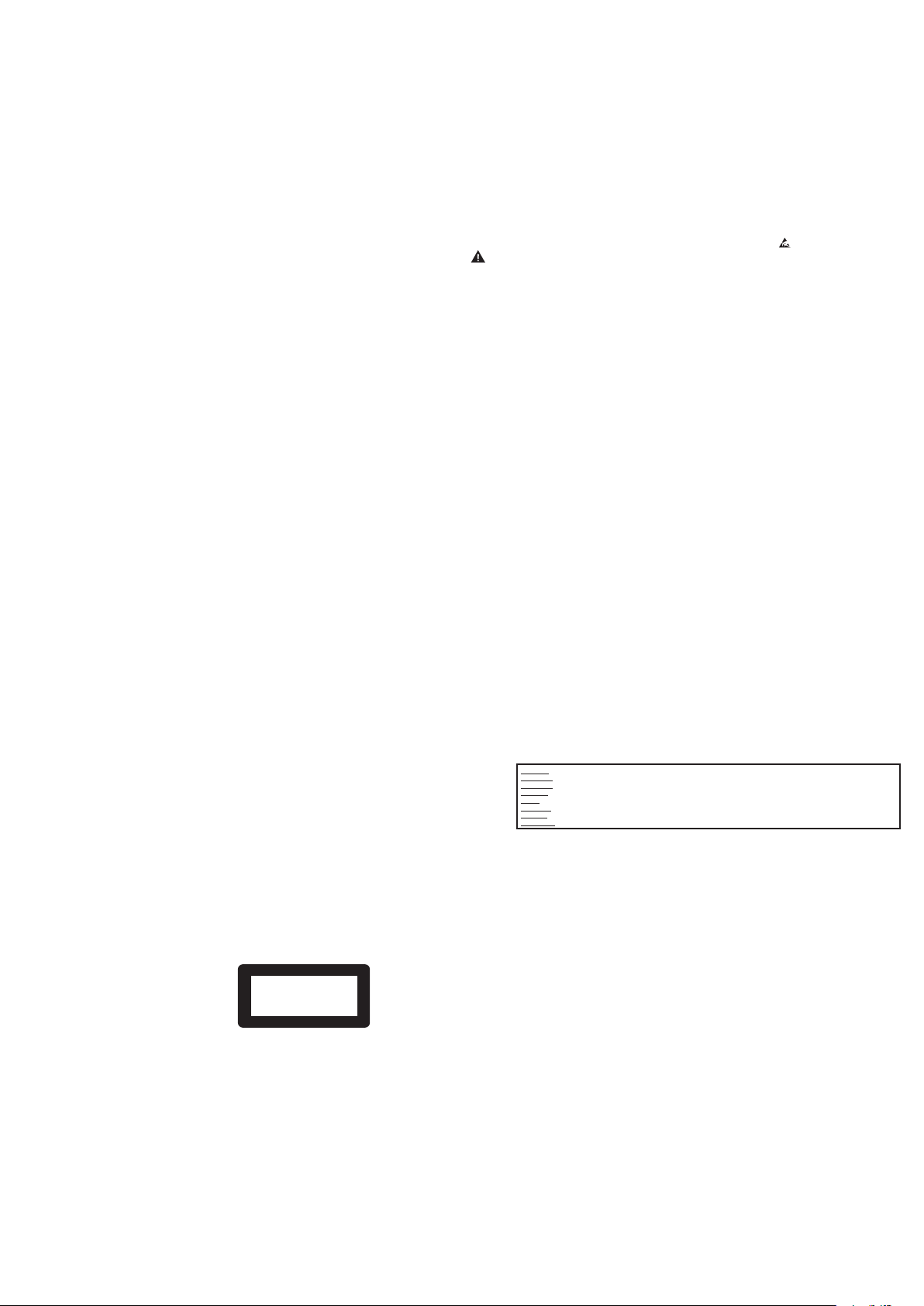
CLASS 1
LASER PRODUCT
2. Safety Information, General Notes & Lead Free Requirements
2.1 Safety Instructions
2.1.1 General Safety
Safety regulations require that during a repair:
• Connect the unit to the mains via an isolation transformer.
• Replace safety components, indicated by the symbol
only by components identical to the original ones. Any
other component substitution (other than original type)
may increase risk of fire or electrical shock hazard.
Safety regulations require that after a repair, you must return
the unit in its original condition. Pay, in particular, attention to
the following points:
• Route the wires/cables correctly, and fix them with the
mounted cable clamps.
• Check the insulation of the mains lead for external
damage.
• Check the electrical DC resistance between the mains
plug and the secondary side:
1. Unplug the mains cord, and connect a wire between
the two pins of the mains plug.
2. Set the mains switch to the ‘on’ position (keep the
mains cord unplugged!).
3. Measure the resistance value between the mains
plug and the front panel, controls, and chassis
bottom.
4. Repair or correct unit when the resistance
measurement is less than 1 MΩ.
5. Verify this, before you return the unit to the customer/
user (ref. UL-standard no. 1492).
6. Switch the unit ‘off’, and remove the wire between the
two pins of the mains plug.
2.1.2 Laser Safety
This unit employs a laser. Only qualified service personnel
may remove the cover, or attempt to service this device (due
to possible eye injury).
2.2 Warnings
2.2.1 General
• All ICs and many other semiconductors are susceptible
to electrostatic discharges (ESD,
during repair can reduce life drastically. Make sure that,
,
during repair, you are at the same potential as the mass
of the set by a wristband with resistance. Keep
components and tools at this same potential.
Available ESD protection equipment:
– Complete kit ESD3 (small tablemat, wristband,
connection box, extension cable and earth cable)
4822 310 10671.
– Wristband tester 4822 344 13999.
• Be careful during measurements in the live voltage
section. The primary side of the power supply, including
the heatsink, carries live mains voltage when you
connect the player to the mains (even when the
player is ‘off’!). It is possible to touch copper tracks and/
or components in this unshielded primary area, when
you service the player. Service personnel must take
precautions to prevent touching this area or components
in this area. A ‘lightning stroke’ and a stripe-marked
printing on the printed wiring board, indicate the primary
side of the power supply.
• Never replace modules, or components, while the unit is
‘on’.
2.2.2 Laser
• The use of optical instruments with this product, will
increase eye hazard.
• Only qualified service personnel may remove the cover or
attempt to service this device, due to possible eye injury.
• Repair handling should take place as much as possible
with a disc loaded inside the player.
• Text below is placed inside the unit, on the laser cover
shield:
). Careless handling
Laser Device Unit
Type : Semiconductor laser
GaAlAs
Wavelength : 650 nm (DVD)
: 780 nm (VCD/CD)
Output Power : 20 mW
(DVD+RW writing)
: 0.8 mW
(DVD reading)
: 0.3 mW
(VCD/CD reading)
Beam divergence : 60 degree
Figure 2-1
Note: Use of controls or adjustments or performance of
procedure other than those specified herein, may result in
hazardous radiation exposure. Avoid direct exposure to beam.
CAUTION VISIBLE AND INVISIBLE LASER RADIATION WHEN OPEN AVOID EXPOSURE TO BEAM
ADVARSEL
SYNLIG OG USYNLIG LASERSTRÅLING VED ÅBNING UNDGÅ UDSÆTTELSE FOR STRÅLING
ADVARSEL SYNLIG OG USYNLIG LASERSTRÅLING NÅR DEKSEL ÅPNES UNNGÅ EKSPONERING FOR STRÅLEN
VARNING SYNLIG OCH OSYNLIG LASERSTRÅLNING NÄR DENNA DEL ÄR ÖPPNAD BETRAKTA EJ STRÅLEN
VARO! AVATTAESSA OLET ALTTIINA NÄKYVÄLLE JA NÄKYMÄTTÖMÄLLE LASER SÄTEILYLLE. ÄLÄ KATSO SÄTEESEEN
VORSICHT SICHTBARE UND UNSICHTBARE LASERSTRAHLUNG WENN ABDECKUNG GEÖFFNET NICHT DEM STRAHL AUSSETSEN
DANGER VISIBLE AND INVISIBLE LASER RADIATION WHEN OPEN AVOID DIRECT EXPOSURE TO BEAM
ATTENTION RAYONNEMENT LASER VISIBLE ET INVISIBLE EN CAS D’OUVERTURE EXPOSITION DANGEREUSE AU FAISCEAU
Figure 2-2
2.3 Lead Free Requirement
Information about Lead-free produced sets
Philips CE is starting production of lead-free sets from
1.1.2005 onwards.
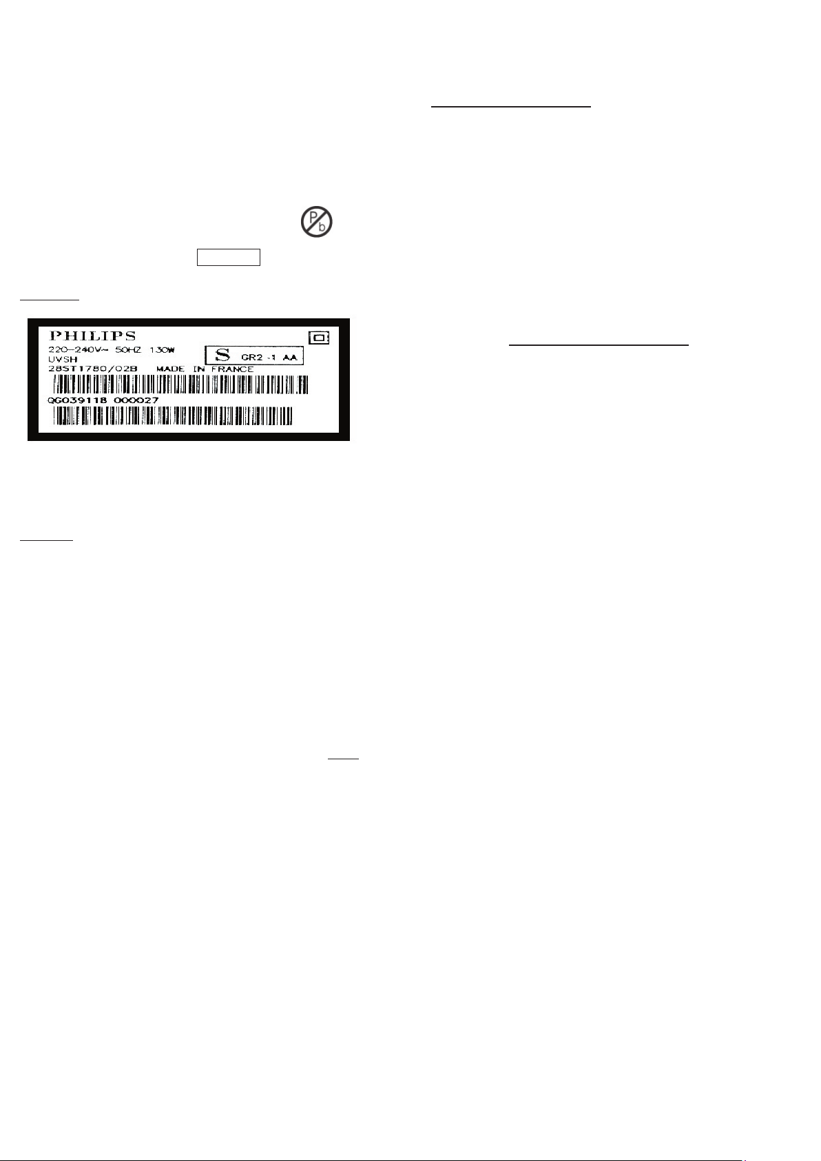
INDENTIFICATION:
Regardless of special logo (not always indicated)
One must treat all sets from
next rules.
Example S/N:
1 Jan 2005 onwards, according
• Special information for BGA-ICs:
- always use the 12nc-recognizable soldering temperature
profile of the specific BGA (for de-soldering always use the
lead-free temperature profile, in case of doubt)
- lead free BGA-ICs will be delivered in so-called ‘drypackaging’ (sealed pack including a silica gel pack) to
protect the IC against moisture. After opening, dependent
of MSL-level seen on indicator-label in the bag, the
BGA-IC possibly still has to be baked dry. (MSL=Moisture
Sensitivity Level). This will be communicated via AYSwebsite.
Do not re-use BGAs at all.
•
For sets produced before 1.1.2005 (except products of
2004), containing leaded solder-alloy and components,
all needed spare-parts will be available till the end of the
service-period. For repair of such sets nothing changes.
Bottom line of typeplate gives a 14-digit S/N. Digit 5&6 is the year, digit 7&8 is
the week number, so in this case 1991 wk 18
So from 0501 onwards = from 1 Jan 2005 onwards
Important note: In fact also products of year 2004 must be treated in this way as long as you
avoid mixing solder-alloys (leaded/ lead-free). So best to always use SAC305 and the higher
temperatures belong to this.
Due to lead-free technology some rules have to be respected by the
workshop during a repair:
• Use only lead-free solder alloy Philips SAC305 with order
code 0622 149 00106. If lead-free solder-pate is required,
please contact the manufacturer of your solder-equipment.
In general use of solder-paste within workshops should be
avoided because paste is not easy to store and to handle.
•
Use only adequate solder tools applicable for lead-free
solder alloy. The solder tool must be able
o To reach at least a solder-temperature of 400°C,
o To stabilize the adjusted temperature at the solder-tip
o To exchange solder-tips for different applications.
• Adjust your solder tool so that a temperature around 360°C
– 380°C is reached and stabilized at the solder joint.
Heating-time of the solder-joint should not exceed ~ 4 sec.
Avoid temperatures above 400°C otherwise wear-out of
tips will rise drastically and flux-fluid will be destroyed. To
avoid wear-out of tips switch off un-used equipment, or
reduce heat.
• Mix of lead-free solder alloy / parts with leaded solder alloy
/ parts is possible but PHILIPS recommends strongly to
avoid mixed solder alloy types (leaded and lead-free).
If one cannot avoid or does not know whether product is
lead-free, clean carefully the solder-joint from old solder
alloy and re-solder with new solder alloy (SAC305).
• Use only original spare-parts listed in the Service-Manuals.
Not listed standard-material (commodities) has to be
purchased at external companies.
•
On our website www.atyourservice.ce.Philips.com you
find more information to:
BGA-de-/soldering (+ baking instructions)
Heating-profiles of BGAs and other ICs used in Philips-sets
You will find this and more technical information within the
“magazine”, chapter “workshop news”.
For additional questions please contact your local repair-helpdesk.
1.Technical Specifications and Connection Facilities
V
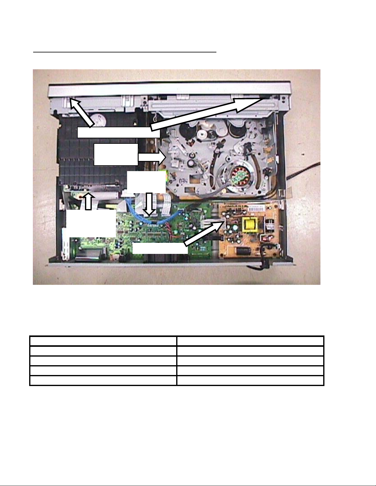
1.1 PCB Locations
Fronts Boards
HS Drive
Module
Analogue
Board
Digital Board
(below Basic
Engine)
PSU Board
1.2 Read / Write Speed
Type of Disc(Function) Disc Rotation Speed
Read Speed CD 7X CAV
Read Speed DVD 4X CAV
Write Speed DVD+R/RW 2.4X ZCAV
Write Speed DVD-R/RW 2X
1.3 General:
Mains voltage : 220V-240V
Mains frequency : 50Hz
Standby Power consumption : <3W

1.4 RF Tuner
Test Equipment :Fluke 54200 TV Signal generator
Test Stream:PAL BG Philips Standard test pattern
1.4.1.1 System:
PAL B/G, PAL D/K, SECAM L/L’, PAL I
1.4.1.2 RF – Loop Through
Frequency range : 43MHz-860MHz
Gain: (ANT IN-ANT OUT) : -4dB ± 2dB
1.4.1.3 Receiver:
PLL tuning with AFC for optimum reception
Frequency range : 45.25MHz - 857MHz
Sensitivity at 40dB S/N
(video unweighted) : ≤ 40dBµV at 75Ω
(high end)
≤ 60dBµV at 75Ω
(low end)
1.4.1.5 Video Performance:
Channel 25 / 503,25MHz,
Test pattern: PAL BG PHILIPS standard test pattern,
RF Level 74dBV
Measured on SCART 1
Frequency response : 0.1MHz - 4.00MHz ± 3dB
Group delay (0.1MHz-4.4MHz) : 0 nsec ± 150 nsec
1.4.1.6 Audio Performance:
Audio Performance Analogue – HiFi:
Frequency response at SCART 1
(L + R) output : 100Hz -12kHz / 0 ± 3dB
S/N Ratio (20Hz- 20KHz)
unweighted
Harmonic distortion
(1kHz, ± 25kHz deviation) :≤ 1.5%

Audio Performance NICAM:
Frequency response at SCART 1
(L + R) output : 40 Hz – 15 kHz / 0 ± 3dB
S/N according to DIN 45405,7,1967
and PHILIPS standard test pattern
video signal : ≥ 40dB
Harmonic distortion (1kHz) : ≤ 1.5%
1.4.1.7 Tuning
Automatic Search Tuning
scanning time without antenna : 3min. typical
stop level (vision carrier) : ≥ 37dBµV
Maximum tuning error(drift) during
operation : ± 100kHz
Tuning Principle
Automatic B, G, I, DK and L/L’ detection .Manual selection in “STORE” mode
1.5 Analogue Inputs / Outputs
1.5.1 SCART 1(Connected to TV)
Pin Signals:
1 - Audio-out R 1.8V RMS
2 - Audio-out R
3 - Audio-out L 1.8V RMS
4 - Audio GND
5 - Blue / Chroma GND
6 - Audio- in L
7 - Blue-out 0.7Vpp ± 0.1V into 75 W
8 - Function switch < 2V = TV
> 4.5V / < 7V = asp. Ratio 16:9 DVD
> 9.5V / < 12V = asp. Ratio 4:3 DVD
9 - Green GND
10 – P50 control not use
11 – Green out 0.7Vpp ± 0.1V into 75W (*)
12 - NC
13 - Red / Chroma GND
14 - Fast switch GND
15 - Red-out / Chroma-out 0.7Vpp ± 0.1V into 75W (*)
16 - Fast switch
RGB / CVBS or Y out < 0.4V into 75W = CVBS
>1V / < 3V into 75W = RGB

17 - Y/CVBS GND OUT
18 - CVBS GND IN
19 - CVBS-out 1Vpp ± 0.1V into 75W(*)
20 - CVBS-in
21 - Shield
1.5.2 SCART 2 (Connected to AUX)
Pin Signals:
1 - Audio-out R 1.8V RMS
2 - Audio-in R
3 - Audio-out L 1.8V RMS
4 - Audio GND
5 - Blue / Chroma GND
6 - Audio-in L
7 - Blue-in
8 - Function switch
9 - Green GND
10 - NC
11 - Green-in
12 - NC
13 - Red / Chroma GND
14 - Fast switch GND
15 - Red-in/Chroma-in
16 - Fast switch
RGB / CVBS or Y in
17 - CVBS-OUT GND
18 – Y/CVBS in GND
19 - CVBS out sync 1Vpp ± 0.1V into 75Ω
20 – CVBS in / Y-in
21 – Shield
1.5.3 Audio/Video Front Input Connectors
Audio – Cinch
Input voltage : 2.2Vrms
Input impedance : > 10kΩ
Video – Cinch
Input voltage : 1Vpp ± 3dB
Input impedance : 75Ω
Video – YC (Hosiden)
According to IEC 933-5

Superimposed DC-level on pin 4(load >100kΩ)
<2.4V is detected as 4:3 aspect ratio
>3.5V is detected as 16:9 aspect ratio
Input voltage Y : 1Vpp ± 3dB
Input impedance Y : 75Ω
Input voltage C : 300 mVpp ± 3dB
Input impedance C : 75Ω
1.6 Digital Inputs / Outputs
1.6.1 Digital Output
Digital Audio – Coaxial
LCM : according IEC 60958
MPEG 1,MPEG2,AC3 : according IEC 61937
DTS : according IEC 61937+addendum
1.7.3 Digital Video Input(IEEE 1394)
Implementation Standard according:
IEEE Std 1394-1995
IEC61883 - Part1
IEC61883 - Part2 SD-DVCR (02-01-1997)
Specification of consumer use digital VCR’s using 6.3mm magnetic tape – dec.
1994
Mechanical connection according to Annex of IEC 61883-1
1.8 Video Performance
All outputs loaded with 75 Ω
SNR measurements over full bandwidth without weighting.
1.8.1 SCART (RGB)
SNR : > -65dB on all output
Bandwidth : 4.8MHz ± 2dB
1.9 Audio Performance CD
1.9.1 Cinch Output Rear
Output voltage 2 channel mode : 2Vrms ± 2dB
Channel unbalance (1kHz) : < 0.22dB

Crosstalk 1kHz : > 100dB
Crosstalk 16Hz-20kHz : > 87dB
Frequency response 20Hz-20kHz : ± 0.5dB max
Signal to noise ratio : < 85dB
Dynamic range 1kHz : <83dB
Distortion and noise 1kHz : < 83dB
Distortion and noise 16Hz-20kHz : < 75dB
Intermodulation distortion : < 70dB
Mute : < 95dB
1.9.2 Scart Audio
Output voltage 2 channel mode : 1.6Vrms ± 2dB
Channel unbalance (1kHz) : < 1dB
Crosstalk 1kHz : > 85dB
Crosstalk 16Hz-20kHz : > 70dB
Frequency response 20Hz-20kHz : ± 0.5dB max
Signal to noise ratio : > 80dB
Dynamic range 1kHz : > 75dB
Distortion and noise 1kHz : > 75dB
Distortion and noise 16Hz-20kHz : > 50dB
Intermodulation distortion : > 70dB
Mute : > 80dB
1.10 Dimensions and Weight
Height of feet : 5.5mm
Apparatus(WxDxH) : 435 x 100 x 344mm
Weight without packaging : 5.2kg
Weight with packaging : 7.0kg
1.11 Laser Output Power & Wavelength
1.11.1 DVD
Output power during reading : 0.8mW
Output power during writing : 20mW
Wavelength 650nm
1.11.2 CD
Output power :0.3mW
Wavelength :780nm

1.2 VHS Drive Technical Specifications
1.2.1 Servo
1.2.1.1 Drum lock Phase Changing Time :6.5H
1.2.1.2 WOW Flutter R/P(CCIR WTD) :0.3%
1.2.1.3 Jitter :0.07µs
1.2.2 Video
1.2.2.1 Output Level(R/P EBU Full Color Bar) at 75Ω :1.0Vpp
1.2.2.2 Resolution (R/P monochronous scope W/O burst:230 line
1.2.2.3 Signal to Noise Ratio(Y-Band) :43dB
1.2.2.4 (C AM) :41dB
1.2.2.5 (C PM) :38dB
1.2.3 Normal Audio
1.2.3.1 Output Level(R/P Input 1KHz – 10dBv) :-5dBµv
1.2.3.2 S/N :40dB
1.2.3.4 Distortion ratio :1.5%
1.2.3.5 Frequency Response( at reference 1KHz,-20dBv)
At 200Hz :-3dB
At 6KHz :-3dB
1.2.4 HiFi AUDIO
1.2.4.1 Output Level :-9dBv
1.2.4.2 Dynamic range(R/P JIS A) :80dB
1.2.4.3 Frequency Response(at reference R/P Input 1KHz –20dBv)
1.2.4.4 At 20Hz :0dB
Frequency Response(at reference R/P Input 1KHz –20dBv)
At 20KHz :0dB
1.2.4.5 Distortion (at reference R/P Input 1KHz –10dBv)
:0.5%

Manual Procedure to remove the tape from the loader
Immediate action must be done to remove the Video Cassette on the set manually as described belo w :
Note : Item number refers to the Deck Parts List in VCR Module
(12NC:2422 549 01124) unless otherwise stated
1. Turn the B525 (LDG Belt MK11 ) in the direction
indicated by the arrow below in figure 1:
B525
Figure 1:Turning B525 by hand
2. Upon hearing the click sound , the Clip[B587] holding the VCR will be released as shown in figure 2.
Figure 2:Clip 587 released
3.The tape will be slackened as shown in figure 3.
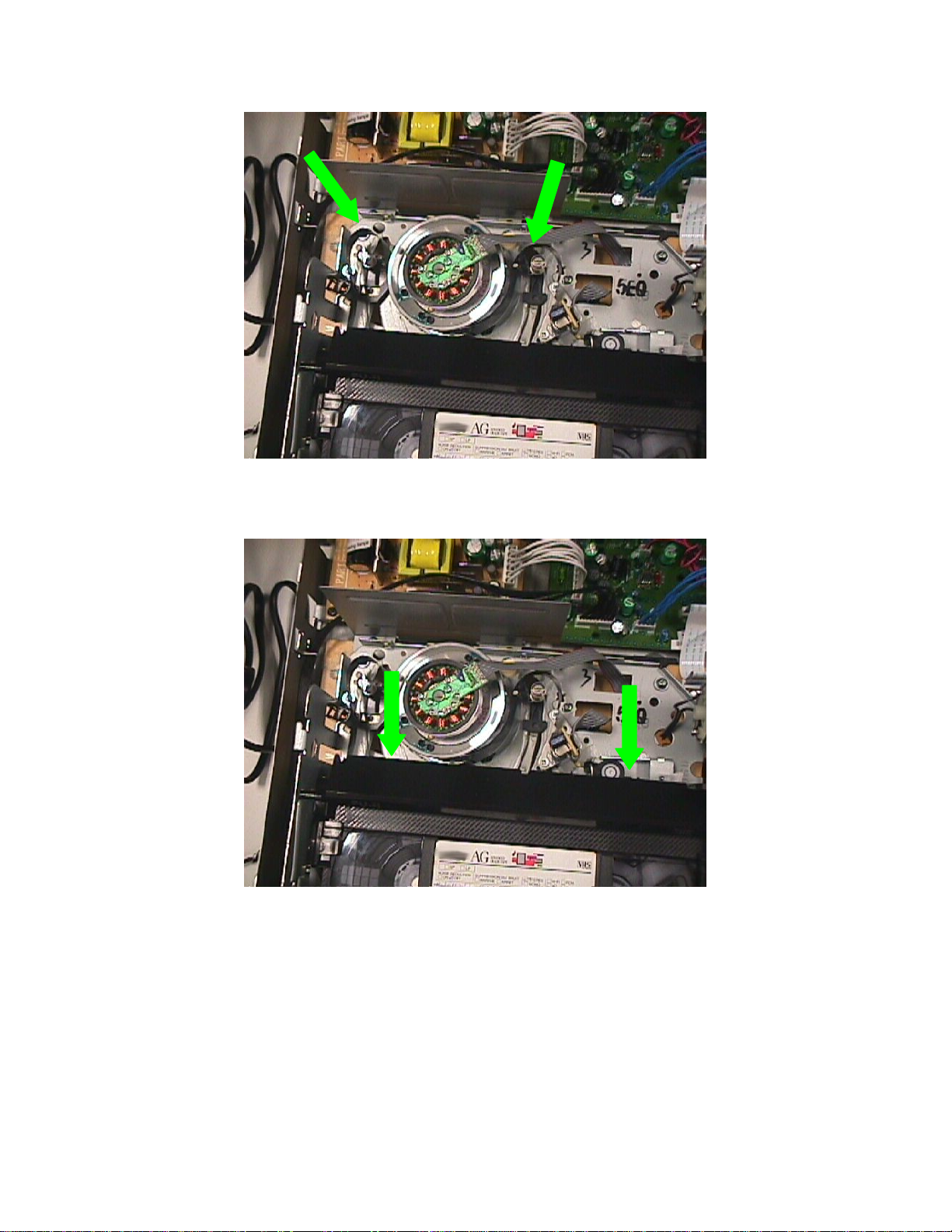
Figure 3:Tape slackened
4.The video casette slowly reversed and raised to loading position in figure 4 .
Figure 4 :Video Casette Slowly reversed
5. Fold the slack of the video by hand to minimize damage by the front dust cover
cover upon approaching the B354 & B355 position will be closed and comes out of the Door Flap(112 of
exploded view of DVDR3430V)
of Videocasette.The front
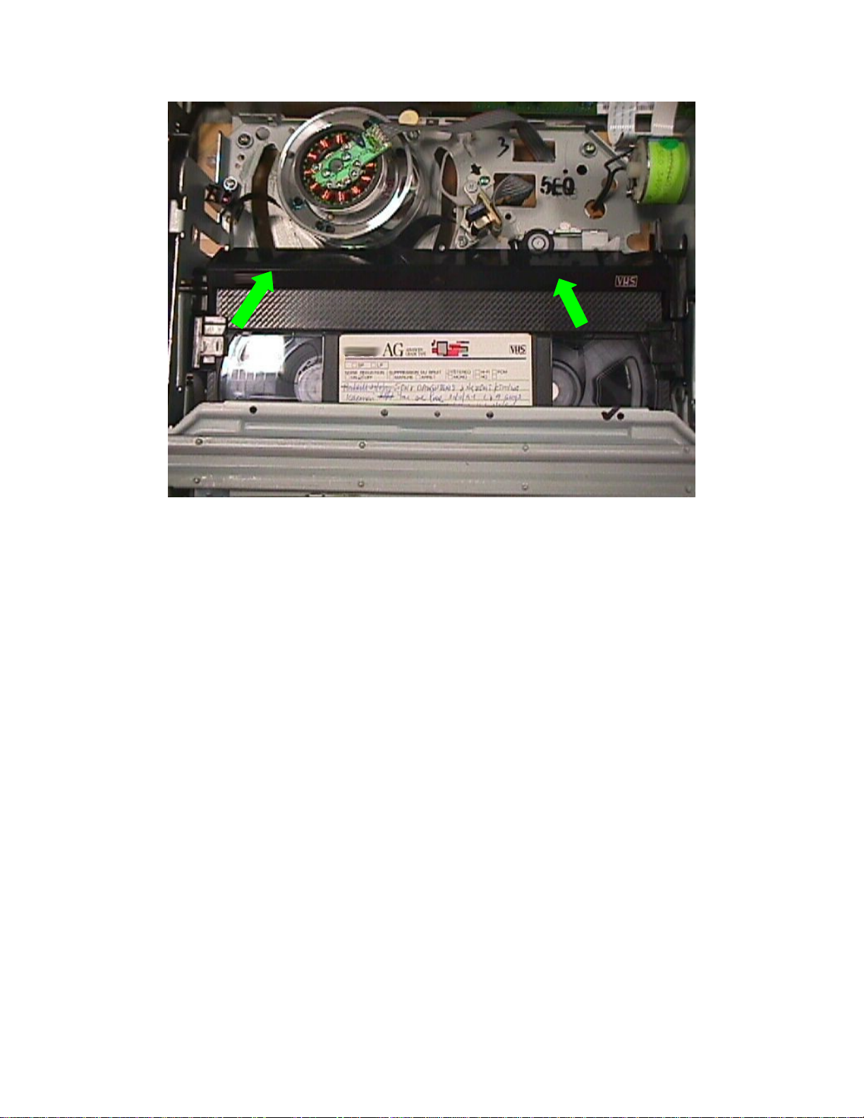
Figure 5:The dust cover slowy cover the tape due to spring action
of the dust cover
6.Remove the cassette as you normally does from the front loading position
.

Mechanical Instructions
Note : The position numbers given here refers to the Exploded view
1.1 Dismantling of the DVD Tray Cover manually
1) Insert a screw-driver into the slot provided at the bottom of the set and
push in the direction as shown in figure 1 to unlock before sliding the Tray Cover 110
out.
Figure 1:Unlock DVD tray
1.2 Dismantling of the Basic Engine (Drive D4.5)
1) Remove 8 screws to loosen Top cover 240 .
2) Remove 4 screws to loosen the Basic Engine Holder D4.5
As shown in Figure 2.

Figure 2- Remove Basic Engine mounting
3) Remove 4 screw to detach the Holder from the Basic Engine and unscrew the Heatsin k
plate .
Basic Engine Service position as show once heatsink plate removed in Figure 4-4.
Remove the
Heatsink plate
Figure 3 – Basic Engine Service Position
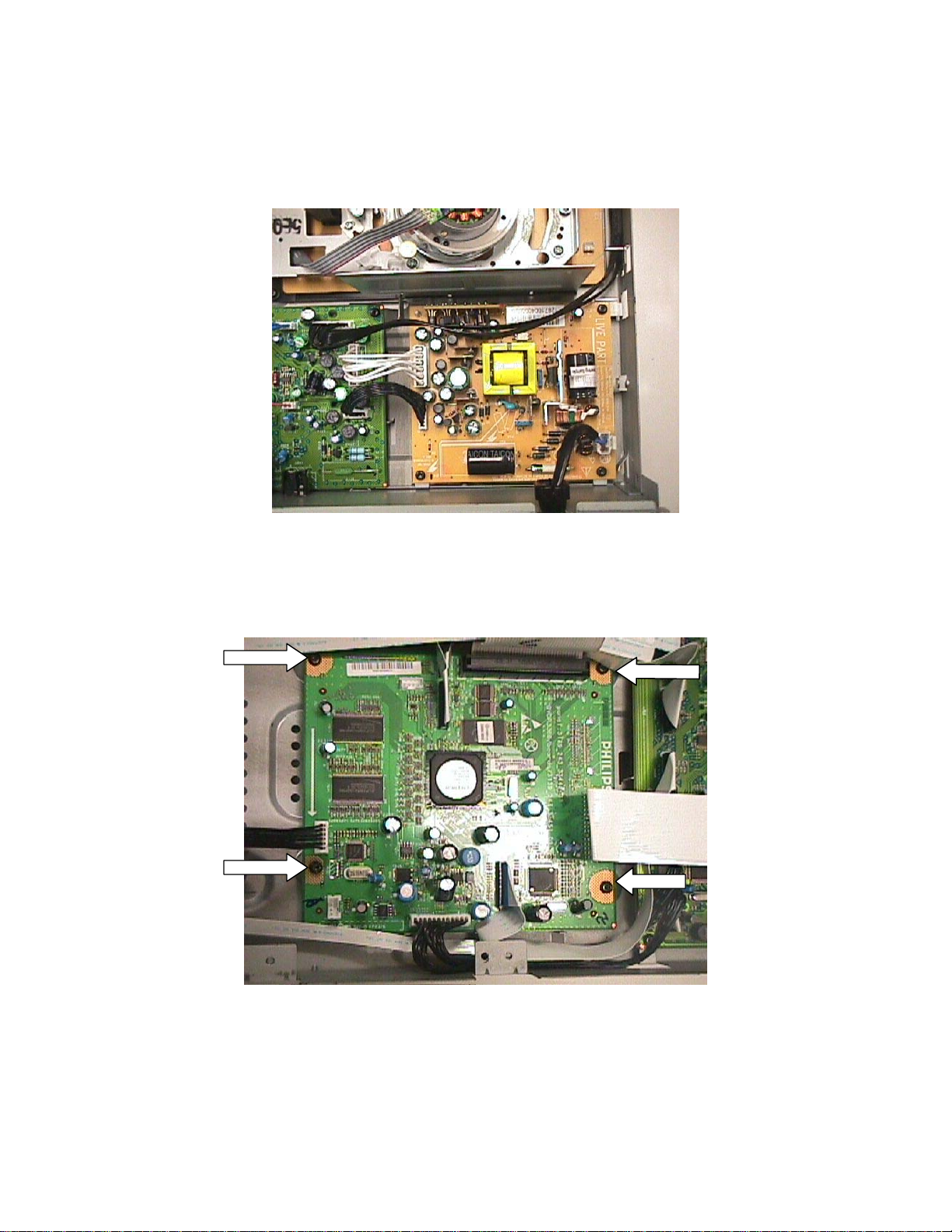
1.3 Dismantling of the PSU Board
4) Remove 4 screws to loosen the PSU Board 1007 as shown in Figure …
5) Service position for PSU Board is given in Figure 8.
Figure 4 – Remove PSU mounting
1.5 Dismantling of the Digital Board
Remove 4 screws to loosen the Digital Board 1004 as shown in Figure 4-5.
Figure 5 :Remove Digital Board Mounting
1) Service Position for Digital Board is given in Figure 6.
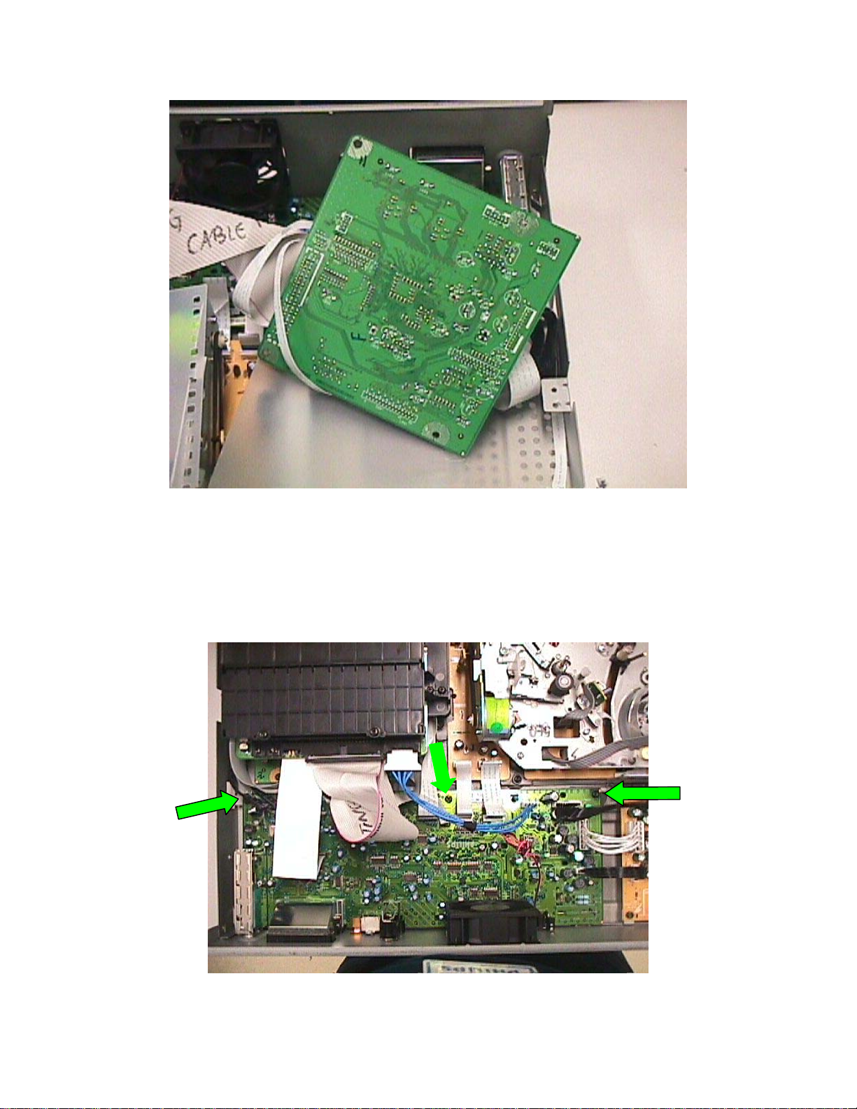
Figure 6: Digital Board Service Position
1.5 Dismantling of the Analogue Board
1) Remove screws from the rear panel 230 to detach Analogue Board shown
in Figure 7.
2) Service Position of Analogue Board is given in Figure 8.
Figure 7:Detach Analogue Board

Figure 8 :Analogue Board Service Position
Insulation sheet
1.6 Dismantling of the VHS Drive Module
Note:For items name& number mentioned below , please refer to VCR
Module HK100ED (12NC:2422 549 01124)
1) Detach VHS Drive Module by unscrewing 5 screw shown on Figure 9
Figure 9:Remove VHS Module
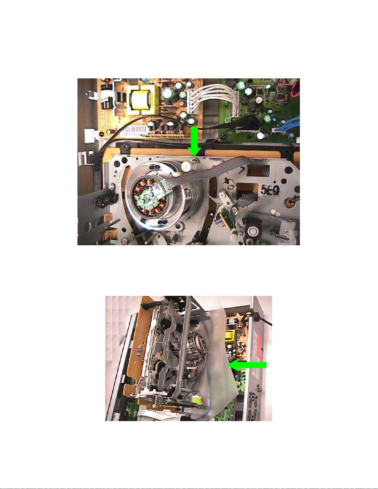
2) While unscrewing the cross screws , great care must be taken with the
screw located near the helical drum at the VHS module to prevent
accidental scratches to the drum shown in figure 10.
Figure 10:Caution area
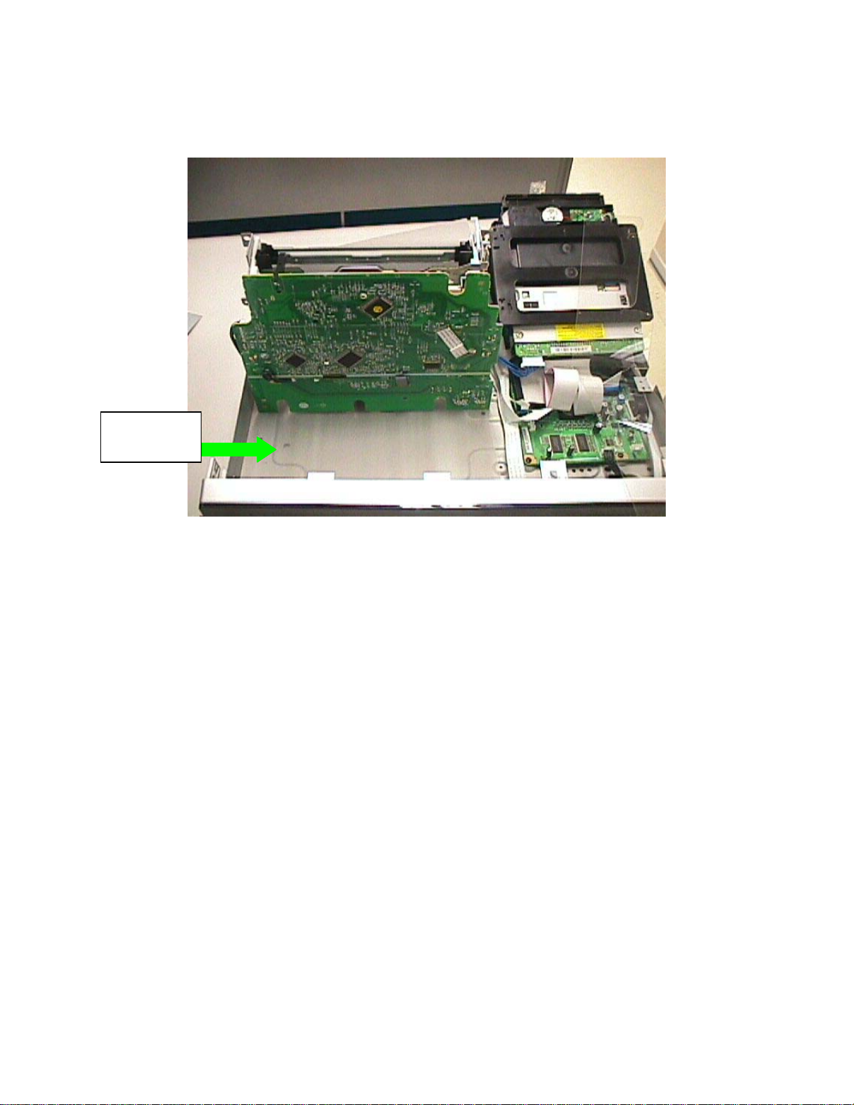
3) Make the VCR module upright and Insulation sheet must be inserted onto
the drum to prevent damage by contact to the Recorder frame shown in
Figure 11.
Insulation Sheet
Figure 11:Insulation sheet for precaution
Service Position of the VCR module is given in Figure 12.
Insulation
Sheet
Figure 12:Service Position of the VHS Drive Module

Firmware Upgrading
A. Preparation to upgrade firmware:
1. Unzip the zip-archive file
2. Copy the files into different folder for burning into separate CD-R/CDRW.
3. Start the CD Burning software and create a new CD project (data disc) with the following settings:
File system: Joliet
Format: MODE 2: CDROM XA
Recording mode: SINGLE SESSION (TRACK-AT-ONCE), FINALIZED CD
Note: Long file name is necessary for the preparation of the upgrade disc
4. Place the file into the root directory of the new CD project.
5. Burn the data onto blank CDR or CD-RW.
B. Procedure to apply the Drive upgrade:
1. Open the tray and load the Upgrade CDROM .
2. The tray closes and set will display:
“DRV UPG”
3. The OSD will display
“Loader Software Upgrade
Software Upgrade Disc detected . Select OK to start upgrading or CANCEL to exit.”
4. Click on the OK button .
5. The set will display:
“DRIVE UPGRADING”
With the OSD display
“Upgrading Software .Please Wait.Do not switch off the power.”
The whole process takes less than 5 minutes
6. When the upgrade is completed the tray will open automatically and the set will display:
“Loader Upgrade process has completed successfully .Press <OK> to reboot system.”
7. The tray open and the set will display:
8. The tray will display:
9. The OSD will display
10. Click on the OK button .
11. The set will display :
“DRV OK”
“SW UPGD”
“Software Upgrade Disc detected.Select OK to start upgrading or CANCEL to exit .”

“Upgrading SW”
12. And the OSD will display
“Upgrading Software .Please Wait.Do not switch off the power.”
The whole process takes less than 5 minutes
13. When the upgrade is completed the tray will open automatically and the set will display:
“System is successfully upgraded.Remove disc from tray and reset system.”
14. The tray open and the set will display:
“SW DONE”
15. Press <OK> and the set goes to standby .
B. How to read out the firmware version to confirm set has been upgraded:
1. Power up the set
2. Ensure no disc inside the loader,if no ,open the tray to remove the disc and close the tray.
3. Press <0> <0> <0><9> in succession
4. Press <OK> button
5. The TV connected to the set will display:
“DVDR3430V_EU_V04_02 , Region :2 , Drive 45.04.05
Build: 0097_PHILIPS_V03 JAN 11 2006 , 09:28:29 Stroke:31 ”
and the tray will open automatically for user to remove CD-ROM.
Note: Do not press any buttons or interrupt the mains supply during the upgrading
process, otherwise the set may becomes defective.
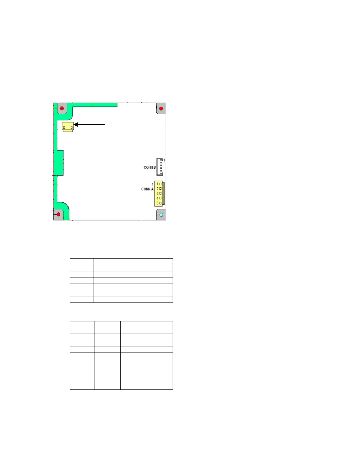
1.1 PSU Board
1.1.1General
Mains
Connection
The PSU board provides the following connection to the rest of the set:
• Connector A(Connector J1 on Analogue Board): Supply/Signal to Analog Board Conn. 1101
• Serve as supply to Digital Board
Pin
1
2
3
4
5
• Connector B(Connector J2 on Analogue Board): Supply/Signal to Analogue Board Conn. 1102
Pin Supply/
1 VGN
2 5N
3 GND
4 IPFAIL
5 GND
6 12V
Supply/
Signal
12V
GND
5V
3.3V
GND
Signal
Remarks
Remarks
HIGH>4.0v =
power good
LOW<0.5v =power
fail

The Mains must be disconnected from the Set before attempting the procedure mentioned
below:
The PSU is designed with short-circuit protection that will shutdown the power supply. When this
happen, the voltage stored in capacitor C1 and C40 will prevent the Pow er Su pply to turn-on,
therefore they must be discharged with a screwdriver with high electrical isol ation handle before the
PSU can function normally again.
Note :During the process of discharging the capacito rs ,spark can be observed which is typical of
the high voltage stored in Capacitor C1 and C40.

1.2 Front Board (Panel – Display + Key)
1.2.1 General
This board consists of the following parts:
• Slave µP
• Frontend (Audio & Video)
• VFD Heater voltage Generator
1.2.2 FIP Control Driver (IC 7105 : UPD16316GB)
The core element of the Front Display + Key board is the slave µP.
It runs on a 5V supply and is responsible for the following functions:
• Interface with the Domino chip on the Digital Board
• Evaluation of the keyboard matrix within Front board
• Decoding the remote control commands from the infra-red receiver
• Activation and control of the display
• Timer Wake-up activation
It runs on two clock frequencies namely:
• 5MHz for normal operation
• 32.768KHz for the real time clock
1.2.3 Interface to the Domino chip
It communicates with the Domino Host on the Digital board via a 6-wire synchonous serial interface. The Host
is always the master to generate the communication clock to the slave µP irrespective of the direction of data
transfer.
1.2.4 Evaluation of the keyboard matrix
A key matrix is used on the Front board. The FIP control driver does the key-scanning with FIP9 - FIP24 (pin
23-26 and 29-40) as output and KEY_A - KEY_C (pin 41-43) as input. Each key is assigned a key code based
on the output and input ports, and the slave µP will do the evaluation by getting the key codes.
1.2.5 IR receiver and signal evaluation
The IR receiver on the Front Board contains a selectively controlled amplifier as well as a photodiode. The
photo-diode changes the received infrared transmission to electrical pulses, which are then amplified and
demodulated. On the output of the IR receiver, a pulse sequence with TTL-level, which corresponds to the
envelope curve of the received IR remote control command, can be measured. This pulse sequence is fed into
the slave µP for further processing via pin 13.
1.2.6 Vacuum Fluorescent Display [1002 : HUV-08SS65T]
The VFD is fully controlled and driven by the FIP control driver.
1.2.7 VFD Heater Voltage Generator
The oscillator circuit provided by [5100, 2101, 2102 & 7100] provides the necessary sine wave signal for
transistors [7101, 7102 & 7103] to generate the 50% duty-cycle 48KHz AC square-wave signal for the filament
of the VFD.
1.2.8 Timer Wake-up activation
During the Standby mode, the FIP ctrl driver provides a wakeup call (POWER_CTL-line switches to high) to the
Domino Host on the Digital Board. It will then starts up and asks for the wake-up reason.
1.3 Analog Board
1.3.1 General

The pc board consists of the following parts:
• Fan Control (optional)
• Power Supply Unit
• Tuner Frontend
• Audio ADC/DAC
1.3.2 Power Supply Unit Interface
This power supply unit Interfacing interfaces with a external power supply board ,draws the required voltage
level to the various supply lines to the requirement mentioned below:
The following are the various supply lines provided:
• 3V3SW to CU, DAC_ADC, Digital Board
• 5V to IOA, IOV, CU, CINCH, MSP, DIGIO and FV
• 5N to MSP (provision only) and Digital Board (provision only)
• 5VE to Basic Engine
• 5V_BE to Digital Board
• 5NSTBY to IOA, CINCH and DAC_ADC
• 5VSTBY to IOA, IOV, FV, MSP, DAC_ADC, Front Board
• 8VSTBY to MSP
• 12V to Digital Board,VCR module
• 12VSTBY to CU, IOV, DAC_ADC, Front Board
• 12VE to Basic Engine and Digital Board (provision only)
• 33VSTBY to FV
• VGNSTBY to Front Board
• 21V to VCR module loader motor
Standby modes:
In Standby mode the STBY control line is low, switching off the 3V3SW, 5V, 5N (provision), 5VE, 12V and 12VE
supply and thus reducing the power consumption.
1.3.3 Tuner Frontend [1151 : TMQZ2]
It has a RF IN for antenna connection and RF OUT which provides a RF loop through for connection to the TV.
The Frontend ( Tuner & IF-demodulator ) is controlled by I
Domino Host on the Digital board.
Complete video processing is done in this unit and the video output (CVBS) is taken out from the [VIDEO_OUT]
pin 13 via a transistor as CVBS_TV-line to the Video I/O circuitry. The audio-IF component SIF1 is taken out
from the [SIFOUT] pin 10 for the demodulation by the Multi-sound processor (MSP).
1.3.4 Audio demodulator
The sound demodulation is done by the MSP3415 [7315], which is also fully controlled via I
Domino Host. The audio signals are available at pin 26 and pin 27 and fed as AFER- & AFEL- line to the audio
I/O for further processing.
Audio Routing
2
C (SCL_5V- and SDA_5V-) lines coming from the
2
C bus by the
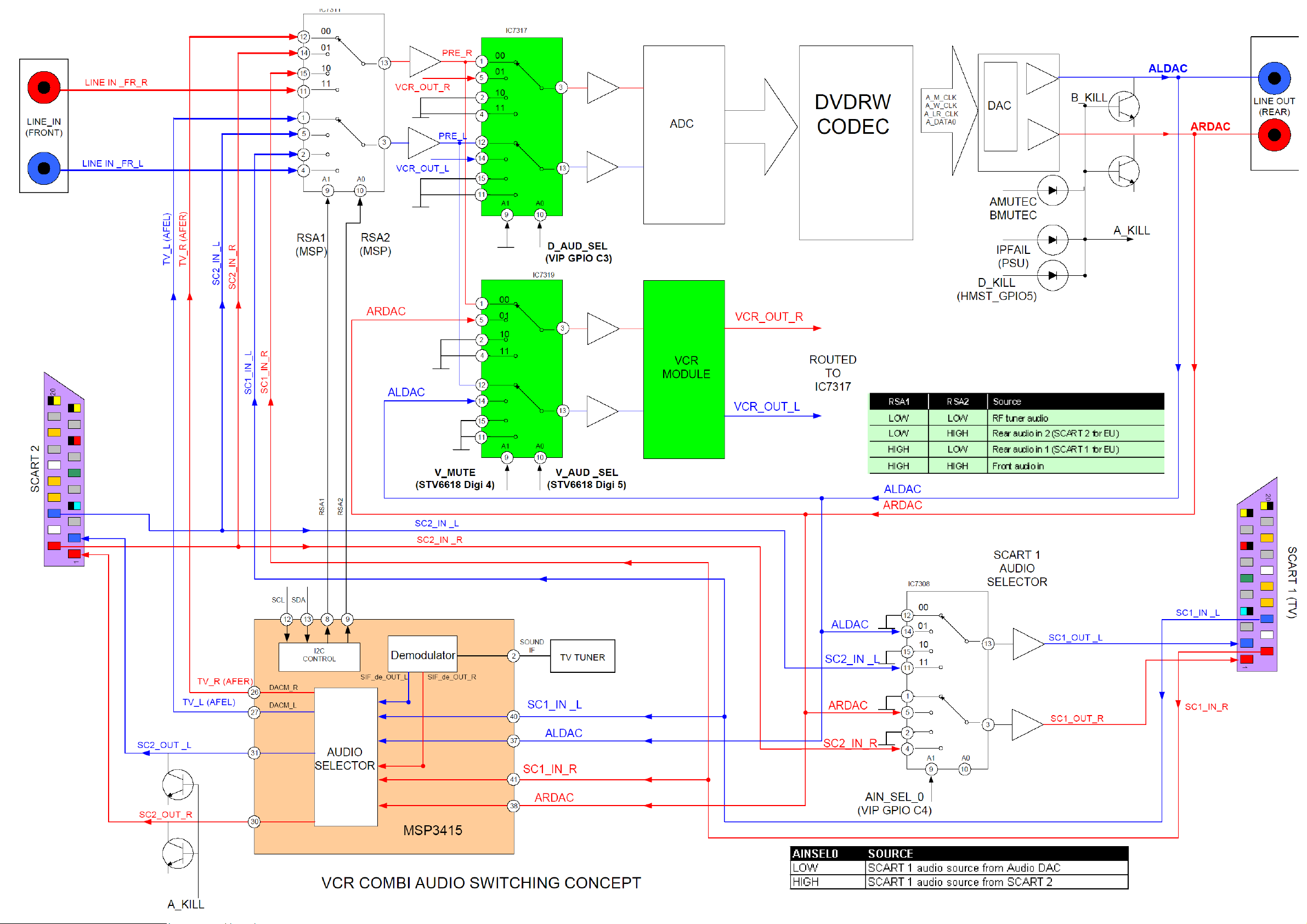

1.3.5 Audio routing
The sound processing is always done in stereo (that means separate left- and right- channel) and the complete
switching is realized by using HEF4052 which is a dual four-to-one multiplexer and MSP3415G which is a multisound processor.
a) Scart 1 – Output path
The multiplexer [7311] selects either signals from the Scart 2 Input (AIN2L/AIN2R) or the Audio DAC
(ALDAC/ARDAC) as the output source for Scart 1 (AOUT1L/AOUT1R).
b) Scart 2 – Output path
The MSP [7315] selects either signals from the Scart 1 Input (AIN1L/AIN1R), the Audio DAC (ALDAC/ARDAC)
or the Tuner Frontend as the output source for Scart 2 (AOUT2L/AOUT2R).
c) Record path (DVDR Recording )
The record-selector [7311] selects either signals from the Scart 1 Input (AIN1L/AIN1R), Scart 2 Input
(AIN2L/AIN2R), Front Cinch (AINFL/AINFR) or the MSP (AFEL/AFER) and routes to the audio ADC
(ALADC/ARADC) for record purposes. The switch is controlled via RSA1 and RSA2 signals coming from the
MSP.
d) Record path (VCR Recording )
Another record-selector Multiplexer HEF4052B [7319] , selects either audio signal from left (ALDAC) and right
(ARDAC) (from DVDRW), with PRE_R and PRE_L audio signal (from all external source other than DVDRW)
and routes to VCR for record purposes . The switch is controlled via V_AUD_SEL and V_AUD_MUTE signals
coming from the STV6618 matrix.
1.3.6 Audio ADC/DAC
The conversion of analog audio signals from the record-selector [7311] outputs (ALADC/ARADC) is done via
UDA1361TS [7704]. This IC can process input signals up to 2V
input pins. All required clock signals are generated on the digital board and only the audio data (A_DAT-line)
are routed to Digital board for further processing.
The transformation of digital audio back into analog domain is done by CS4351 [7411]. All necessary clock
signals are coming from the digital board and digital audio data (D_DATA0-line) are converted into analog
signals (pin 15 and 18). The output signals from the audio DAC part (ALDAC/ARDAC) are directly routed to the
rear cinch sockets. To avoid plops and any other audible noise on the output muting circuits are implemented
for each channel.Muting for the various other output lines are done via AKILL & BKILL-lines which is a
combination of the D_KILL from the Digital board and POWER_FAIL from power supply and AMUTE & BMUTE
(digital silence mute) from DAC-part.
VIDEO ROUTING OF DVDR3430V
by using external resistors in series to the
rms

 Loading...