Philips DVDR-3408 Service Manual
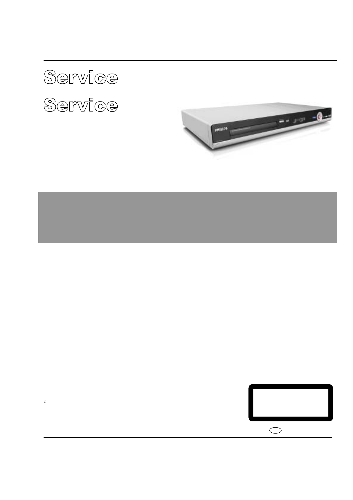
DVD Recorder DVDR3408
DVDR3408/93
Service
Service Manual
TABLE OF CONTENTS
Page
C
Copyright 2006Philips Consumer Electronics B.V. Eindhoven, The Netherlands
All rights reserved. No part of this publication may be reproduced, stored in aretrieval system or
transmitted, in any form or by any means, electronic, mechanical, photocopying, or otherwise
without the prior permission of Philips.
3139 785 32350
Published by TCL-KC 0638Service Audio Printed in The Netherlands Subject to modification
Version 1.0
. Technical Specifications………………………………………….......1-2
. Safety Instruction, Warning & Notes………...…………….………...1-3
. Mechanical and Dismantling Instructions…………………..............2-1
. Region Code, Software Version & Upgrades……………………….3-1
. Trouble Shooting Chart………………………………………………..4-1
. Block and Wiring Diagram…………………………………….…...….5-1
. Electrical Diagrams and Print-layouts……………………….……….6-1
. Set Mechanical Exploded View & Parts List………………………...7-1
. Electrical Parts List…………………………………………..........…..8-1
. Revision List……………………………………………………...........9-1
PHILIPS
CLASS 1
LASER PRODUCT
GB

Technical Specifications
1-2
Video Recording
Recording System: PAL / NTSC
Compression formats: MPEG2
Modes of Record Quality
High Quality: HQ
Standard Play: SP
Standard Play Plus: SP+
Long Play: LP
Extended Play: EP
Super Long Play: SLP
Super Extended Play: SEP
Audio compression: Dolby Digital
Video Playback
Disc Playback Media: CD, CD-R / -RW, DVD, DVD-Video,
DVD+R, DVD+RW, DVD-R, DVD-RW, SVCD, Video CD,
Compression formats: MPEG2, MPEG1, DivX
Video Disc Playback System: PAL, NTSC
Audio Playback
Disc Playback Media: CD, CD-R / -RW, MP3-CD,MP3-DVD,
WMA
Compression formats: Dolby Digital, MP3, MPEG2 Multichannel,
PCM
MP3 Bit Rates: 32~256Kbps and VBR
Still Picture Playback
Disc formats: DVD+R/+RW, DVD-R/-RW, Picture CD
Picture compression format: JPEG
Picture enhancement: Rotate
Picture/ Display
Aspect ratio: 4: 3, 16: 9
D/A Converter: 10Bit, 54MHz
A/D Converter: 10Bit, 27MHz
Picture Enhancement: Progressive Scan
Audio Performance
D/A Converter 24Bit, 96KHz
A/D converter 24Bit, 96KHz
Signal / Noise (1KHz) 90dB
Dynamic range (1KHz) 80dB
Crosstalk (1KHz) 80dB
Turner/Reception/ Transmission
Receive TV Signal: PAL
Aerial Input: 75 ohm coaxial (IEC75)
Storage Media
Recording media: DVD+R/-R, DVD+RW/-RW, DVD+R DL,
Recording speed: 2.4X
Connectivity
Rear Connections
- S-video Out
- Video (CVBS) Out
- Audio left/right Out
- Digital audio out (coaxial)
- RF antenna in
- RF TV out /Y,Pb,Pr out
- S-Video in
- Video (CVBS) in
- Audio left/right/ in
Front Connections
- I.LINK DV in (IEEE 1394 4-pin)
- Video in
- Audio left/right / in
Convenience
Programming / Timer Enhancements:
Daily / Weekly, Repeat Program, Manual Timer,
One Touch Recording
Timer recording events: 20
Power
Power Supply: 110~240 V; 50~60 Hz
Power Consumption: 28 W
Standby power consumption: < 4.0W
Dimensions :
Set Dimensions (W X H X D): 427 X 48 X 318mm
Net Weight : 3.18 Kg
Specifications subject to change without prior notice.

g &
Safety instruction, Warnin
Safety instructions
1. General safety
Safety regulations require that during a repair:
. Connect the unit to the mains via an isolation
transformer.
. Replace safety components indicated by the symbol
, only by components identical to the original ones.
Any other component substitution (other than original
type) may increase risk of fire or electrical shock
hazard.
Safety regulations require that after a repair, you must
return the unit in its original condition. Pay, in particular,
attention to the following points:
. Route the wires/cables correctly, and fix them with
the mounted cable clamps.
. Check the insulation of the mains lead for external
damage.
. Check the electrical DC resistance between the
mains plug and the secondary side:
1) Unplug the mains cord, and connect a wire
between the two pins of the mains plug.
2) Set the mains switch the “on” position (keep
the mains cord unplug).
3) Measure the resistance value between the
mains plug and the front panel, controls, and
chassis bottom.
4) Repair or correct unit when the resistance
measurement is less than 1M
5) Verify this, before you return the unit to the
customer/user (ref. UL-standard no. 1492).
6) Switch the unit “off”, and remove the wire
between the two pins of the mains plug.
Ω
.
Notes
1-3
2.Laser safety
This unit employs a laser. Only qualified service personnel may
remove the cover, or attempt to service this device (due to
possible eye injury).
Laser device unit
Type : Semiconductor laser
: InGaAIP (DVD)
: AIGaAs (CD)
Wavelength : 658nm (DVD)
: 783nm (CD)
Power out objective lens: 1.0mW (DVD read)
: 1.2mW (CD read)
Note: Use of controls or adjustments or performance of
procedure other than those specified herein, may result in
hazardous radiation exposure. Avoid direct exposure to beam.

A
A
A
A
1-4
Warning
1.General
. All ICs and many other semiconductors are
susceptible to electrostatic discharges (ESD).
Careless handing during repair can reduce life
drastically. Make sure that, during repair, you are at
the same potential as the mass of the set by a
wristband with resistance. Keep components and tools
at this same potential. Available ESD protection
equipment:
1) Complete kit ESD3 (small tablemat, wristband,
connection box, extension cable and earth cable)
4822 310 10671.
2) Wristband tester 4822 344 13999.
. Be careful during measurements in the live voltage
section. The primary side of the power supply ,
including the heat sink, carries live mains voltage
when you connect the player to the mains (even when
the player is “off”!). It is possible to touch copper tracks
and/or components in this unshielded primary area,
when you service the player. Service personnel must
take precautions to prevent touching this area or
components in this area. A “lighting stroke” and a
stripe-marked printing on the printed wiring board,
indicate the primary side of the power supply.
. Never replace modules, or components, while the
unit is “on”.
2. Laser
. The use of optical instruments with this product will increase eye
hazard.
. Only qualified service personnel may remove the cover or
attempt to service this device, due to possible eye injury.
. Repair handing should take place as much as possible with a
disc loaded inside the player.
. Text below is placed inside the unit, on the laser cover shield:
CAUTION: VISIBLE AND INVISIBLE LASER RADIATION WHEN OPEN
VOID EXPOSURE TO BEAM.
DVARSEL: SYNLIG OG USYNLIG LASERETRALING VED ABNING UNDGA
UDSETTELSE FOR STRALING.
DVARSEL: SYNLIG OG USYNLIG LASERSTRALING NAR DEKSEL APNES
UNNGA EKSPONERING FOR STRALEN
VARNLNG
VAR O
NAKYMATTOMALLELASER SATELLYLLEALAKATSO SATEESEEN
VORSICHT:
WENN ABDECKUNG GEOFFNET NICHT DEM STRAHL AUSSETSEN
DANGER
DIRECT EXPOSURE TO BEAM
TTENTION: RAYONNEMENT LASER VISIBLE ET INVISIBLE EN CASD
: SYNLIG OCH OSYNLIG LASERETRALNING NAR DENNA DEL AR
OP PNAD BETRAKTA EJSTRALEN
!: AV ATTAESSA OLET ALTTINA NAKYV ALLEJA
SICHTBARE UND UNSICHTB ARE LASERSTRSHLUNG
: VISIBLE AND INVISIBLE LASER RADIATION WHEN OPEN AVOID
Notes: Manufactured under licence from Dolby Laboratories. The
double-D symbol is trademarks of Dolby Laboratories, Inc. All
rights reserved.
g
Mechanical and Dismantlin
Dismantling Instruction
The following guidelines show how to dismantle the
recorder.
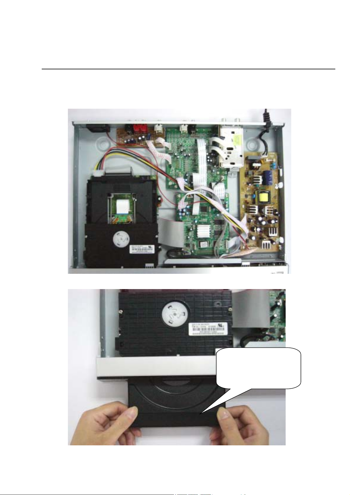
Step1: Remove the 8 screws around the top cover,
then remove top cover. (Figure 1)
2-1
Instructions
Step2: If it is necessary to dismantle Loader or Front Panel, It
should be remove the front door assembly first. (Figure 2)
Figure 1
Figure 2
Please kindly note that dismantle
the front door assembly carefully
to avoid damage tray and the
front door assembly.
2-2
g
Mechanical and Dismantling Instructions
Dismantling Instruction
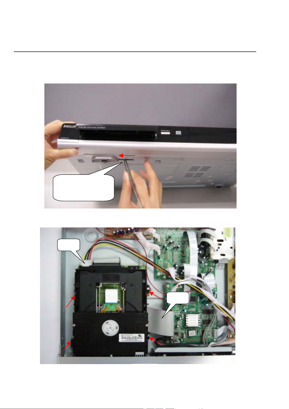
If the tray can’t open in normal way, you can make it
through the instruction as figure 3.
Note: Make sure to operate gently otherwise it would
be damaged
Push the guider until the
tray out. Make sure to
operate gently to avoid
e happening.
dama
CON 1
Step3: Dismantling Loader. First, disconnect the 2 connectors
then remove the 4 screws at both sides of the loader.
(Figure 4)
Figure 3
Figure 4
CON 2
2-3
Mechanical and Dismantling Instructions
Dismantling Instruction
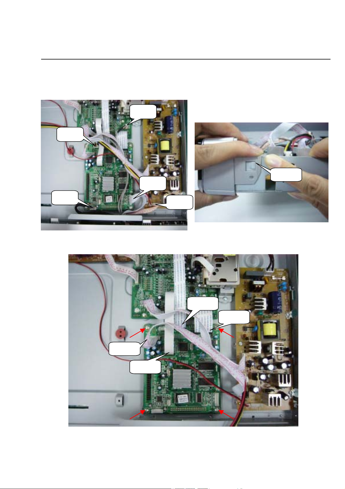
Step4: Dismantling the Front Panel: Disconnect the 5
connectors, and remove the 3 screws on the
bottom of the cabinet, then release the snaps on the
both sides of front panel, finally gently pull the panel
out from the set. (Figure 5&6 )
CON 5
CON 4
CON 6
CON 3
Figure 5
CON 9
CON 8
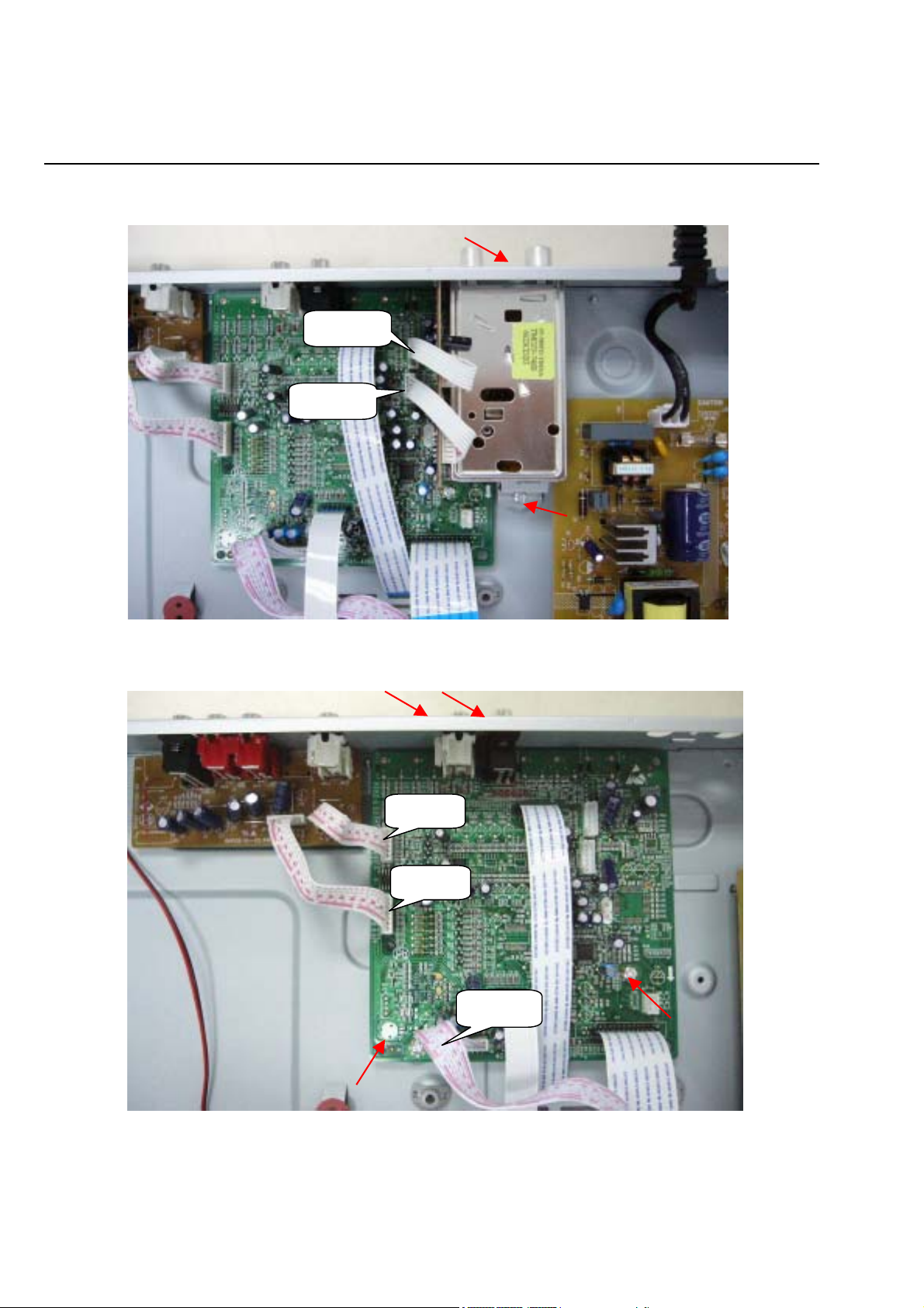
Step5: Dismantling Main Board, first disconnect the 4
connectors ,then remove 4 screws. (Figure 7)
CON 7
CON 10
Figure 7
Snap 1
Figure 6
CON 11
2-4
Mechanical and Dismantling Instructions
Dismantling Instruction
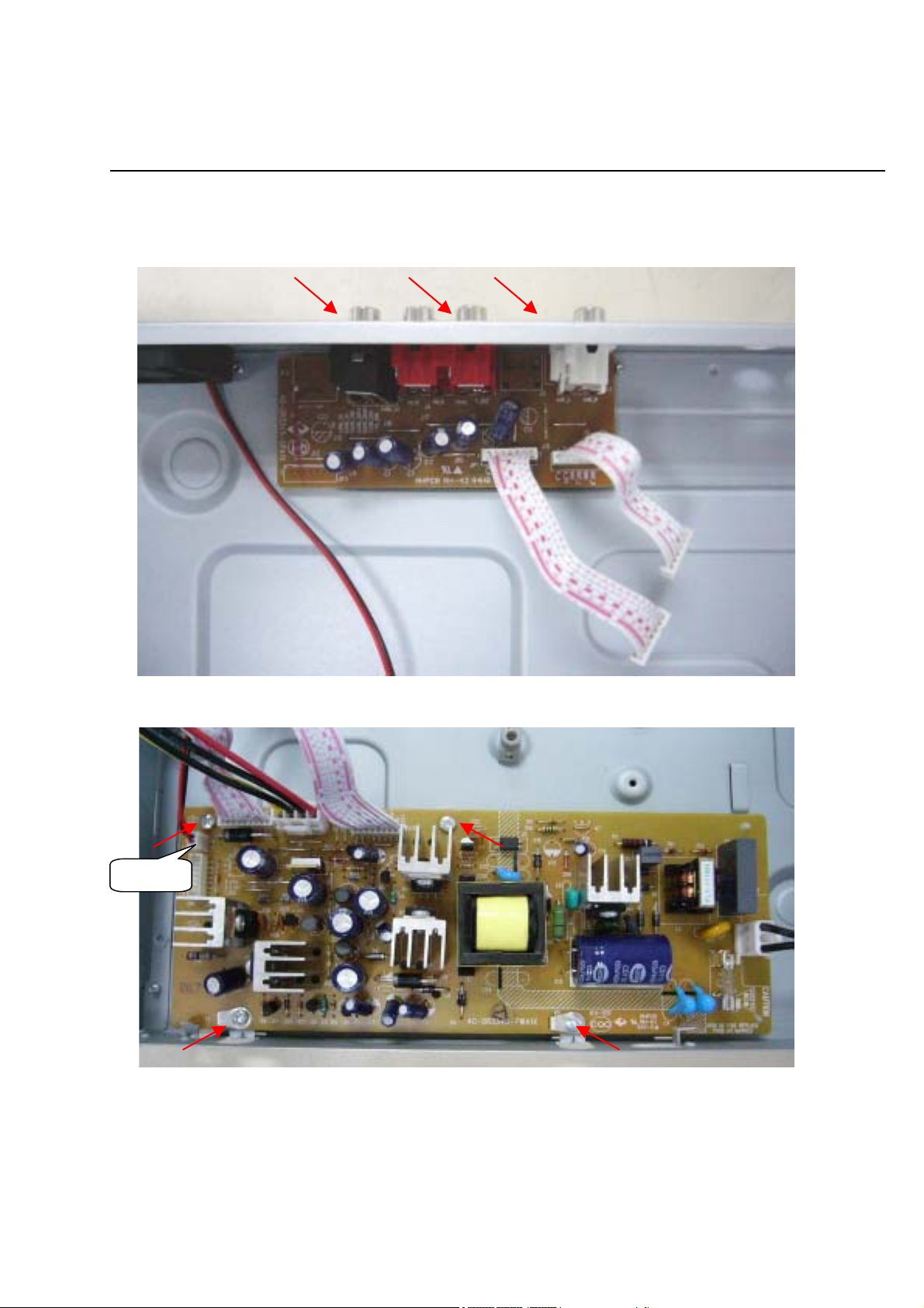
Step6: Dismantling Tuner Board: first disconnect the 2
connectors, then remove the 2 screws (Figure 8)
Step7: Dismantling AV Board, first disconnect the 3 connectors,
then remove
CON 13
CON 12
Figure 8
CON 16
CON 15
Figure 9
CON 14
the 4 screws. (Figure 9)
2-5
Mechanical and Dismantling Instructions
Dismantling Instruction
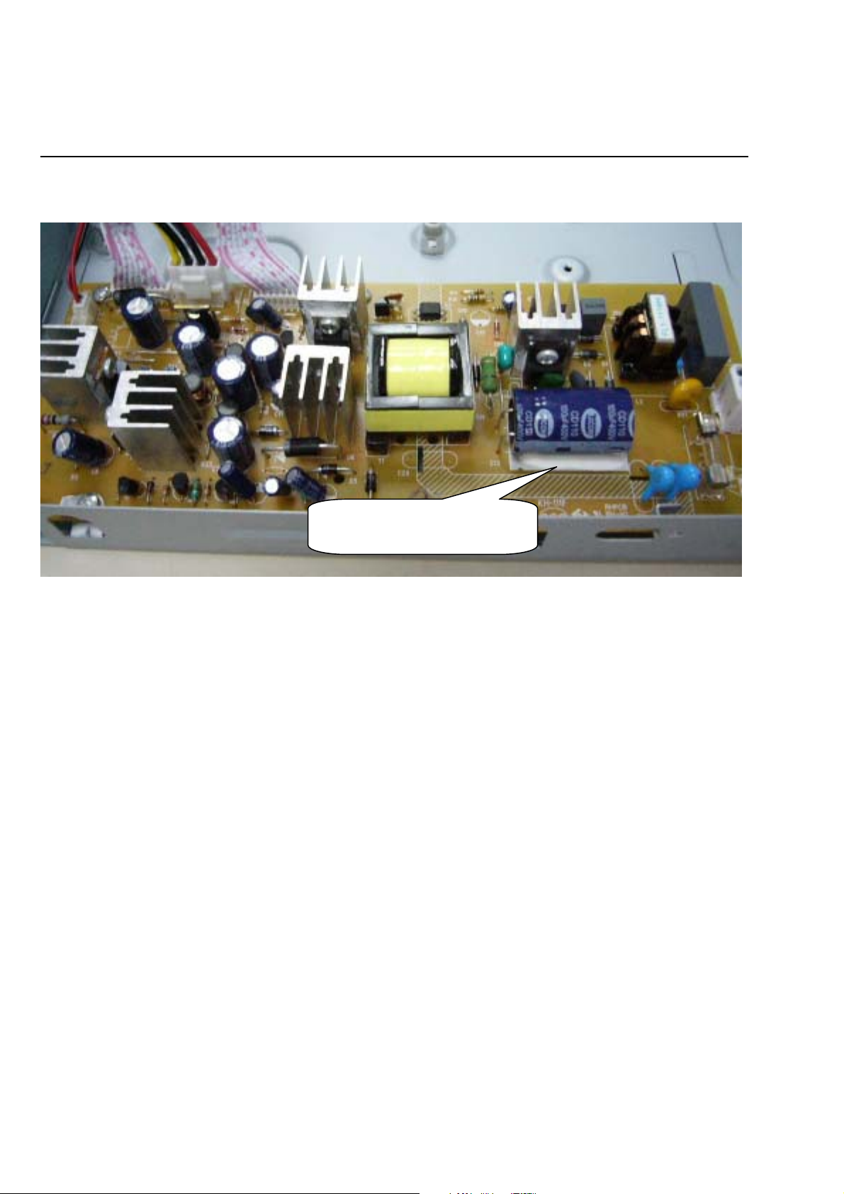
Step8: Remove the 3 screws on the back of
the cabinet, then dismantle the Output Board. (Figure
10)
CON 17
Step 9: Dismantling Power Board, first disconnect the 1
connector, then remove
Figure 10
Figure 11
the 4 screws. (Figure 11)
2-6
A
Mechanical and Dismantling Instructions
Dismantling Instruction
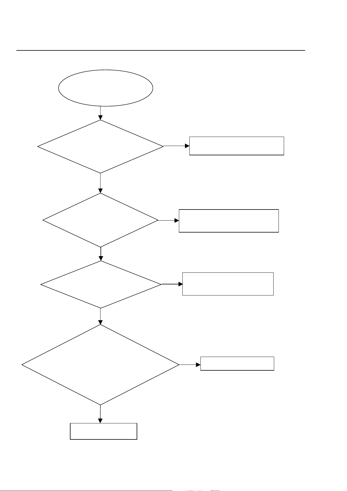
Step10: Make sure adding silicon glue to fix the capacitor after repairing. (Avoid the hazard of capacitor touching the top
cover Figure 12)
dd Silicon glue or Heat glue to
r Heat glue to fix
fix Capacitor keep this status
Capacitor keep this status
Figure 12

3-1
Region Code, Software Version& Upgrades
Software upgrade
A. Preparation to upgrade software
1) Start the CD Burning software and create a new CD
project (Data Disc) with the following setting:
Label: _____ (No need the label name)
File System: ISO9960
File Name: DVDR3408_93_V*.CUB
Remark: “
Note: It is required capital letter for the Label name
& the File System name.
2) Burn the data onto a blank CDR
B. Procedure for software upgrade:
1) Power up the set and insert the prepared Upgrade
CDR.
2) The set will start reading disc & response with the
following display on TV screen:
Software upgrade disc Detected, select OK to start
upgrading or CANCEL to exit.
Press OK button to start.
3) After press <OK> button to confirm, then screen will
display:
Upgrading software, please wait. Do not switch off
the power……
Please wait patiently, approximately two minutes
later the upgrading will complete.
4) The tray will automatically open when the upgrading
complete, and the TV will display:
System is successfully upgraded, Remove disc
from the tray and reset system.
5) According to the TV direction, take out the disc and
press OK, the tray will close, Reset the system.
” stand for the upgraded version number
*
C. Read out the software versions to confirm upgrading
1) Power up the set, Keep no disc in disc tray and the disc
door closed.
2) Press <0><0><0><9> <OK> button on remote control,
then the software version and other information will be
shown on the TV screen as follows:
Build: DVDR3408_93_VXX
Date: XXXX XX XXXX
Loader Version: XX.XX.XX.XX
Region Code: XXX
Caution: The set must not be power off during
upgrading, Otherwise the Main board will be
damaged entirely.
4-1
y
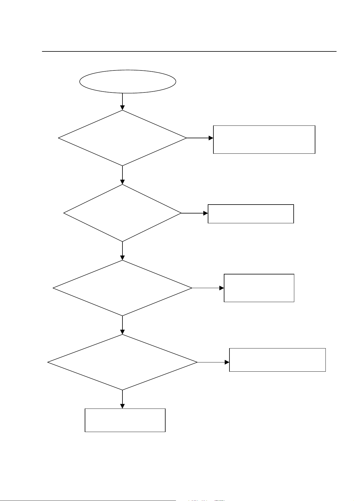
No display on VFD, and buttons do not work
Trouble shooting chart
No display on VFD, and
buttons do not work
Yes
Check every suppl
voltage on main board is
normal
No
Refer to Power supply board part
Yes
Check-24V+12V,VCC(+5v)
voltage on the power and front
board
No
Fix the connection JP1 on front board
and CN1 on power board
Yes
Check the front board
signals on R24, R25,
R28.(SCK,SDA,STB)
No
Check the U3’s pin 2,4,8 arrive the
U3’s pin 6,8,9 connect condition
Yes
1.Check whether bad solder
exists on U2 and pins of VFD,
2.Check whether the circuit
connected to K1, K2, K3, K4, K5
and K6 is broken.
No
Correct connection
Yes
Replace U2 or VFD
4-2
A
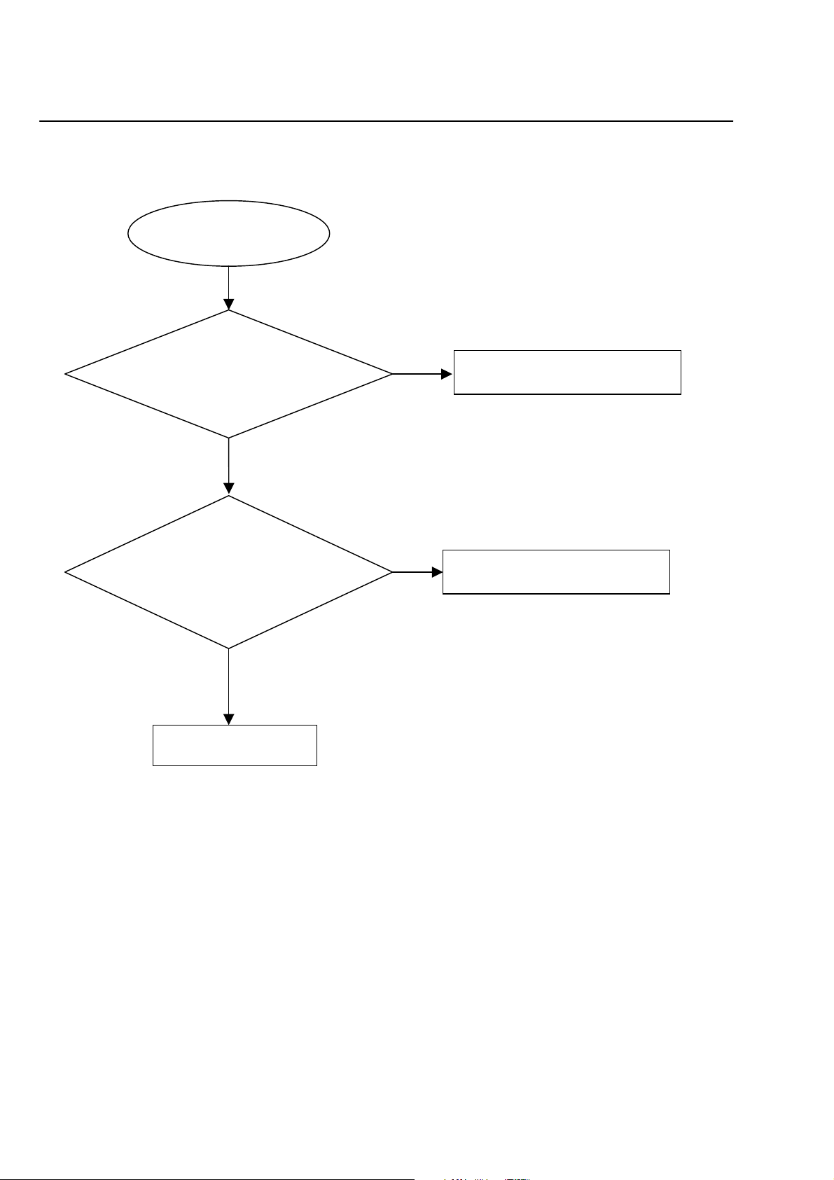
No digital audio output
Trouble shooting chart
No digital audio output
Go
Check the FB8 (digital audio) on
the Output board is normal.
Yes
No
Fix the connection JP8 on AV board
and JP2 on Output board
Yes
Check the R130
(digital audio) on the
V board is normal.
No
Check / Replace R131、C133.
Yes
Check the P14 of U10 on
the AV board is +5v
Yes
No
Check the +5v power
supply on the AV board
Yes
Check the P1 of U10 (digital
audio) on the AV board is
normal.
Yes
No
Check P26 of JP2 on Main board
signals is normal
Yes
Fix the connection JP8 on AV
board and JP2 on Main board
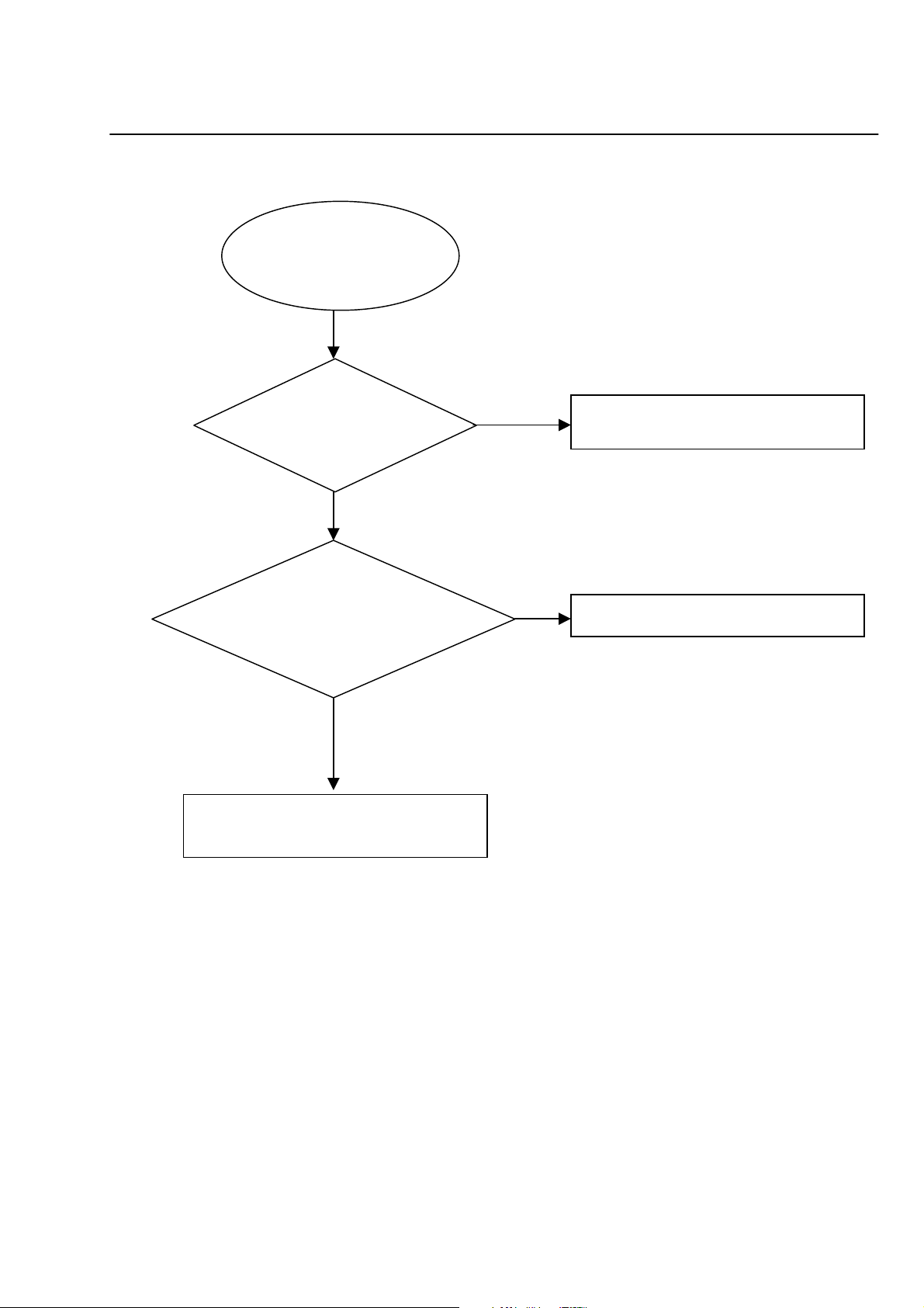
Remote control does not work
Remote control does
not work
Go
Check whether keys on the
front board work or not.
Yes
Check the front board
whether JP1 of U2 has
signal when pressing key
on the remote
Yes
Replace U1.
4-3
No
No
Yes
Replace U2 on the Front board
Replace U3 on the Front board
Trouble shooting chart
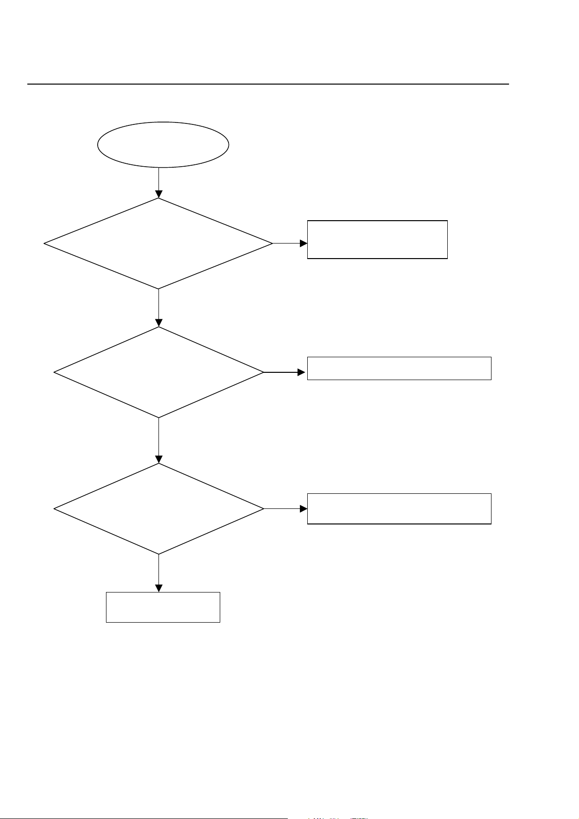
Can’t read disc or can’t open the tray
t
Can’t read disc or can’
open the tray
Go
Check whether the
DVD loader running is
normal
Yes
Check 40Pin cable from
main board connection to
the loader is normal
Yes
Check the peripheral components near the
J3 on the main board.
4-4
No
Trouble shooting chart
Check the connection of the 4Pin cable
from CN5 on the Power Board.
No
Fix the connection the 40Pin cable
4-5
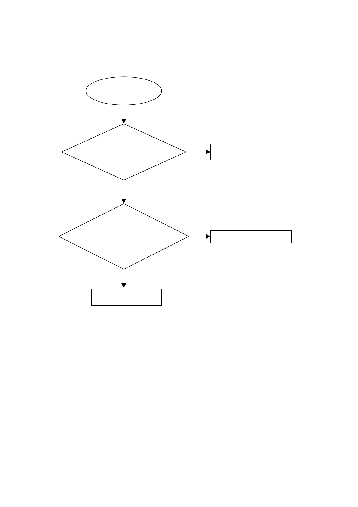
No VFD display
No VFD display
Go
Check whether the voltage
+12V/+5V on the front board
is normal work or not.
No
Fix the connection power board
CN1& front board JP1
Yes
Check whether the
voltage between VFD
F1&VFD F2 is AC3V
No
Check DC 12V to AC 3V switch circuit
Yes
Trouble shooting chart
Check whether the
voltage -24V is normal
No
Check the FB1 on the front board
Yes
Replace U2&VFD
4-6
r
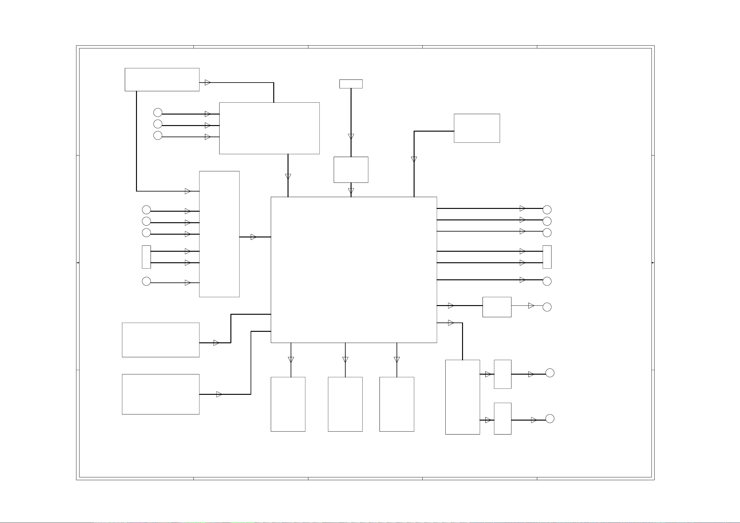
Fan don’t work
Fan don’t work
Go
Check on Power board
whether P1 of CN3 is
+12v
No
Check R9 on Power board
Yes
Check the cable
connection fan to Powe
board CN3
No
Replace the cable
Yes
Trouble shooting chart
Replace Fan
5-1
5-1
5
4
3
2
1
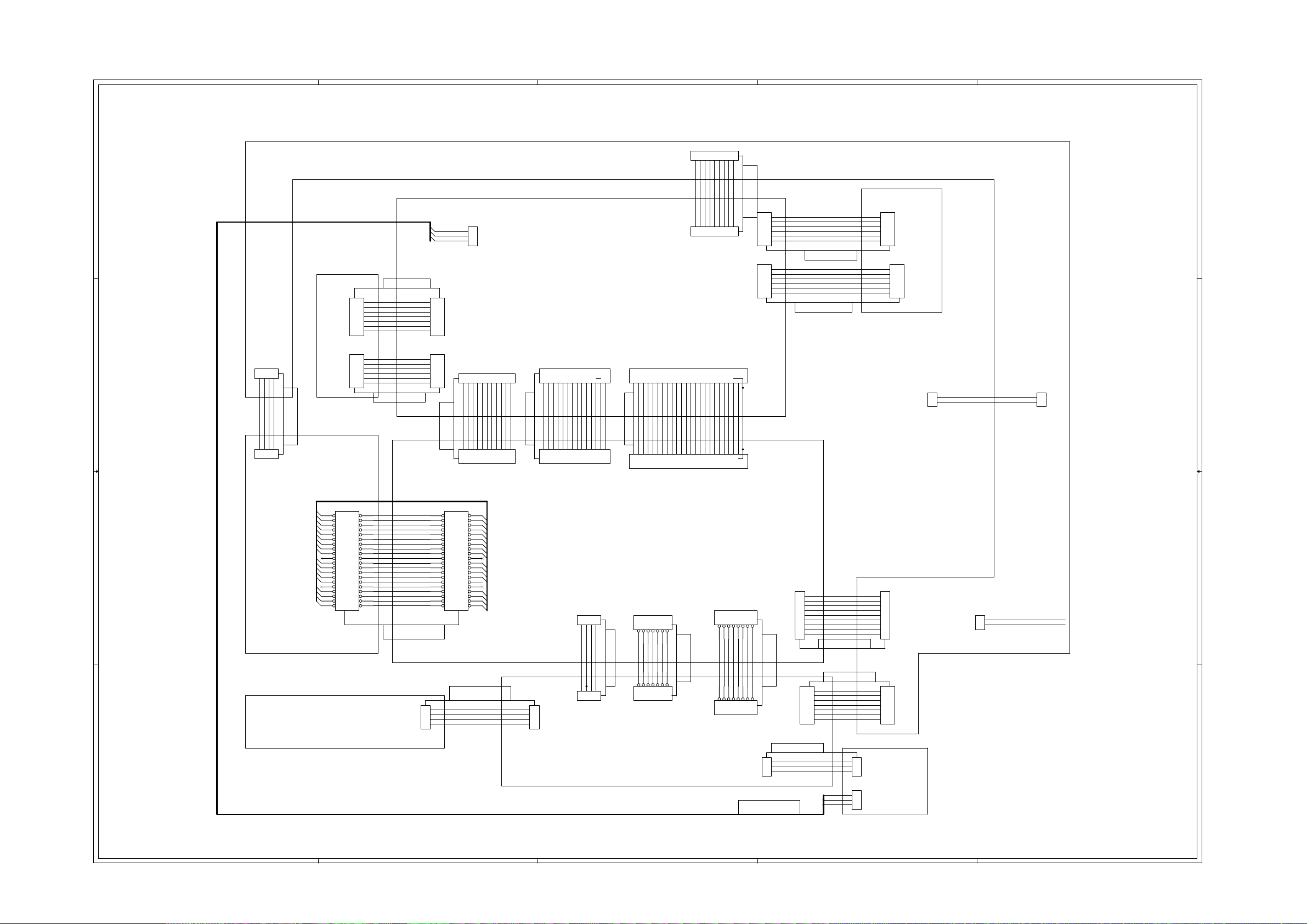
DVDR3408/93 BLOCK DIAGRAM
TUNER
D D
AUDIO IN 1
AUDIO IN 2
AUDIO IN 3
TUNER
C C
Y
Pb
VIDEO
DECODER
WM8776
AUDIO ADC
1EEE1394
POWER
1394
PHY
Y
Pb
Pr
Y
C
Pr
Y
C
DMN8602
CVBS
B B
LOADER ATAPI
BUFFER
WM8776
FORNT
PANEL KEY
IR & VFD
EEROM
FLASH
SDRAM
AUDIO
DAC
CVBS
S/PDIF
AUDIO LCH
A A
AUDIO RCH
BUFFER
5
4
3
2
1
5-2
A
Main Board
Power Board
5-2
A
B
C
D
E
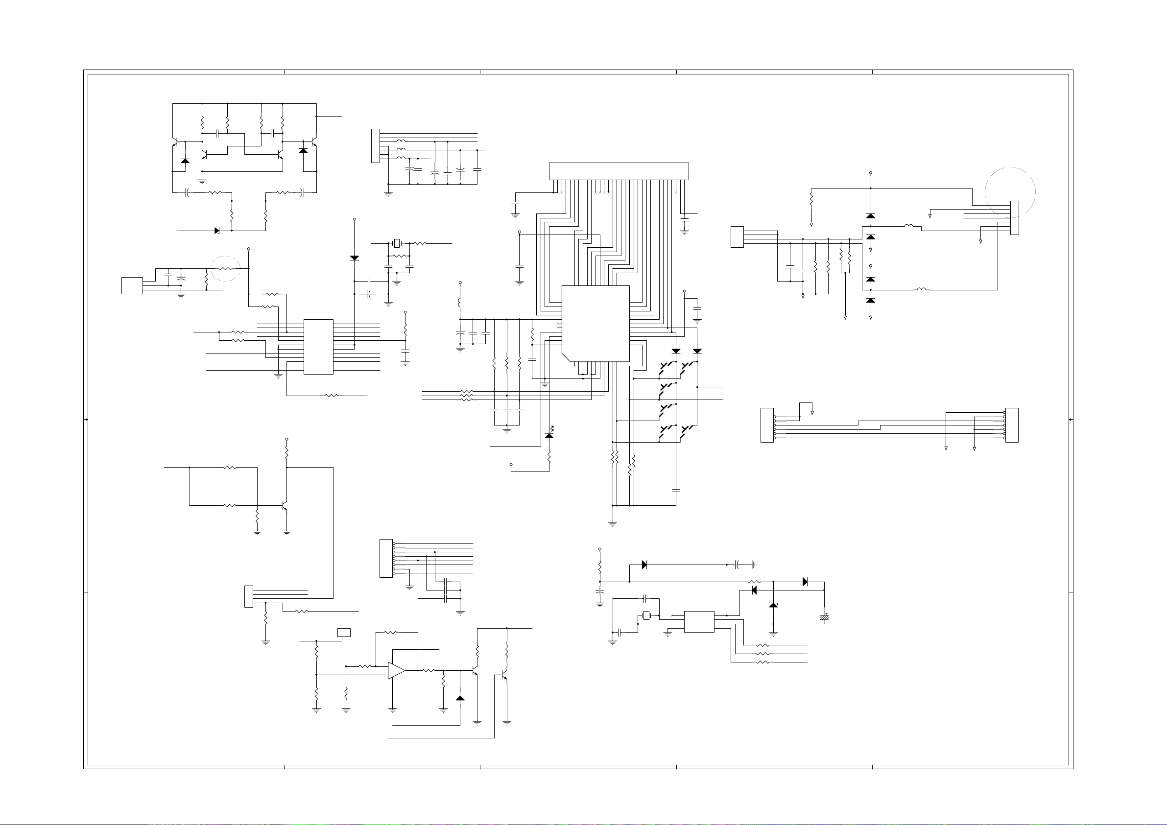
DVDR3408/93 WIRING DIAGRAM
CN4
123456789
CON9/2MM
4 4
GND
+12V
JP5
CON6/2MM
0818 L=250MM
6
5
4
3
2
1
JP6
CON6/2MM
6
5
4
3
2
1
24
+5VSTB
+5V
32V
GND
GND
GND
JP4
3
2
1
CON3/2MM
JP1
JP2
7
6
5
4
3
2
1
6
5
4
3
2
1
0815 L=80MM
CVBS
C
Y
GND
R
G
B
ROUT
GND
LOUT
VCC
GND
IEC_AUDIO
0814 L=80MM
CON7/2MM
7
6
5
4
3
2
1
JP7
CON6/2MM
6
5
4
3
2
1
JP8
JP10
FMN11/1.0mm
1234567891011
0811 L=140MM
123456789
JP5
FMN11/1.0mm
10
11
40-DR3345-AVB2G
JP9
FMN14/1.0mm
12345678910111213
0812 L=150MM
123456789
JP4
FMN14/1.0mm
Output Board
CON7/2MM
CN5
CON3/2MM
123
3 3
4
0810 L=380mm
+5V
GND
GND
+12V
123
4
CON6/2MM
40-DR3345-OPA1X
Loader
V Board
14
1011121314
JP3
0813 L=60mm
JP2
FMN24/1.0mm
JP1
123456789
CON9/2MM
1234567891011121314151617181920212223
123456789
101112131415161718192021222324
40-DR3345-PWA1X
Tuner Board
CON1
TV_SCL
TV_SDA
TV_V5
TV_V32
GND
VTUN_STB
0817 L=60MM
TV_AO
GND
TV_IF
TV_AFT
GND
TV_CVBSO
0816 L=60MM
CON6/2MM
6
5
4
3
2
1
CON2
CON6/2MM
6
5
4
3
2
1
40-TDK600-TUD1X
FAN
1
2
CN3
1
2
CON3
J19
1
2
3
4
PICH=2.0
J3
12
34
56
78
910
11 12
13 14
15 16
17 18
19 20
21 22
23 24
25 26
27 28
29 30
31 32
33 34
35 36
37 38
39 40
HEADER 20X2
0804 L=200MM
PW_SW1
PW_SW
LED1
GND
40-TDK600-MAB4G
J10
PICH=2.0
123
4
0806 L=320MM
123
J5
1
2
3
4
PICH=2.0
4
J2
PICH=2.0
40-DR3408-FVG2G
Front Board
J2
PH8/2MM
1234567
J3
PH8/2MM
1394
1394
0807 L=280MM
1234567
J4
PH8/2MM
8
GND
RS_G -12V
8
JP3
PH8/2MM
D_FM
IR
S_G
D_T
1234567
0808 L=150MM
R_M
A_M
1234567
0802 L=50MM
J2
7
6
5
0801 L=320MM
J1
CON9/2MM
1
2
3
4
5
6
7
8
9
JP1
PH7/2MM
0809 l=250
7
6
5
4
3
2
1
GND
GND
+3.3V
+3.3V
+5V
+2.5V
+2.5V
GND
GND
0803 L=120MM
P_C
VCC
GND
+12V
JP6
PICH/2MM
3
2
1
JP5
PICH/2MM
3
2
1
CN6
1
2
3
4
5
6
7
8
9
CON9/2MM
CN1
7
6
5
4
3
2
1
PH7/2MM
40-DR3408-INE2G
Input Board
CON2
J16
1
2
AC220V
AC220V
12
34
56
78
910
1112
1314
1516
1718
1920
2122
HEADER 20X2
2324
2526
2728
2930
3132
3334
3536
3738
3940
2 2
PHILIPS D5.1
0805 L=270MM
Switch Board
40-3408-SWA1G
1 1
A
B
C
D
E
6-1 6-1
5
4
3
2
1
DVDR3408/93 Front Board Electrical Diagram
+12V
Q2
8050DIP
D1
1N4148/D
+
C11
1N4148/SMT
U3
LH316S
1
P_CON
RDY
2
DATA
ATN
3
NC
OSC2
4
CS
OSC1
5
NC
RESET
6
VSS
VDD
7
VSS
VDD
8
CLK
SCK
9
SCL
D_FM
10
SDA
D_HOST
11
DATA_T
RST_TRST_M
R44
NC
+12V+12V
SDA
LED-2
R46
10K
R55
10K
IR
R27
NC
POWER_ LED
12 13
D7
24
23
22
21
20
19
18
17
16
15
14
CON1(RT)
2
VCC
FAN_CTL
1
R51
10K
R56
4.7K
JP1
PITCH=2.0
OSC_1
C22
100P
+
C23
47uF/16V
RDY_FM
ATN_FM
OSC_1
OSC_2
RESET
SCK_MPEG
D_FM
D_HOST
IR
RST_MPEG
To Power Board
1
FB1
2
3
FB2
4
5
FB3
6
7
47uF/16V
Y1
12MHz
R10
1M
C15
22P
JP3
1
2
3
4
5
6
7
8
PITCH=2.0MM
R45
1M
84
3
+
2
-
4558
P_CON
FAN_CTL
VCC
C6
+
100P
VCC
FB5
C25
+
47uF/16V
R24 100
R28 100
R25 100
RDY_FM
ATN_FM
SCK_MPEG
D_FM
D_HOST
IR
RST_MPEG
8050DIP
Q6
R54
3.3K
1N4148/SMT
D19
-24VV
32
F
34
35
36
37
38
39
40
41
42
43
44
LED-1
SACD
G4
G3
G2
G1
VDD
LED4
LED3
LED2
LED1
GND
OSC
VFD1 VFD-54
G6
G5
VEE
SEG11
SEG12
SEG13
SEG14
SEG15
SEG16
SEG6/K6
U2
SEG5/K5
PT6312
SEG4/K4
SEG3/K3
SEG2/K2
SEG1/K1
SW1
SW2
SW3
SW4
SDout
SDin
GND
SCLK
VCC
R33
10K
R34
10K
R41
1K
+
47UF/16V
/CS
C38
1234567891011
2324252627282930313233
SEG9
SEG10
SEG8
SEG7
KEY4
KEY3
KEY1
KEY2
C41
5P
VDD
R37
10K
22
21
20
19
18
17
16
15
14
13
12
R35
10K
D15 RB751
1 2
VCC
C40
5P
Y2
32.768K
P14
P13
P12
P11
P10P9P8P7P6P5P4P3P2P1NPNPNPNP1G2G3G4G5G6G7GNPF
D12
K1
K3
K4
K5
IDC Slave Addr: D0H/D1H
C8
100P
C7
10uF/50V
C27
C26
0.1u
0.1u
R20
10K
R47
50
8050DIP
Q7
C12
0.1u
-24VV
C17
0.1u
R21
R22
10K
10K
C30
C31
47P
47P
POWER_ LED
VCC
R48
100
+F2
R18
51K
C29
NC
C32
47P
FAN_CTL
R32
330
+12V
C5
C4
+
C3
VCC
+
100P
47uF/16V
R9
100
OSC_2
C16
22P
R16
10K
C28
0.1
CS
IDC_SCL
DATA POW_SW1
To Main Board
C36 100P
C37 NC
C39 NC
+12V
U5A
R53
1
10K
FFNP
P15
12318171615141312111098765419202122292827262524233031
+F1
C14
0.1u
VCC
C24
0.1u
1N4148/SMT
D13
K2
K6
C33
22P
U4
1
INT1
2
XIN
3
XOUT
4 5
GND RESET
HT1381
S_VIDEO_INPUT
1
2
3
4
S(VIDEO) OUT
JP2
1N4148/SMT
POW_SW
C35
47UF/16V
+
R42 470
D17 RB751
8
VCC1
7
SCL
6
SDA
R49 47
R50 47
R52 47
C18
33P
J4
6
5
4
3
2
1
1394 INTERFACE
12
D18
3.3V/0.5W
1 2
C21
33P
GND_VIN
D16 RB751
1 2
IDC_SCL
IDC_SDA
INT_FP
D3
LSV
GND_AV
R11
NC
GND_PHY_A
R12
NC
D8
LSV
E1
BATTERY3V
VCC
D9
GND_AV
LSV
VCC
GND_AV
GND_AV
1394 INPUT
Y_CIN
Y_CIN
1 2
1 2
1 2
1 2
D4
1N4148
1N4148
D10
1N4148
1N4148
BK1608HM601-T
D6
D11
FB4
GND_AIN
F_Y_IN
FB6
BK1608HM601-T
F_C_IN
GND_PHY_A
F_CVBS
GND_VIN
GND_PHY_A
MODIFY
C1 D5
C2 D5
C3 D4
C4 D4
C5 D4
C6 D4
C7 D4
C8 D4
C9 D5
C11 D4
C12 D3
C15 C4
C16 C4
C17 C3
C18 C2
C19 C5
C20 C5
C21 C2
C25 C3
C26 C3
C27 C3
C28 C4
C33 B2
C35 B2
C36 B4
C37 B4
C38 B3
C39 B4
C40 A3
C41 A3
D1 D4
D2 D5
D3 D2
D4 D1
D5 D5
D6 D1
D7 C4
D10 C2
D11 C2
D12 C2
D13 C2
D15 B3
D16 B1
D17 A2
D18 A2
FB1 D4
FB2 D4
FB3 D4
FB4 D1
FB5 C4
FB6 C1
J2
7
6
5
4
3
2
1
J3
1
2
3
4
5
6
7
PH7/2MM
2MM/PH7/TH
JP1 D4
JP2 D2
JP3 B4
J5 B5
R1 D5
R2 D5
R3 D5
R4 D5
R5 D5
R6 D4
R7 D5
R8 D5
R10 C4
R13 C5
R16 C4
R18 C3
R20 C3
R21 C3
R22 C3
R24 C4
R25 C4
R28 C4
R33 B3
R34 B3
R35 B3
R36 B5
R37 B3
R38 B5
R39 C5
R40 B5
R41 B3
R42 B2
R49 A2
R50 A2
R52 A2
Q1 D5
Q2 D4
Q3 D5
Q4 D5
Q5 B4
U1 C1
U2 C3
U3 C4
VFD D3
PITCH=2.0
8050DIP
R5
1
D5
5.6V/DIP
R2
3.3k
C1
104
Q3
R1
680/DIP
Q1
8050DIP
D D
1N4148/D
C9
10UF/50V
-24VV
D2
+
ADD
POW_SW
IDC_SDA
INT_FP
R13
4K7
IDC_SCL
R39
100
IR
R36
NC
R40
10K
10K(OPEN)
10K(OPEN)
U1
REM
3
VCC
2
GND
1
IR
C C
B B
+
C20
C19
47uF/16V
0.1u
P_CON
R3
R4
680/DIP
3.3k
C2
104
Q4
8050DIP
R6
+F2
+F1
R7
680
VCC
10K(OPEN)
R15
10K(OPEN)
P_CON
DATA
R17
CS
R19
R38
10K
1
10UF/50V
R8
680
R14
VCC
R31
820
Q5
2
3904
TO SWITCH BOARD
J5
1
2
3
4
PICH=2.0
A A
POW_SW
POW_SW1
R43
0
SDA
P_CON
5
4
3
2
1
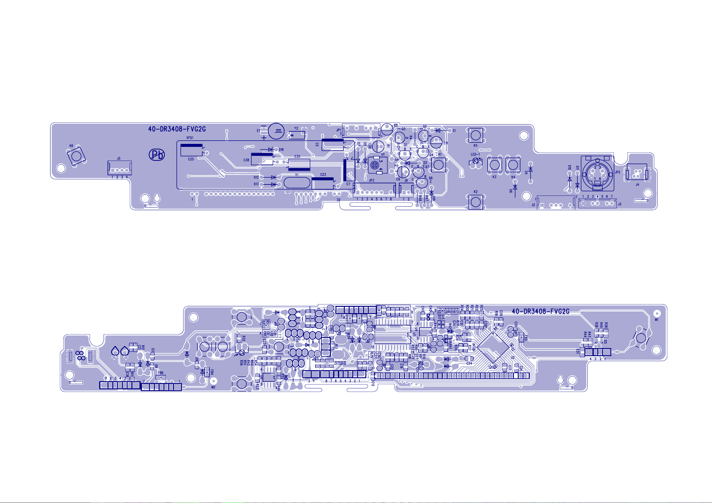
6-2
Front Board Print-layout (Top Side) for DVDR3408/93
6-2
Front Board Print-layout (Bottom Side) for DVDR3408/93
6-3
6-3
5
4
3
2
1
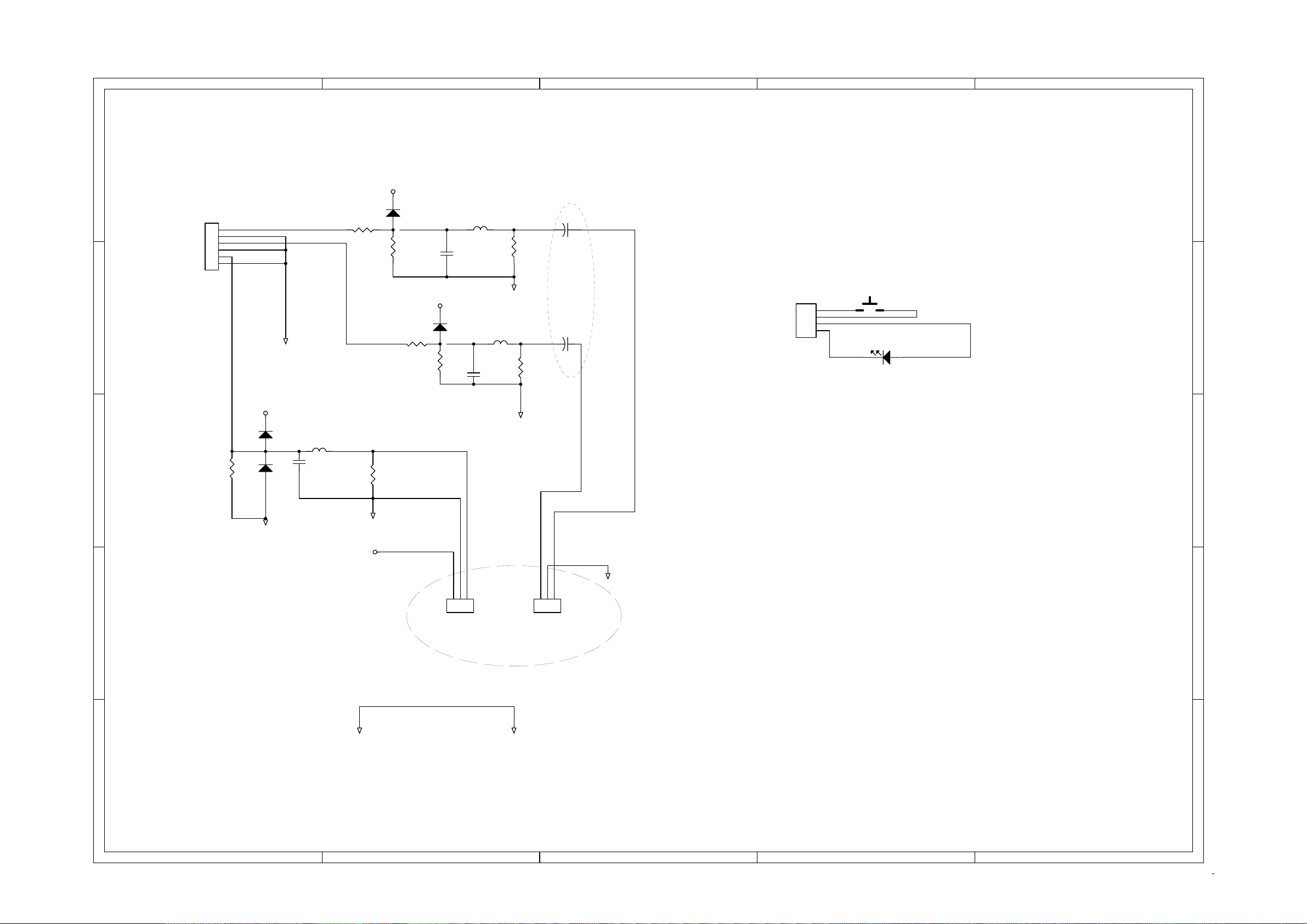
DVDR3408/93 Input Board & Switch Board Electrical Diagram
E E
VCC
D20
JP4
D D
C C
B B
AIN_RF
1
2
3
4
5
6
CVBS_IN
JP5(C_vbs L/R)
VCC
D25
LVS
GND_AV
GND_VIN
D24
1N4148
1 2
D26
1N4148
1 2
AIN_LF
FB9 BK1608HM601-T
C44
100P
R57
560
GND_VIN
VCC
1N4148
1 2
D21
LVS
VCC
D22
1N4148
R59
560
1 2
D23
LVS
VIDEO IN
F_CVBS
R61
75
JP6
PICH=2.0
AUDIO IN
FB7 BK1608HM601-T
R58
C42
100P
C43
100P
123
FB8 BK1608HM601-T
47K
GND_AIN
GND_AIN
10UF/16V
10UF/16V
R60
47K
AIN_LF
JP5
PICH=2.0
C46
+
C45
$''
SWITCH BOARD
+
J7
2MM
1
2
3
4
POWER_SWITCH
K7 POWER
POW_SW POW_SW1
POWER_LED
SACD
C42 D4
C43 C4
C44 C4
D24 C4
D26 C4
D25 C4
D20 D5
D21 D5
D24 C4
FB7 D4
AIN_RF
FB9 B4
JP4 D5
JP5 B4
JP6 B4
R57 D5
GND_AIN
R58 D4
R59 D5
123
0RGLILFDWLRQ
GND_AIN GND_VIN
A A
5
4
3
2
1
 Loading...