

Philips DVDR-3355, DVDR-3365 Service manual

DVD-Video Recorder
DVDR3355 & DVDR3365
DVDR3355/37/55 & DVDR3365/75/97
CLASS 1
LASER PRODUCT
Contents Page
1 Technical Specifi cations and Connection
Facilities 2
2 Safety Information, General Notes & Lead
Free Requirements 4
3 Directions for Use 6
4 Mechanical Instructions 8
5 Upgrade Software & Repair Chart 11
6 Block Diagrams,Waveforms, Wiring Diagram 19
Overall block diagram 19
Control block diagram 20
Wiring diagram 21
Waveforms of Analog Board 22
Waveforms of Digital Board 23
Test Point Overview for Analog Board 24
Test Point Overview for Digital Board 25
7 Circuit Diagram and PWB Layout 26
Analog: Frontend Video (FV) 26
Analog: Video In / Out (IOV) 27
Analog: Audio In / Out (IOA) 28
Analog: Power Supply (PS) 29
Analog: Multi Sound Processing (MSP) 30
Analog: Audio Converter (DAC_ADC) 31
Analog: Digital In / Out 1 (DIGIO 1) 32
Analog: Control Unit (CU) 33
Layout: Analog-Main Part (Top View) 34
Layout: Analog-Main Part (Bottom View) 35
Front: Front Panel - Display 40
Contents Page
Front: Front Panel - Audio/Video In 41
Layout: Front Panel (Top Copper Pattern) 42
Layout: Front Panel (Bottom Copper Pattern) 42
Front: Standby 43
Layout: Standby (Top View) 43
Layout: Standby (Bottom View) 43
Digital: Back-end Processor 44
Digital: Memory 45
Digital: IEEE 1394 Physical Layer 46
Digital: Video Input Processor 47
Digital: Interfaces 48
Layout: Digital-Main Part (Top View) 49
Layout: Digital-Main Part (Bottom View) 50
8 Circuit- and IC Description 51
Front Board 51
Analog Board 51
Digital Board 56
IC Description 59
Analog Board 59
Digital Board 64
9 Exploded View & Spare Parts List 75
Exploded View of the set 75
Spare Parts List 76
10 Revision List 81
©
Copyright 2005 Philips Consumer Electronics B.V. Eindhoven, The Netherlands.
All rights reserved. No part of this publication may be reproduced, stored in a
retrieval system or transmitted, in any form or by any means, electronic,
mechanical, photocopying, or otherwise without the prior permission of Philips.
Published by KC-TE 0519 AV Systems Printed in the Netherlands Subject to modifi cation EN 3139 785 30981
Version 1.1
EN 2
1.
3139 785 30981
Technical Specifi cations and Connection Facilities
1. Technical Specifi cations and Connection Facilities
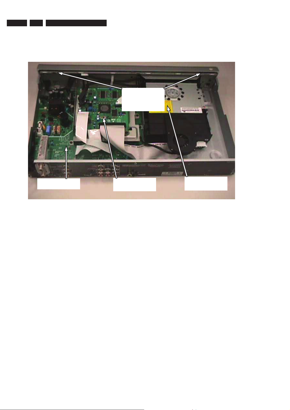
1.1 PCB Locations
Front boards
(Behind the
metal bracket)
Analog Board
Digital Board
1.2 General:
Power Supply : 127V /37
: 110V - 240V /55
: 220V - 240V /75/97
Consumption : 25 W (typical)
Standby power consumption : < 3 W
1.3 RF Tuner
Test equipment: Fluke 54200 TV Signal generator
Test streams: Philips Standard test pattern
1.3.1 System
NTSC-M
1.3.2 RF - Loop Through:
Frequency range : 45 - 860 MHz
Gain: (ANT IN - ANT OUT) : -6dB
Radio Interference / max. input
voltage, at 75, 3 tone method (
-40dB) : no limit
1.3.3 Modulator:
Video Modulation : 80%±15%
Frequency response : 0 ± 3dB, 0...4.2MH
Audio Modulation 1kHz tone : ± 12kHz, tol. ± 4kHz
Basic Engine
1.3.4 Receiver:
PLL tuning with AFC for optimum reception
Frequency range : 55 - 805 MHz
Sensitivity at 40 dB S/N : 60dBV at 75
(video unweighted)
1.3.5 Video Performance:
Channel 25 / 503,25 MHz,
Test pattern: standard test pattern.
RF Level 74dBV
Measured on Cinch Out
Frequency response : 0.1 - 3.58 MHz -1 ± 3dB
1.3.6 Audio Performance:
Audio Performance Analogue - HiFi:
Frequency response at Cinch (L+R)
output : 100 Hz - 10 kHz / 0 ±
3dB
S/N according to DIN 45405, 7, 1967
and PHILIPS standard test pattern
video signal : 45dB
Harmonic distortion (1 kHz, ± 25
kHz deviation) : 1.5%
1.3.7 Tuning
Automatic Search Tuning
Scanning time without antenna : typ. 3 min.
Stop level (vision carrier) : 37dBV
Maximum tuning error during
operation : ± 100 kHz
Manual Tuning
Manual selection in “STORE” mode

Technical Specifi cations and Connection Facilities
3139 785 30981
1.
EN 3
1.4 Analogue Inputs / Outputs
1.4.1 External In (Rear)
Video - Y/C (Hosiden)
according IEC 933-5
Superimposed DC-level on pin 4 (load 100k):
< 2.4V is detected as 4:3 aspect ratio
> 3.5V is detected as 16:9 aspect ratio
Input voltage Y : 1 Vpp ± 3dB
Input impedance Y : 75
Input voltage C : burst 300 mVpp ± 3dB
Input impedance C : 75
Video Cinch
Input voltage : 1 Vpp ± 3dB
Input impedance : 75
Audio Cinch
Input voltage : 2.2 Vrms max.
Input impedance : > 10k
1.4.2 Audio/Video Front Input Connectors
Audio
Input voltage : 2 Vrms max.
Input impedance : > 10k
Video - Cinch
Input voltage : 1 Vpp ± 3dB
Input impedance : 75
Video - YC (Hosiden)
according IEC 933-5
Superimposed DC-level on pin 4 (load 100 k):
< 2.4V is detected as 4:3 aspect ratio
> 3.5V is detected as 16:9 aspect ratio
Input voltage Y : 1 Vpp ± 3dB
Input impedance Y : 75
Input voltage C : burst 300 mVpp ± 3dB
Input impedance C : 75
1.4.3 Out 1
Component Video Cinch Y/Pb/Pr / Progressive Scan
according EIO-770-1-A, EIA-770-2-A
Audio - Cinch
Output voltage : 2 Vrms max
Output impedance : < 2k
1.4.4 Out 2
Video - Y/C (Hosiden)
Output voltage Y : 1 Vpp ± 3dB
C : burst 300 mVpp ± 1dB
Output impedance Y, C : 75
Video - Cinch
Output voltage : 1 Vpp ± 1dB
Output impedance : 75
Audio - Cinch
Output voltage : 2 Vrms max
Output impedance : < 1k
1.5 Video Performance DVD
All outputs loaded with 75 Ohm
SNR measurements over full bandwidth without weighting.
1.5.1 All Outputs
1.6 Audio Performance CD
1.6.1 Cinch Output Rear
Output voltage 2 channel mode : 2Vrms ± 1dB
Channel unbalance (1kHz) : <1dB
Crosstalk 1kHz : >100dB
Crosstalk 20Hz-20kHz : >87dB
Frequency response 20Hz-20kHz : ±0.2dB max
Signal to noise ratio (A-weighted) : >90dB
Dynamic range 1kHz : >83dB
Distortion and noise 1kHz : >83dB
Distortion and noise 20Hz-20kHz : >75dB
Intermodulation distortion : >70dB
Mute : >95dB
Outband attenuation: : >40dB above 30kHz
1.7 Digital Output
1.7.1 Coaxial
CDDA / LPCM : according IEC60958
MPEG1, MPEG2, AC3 audio : according IEC61937
DTS : according IEC61937
amendment 1
1.8 Digital Video Input (IEEE 1394)
1.8.1 Applicable Standards
Implementation according:
IEEE Std 1394-1995
IEC 61883 - Part 1
IEC 61883 - Part 2 SD-DVCR (02-01-1997)
Specifi cation of consumer use digital VCR’s using 6.3 mm
magnetic tape - dec. 1994
Mechanical connection according:
Annex A of 61883-1
1.9 Dimensions and Weight
Height of feet : 5.5mm
Apparatus tray closed : WxDxH:435x285x65mm
Apparatus tray open : WxDxH:435x422x65mm
Weight without packaging : app. 4 kg ± 0.5 kg
Weight in packaging : app. 6.0 kg
1.10 Laser Output Power & Wavelength
1.10.1 DVD
Output power during reading : 1.0mW
Output power during writing : 30mW
Wavelength : 650nm
1.10.2 CD
Output power : 1.0mW
Wavelength : 780nm
1.11 Write Speed
Type of Disc (Function) Disc Rotation Speed
Read Speed CD 7X CAV (25Hz)
Read Speed DVD 4X CAV (40Hz)
Write Speed DVD+RW 2.4X ZCAV
Write Speed DVD+R 2.4X ZCAV
SNR : > 48dB
Bandwidth : 4.2 MHz - 3dB
EN 4
2.
3139 785 30981
Safety Information, General Notes & Lead Free Requirements
2. Safety Information, General Notes & Lead Free Requirements
2.1 Safety Instructions
2.1.1 General Safety
Safety regulations require that during a repair:
• Connect the unit to the mains via an isolation transformer.
• Replace safety components, indicated by the symbol ,
only by components identical to the original ones. Any
other component substitution (other than original type)
may increase risk of fi re or electrical shock hazard.
Safety regulations require that after a repair, you must return
the unit in its original condition. Pay, in particular, attention to
the following points:
• Route the wires/cables correctly, and fi x them with the
mounted cable clamps.
• Check the insulation of the mains lead for external
damage.
• Check the electrical DC resistance between the mains
plug and the secondary side:
1. Unplug the mains cord, and connect a wire between
the two pins of the mains plug.
2. Set the mains switch to the ‘on’ position (keep the
mains cord unplugged!).
3. Measure the resistance value between the mains
plug and the front panel, controls, and chassis
bottom.
4. Repair or correct unit when the resistance
measurement is less than 1 M.
5. Verify this, before you return the unit to the customer/
user (ref. UL-standard no. 1492).
6. Switch the unit ‘off’, and remove the wire between the
two pins of the mains plug.
2.1.2 Laser Safety
This unit employs a laser. Only qualifi ed service personnel
may remove the cover, or attempt to service this device (due
to possible eye injury).
2.2 Warnings
2.2.1 General
• All ICs and many other semiconductors are susceptible to
electrostatic discharges (ESD, ). Careless handling
during repair can reduce life drastically. Make sure that,
during repair, you are at the same potential as the mass
of the set by a wristband with resistance. Keep
components and tools at this same potential.
Available ESD protection equipment:
– Complete kit ESD3 (small tablemat, wristband,
connection box, extension cable and earth cable)
4822 310 10671.
– Wristband tester 4822 344 13999.
• Be careful during measurements in the live voltage
section. The primary side of the power supply, including
the heatsink, carries live mains voltage when you
connect the player to the mains (even when the
player is ‘off’!). It is possible to touch copper tracks and/
or components in this unshielded primary area, when
you service the player. Service personnel must take
precautions to prevent touching this area or components
in this area. A ‘lightning stroke’ and a stripe-marked
printing on the printed wiring board, indicate the primary
side of the power supply.
• Never replace modules, or components, while the unit is
‘on’.
2.2.2 Laser
• The use of optical instruments with this product, will
increase eye hazard.
• Only qualifi ed service personnel may remove the cover or
attempt to service this device, due to possible eye injury.
• Repair handling should take place as much as possible
with a disc loaded inside the player.
• Text below is placed inside the unit, on the laser cover
shield:
Laser Device Unit
Type : Semiconductor laser
GaAlAs
Wavelength : 650 nm (DVD)
: 780 nm (VCD/CD)
Output Power : 20 mW
(DVD+RW writing)
: 0.8 mW
(DVD reading)
: 0.3 mW
(VCD/CD reading)
Beam divergence : 60 degree
CLASS 1
LASER PRODUCT
Figure 2-1
Note: Use of controls or adjustments or performance of
procedure other than those specifi ed herein, may result in
hazardous radiation exposure. Avoid direct exposure to beam.
CAUTION VISIBLE AND INVISIBLE LASER RADIATION WHEN OPEN AVOID EXPOSURE TO BEAM
ADVARSEL SYNLIG OG USYNLIG LASERSTRÅLING VED ÅBNING UNDGÅ UDSÆTTELSE FOR STRÅLING
ADVARSEL SYNLIG OG USYNLIG LASERSTRÅLING NÅR DEKSEL ÅPNES UNNGÅ EKSPONERING FOR STRÅLEN
VARNING SYNLIG OCH OSYNLIG LASERSTRÅLNING NÄR DENNA DEL ÄR ÖPPNAD BETRAKTA EJ STRÅLEN
VARO! AVATTAESSA OLET ALTTIINA NÄKYVÄLLE JA NÄKYMÄTTÖMÄLLE LASER SÄTEILYLLE. ÄLÄ KATSO SÄTEESEEN
VORSICHT SICHTBARE UND UNSICHTBARE LASERSTRAHLUNG WENN ABDECKUNG GEÖFFNET NICHT DEM STRAHL AUSSETSEN
DANGER VISIBLE AND INVISIBLE LASER RADIATION WHEN OPEN AVOID DIRECT EXPOSURE TO BEAM
ATTENTION RAYONNEMENT LASER VISIBLE ET INVISIBLE EN CAS D’OUVERTURE EXPOSITION DANGEREUSE AU FAISCEAU
Figure 2-2
2.2.3 Notes
Dolby
Manufactured under licence from Dolby Laboratories. “Dolby”,
“Pro Logic” and the double-D symbol are trademarks of Dolby
Laboratories. Confi dential Unpublished Works.
©1992-1997 Dolby Laboratories, Inc. All rights reserved.
Figure 2-3
Trusurround
TRUSURROUND, SRS and symbol (fi g 2-4) are trademarks
of SRS Labs, Inc. TRUSURROUND technology is
manufactured under licence frm SRS labs, Inc.
Figure 2-4
Safety Information, General Notes & Lead Free Requirements
3139 785 30981
2.
EN 5
Video Plus
“Video Plus+” and “PlusCode” are registered trademarks of
the Gemstar Development Corporation. The “Video Plus+”
system is manufactured under licence from the Gemstar
Development Corporation.
Figure 2-5
Macrovision
This product incorporates copyright protection technology that
is protected by method claims of certain U.S. patents and
other intellectual property rights owned by Macrovision
Corporation and other rights owners.
Use of this copyright protection technology must be
authorized by Macrovision Corporation, and is intended for
home and other limited viewing uses only unless otherwise
authorized by Macrovision Corporation. Reverse engineering
or disassembly is prohibited.
2.3 Lead Free Requirement
Information about Lead-free produced sets
Philips CE is starting production of lead-free sets from
1.1.2005 onwards.
INDENTIFICATION:
Regardless of special logo (not always indicated)
One must treat all sets from 1 Jan 2005 onwards, according
next rules.
Example S/N:
Due to lead-free technology some rules have to be respected by the
workshop during a repair:
• Use only lead-free solder alloy Philips SAC305 with order
code 0622 149 00106. If lead-free solder-pate is required,
please contact the manufacturer of your solder-equipment.
In general use of solder-paste within workshops should be
avoided because paste is not easy to store and to handle.
• Use only adequate solder tools applicable for lead-free
solder alloy. The solder tool must be able
o To reach at least a solder-temperature of 400°C,
o To stabilize the adjusted temperature at the solder-tip
o To exchange solder-tips for different applications.
• Adjust your solder tool so that a temperature around 360°C
– 380°C is reached and stabilized at the solder joint.
Heating-time of the solder-joint should not exceed ~ 4 sec.
Avoid temperatures above 400°C otherwise wear-out of tips
will rise drastically and fl ux-fl uid will be destroyed. To avoid
wear-out of tips switch off un-used equipment, or reduce
heat.
• Mix of lead-free solder alloy / parts with leaded solder alloy
/ parts is possible but PHILIPS recommends strongly to
avoid mixed solder alloy types (leaded and lead-free).
If one cannot avoid or does not know whether product is
lead-free, clean carefully the solder-joint from old solder
alloy and re-solder with new solder alloy (SAC305).
• Use only original spare-parts listed in the Service-Manuals.
Not listed standard-material (commodities) has to be
purchased at external companies.
• Special information for BGA-ICs:
- always use the 12nc-recognizable soldering temperature
profi le of the specifi c BGA (for de-soldering always use the
lead-free temperature profi le, in case of doubt)
- lead free BGA-ICs will be delivered in so-called ‘drypackaging’ (sealed pack including a silica gel pack) to
protect the IC against moisture. After opening, dependent
of MSL-level seen on indicator-label in the bag, the
BGA-IC possibly still has to be baked dry. (MSL=Moisture
Sensitivity Level). This will be communicated via AYSwebsite.
Do not re-use BGAs at all.
• For sets produced before 1.1.2005 (except products of
2004), containing leaded solder-alloy and components,
all needed spare-parts will be available till the end of the
service-period. For repair of such sets nothing changes.
Bottom line of typeplate gives a 14-digit S/N. Digit 5&6 is the year, digit 7&8 is
the week number, so in this case 1991 wk 18
So from 0501 onwards = from 1 Jan 2005 onwards
Important note: In fact also products of year 2004 must be treated in this way as long as you
avoid mixing solder-alloys (leaded/ lead-free). So best to always use SAC305 and the higher
temperatures belong to this.
• On our website www.atyourservice.ce.Philips.com you
BGA-de-/soldering (+ baking instructions)
Heating-profi les of BGAs and other ICs used in Philips-sets
You will fi nd this and more technical information within the
For additional questions please contact your local repair-helpdesk.
fi nd more information to:
“magazine”, chapter “workshop news”.

EN 6
3.
3139 785 30981
Directions For Use
3.
3. Directions For Use
The following except of the Quick Use Guide serves as an introduction to the set.
The Complete Direction for the Use can be downloaded in different languages from the internet site of Philips Customer care Center:
www.p4c.philips.com
QUICK USE GUIDE
1 what’s in the box
A
Main Unit
RF coaxial
C
cable
Video/Audio
D
(AV) cables
(yellow/red/white)
Remote control
B
includes 2x AA batteries
2 connect DVD recorder
Cable or
satellite signal
2a Connect existing antenna cable/satellite signal (or from
2b Use the supplied RF coaxial cable to connect the DVD
2c Use the supplied AV cables (yellow/red/white ends) to
2d Connect the power cable from the DVD recorder’s
Cable/satellite box jack panel
OUTIN
CH3 CH4
2a
2b
2d
the Cable/Satellite Box [RF OUT or TO TV]) to the
ANTENNA input jack at the back of the DVD
recorder.
recorder’s TV
jack.
connect the DVD recorder’s VIDEO (CVBS) and
AUDIO L/R OUT2 jacks to the matching Video/Audio
input jacks at the back of your TV.
~ MAINS to the AC power outlet.
Helpful Hint:
For additional types of connections, see User
Manual pages XX~XX.
output jack to your TV’s antenna input
DVD recorder back panel
2c
12nc: 3139 246 15331
3 Start initial setup
3a Insert batteries.
3b Press STANDBY-ON 2 on
the DVD recorder to turn it on.
Note: For successful installation,
your cable/satellite box must be
turned on.
3c Turn on the TV and select the
correct video in channel.
➜ The blue PHILIPS DVD
background screen will appear on the
TV.
3d Press SYSTEM MENU on the
remote control.
➜ Use 34 keys to go through the
menu. Select an item by pressing 2,
and confirm a setting by pressing OK.
System Menu - Channel Setup
Tuner Input Source
Channel Search
Modify Channel Information
System Menu - Channel Setup
Tuner Input Source
Channel Search
Modify Channel Information
System Menu - Language
On Screen Display Language
Default Disc Menu Language
Default Subtitle Language
Default Audio Language
System Menu - Clock
Date (mm/dd/yy)
Time (hh:mm:ss}
Show DivX® Registration Code
The DVD recorder is ready for use!
See next page for basic recording and playback.
3e Highlight and press 2.
Cable
Search
Edit
Cable
Search
Edit
Setup and install TV channels.
1 Select { Tuner Input Source. }
–{ Cable } if the DVD recorder is
–{ Air } if the DVD recorder is
2Select { Channel Search } and
3f Highlight and press 2.
English
English
English
English
Select the language.
– select TV On-Screen Display
– select default Disc Menu language.
– select default subtitle language.
– select default audio language.
3g Highlight and press 2.
01/31/05
10:33:57AM
OK
Set the Date and Time.
Use the numeric keypad 0-9 to
input the date/time, then press OK
to confirm.
3h Press SYSTEM MENU to exit.
DVDR3355
connected via a cable/satellite box.
connected directly to the antenna
wall outlet.
press OK on the remote control
to start automatic TV channel
search.
language.

3.
ALL
1
Directions For Use
3139 785 30981
3.
EN 7
4 start manual recording
4a Insert a recordable DVD+R/
+RW with the label facing up.
4b To record TV program, press
REC SOURCE to select
{ Tuner. }
To record from an additional
device connected to this DVD
Recorder, press REC SOURCE
repeatedly to select the
corresponding external input
channel : { Front CVBS, }
{ Front S-Video, } { Rear CVBS, }
{ Rear S-Video, } { DV. }
4c Press REC MODE to select a
desired recording mode.
It defines the picture quality and
the maximum recording
time for a disc.
Record
Mode
1 Hour Mode
2 Hour Mode
4 Hour Mode
6 Hour Mode
Picture Quality
High quality
DVD quality-Standard Play
VHS quality-Extended Play
VHS quality-Super Long Play
Maximum Recording
Time per Disc
1 hour
2 hours
4 hours
6 hours
5 start playback
To playback a disc
5a Insert a disc with the label side
facing up.
5b Playback may start automatically.
If not, press
➜ If a disc menu appears,
use 1234 keys to navigate
within the menu, highlight a title and
press OK to start playback.
5c To stop playback, press
STOP9.
To watch the TV
programs
5d Press REC SOURCE to select
{ Tuner, } then use 34 keys to
select the program number.
SUPER VIDEO
PLAY 2.
4d Press REC 0 to start recording.
GET PICTURE
• Check the AV mode on TV. It may be called FRONT, A/V IN, or
4e To pause the recording,
press ;. To resume recording,
press REC 0.
To stop the recording, press
STOP 9.
➜ Wait until the message
disappears from the display panel
before you remove the disc.
NEED HELP? Read the accompanying User Manual or visit our website www.philips.com/support
VIDEO. Choose the different modes using TV remote control.
• Or, use the TV remote control to select Channel 1 on TV, then
press Channel down button until you get the picture.
• Or, select CHANNEL 3 or 4 on the TV if you are using a
RF modulator or Cable/Satellite Box.
• See your TV manual for more details.
GET SOUND
• Connect the AUDIO L/R (red/white) jacks at the back of the DVD
recorder to the correspond AUDIO input jacks on a TV, stereo
system or receiver. Turn on the connected system and select the
appropriate channel.

EN 8
4
3139 785 30981
4. Mechanical Instructions
Mechanical Instructions
4.1 Dismantling and Assembly of the Set
For item numbers please see the exploded view in Chapter 9.
4.1.1 Dismantling of the DVD Loader Tray Cover
1) Inserting a minus screw driver and push the lever in the
direction as shown in Figure 4-1 to unlock the tray before
sliding it out.
Figure 4-1
2) Remove the Tray Cover as shown in Figure 4-2.
4.1.2 Dismantling of the Front Panel Assembly
1) Remove the 3 screws 188 and release the 2 snap hooks
on the side before removing the front assembly.
1
Figure 4-3
2) Remove the 5 screws 186 to remove the front plate 184
as shown in Figure 4-4.
Figure 4-2
2
2
Figure 4-4
Mechanical Instructions
3139 785 30981
4
EN 9
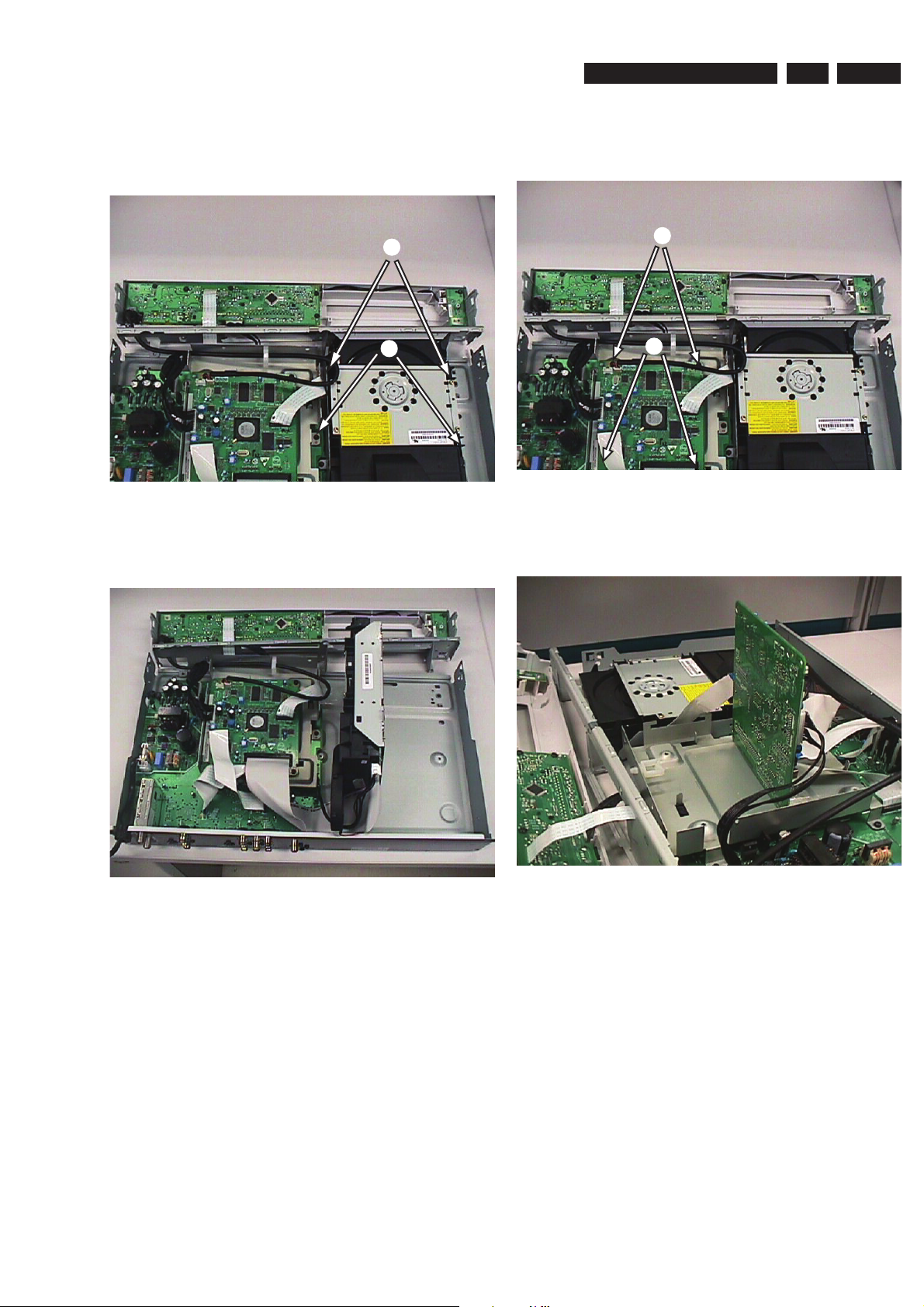
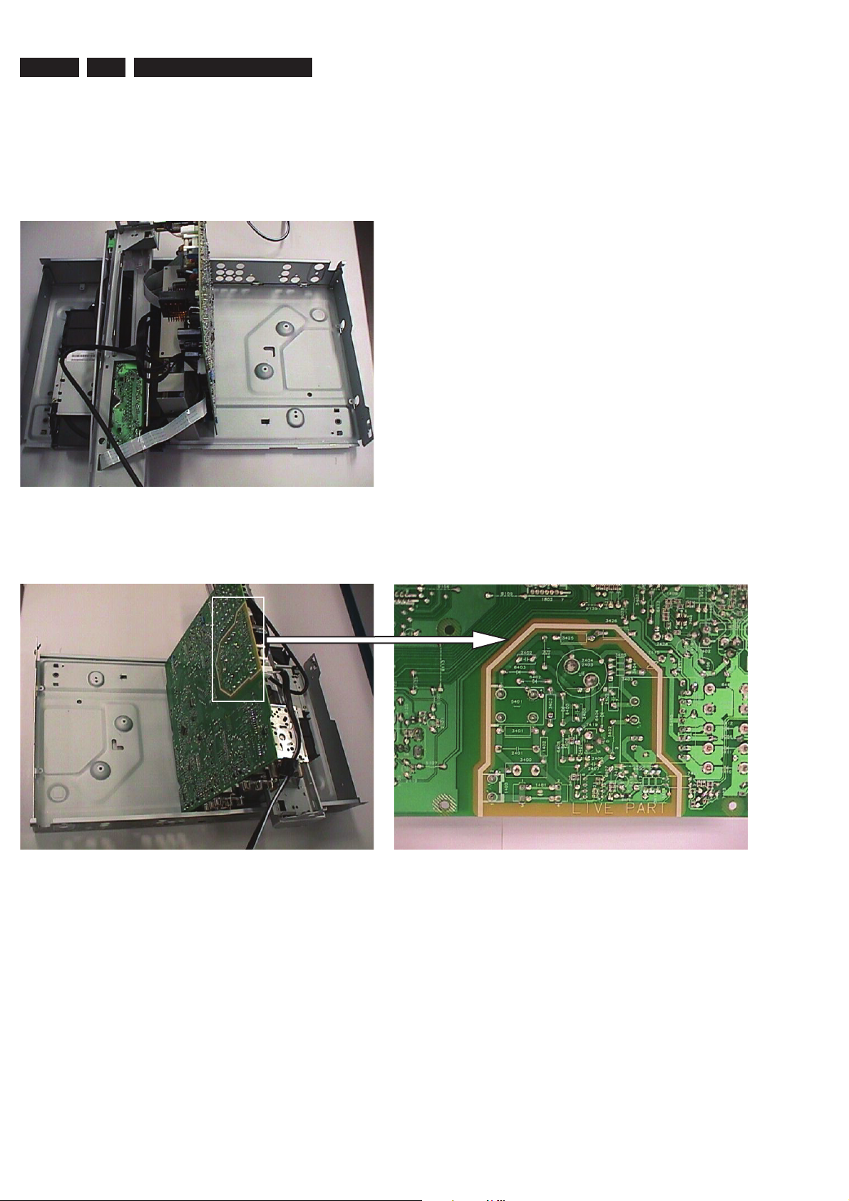
4.1.3 Dismantling of the Basic Engine
1) Remove the Cover Tray (See 4.1.1).
2) Remove the 4 screws 260 to free the Basic Engine.
3
3
Figure 4-5
3) Place the Basic Engine in the service position by fl ipping
the basic engine to the vertical position
4.1.4 Dismantling of the Digital Board
1) Remove the 4 screws 272 to loose the Digital Board as
shown in Figure 4-7.
4
4
Figure 4-7
2) Service Position can be achieved by fl ipping the Digital
board to the Vertical Position as shown in Figure 4-8.
Figure 4-6
Figure 4-8
Note: The cable (just to transfer the service connection to the
analog board) from socket 1101 can be removed and use for
hyperterminal connection.
EN 10
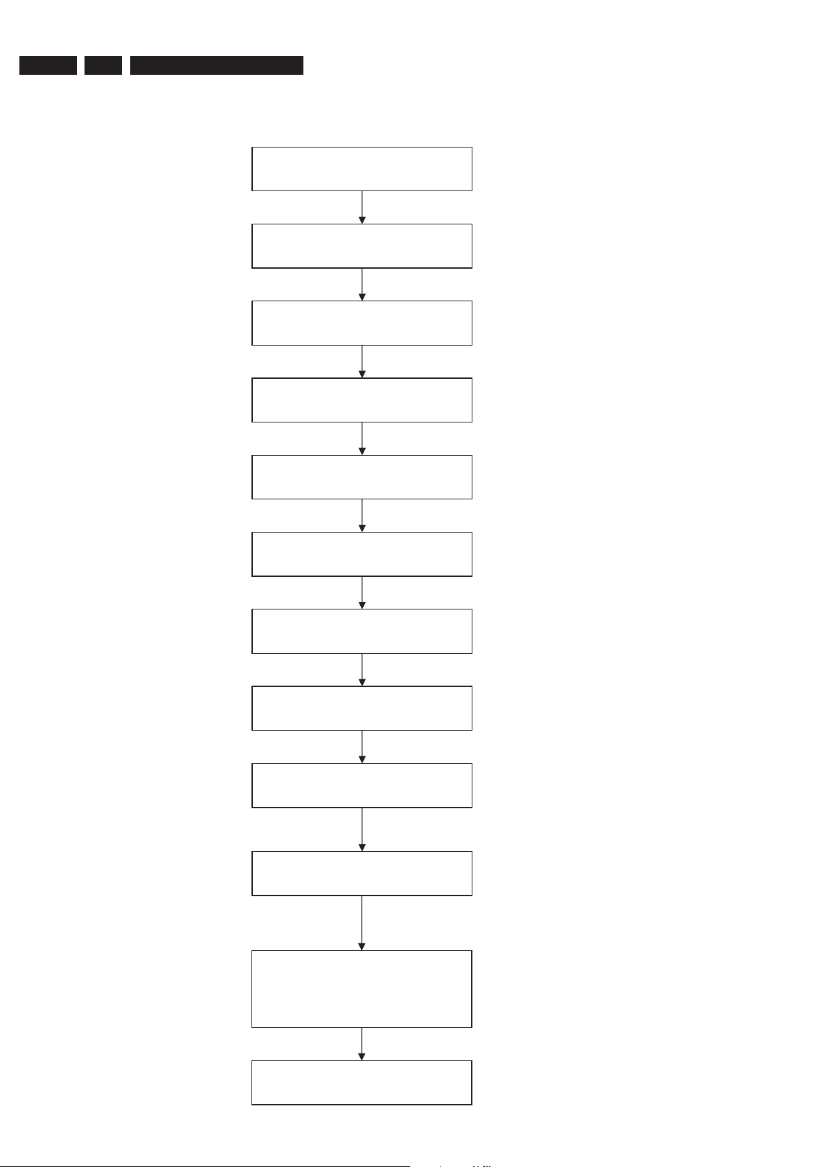
4.1.5 Dismantling of the Analog Board
4
1) Remove 5 screws 244 and 4 screws 252 and screw 230.
2) Remove 4 screws 270 and 3 screws 268.
3) Service Position can be achieved by fl ipping the analog
board to the Vertical Position as shown in Figure 4-9.
3139 785 30981
Mechanical Instructions
Figure 4-9
Note: Please cover the Live Area during trouble-shooting.
(Figure 4-10)
Figure 4-10
Figure Live Area

Upgrade Software & Repair Chart
3139 785 30981
5. Upgrade Software & Repair Chart
5.1 A. Preparation to upgrade fi rmware:
1. Unzip the zip-archive fi le
2. Start the CD Burning software and create a new CD project (data disc) with the following settings:
File system: Joliet
Format: MODE 2: CDROM XA
Recording mode: SINGLE SESSION (TRACK-AT-ONCE), FINALIZED CD
Note: Long fi le name is necessary for the preparation of the upgrade disc
3. Place the content of the zip-archive into the root directory of the new CD project.
4. Burn the data onto a blank CDR or CD-RW
B. Procedure to apply the fi rmware upgrade:
1. Power up the set and open tray.
2. Insert the prepared Upgrade CDROM and close the tray,
3. The TV connected to the set will display:
Software Upgrade Disc detected
Select OK to start or CANCEL to exit
4. Press OK button to confi rm upgrading (use left/right button for selection)
5. The TV connected to the set will display:
5.
EN 11
Upgrading Software, Please wait
Do not switch off the power
6. When the upgrading process is successful the tray will open and the TV connected to the set will display:
System is successfully upgraded.
Remove disc from tray & reset system
7. Remove the Upgrade Disc and press OK button to confi rm
8. The TV screen goes blank, tray close and after a while the Philips Logo screen appear again.
C. How to read out the fi rmware version to confi rm upgrading
1. Power up the set and with no disc in the tray
2. Press <0009> and <OK> buttons on the remote control
EN 12
5.
3139 785 30981
5.2 Repair Chart
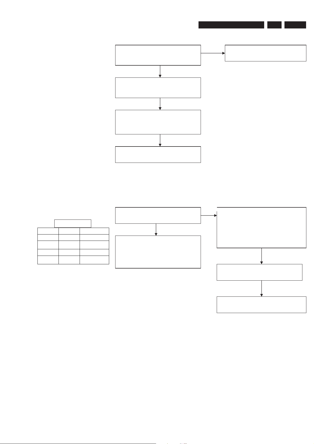
5.2.1 Completely Dead Set
Upgrade Software & Repair Chart
Check primary fuse Holder 1401
OK
Check Voltage at Fuse
1405,1406,1407,1408,1409,1410
OK
Check Voltage at
F424,F434,F406,F439,F409,F447,F449,F457
OK
Check STBY at F441=high?
OK
Measure Voltage across F420 & F459
OK
Check DRAIN (pin 8) at F417 = 300V?
OK
Check waveform at
F417, I407, I409
OK
Check front board for Supply
F115=4.85V- 4.95V
OK
Check Clock
F132 & F131 =32K768MHz
OK
Check Power_Fail
At F126 = 5V?
OK
Check digital board
T516 = 1.8V
T515 = 2.5V
T201 = 1.25V
T202 = 1.25V
OK
Check connectivity at inductor 5291 or
voltage at capacitor 2291 = 3V3
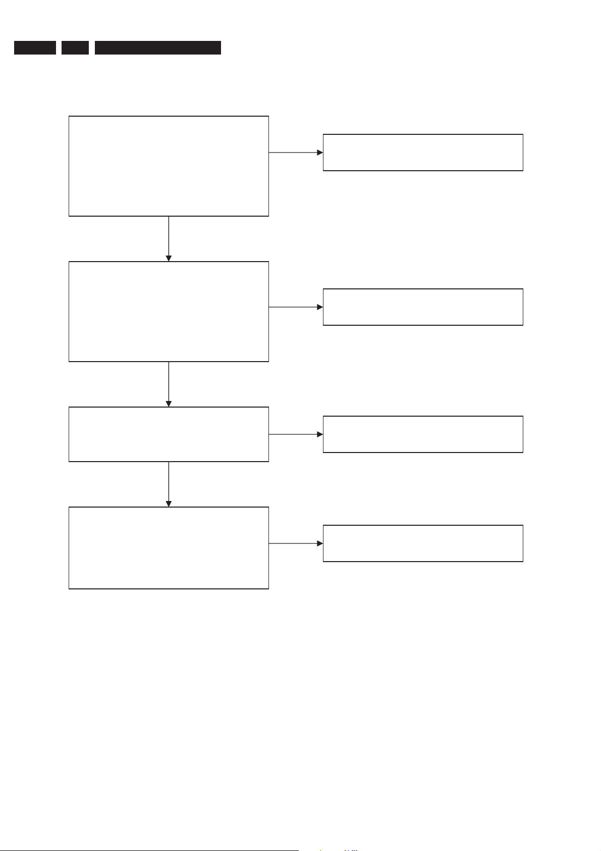
5.2.2 Cannot Read Disk
416
Upgrade Software & Repair Chart
3139 785 30981
5.
EN 13
Check cable connection:
Supply cable from Analog 1404 to Drive
1600 (4 pin)
Check cable connection:
Analog 1571 to Drive 1600 (40 pin)
Check Voltage at analog board
F415 = 12V
F
=5V
Check Fuse I406
Replace Loader
OK
OK
OK
OK
5.2.3 Disk Unknown
Check Cable connection
Supply cable 1404 on Analog to 1600 (4 pin)
on loader
OK
Checks whether correct region code?
OK
Replace Loader
EN 14
5.
3139 785 30981
5.2.4 Audio No Sound (Playback)
Upgrade Software & Repair Chart
Check Test Point
I603, I604, I605, I609 = square pulse
OK
Check Test Point
I613 = 11.2V –12V
I624 = 3.3V
I615 = high
OK
Monitor Test Point
I618 & I620 = 1KHz 2Vrms Sine Wave
OK
Monitor Test Point
I616 & I617 = 3.3V
OK
Monitor Test Point
I600 = -5V (high)
OK
Monitor Test Point
F603 = <0.6V (low)
OK
Monitor Test Point
I601 = 5V (high)
OK
Monitor Test Point
F451 = 5V (high)
OK
Monitor Test Point
I419 = >0.6V (high)
Upgrade Software & Repair Chart
3139 785 30981
5.
EN 15
5.2.5 Audio No Sound (TV & External Source)
Part 1
Check I316 & I319 = sine wave
&
Check I606 & I607= sine wave
OK
Check Test Point
SYSCLK I608 = square pulse 12.28MHz
F609, F610, F611 = square Pulse
OK
Check control line
I612 = 0V (low)
I611 = 1.7 V
I610 = 1.6V
OK
Check supply voltage
I614
No
Replace the component in between these 2
test point (Op Amp 7300)
Part 2
Truth Table
Pin 9 Pin 10 Source
0 0 Tuner
0 1 Rear In 1
1 0 FRONT AV-in
1 1 Rear In 2
(reserved)
(CVBS, YC)
Check I310 & I311
Verify against Truth Table
OK
IF MDX pin 3 & 13 = no sine wave
Verify Input of MDX 7301
I312, I313, I314, I315
No
Check MSP (7500) Xtal at I509 = 18.432MHz
Check Supply voltage at
I513 = 8V
I508 = 5V
I515 = 5V
Check I2C At
I500 & I501
OK
I503 = 4.5MHz 300~500mVpp Sine wave
OK
Touch up joint
OR
Replace IC MSP (7500)
EN 16
5.
3139 785 30981
Upgrade Software & Repair Chart
5.2.6 No Video Out Upon Power ON (Assume set is not dead)
Check Digital Board Waveform at
CVBS T524
Y T522
C T523
CY T520
BPb T518
BPr T521
OK
Check Cable Connection on Analog Board
Check Test point for Waveform
CVBS F235
C F236
Y F237
D-VR F238
D_YG F239
D_UB F240
OK
Check Test point for Waveform
CVBS F221
C F218
OK
Replace Digital Board If no Waveform
NO
Replace transistors if no waveform
NO
Replace transistors if no waveform
OK
Check Test point for Waveform
CVBS F222
C F220
Y F219
D_VR F215
D_YG F213
D_UB F214
NO
Replace transistors if no waveform

5.2.7 No Video In Only
Check Supply on digital board
Upgrade Software & Repair Chart
OK
3139 785 30981
5.
EN 17
Check Clock At
T432 & T461 = 14.318MHz
Check Video Input
T524, T526, T527, T528, T529, T530, T531,
T532 T533 T535
Replace VIP (7401) IC
5.2.8 Tuner Not Functioning
Check Voltage
OK
OK
I119 = 33V
F101 = 5V
OK
NO
NO
NO
Replace Crystal 1461
Check respective i/p test point
of video in at analog board
Replace Digital Board
Check I100 & I102 On I2C
OK
Direct access tuner to any channel.
If there are video and no audio. Check MSP Xtal
OK
F104 for AFT signal = DC level
Scan direct –changing of tuner
18V-36V
NO
NO
Replace Tuner
Alignment Out.
Replace Tuner

EN 18
Notes:
5.
3139 785 30981
Upgrade Software & Repair Chart
EN 19
3139 785 30981
6.
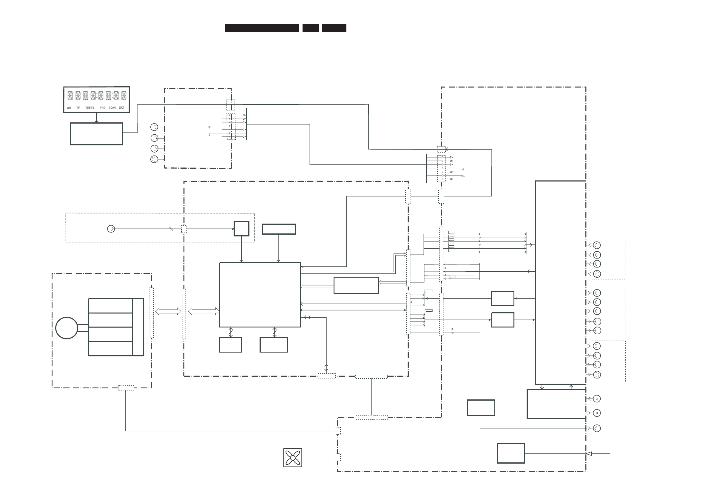
6. Block Diagrams, Waveforms, Wiring Diagram
Block Diagrams, Waveforms, Wiring Diagram.
Overall Block Diagram of the Set
Front Keyboards
Digital Video
Input IEEE1394
CVBS-YUV-Y/C
AUDIO PCM I2S
A_BCLK
A_WCLK
A_DATA
SPDIF_OUT
D_KILL
AUDIO ENCODER I2S
YUV-YC-CVBS
ANALOG AUDIO / VIDEO
D_CVBS
D_C
D_Y
D_V
D_Y1
D_U
A_V
A_U
A_Y
A_C
TUNER
INPUT/OUTPUT
PROCESSING &
SOURCE
SELECTION
ANALOG BOARD
MAINS
AC
F439
F440
F441
F442
F443
F444
2
1
AFCRI
AFCLI
CVBSFIN
CFIN
YFIN
3
4
5
7
9
1922
1201
1512
1204
1205
1600
1536
S-VIDEO
CVBS
AUDIO R
AUDIO L
AINFR
AINFL
CVBSFIN
CFIN
YFIN
ADC
7
9
11
12
13
14
15
12
14
16
18
20
22
DDRAM
FLASH
VIDEO INPUT
PROCESSING
DIGITAL AUDIO
RS232
SERVICE
1111
1522
1551
DIG.VIDEO
21
20
18
2
16
7
1
3
5
7
9
S-VIDEO
CVBS
RF IN - ANTENNA
RF OUT - TV
PHY
F438
DIGITAL AUDIO OUT
DOMINO DMN-8602
MPEG 2, AC3 CODEC
EEPROM
DIGITAL AUDIO
I2C
A_PCMCLK
A_xCLK
BUFFER
A_YCVBS
DAC
D_DATA0
D_WCLK
D_BCLK
9
11
12
14
D_PCMCLK
D_xCLK
ANALOG VIDEO
1800
POWER
SUPPLY
PSU
5N
GND5VGND
GND
12V
GND
3V3
3V3
3V3
3V3
1403
1
12
-5V
GND
ION
+5V
GND
GND
+12V
GND
+3V3
+3V3
+3V3
+3V3
1501
1
12
CONTROL LINES
CONTR
OL LINES SCK,D_FM,D_HOST,RDY_FM,ATN_FM,HOST_RESET
IDE BUS
FAN
1804
6
IDE BUS
1934
IN-EXT2
OUT2
OUT1
DIGITAL BOARD - DIMENSION
DVD+RW ENGINE D4.3
TRAY CONTROL
SERVO
READ
WRITE
DISC
PSU
40
LASER
1600-1
+5V
GND
GND
+12V
1600-2
1571
AUDIO L/R
Y
Pb
Pr
AUDIO L/R
S-VIDEO
CVBS
AUDIO L/R
CONTROL LINES, AND SUPPLY LINES
1803
(LOOP THROUGH)
CONTROL UNIT SLAVE
MICROPROCESSOR
VPD 16316GB-006
For Digital Video version only
(OPTION)
(OPTION)
EN 20
3139 785 30981
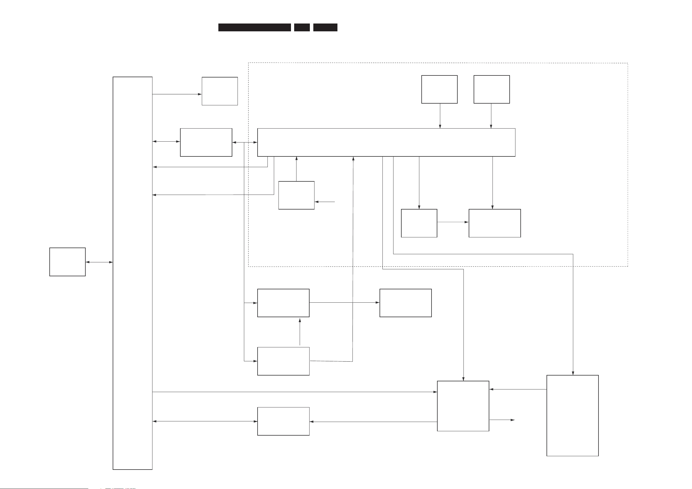
6.Block Diagrams, Waveforms, Wiring Diagram.
Control Block Diagram Analog Board
Frontend
Tune r
I2C Bu s
Repeater
ASP Analog Sl av e Processo r
NEC uPD-16316GBT
A udio Switches
HEF4052 B
Fa n
>=1
Rese t
Multi Sound
Processo r
MSP34x 5
ADC / DA C
>=1
KILL
Supply
VF T
Displa y
Po we r
Supply
RC
Fr ont
Ke ys
DIGIT AL BO ARD DIMENSION
DV D R
I2 C
D_KILL_ N
IDE0
HOST_Reset
I2 C
5V
IN T
I2 C
3V 3
Reset
5VSTBY
AF C
2
2
2
1
1
35
STBY
IP FA I L
AKILL
MUTE
RSA1,RSA2
FRONT Boar d
FAN_CTRL
Control Block Diagram
EN 21
3139 785 30981
6.
Block Diagrams, Waveforms, Wiring Diagram.
Wiring Diagram
Interconnection Diagram Architecture DVDR3355 V1.0 Kek YH
06.01.2005
FRONT PCB
MAINS AIO COM VIO KB_FC FAN KB_FC
CORD 1600 1800 1205 1206 1803 1804 1201
1 MAINS P 1
GND
20 GND 1 A_YG
1
GND 1 FAN_P
14
GND
2 MAINS L 2
DAOUT
19 SCL0 2 GNDV
2
SCK 2 FAN_N
13
SCK
3
GND
18 SDA0 3 A_UB
3
D_FM
12
D_FM
4
DAINOPT
17
RDY_FM
4 GNDV
4
D_HOST
11
D_HOST
5
NO_CONNECT
16
D_FM
5A_VR
5
GND
10
GND
6
DAINCOAX
15
D_HOST
6 GNDV
6
RDY_FM
9
RDY_FM
7
MUTE
14 GND
24
7 Y_FIN
7
ATN_FM
8
ATN_FM
PDUDIG
8
GND
13
SCK 23
8 GNDV
8
HOST_RESET
7
HOST_RESET
1403
9
D_PCMCLK
12 ATN_FM
22
9 C_FIN
9
RC_IN
IPFAI
L
6
RC_IN
10
GND
11 HOST_RESET
21
10 CVBS_FIN
10
5VSTBY
1204
5
5VSTBY
1 3V3 11
D_DATA0
10
CVBS_Y SW 20
11 GNDV
11
STBY(POWER_CTRL)
1
YFIN
4
STBY(POWER_C
2 3V3 12
D_WLCK
9
AIN_SEL0 19
12 C_REAR
12
IPFAIL
2
GND
3
IPFAIL
3 3V3 13
GND
8
AIN_SEL1 18
13 GNDV
13
VGNSTBY
3
CFIN
2
VGNSTBY
412VEF 14
D_BLCK
7
TU_DET 17
14 Y_REAR
14
12VSTBY
4
GND
1
12VSTBY
5 GND 15
GND
6
FAN CTRL 16
15 GNDV
5
CVBS_FIN
612
V
16
A
_PCMCL
K
5
FBIN 15
16 CVBS_REA
R
PSUDRIVE
6
GND
FA
V
7 GND 17
GND
4
SC 2 pin 8_1 14
17 GNDV
1404
7
AL_FIN
1300
8 GND 18
A_DATA
3
SC 2 pin 8_2 13
18 CVBS_TU
8
GND
1
YFIN
95V 19
GND
2
RC 12
19 GNDV 1 12VE
9
AINFR
2
GND
10 5V 20
A_WCLK
1 GND
11
20 D_CVBS 2 GND
3
CFIN
11 GND 21
A_BCLK 10
21 GNDV 3 GND
4
GND
12 5N 22
GND 9
22 D_C 45VE
5
CVBS_FIN
823
GNDV
ANALOG DVDR_3355
6
GND
724
D_Y
7
AL_FIN
625
GNDV
8
GND
526
D_VR
9
AR_FIN
427
GNDV
328
D_YG
2 29 GNDV
1 30 D_UB
Front Drive
DV-In PSUDRIVE
JST LC
112VE
2 GND
3 GND
45VE
USB
1401/1402
15VUSB1
2 USB1_D+
PSDIG AIO COM VIO IDE_ IDE_ 3 USB1_D-
1501 1536 1551 1522 1521 1571 4 GND
1 3V3 22 GND 1 GND 30 VIA_GY
1 RESETn
1 RESETn
2 3V3 21 BCKI 2 SCL0 29 GNDV
2
GND 2 GND
STDBY KEY
3 3V3 20 WCKI 3 SDA0 28 VIA_BPb
3
DD[7] 3 DD[7]
0100
4 3V3 19 GND 4 RDY_FM 27 GNDV
4
DD[8] 4 DD[8] 1 KEY1
5 GND 18 DAI (0) 5 D_FM 26 VIA_RPr
5
DD[6] 5 DD[6] 2 KEY2
6 12V 17 GND 6 D_HOST 25 GNDV
6
DD[9] 6 DD[9]
7 GND 16 MCKI 7 GND
24
24 VIA_SY_FR
7
DD[5] 7 DD[5]
8 GND 15 GND 8 FPSCK
23
23 GNDV
8
DD[10] 8 DD[10]
9 5V 14 BCKO 9 ATN_FM
22
22 VIA_SC_FR 9 DD[4] 9 DD[4]
10 5V 13 GND 10 HOST_RESET 21 21 VIA_CVBS_FR PH2mm 10 DD[11] 10 DD[11]
11 GND 12 WCKO 11 VIOSW 20 20 GNDV 1512 11 DD[3] 11 DD[3]
12 NC 11 DAO (0) 12 AIN_SEL0 19 19 VIA_SC_RE 12 DD[12] 12 DD[12]
10 GND 13 AIN_SEL1 18 18 GNDV 1 TPBn 13 DD[2] 13 DD[2]
9 MCKO 14 COM_ARST 17 17 VIA_SY_RE 2 TPB 14 DD[13] 14 DD[13]
8 GND 15 FAN CTRL 16 16 GNDV 3 GND 15 DD[1] 15 DD[1]
7 MUTE 16 FBIN 15 15 VIA_CVBS_RE 4 TPAn 16 DD[14] 16 DD[14]
6 NC 17 SBS0 14 14 GNDV 5 TPA 17 DD[0] 17 DD[0]
5 NC 18 SBS 1 13 13 VIA_CVBS_TU 6 GND 18 DD[15] 18 DD[15]
4 NC 19 FPIR 12 12 GNDV 19 GND 19 GND
3 GND 20 GND 11 11 VOA_CVBS 20 Keypin 20 Keypin
2 SPO 10 10 GNDV 21 DMARQ 21 DMARQ
1 GND 9 9 VOA_SC 22 GND 22 GND
8 8 GNDV 23 DIOW_n 23 DIOW_n
7 7 VOA_SY 24 GND 24 GND
6 6 GNDV 25 DIOR_n 25 DIOR_n
5 5 VOA_RPr 26 GND 26 GND
4 4 GNDV 27 IORDY 27 IORDY STDBY KEY
3
3
VOA_GY
USB 28 CSEL
28 CSEL
1302
2 2 GNDV 1502 29 DMACK_n 29 DMACK_n 1 KEY1
DIGITAL BOARD 1 1 VOA_BPb 1 5VUSB1 30 GND 30 GND 2 KEY2
2 USB1_D+ 31 INTRQ 31 INTRQ
3 USB1_D- 32 IOCS16 32 IOCS16
4 GND 33 DA1 33 DA1
34 PDIAG_n 34 PDIAG_n
35 DA0 35 DA0
36 DA2 36 DA2
37 CS0_n 37 CS0_n
38 CS1_n 38 CS1_n
39 DASP_n 39 DASP_n
40 GND 40 GND
8002
140mm
8003
140mm
8008
tbc mm
8001
120mm
8010
280mm
8007
180m
8012
140mm
8013
tbc mm
to be confirmed if
8011 and 8012
needs to be
to be confirmed if
8008 and 8013
needs to be
combined
8014
220mm
EN 22
3139 785 30981
6.Block Diagrams, Waveforms, Wiring Diagram.
Waveforms
Waveforms of Analog Board
F219 Y_OUT F220 C_OUT F222 CVBS_OUT F236 C_OUT F237 Y_OUT F238 D_VR
F239 D_YG F240 D_UB F417 VDrain (No Disc) F417 Vdrain(Standby) I300 & I301 AIN2R & AIN2L I302 & I304 AFER & AFEL
I316 & I319 IC7301 PIN 13 & 3
I407 Vgate (No Disc) I407 Vgate (Standby) I409 VSource (No Disc) I409 VSource (Standby) I621 & I619 ARDAC & ALADC
I702 DAOUT M_ARDAC
EN 23
3139 785 30981
6.
Block Diagrams, Waveforms, Wiring Diagram.
Waveforms of Digital Board
IC 7211 PIN 45 IC 7211 PIN 46 IC 7401 PIN74 IC 7401 PIN75 T121
T122 T351 IC7301 PIN 42 T352 IC 7301 PIN 43
T525, T526,T529
CVBS_TU, CVBS_RE,CVBS_FR
T527,T531,T535 SY_RE,SY_FR, CY
T528,T530 SC_RE, SC_FR T532 BPr T533 BPb T537 BCK T538 WCK
T539 DA T540 MCK
EN 24
3139 785 30981
6.Block Diagrams, Waveforms, Wiring Diagram.
Test Points Overview for Analog Board
AnalogBd_TestPoint_31916.pdf 2005-09-07
EN 25
3139 785 30981
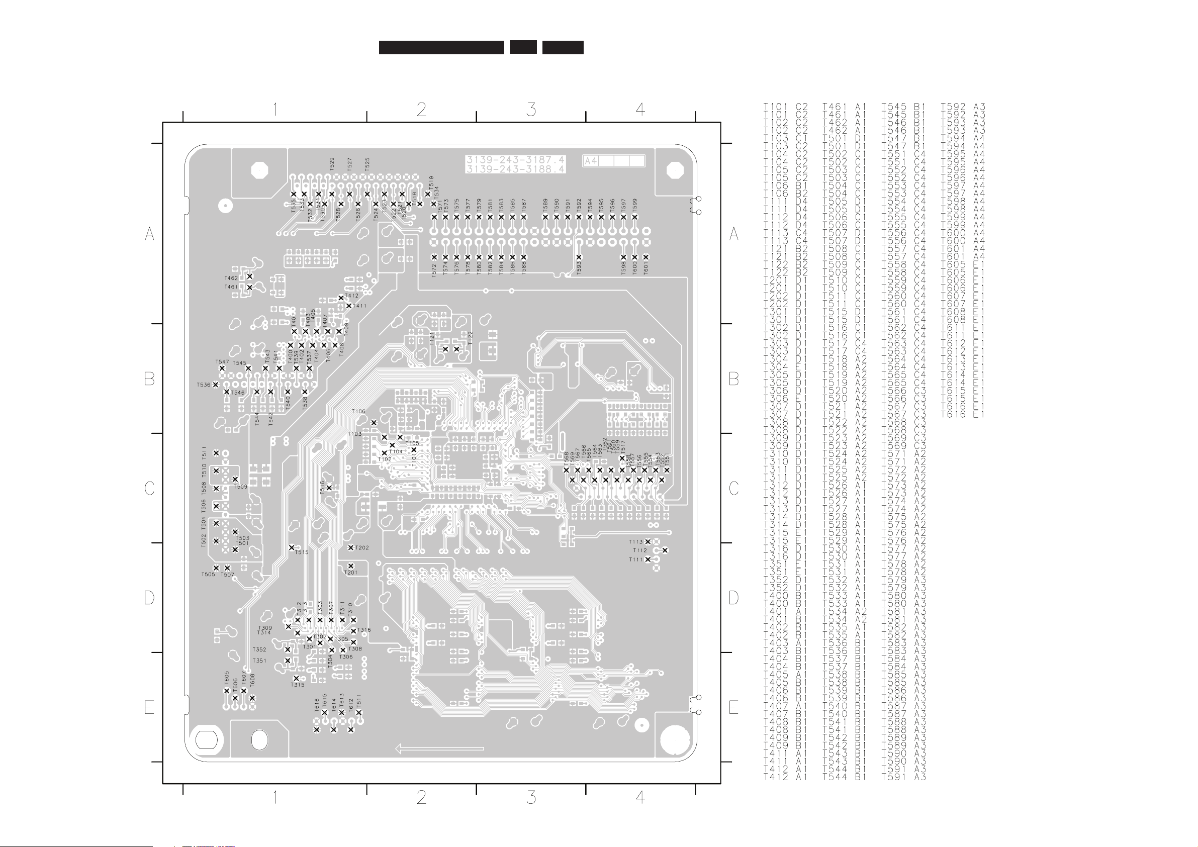
Test Points Overview for Digital Board
6.
Block Diagrams, Waveforms, Wiring Diagram.
3355 Testpoint-digital-31873.pdf 2005-04-01
 Loading...