

Philips DAC-08HN, DAC-08F, DAC-08EQF, DAC-08AF, DAC-08EN Datasheet
...
Philips Semiconductors Linear Products Product specification
DAC08 Series8-Bit high-speed multiplying D/A converter
716
August 31, 1994 853-0045 13721
DESCRIPTION
The DAC08 series of 8-bit monolithic multiplying Digital-to-Analog
Converters provide very high-speed performance coupled with low
cost and outstanding applications flexibility.
Advanced circuit design achieves 70ns settling times with very low
glitch and at low power consumption. Monotonic multiplying
performance is attained over a wide 20-to-1 reference current range.
Matching to within 1 LSB between reference and full-scale currents
eliminates the need for full-scale trimming in most applications.
Direct interface to all popular logic families with full noise immunity is
provided by the high swing, adjustable threshold logic inputs.
Dual complementary outputs are provided, increasing versatility and
enabling differential operation to effectively double the peak-to-peak
output swing. True high voltage compliance outputs allow direct
output voltage conversion and eliminate output op amps in many
applications.
All DAC08 series models guarantee full 8-bit monotonicity and
linearities as tight as 0.1% over the entire operating temperature
range. Device performance is essentially unchanged over the ±4.5V
to ±18V power supply range, with 37mW power consumption
attainable at ±5V supplies.
The compact size and low power consumption make the DAC08
attractive for portable and military aerospace applications.
FEATURES
•Fast settling output current—70ns
•Full-scale current prematched to ±1 LSB
•Direct interface to TTL, CMOS, ECL, HTL, PMOS
•Relative accuracy to 0.1% maximum over temperature range
•High output compliance -10V to +18V
•True and complemented outputs
•Wide range multiplying capability
•Low FS current drift — ±10ppm/°C
•Wide power supply range—±4.5V to ±18V
•Low power consumption—37mW at ±5V
APPLICATIONS
•8-bit, 1µs A-to-D converters
•Servo-motor and pen drivers
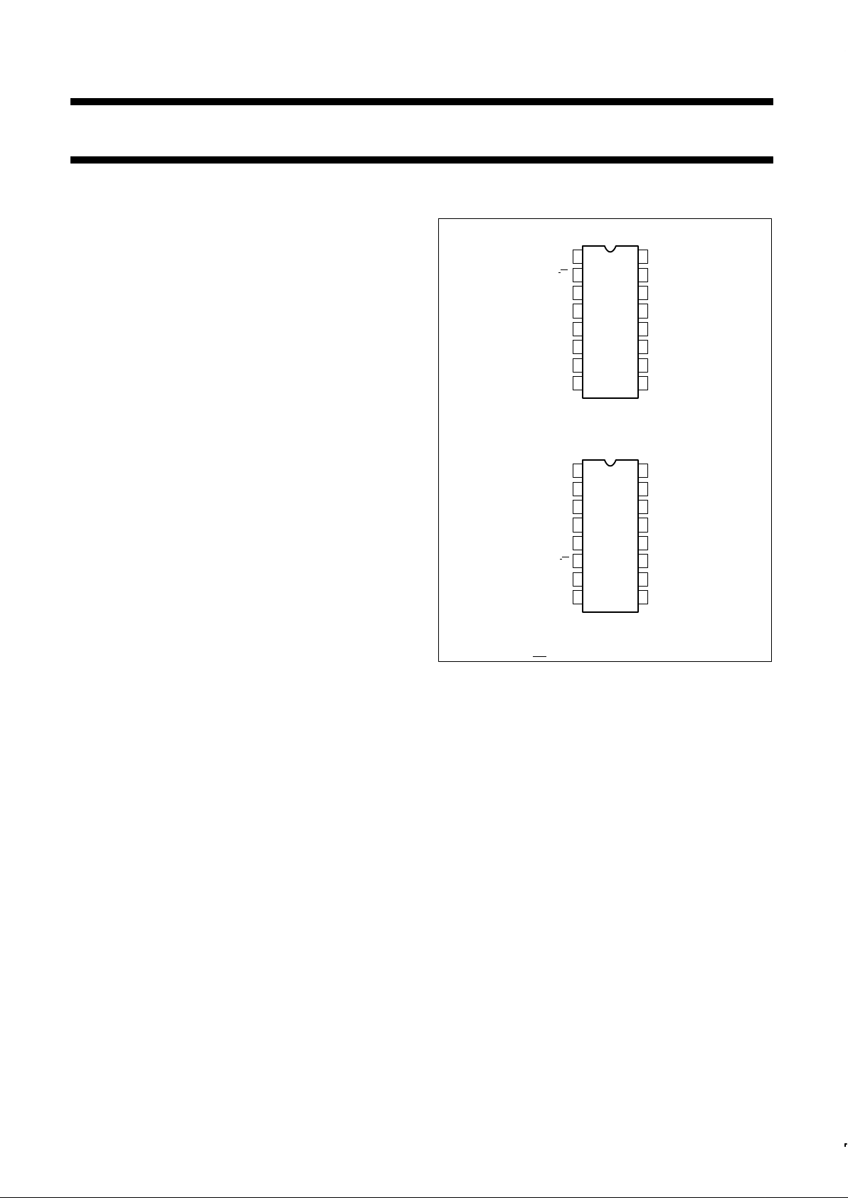
PIN CONFIGURATIONS
1
2
3
4
5
6
7
8
9
10
11
12
13
14
16
15
F, N Packages
D
1
Package
1
2
3
4
5
6
7
8
9
10
11
12
13
14
16
15
NOTE:
1. SO and
non-standard pinouts.
V
LC
I
O
V–
I
O
B1 (MSB)
B
2
B
3
B
4
COMP
V
REF–
V
REF+
V+
B
8
(LSB)
B
7
B
6
B
5
V+
V
REF+
V
REF–
COMPEN
V
LC
I
O
V–
I
O
B8 (LSB)
B
7
B
6
B
5
B
4
B
3
B
2
B1 (MSB)
TOP VIEW
TOP VIEW
•Waveform generators
•Audio encoders and attenuators
•Analog meter drivers
•Programmable power supplies
•CRT display drivers
•High-speed modems
•Other applications where low cost, high speed and complete in-
put/output versatility are required
•Programmable gain and attenuation
•Analog-Digital multiplication
Philips Semiconductors Linear Products Product specification
DAC08 Series8-Bit high-speed multiplying D/A converter
August 31, 1994
717
ORDERING INFORMATION
DESCRIPTION TEMPERATURE RANGE ORDER CODE DWG #
16-Pin Hermetic Ceramic Dual In-Line Package (Cerdip) -55°C to +125°C DAC08F 0582B
16-Pin Hermetic Ceramic Dual In-Line Package (Cerdip) -55°C to +125°C DAC08AF 0582B
16-Pin Plastic Dual In-Line Package (DIP) 0 to +70°C DAC08CN 0406C
16-Pin Hermetic Ceramic Dual In-Line Package (Cerdip) 0 to +70°C DAC08CF 0582B
16-Pin Plastic Dual In-Line Package (DIP) 0 to +70°C DAC08EN 0406C
16-Pin Hermetic Ceramic Dual In-Line Package (Cerdip) 0 to +70°C DAC08EF 0582B
16-Pin Plastic Small Outline (SO) Package 0 to +70°C DAC08ED 0005D
16-Pin Plastic Dual In-Line Package (DIP) 0 to +70°C DAC08HN 0406C
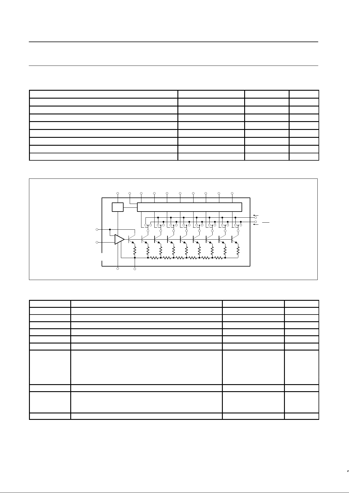
BLOCK DIAGRAM
BIAS
NETWORK
CURRENT
SWITCHES
MSB LSB
V+
13 1 5 6 7 8 9 10 11 12
14
15
16
3
4
2
COMP. V–
REFERENCE
AMPLIFIER
V
REF
(+)
V
REF
(–)
B
1
V
LC
B2B3B4B5B6B7B
8
I
OUT
+
–
I
OUT
ABSOLUTE MAXIMUM RATINGS
SYMBOL PARAMETER RATING UNIT
V+ to V- Power supply voltage 36 V
V5-V
12
Digital input voltage V- to V- plus 36V
V
LC
Logic threshold control V- to V+
V
0
Applied output voltage V- to +18 V
I
14
Reference current 5.0 mA
V14, V
15
Reference amplifier inputs VEE to V
CC
P
D
Maximum power dissipation TA=25°C
(still-air)
1
F package 1190 mW
N package 1450 mW
D package 1090 mW
T
SOLD
Lead soldering temperature (10sec max) 300 °C
T
A
Operating temperature range
DAC08, DAC08A -55 to +125 °C
DAC08C, E, H 0 to +70 °C
T
STG
Storage temperature range -65 to +150 °C
NOTES:
1. Derate above 25°C, at the following rates:
F package at 9.5mW/°C
N package at 11.6mW/°C
D package at 8.7mW/°C
Philips Semiconductors Linear Products Product specification
DAC08 Series8-Bit high-speed multiplying D/A converter
August 31, 1994
718
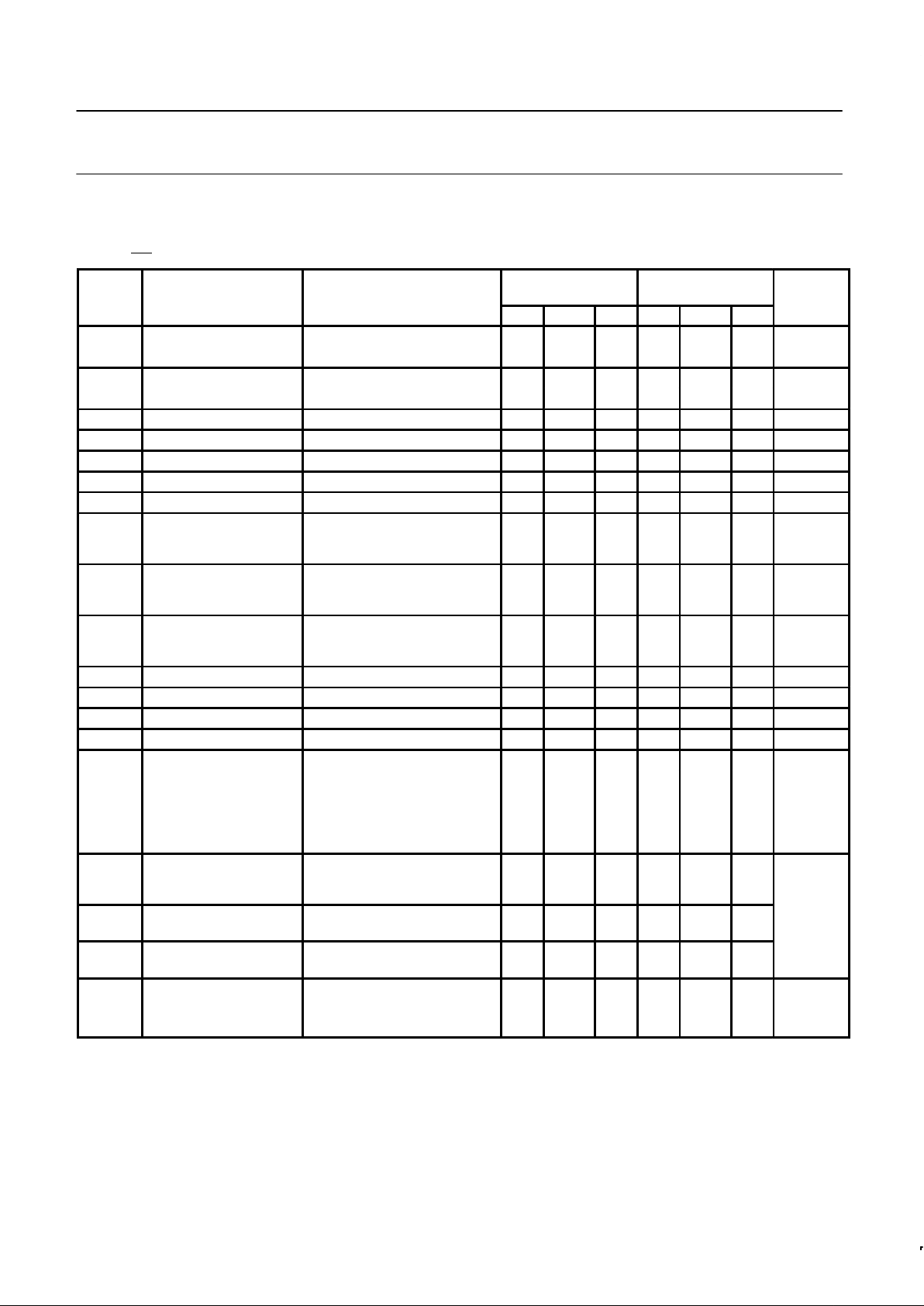
DC ELECTRICAL CHARACTERISTICS
Pin 3 must be at least 3V more negative than the potential to which R15 is returned. VCC=±15V, I
REF
=2.0mA. Output characteristics refer to both
I
OUT
and I
OUT
unless otherwise noted. DAC08C, E, H: TA=0°C to 70°C DAC08/08A: TA=-55°C to 125°C
SYMBOL
PARAMETER
TEST CONDITIONS
DAC08C
DAC08E
DAC08
UNIT
SYMBOL
PARAMETER
TEST CONDITIONS
Min Typ Max Min Typ Max
UNIT
Resolution 8 8 8 8 8 8 Bits
Monotonicity 8 8 8 8 8 8 Bits
Relative accuracy Over temperature range ±0.39 ±0.19 %FS
Differential non-linearity ±0.78 ±0.39 %FS
TCI
FS
Full-scale tempco ±10 ±10 ppm/°C
V
OC
Output voltage compliance Full-scale current change< 1/2LSB -10 +18 -10 +18 V
I
FS4
Full-scale current V
REF
=10.000V, R14, R15=5.000kΩ 1.94 1.99 2.04 1.94 1.99 2.04 mA
I
FSS
Full-scale symmetry I
FS4-IFS2
±2.0 ±16 ±1.0 ±8.0 µA
I
ZS
Zero-scale current 0.2 4.0 0.2 2.0 µA
I
FSR
Full-scale output current
range
R14, R15=5.000kΩ
V
REF
=+15.0V, V-=-10V
V
REF
=+25.0V, V-=-12V
2.1
4.2
2.1
4.2
mA
V
IL
V
IH
Logic input levels
Low
High
VLC=0V
2.0
0.8
2.0
0.8 V
I
IL
I
IH
Logic input current
Low
High
VLC=0V
V
IN
=-10V to +0.8V
V
IN
=2.0V to 18V
-2.0
0.002
-10
10
-2.0
0.002
-10
10
µA
V
IS
Logic input swing V-=-15V -10 +18 -10 +18 V
V
THR
Logic threshold range VS=±15V -10 +13.5 -10 +13.5 V
I
15
Reference bias current -1.0 -3.0 -1.0 -3.0 µA
dl/dt Reference input slew rate 4.0 8.0 4.0 8.0 mA/µs
Power supply sensitivity I
REF
=1mA
PSSI
FS+
Positive V+=4.5 to 5.5V, V-=-15V; 0.0003 0.01 0.0003 0.01
V+=13.5 to 16.5V, V-=-15V %FS/%VS
PSI
FS-
Negative V-=-4.5 to -5.5V, V+=+15V; 0.002 0.01 0.002 0.01
V-=-13.5 to -16.5, V+=+15V
I+
I-
Power supply current
Positive
Negative
VS=±5V, I
REF
=1.0mA
3.1
-4.3
3.8
-5.8
3.1
-4.3
3.8
-5.8
I+
I-
Positive
Negative
VS=+5V, -15V, I
REF
=2.0mA
3.1
-7.1
3.8
-7.8
3.1
-7.1
3.8
-7.8
mA
I+
I-
Positive
Negative
VS=±15V, I
REF
=2.0mA
3.2
-7.2
3.8
-7.8
3.2
-7.2
3.8
-7.8
±5V, I
REF
=1.0mA 37 48 37 48
P
D
Power dissipation
+5V, -15V, I
REF
=2.0mA 122 136 122 136 mW
D
±15V, I
REF
=2.0mA 156 174 156 174
Philips Semiconductors Linear Products Product specification
DAC08 Series8-Bit high-speed multiplying D/A converter
August 31, 1994
719
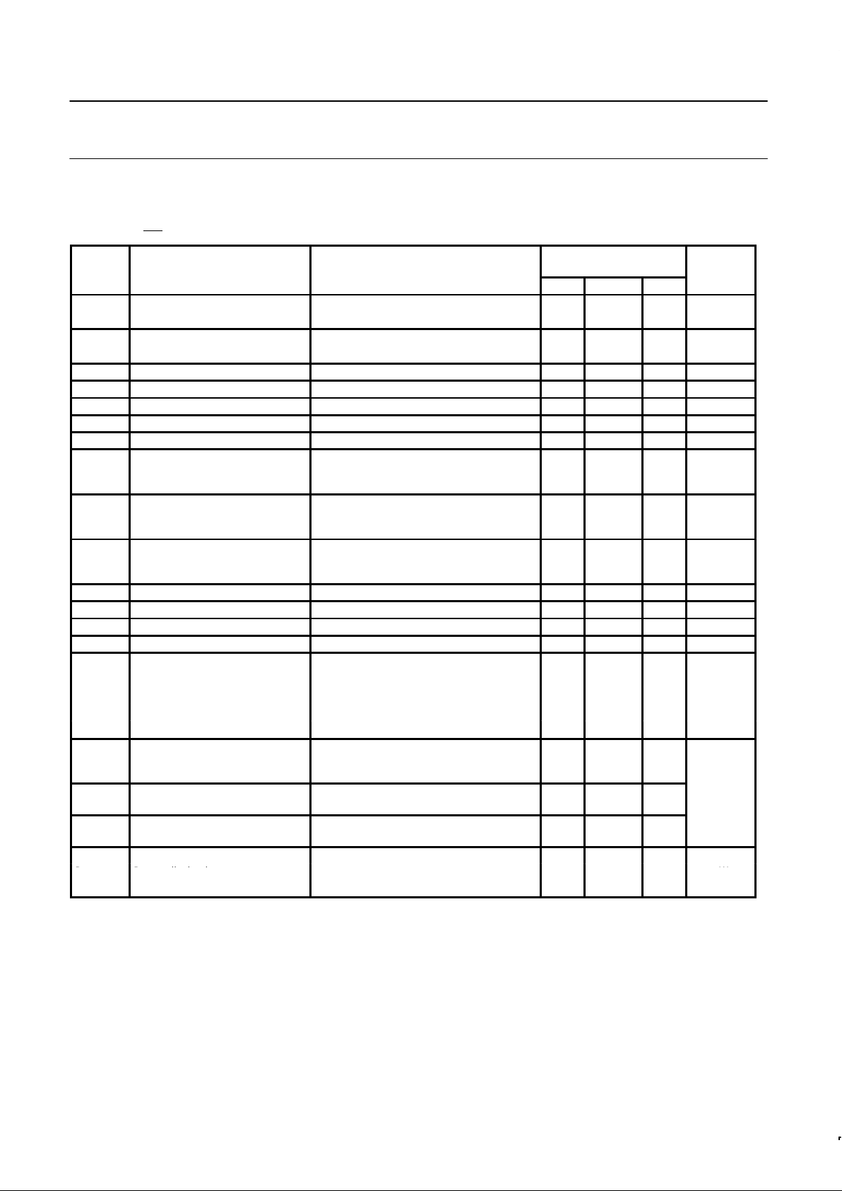
DC ELECTRICAL CHARACTERISTICS (Continued)
Pin 3 must be at least 3V more negative than the potential to which R15 is returned. V
CC
= +15V, I
REF
= 2.0mA, Output characteristics refer to
both I
OUT
and I
OUT
, unless otherwise noted. DAC08C, E, H: TA = 0°C to 70°C. DAC08/08A: TA = -55°C to 125°C.
SYMBOL
PARAMETER
TEST CONDITIONS
DAC08H
DAC08A
UNIT
SYMBOL
PARAMETER
TEST CONDITIONS
Min Typ Max
UNIT
Resolution 8 8 8 Bits
Monotonicity 8 8 8 Bits
Relative accuracy Over temperature range ±0.1 %FS
Differential non-linearity ±0.19 %FS
TCI
FS
Full-scale tempco ±10 ±50 ppm/°C
V
OC
Output voltage compliance Full-scale current change 1/2LSB -10 +18 V
I
FS4
Full-scale current V
REF
=10.000V, R14, R15=5.000kΩ 1.984 1.992 2.000 mA
I
FSS
Full-scale symmetry I
FS4-IFS2
±1.0 ±4.0 µA
I
ZS
Zero-scale current 0.2 1.0 µA
I
FSR
Full-scale output current range
R14, R15=5.000kΩ
V
REF
=+15.0V, V-=-10V
V
REF
=+25.0V, V-=-12V
2.1
4.2
mA
V
IL
V
IH
Logic input levels
Low
High
VLC=0V
2.0
0.8 V
I
IL
I
IH
Logic input current
Low
High
VLC=0V
V
IN
=-10V to +0.8V
V
IN
=2.0V to 18V
-2.0
0.002
-10
10
µA
V
IS
Logic input swing V-=-15V -10 +18 V
V
THR
Logic threshold range VS=±15V -10 +13.5 V
I
15
Reference bias current -1.0 -3.0 µA
dl/dt Reference input slew rate 4.0 8.0 mA/µs
Power supply sensitivity I
REF
=1mA
PSSI
FS+
Positive V+=4.5 to 5.5V, V-=-15V; 0.0003 0.01
V+=13.5 to 16.5V, V-=-15V %FS/%VS
PSI
FS-
Negative V-=-4.5 to -5.5V, V+=+15V; 0.002 0.01
V-=-13.5 to -16.5, V+=+15V
I+
I-
Power supply current
Positive
Negative
VS=±5V, I
REF
=1.0mA 3.1
-4.3
3.8
-5.8
I+
I-
Positive
Negative
VS=+5V, -15V, I
REF
=2.0mA
3.1
-7.1
3.8
-7.8
mA
I+
I-
Positive
Negative
VS=±15V, I
REF
=2.0mA
3.2
-7.2
3.8
-7.8
±5V, I
REF
=1.0mA 37 48
P
D
Power dissipation
+5V, -15V, I
REF
=2.0mA 122 136
mW
D
±15V, I
REF
=2.0mA 156 174
 Loading...