

Philips Semiconductors Linear Products Product specification
DAC08 Series8-Bit high-speed multiplying D/A converter
716
August 31, 1994 853-0045 13721
DESCRIPTION
The DAC08 series of 8-bit monolithic multiplying Digital-to-Analog
Converters provide very high-speed performance coupled with low
cost and outstanding applications flexibility.
Advanced circuit design achieves 70ns settling times with very low
glitch and at low power consumption. Monotonic multiplying
performance is attained over a wide 20-to-1 reference current range.
Matching to within 1 LSB between reference and full-scale currents
eliminates the need for full-scale trimming in most applications.
Direct interface to all popular logic families with full noise immunity is
provided by the high swing, adjustable threshold logic inputs.
Dual complementary outputs are provided, increasing versatility and
enabling differential operation to effectively double the peak-to-peak
output swing. True high voltage compliance outputs allow direct
output voltage conversion and eliminate output op amps in many
applications.
All DAC08 series models guarantee full 8-bit monotonicity and
linearities as tight as 0.1% over the entire operating temperature
range. Device performance is essentially unchanged over the ±4.5V
to ±18V power supply range, with 37mW power consumption
attainable at ±5V supplies.
The compact size and low power consumption make the DAC08
attractive for portable and military aerospace applications.
FEATURES
•Fast settling output current—70ns
•Full-scale current prematched to ±1 LSB
•Direct interface to TTL, CMOS, ECL, HTL, PMOS
•Relative accuracy to 0.1% maximum over temperature range
•High output compliance -10V to +18V
•True and complemented outputs
•Wide range multiplying capability
•Low FS current drift — ±10ppm/°C
•Wide power supply range—±4.5V to ±18V
•Low power consumption—37mW at ±5V
APPLICATIONS
•8-bit, 1µs A-to-D converters
•Servo-motor and pen drivers
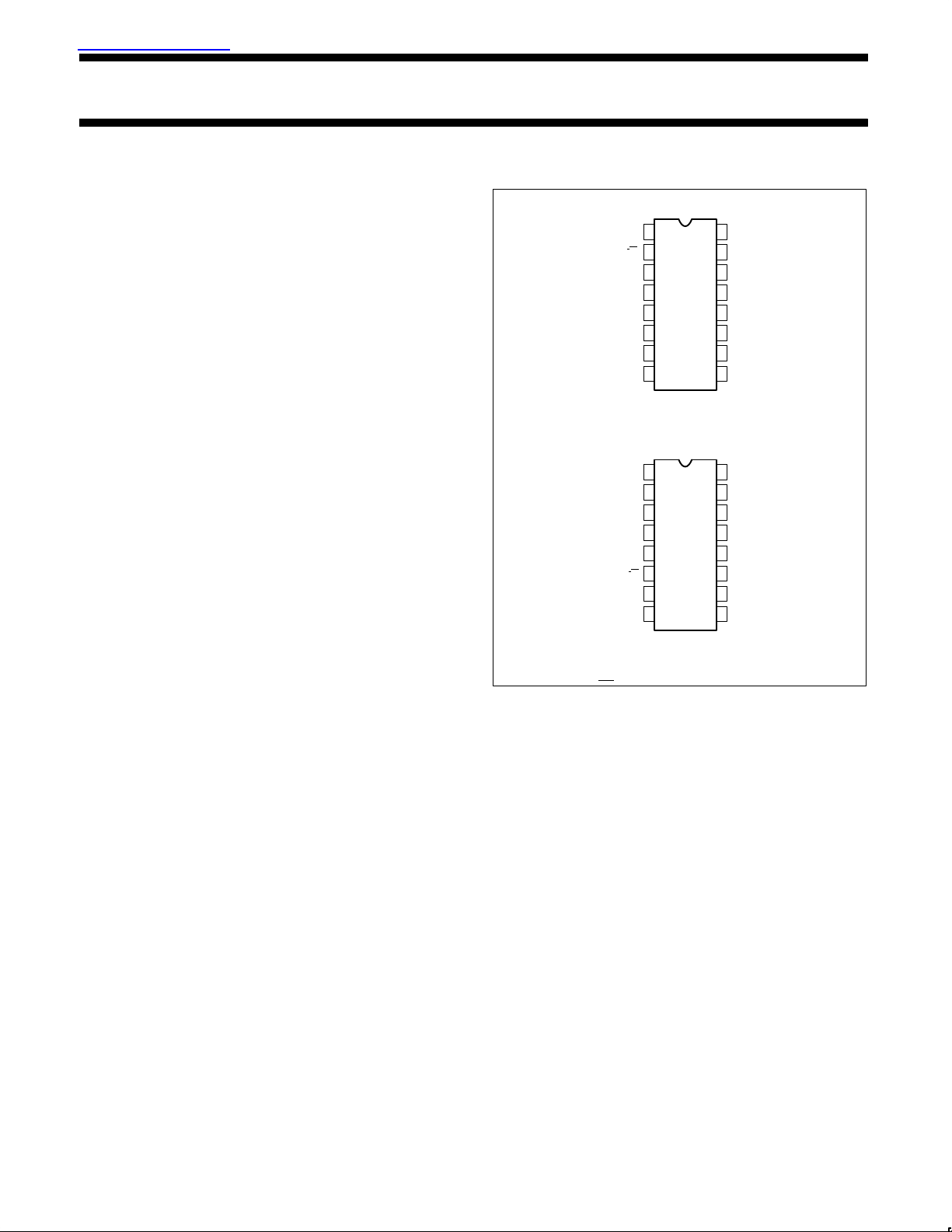
PIN CONFIGURATIONS
1
2
3
4
5
6
7
8
9
10
11
12
13
14
16
15
F, N Packages
D
1
Package
1
2
3
4
5
6
7
8
9
10
11
12
13
14
16
15
NOTE:
1. SO and
non-standard pinouts.
V
LC
I
O
V–
I
O
B1 (MSB)
B
2
B
3
B
4
COMP
V
REF–
V
REF+
V+
B
8
(LSB)
B
7
B
6
B
5
V+
V
REF+
V
REF–
COMPEN
V
LC
I
O
V–
I
O
B8 (LSB)
B
7
B
6
B
5
B
4
B
3
B
2
B1 (MSB)
TOP VIEW
TOP VIEW
•Waveform generators
•Audio encoders and attenuators
•Analog meter drivers
•Programmable power supplies
•CRT display drivers
•High-speed modems
•Other applications where low cost, high speed and complete in-
put/output versatility are required
•Programmable gain and attenuation
•Analog-Digital multiplication
查询NE5008供应商

Philips Semiconductors Linear Products Product specification
DAC08 Series8-Bit high-speed multiplying D/A converter
August 31, 1994
717
ORDERING INFORMATION
DESCRIPTION TEMPERATURE RANGE ORDER CODE DWG #
16-Pin Hermetic Ceramic Dual In-Line Package (Cerdip) -55°C to +125°C DAC08F 0582B
16-Pin Hermetic Ceramic Dual In-Line Package (Cerdip) -55°C to +125°C DAC08AF 0582B
16-Pin Plastic Dual In-Line Package (DIP) 0 to +70°C DAC08CN 0406C
16-Pin Hermetic Ceramic Dual In-Line Package (Cerdip) 0 to +70°C DAC08CF 0582B
16-Pin Plastic Dual In-Line Package (DIP) 0 to +70°C DAC08EN 0406C
16-Pin Hermetic Ceramic Dual In-Line Package (Cerdip) 0 to +70°C DAC08EF 0582B
16-Pin Plastic Small Outline (SO) Package 0 to +70°C DAC08ED 0005D
16-Pin Plastic Dual In-Line Package (DIP) 0 to +70°C DAC08HN 0406C
BLOCK DIAGRAM
BIAS
NETWORK
CURRENT
SWITCHES
MSB LSB
V+
13 1 5 6 7 8 9 10 11 12
14
15
16
3
4
2
COMP. V–
REFERENCE
AMPLIFIER
V
REF
(+)
V
REF
(–)
B
1
V
LC
B2B3B4B5B6B7B
8
I
OUT
+
–
I
OUT
ABSOLUTE MAXIMUM RATINGS
SYMBOL PARAMETER RATING UNIT
V+ to V- Power supply voltage 36 V
V5-V
12
Digital input voltage V- to V- plus 36V
V
LC
Logic threshold control V- to V+
V
0
Applied output voltage V- to +18 V
I
14
Reference current 5.0 mA
V14, V
15
Reference amplifier inputs VEE to V
CC
P
D
Maximum power dissipation TA=25°C
(still-air)
1
F package 1190 mW
N package 1450 mW
D package 1090 mW
T
SOLD
Lead soldering temperature (10sec max) 300 °C
T
A
Operating temperature range
DAC08, DAC08A -55 to +125 °C
DAC08C, E, H 0 to +70 °C
T
STG
Storage temperature range -65 to +150 °C
NOTES:
1. Derate above 25°C, at the following rates:
F package at 9.5mW/°C
N package at 11.6mW/°C
D package at 8.7mW/°C
Philips Semiconductors Linear Products Product specification
DAC08 Series8-Bit high-speed multiplying D/A converter
August 31, 1994
718
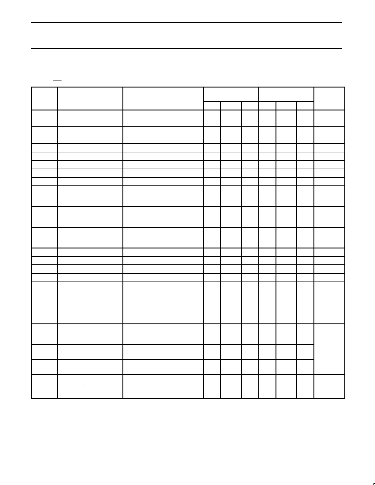
DC ELECTRICAL CHARACTERISTICS
Pin 3 must be at least 3V more negative than the potential to which R15 is returned. VCC=±15V, I
REF
=2.0mA. Output characteristics refer to both
I
OUT
and I
OUT
unless otherwise noted. DAC08C, E, H: TA=0°C to 70°C DAC08/08A: TA=-55°C to 125°C
SYMBOL
PARAMETER
TEST CONDITIONS
DAC08C
DAC08E
DAC08
UNIT
SYMBOL
PARAMETER
TEST CONDITIONS
Min Typ Max Min Typ Max
UNIT
Resolution 8 8 8 8 8 8 Bits
Monotonicity 8 8 8 8 8 8 Bits
Relative accuracy Over temperature range ±0.39 ±0.19 %FS
Differential non-linearity ±0.78 ±0.39 %FS
TCI
FS
Full-scale tempco ±10 ±10 ppm/°C
V
OC
Output voltage compliance Full-scale current change< 1/2LSB -10 +18 -10 +18 V
I
FS4
Full-scale current V
REF
=10.000V, R14, R15=5.000kΩ 1.94 1.99 2.04 1.94 1.99 2.04 mA
I
FSS
Full-scale symmetry I
FS4-IFS2
±2.0 ±16 ±1.0 ±8.0 µA
I
ZS
Zero-scale current 0.2 4.0 0.2 2.0 µA
I
FSR
Full-scale output current
range
R14, R15=5.000kΩ
V
REF
=+15.0V, V-=-10V
V
REF
=+25.0V, V-=-12V
2.1
4.2
2.1
4.2
mA
V
IL
V
IH
Logic input levels
Low
High
VLC=0V
2.0
0.8
2.0
0.8 V
I
IL
I
IH
Logic input current
Low
High
VLC=0V
V
IN
=-10V to +0.8V
V
IN
=2.0V to 18V
-2.0
0.002
-10
10
-2.0
0.002
-10
10
µA
V
IS
Logic input swing V-=-15V -10 +18 -10 +18 V
V
THR
Logic threshold range VS=±15V -10 +13.5 -10 +13.5 V
I
15
Reference bias current -1.0 -3.0 -1.0 -3.0 µA
dl/dt Reference input slew rate 4.0 8.0 4.0 8.0 mA/µs
Power supply sensitivity I
REF
=1mA
PSSI
FS+
Positive V+=4.5 to 5.5V, V-=-15V; 0.0003 0.01 0.0003 0.01
V+=13.5 to 16.5V, V-=-15V %FS/%VS
PSI
FS-
Negative V-=-4.5 to -5.5V, V+=+15V; 0.002 0.01 0.002 0.01
V-=-13.5 to -16.5, V+=+15V
I+
I-
Power supply current
Positive
Negative
VS=±5V, I
REF
=1.0mA
3.1
-4.3
3.8
-5.8
3.1
-4.3
3.8
-5.8
I+
I-
Positive
Negative
VS=+5V, -15V, I
REF
=2.0mA
3.1
-7.1
3.8
-7.8
3.1
-7.1
3.8
-7.8
mA
I+
I-
Positive
Negative
VS=±15V, I
REF
=2.0mA
3.2
-7.2
3.8
-7.8
3.2
-7.2
3.8
-7.8
±5V, I
REF
=1.0mA 37 48 37 48
+5V, -15V, I
REF
=2.0mA 122 136 122 136 mW
D
±15V, I
REF
=2.0mA 156 174 156 174
P
D
Power dissipation

Philips Semiconductors Linear Products Product specification
DAC08 Series8-Bit high-speed multiplying D/A converter
August 31, 1994
719
DC ELECTRICAL CHARACTERISTICS (Continued)
Pin 3 must be at least 3V more negative than the potential to which R15 is returned. V
CC
= +15V, I
REF
= 2.0mA, Output characteristics refer to
both I
OUT
and I
OUT
, unless otherwise noted. DAC08C, E, H: TA = 0°C to 70°C. DAC08/08A: TA = -55°C to 125°C.
SYMBOL
PARAMETER
TEST CONDITIONS
DAC08H
DAC08A
UNIT
SYMBOL
PARAMETER
TEST CONDITIONS
Min Typ Max
UNIT
Resolution 8 8 8 Bits
Monotonicity 8 8 8 Bits
Relative accuracy Over temperature range ±0.1 %FS
Differential non-linearity ±0.19 %FS
TCI
FS
Full-scale tempco ±10 ±50 ppm/°C
V
OC
Output voltage compliance Full-scale current change 1/2LSB -10 +18 V
I
FS4
Full-scale current V
REF
=10.000V, R14, R15=5.000kΩ 1.984 1.992 2.000 mA
I
FSS
Full-scale symmetry I
FS4-IFS2
±1.0 ±4.0 µA
I
ZS
Zero-scale current 0.2 1.0 µA
I
FSR
Full-scale output current range
R14, R15=5.000kΩ
V
REF
=+15.0V, V-=-10V
V
REF
=+25.0V, V-=-12V
2.1
4.2
mA
V
IL
V
IH
Logic input levels
Low
High
VLC=0V
2.0
0.8 V
I
IL
I
IH
Logic input current
Low
High
VLC=0V
V
IN
=-10V to +0.8V
V
IN
=2.0V to 18V
-2.0
0.002
-10
10
µA
V
IS
Logic input swing V-=-15V -10 +18 V
V
THR
Logic threshold range VS=±15V -10 +13.5 V
I
15
Reference bias current -1.0 -3.0 µA
dl/dt Reference input slew rate 4.0 8.0 mA/µs
Power supply sensitivity I
REF
=1mA
PSSI
FS+
Positive V+=4.5 to 5.5V, V-=-15V; 0.0003 0.01
V+=13.5 to 16.5V, V-=-15V %FS/%VS
PSI
FS-
Negative V-=-4.5 to -5.5V, V+=+15V; 0.002 0.01
V-=-13.5 to -16.5, V+=+15V
I+
I-
Power supply current
Positive
Negative
VS=±5V, I
REF
=1.0mA 3.1
-4.3
3.8
-5.8
I+
I-
Positive
Negative
VS=+5V, -15V, I
REF
=2.0mA
3.1
-7.1
3.8
-7.8
mA
I+
I-
Positive
Negative
VS=±15V, I
REF
=2.0mA
3.2
-7.2
3.8
-7.8
±5V, I
REF
=1.0mA 37 48
+5V, -15V, I
REF
=2.0mA 122 136
D
±15V, I
REF
=2.0mA 156 174
P
D
Power dissipation
mW

Philips Semiconductors Linear Products Product specification
DAC08 Series8-Bit high-speed multiplying D/A converter
August 31, 1994
720
AC ELECTRICAL CHARACTERISTICS
SYMBOL
PARAMETER
TEST CONDITIONS
DAC08C
DAC08E
DAC08
DAC08H
DAC08A
UNIT
SYMBOL
PARAMETER
TEST CONDITIONS
Min Typ Max Min Typ Max Min Typ Max
UNIT
t
S
Settling time
To ± 1/2LSB, all bits
switched on or off,
T
A
=25°C
70 135 70 135 70 135 ns
Propagation delay
t
PLH
Low-to-High TA=25°C, each bit. ns
t
PHL
High-to-Low All bits switched 35 60 35 60 35 60
TEST CIRCUITS
Figure 1. Relative Accuracy Test Circuit
CONTROL
LOGIC
DAC-08
REFERENCE DAC
ACCURACY > 0.006%
NE5534
ERROR
OUTPUT
V– V+
–
+
16
14
15 5-12 1 2
4
133
V
REF
R
REF
R
f
R15
Figure 2. Transient Response and Settling Time
FOR SETTLING TIME
MEASUREMENT
(ALL BITS
SWITCHED LOW
TO HIGH)
USE R
L
to GND
FOR TURN OFF
MEASUREMENT
SETTLING TIME
TRANSIENT
RESPONSE
e
IN
2.4V
0.4V
1.0V
0
0
-100mV
1.4V
R
L
= 500Ω
R
L
= 50Ω
PIN 4 TO GND
t
S
= 70ns TYPICAL
TO ±1/2 LSB
t
PHL
= t
PLH
= 10ns
t
PHL
t
PLH
CO ≤ 25pF
15pF
51
5
6
7
8
9
10
11
12
3
13
14
15
1
2
4
16
DAC-08
V
EE
V
CC
e
IN
e
O
0.1µF
0.1µF
1.0k
1.0k
0.1µF
R
L
+2.0V
DC

Philips Semiconductors Linear Products Product specification
DAC08 Series8-Bit high-speed multiplying D/A converter
August 31, 1994
721
TEST CIRCUITS (Continued)
Figure 3. Reference Current Slew Rate Measurement
5
6
7
8
9
10
11
12
3
13
14
15
1
2
4
16
DAC-08
V
EE
V
CC
0.1µF
OPEN
SCOPE
REQ = 200Ω
R
L
R
P
1k
R
IN
V
IN
dI
dt
I
R
L
dV
dt
SLEWING TIME
10%
90%
0
2.0mA
2V
0
Figure 4. Notation Definitions
NOTES:
(See text for values of C.)
Typical values of R
14
= R15 = 1k
V
REF
= +2.0V
C = 15pF
VI and II apply to inputs A1 through A
8
The resistor tied to Pin 15 is to temperature compensate the bias current and may not be necessary for all applications.
I
O
K
A
1
2
A
2
4
A
3
8
A
4
16
A
5
32
A
6
64
A
7
128
A
8
256
where K
V
REF
R
14
and AN = ‘1’ if AN is at High Level
A
N
= ‘0’ if AN is at Low Level
5
6
7
8
9
10
11
12
3
13
14
15
1
2
4
16
DAC-08
V
CC
DIGITAL
INPUTS
OUTPUT
I
CC
V
O
V
REF
(+)
I
O
R
L
C
V
EE
I
EE
V
I
I
I
(+)
R
15
R
14
I
15
I
14
A
1
A
2
A
3
A
4
A
5
A
6
A
7
A
8

Philips Semiconductors Linear Products Product specification
DAC08 Series8-Bit high-speed multiplying D/A converter
August 31, 1994
722
TYPICAL PERFORMANCE CHARACTERISTICS
10
I
FS
— OUTPUT FULL SCALE CURRENT (mA)
50ns/DIVISIOM
R
EQ
= 200Ω, RL = 100Ω, CC = 0
2.0mA
NOTES:
Curve 1: CC = 15pF, V
IN
= 2.0V
P-P
centered at +1.0V
Curve 1: CC = 15pF, V
IN
= 5m0V
P-P
centered at +200mV
Curve 1: CC = 15pF, V
IN
= 100m0V
P-P
centered at 0V
and applied through 50Ω connected to Pin 14.
+2.0V applied to R
14
.
Output Current vs Output Voltage
(Output Voltage Compliance)
Fast Pulsed Reference Operation
True and Complementary Output
Operation
Full-Scale Settling Time LSB Switching
Full-Scale Current vs
Reference Current
LSB Propagation Delay vs IFS
Reference Input Frequency Response
I
REF
— REFERENCE CURRENT (mA)
5.0
4.0
3.0
2.0
1.0
0
0 1.0 2.0 3.0 4.0 5.0
I – OUTPUT CURRENT (mA)
FS
TA = T
min
TO T
max
ALL BITS “HIGH”
LIMIT FOR
V–=–15V
LIMIT FOR
V–=–5V
(00000000) (11111111)
0mA
1.0mA
I
OUT
I
OUT
3.2
2.8
2.4
2.0
1.6
1.2
0.8
0.4
0
OUTPUT CURRENT (mA)
OUTPUT VOLTAGE (V)
ALL BITS ON
–14 –10 –6 –2 0 2 6 10 14 18
2.5V
0.5V
–0.5mA
–2.5mA
V
IN
I
OUT
200ns/division
BIT 8
LOGIC
INPUT
I
OUT
8µA
2.4V
0.4V
0V
0
ALL BITS SWITCHED ON
OUTPUT – 1/2LSB
SETTLING +1/2LSB
0
2.4V
0.4V
50ns/DIVISIOM
I
FS
=2mA, RL=1kΩ 1/2LSB=4µA
500
400
300
200
100
0
.05
.01
.02
.05
0.1
0.2
0.5
1.0
2.0
5.0
10
PROPAGATION DELAY (ns)
1LSB=78nA
1LSB=7.8µA
RELATIVE OUTPUT (dB)
FREQUENCY (MHz)
6
4
2
0
–2
–4
–6
–8
–10
–12
–14
0.1 0.2 0.5 1.0 2.0 5.0
R14=R15=1kΩ
3
2
1
RL ≤ 500Ω
ALL BITS “ON”
VR15 = 0V
I
REF
= 0.2mA
I
REF
= 1mA
I
REF
= 2mA
V– = –15V V– = –5V
TA = T
min
TO T
max

Philips Semiconductors Linear Products Product specification
DAC08 Series8-Bit high-speed multiplying D/A converter
August 31, 1994
723
TYPICAL PERFORMANCE CHARACTERISTICS (Continued)
OUTPUT CURRENT (mA)
LOGIC INPUT VOLTAGE (V)
LOGIC INPUT CURRENT ( A)
µ
10,000
POWER SUPPLY CURRENT (mA)
POWER SUPPLY CURRENT (mA)
NOTES:
B1 through B8 have identical transfer characteristics.
Bits are fully switched, with less than 1/2LSB error, at
less than ±100mV from actual threshold. These
switching points are guaranteed to lie between 0.8 and
2.0V over the operating temperature range
(V
LC
= 0.0V).
Reference AMP Common-Mode Range
All Bits On
Logic Input Current vs Input Voltage
V
TH
– VLC vs Temperature
Output Voltage Compliance
vs Temperature
Bit Transfer Characteristics
Power Supply Current vs V+
Power Supply Current vs V– Power Supply Current vs Temperature
Maximum Reference Input Frequency
vs Compensation Capacitor Value
2.0
1.8
1.6
1.4
1.2
1.o
0.8
0.6
0.4
0.2
0
–50 0 50 100 150
V – V (V)
THLC
TEMPERATURE (°C)
8
7
6
5
4
3
2
1
0
0 –4.0 –8.0 –12 –16 –20
V– — NEGATIVE POWER SUPPLY (V
DC
)
I+
BITS MAY BE HIGH OR LOW
I– WITH I
REF
= 2mA
I– WITH I
REF
= 1mA
I– WITH I
REF
= 0.2mA
8
7
6
5
4
3
2
1
0
–50 0 50 100 150
TEMPERATURE (°C)
BITS MAY BE HIGH OR LOW
I
REF
= 2.0mA
I+
I–
V+ = +15V
V– = +15V
1,000
100
10
1
10
100
1000
CC (pF)
F (kHz)
MAX
8.0
6.0
4.0
2.0
0
–12 –8 –4 0 4 8 12 16
LOGIC INPUT VOLTAGE (V)
1.4
20
3.2
2.8
2.4
2.0
1.6
1.2
0.8
0.4
0
–14 –10 –6 –2 0 2 6 10 14 18
V15 — REFERENCE COMMON MODE VOLTAGE (V)
POSITIVE COMMON-MODE RANGE IS ALWAYS (V+) –1.5V.
I
REF
= 2mA
TA = T
MIN
to T
MAX
I
REF
= 1mA
I
REF
= 0.2mA
V– = –15V V– = –5V V+ = +5V
POWER SUPPLY CURRENT (mA)
8
7
6
5
4
3
2
1
0
–50 0 50 100 150
V+ – POSITIVE POWER SUPPLY (V
DC
)
ALL BITS HIGH OR LOW
I+
I–
1.2
1.0
0.8
0.6
0.4
0.2
0
–12 –8 –4 0 4 8 12 16
OUTPUT CURRENT (mA)
I
REF
= 2.0mA
B
1
B
2
B
3
B
4
B
5
V– = –15V
V– = –5V
Shaded area indicates
permissible output voltage
range for V– = -15V, I
REF
≤ 2.0mA
For other V– or I
REF
See “Output Current vs Output
Voltage” curve on previous page
TEMPERATURE (°C)
16
12
8
4
0
–4
–8
–12
–50 0 50 100 150
OUTPUT VOLTAGE (V)

Philips Semiconductors Linear Products Product specification
DAC08 Series8-Bit high-speed multiplying D/A converter
August 31, 1994
724
TYPICAL APPLICATION
NOTES:
REQ = R
IN
|| R
P
Typical Values
R
IN
= 5kΩ
+V
IN
= 10V
Pulsed Referenced Operation
OPTIONAL RESISTOR
FOR OFFSET
INPUTS
NO CAP
14
15
16
2
4
+V
REF
R
REF
REQ
=200Ω
R
P
R
IN
0V
FUNCTIONAL DESCRIPTION
Reference Amplifier Drive and Compensation
The reference amplifier input current must always flow into Pin 14
regardless of the setup method or reference supply voltage polarity.
Connections for a positive reference voltage are shown in Figure 1.
The reference voltage source supplies the full reference current. For
bipolar reference signals, as in the multiplying mode, R
15
can be
tied to a negative voltage corresponding to the minimum input level.
R
15
may be eliminated with only a small sacrifice in accuracy and
temperature drift.
The compensation capacitor value must be increased as R
14
value
is increased. This is in order to maintain proper phase margin. For
R
14
values of 1.0, 2.5, and 5.0kΩ, minimum capacitor values are 15,
37, and 75pF, respectively. The capacitor may be tied to either V
EE
or ground, but using VEE increases negative supply rejection.
(Fluctuations in the negative supply have more effect on accuracy
than do any changes in the positive supply.)
A negative reference voltage may be used if R
14
is grounded and
the reference voltage is applied to R
15
as shown. A high input
impedance is the main advantage of this method. The negative
reference voltage must be at least 3.0V above the V
EE
supply.
Bipolar input signals may be handled by connecting R
14
to a positive
reference voltage equal to the peak positive input level at Pin 15.
When using a DC reference voltage, capacitive bypass to ground is
recommended. The 5.0V logic supply is not recommended as a
reference voltage, but if a well regulated 5.0V supply which drives
logic is to be used as the reference, R
14
should be formed of two
series resistors with the junction of the two resistors bypassed with
0.1µF to ground. For reference voltages greater than 5.0V, a clamp
diode is recommended between Pin 14 and ground.
If Pin 14 is driven by a high impedance such as a transistor current
source, none of the above compensation methods applies and the
amplifier must be heavily compensated, decreasing the overall
bandwidth.
Output Voltage Range
The voltage at Pin 4 must always be at least 4.5V more positive than
the voltage of the negative supply (Pin 3) when the reference current
is 2mA or less, and at least 8V more positive than the negative
supply when the reference current is between 2mA and 4mA. This is
necessary to avoid saturation of the output transistors, which would
cause serious accuracy degradation.
Output Current Range
Any time the full-scale current exceeds 2mA, the negative supply
must be at least 8V more negative than the output voltage. This is
due to the increased internal voltage drops between the negative
supply and the outputs with higher reference currents.
Accuracy
Absolute accuracy is the measure of each output current level with
respect to its intended value, and is dependent upon relative
accuracy, full-scale accuracy and full-scale current drift. Relative
accuracy is the measure of each output current level as a fraction of
the full-scale current after zero-scale current has been nulled out.
The relative accuracy of the DAC08 series is essentially constant
over the operating temperature range due to the excellent
temperature tracking of the monolithic resistor ladder. The reference
current may drift with temperature, causing a change in the absolute
accuracy of output current. However, the DAC08 series has a very
low full-scale current drift over the operating temperature range.
The DAC08 series is guaranteed accurate to within ± LSB at +25°C
at a full-scale output current of 1.992mA. The relative accuracy test
circuit is shown in Figure 1. The 12-bit converter is calibrated to a
full-scale output current of 1.99219mA, then the DAC08 full-scale
current is trimmed to the same value with R
14
so that a zero value
appears at the error amplifier output. The counter is activated and
the error band may be displayed on the oscilloscope, detected by
comparators, or stored in a peak detector.
Two 8-bit D-to-A converters may not be used to construct a 16-bit
accurate D-to-A converter. 16-bit accuracy implies a total of ± part in
65,536, or ±0.00076%, which is much more accurate than the
±0.19% specification of the DAC08 series.
Monotonicity
A monotonic converter is one which always provides analog output
greater than or equal to the preceding value for a corresponding
increment in the digital input code. The DAC08 series is monotonic
for all values of reference current above 0.5mA. The recommended
range for operation is a DC reference current between 0.5mA and
4.0mA.
Settling Time
The worst-case switching condition occurs when all bits are
switched on, which corresponds to a low-to-high transition for all
input bits. This time is typically 70ns for settling to within LSB for
8-bit accuracy. This time applies when R
L
<500Ω and CO<25pF. The
slowest single switch is the least significant bit, which typically turns
on and settles in 65ns. In applications where the DAC functions in a
positive-going ramp mode, the worst-case condition does not occur
and settling times less than 70ns may be realized.
Extra care must be taken in board layout since this usually is the
dominant factor in satisfactory test results when measuring settling
time. Short leads, 100µF supply bypassing for low frequencies,
minimum scope lead length, and avoidance of ground loops are all
mandatory.

Philips Semiconductors Linear Products Product specification
DAC08 Series8-Bit high-speed multiplying D/A converter
August 31, 1994
725
SETTLING TIME AND PROPAGATION DELAY
NOTES:
D
1
, D2 = IN6263 or equivalent
D
3
= IN914 or equivalent
C
1
= 0.01µF
C
2
, C3 = 0.1µF
Q
1
= 2N3904
C
4
, C5 = 15pF and includes all probe and fixturing capacitance.
V
IN
VS + = +15V
V
ADJ
V
OUT
VS – = –15V
R
15
= 5kΩ
I
REF
= 2mA
V
REF
= 10V
R
14
= 5kΩ
V
OUT
R1 = 1000Ω
R
2
= 1000Ω
R
3
= 500Ω
50Ω
C
1
C
2
C
5
C
3
D
3
D
1
D
2
C
4
DUT
14
15
16 3 1
2
4
12111098765
Q
1
BASIC DAC08 CONFIGURATION
NOTES:
I
FS
V
REF
R
REF
x
255
256
; IO IO IFSfor all logic states
MSB 2 3 4 5 6 7 LSB
5 6 7 8 9 10 11 12
14
15
3 16
13
1
2
4
DAC-08
(LOW T.C.)
V+
V–
I
O
I
O
+V
REF
I
REF
R
REF
C
COMP
0.1µF
0.1µF

Philips Semiconductors Linear Products Product specification
DAC08 Series8-Bit high-speed multiplying D/A converter
August 31, 1994
726
RECOMMENDED FULL-SCALE AND ZERO-SCALE ADJUST
NOTES:
R
1
= low T.C.
R
3
= R1 + R
2
R2 ≈ 0.1 R1 to minimize pot. contribution to full-scale drift
14
15
2
4
DAC-08
V
REF
V+
V–
R
4
= 1MΩ
R
S
= 20kΩ
R
3
R
2
R
1
UNIPOLAR VOLTAGE OUTPUT FOR LOW IMPEDANCE OUTPUT
V
OUT
=
14
15
DAC-08
–
+
NE531
OR
EQUIV 0 TO +10V
I
R
= 2mA
4
2
5kΩ
5kΩ (LOW T.C.)

Philips Semiconductors Linear Products Product specification
DAC08 Series8-Bit high-speed multiplying D/A converter
August 31, 1994
727
UNIPOLAR VOLTAGE OUTPUT FOR HIGH IMPEDANCE OUTPUT
14
2
4
DAC-08
IR = 2mA
V
OUT
V
OUT
5kΩ 5kΩ
V = 10V
14
2
4
DAC-08
IR = 2mA
V
OUT
V
OUT
a. Positive Output
a. Negative Output
BASIC BIPOLAR OUTPUT OPERATION (OFFSET BINARY)
1
1
1
1
0
0
0
1
1
0
0
1
0
0
1
1
0
0
1
0
0
1
1
0
0
1
0
0
1
1
0
0
1
0
0
1
1
0
0
1
0
0
1
1
0
0
1
0
0
1
0
1
0
1
1
0
Positive full-scale
Positive FS – 1LSB
+ Zero-scale + 1LSB
Zero-scale
Zero-scale – 1LSB
Negative full scale – 1LSB
Negative full scale
–9.920V
–9.840V
–0.080V
0.000
0.080
+9.920
+10.000
+10.000
+9.920
+0.160
+0.080
0.000
–9.840
–9.920
B
1B2B3B4B5B6B7B8
V
OUT
V
OUT
14
2
4
DAC-08
IR = 2mA
V
OUT
V
OUT
10kΩ
V = 10V
10kΩ

Copyright © Each Manufacturing Company.
All Datasheets cannot be modified without permission.
This datasheet has been download from :
www.AllDataSheet.com
100% Free DataSheet Search Site.
Free Download.
No Register.
Fast Search System.
www.AllDataSheet.com
 Loading...